EP2450309A2 - Opferschichten aus Aerogel für die Herstellung von MEMS-Vorrichtungen - Google Patents
Opferschichten aus Aerogel für die Herstellung von MEMS-Vorrichtungen Download PDFInfo
- Publication number
- EP2450309A2 EP2450309A2 EP11187357A EP11187357A EP2450309A2 EP 2450309 A2 EP2450309 A2 EP 2450309A2 EP 11187357 A EP11187357 A EP 11187357A EP 11187357 A EP11187357 A EP 11187357A EP 2450309 A2 EP2450309 A2 EP 2450309A2
- Authority
- EP
- European Patent Office
- Prior art keywords
- aerogel
- layer
- sacrificial
- sacrificial layer
- substrate
- Prior art date
- Legal status (The legal status is an assumption and is not a legal conclusion. Google has not performed a legal analysis and makes no representation as to the accuracy of the status listed.)
- Granted
Links
- 239000004964 aerogel Substances 0.000 title claims abstract description 78
- 238000004519 manufacturing process Methods 0.000 title claims abstract description 14
- 239000000463 material Substances 0.000 claims abstract description 33
- 238000000034 method Methods 0.000 claims abstract description 30
- 239000007788 liquid Substances 0.000 claims abstract description 18
- 239000000758 substrate Substances 0.000 claims abstract description 18
- XUIMIQQOPSSXEZ-UHFFFAOYSA-N Silicon Chemical compound [Si] XUIMIQQOPSSXEZ-UHFFFAOYSA-N 0.000 claims abstract description 14
- 229910052710 silicon Inorganic materials 0.000 claims abstract description 14
- 239000010703 silicon Substances 0.000 claims abstract description 14
- 239000000126 substance Substances 0.000 claims description 15
- CSCPPACGZOOCGX-UHFFFAOYSA-N Acetone Chemical compound CC(C)=O CSCPPACGZOOCGX-UHFFFAOYSA-N 0.000 claims description 4
- KRHYYFGTRYWZRS-UHFFFAOYSA-N Fluorane Chemical compound F KRHYYFGTRYWZRS-UHFFFAOYSA-N 0.000 claims description 4
- NBIIXXVUZAFLBC-UHFFFAOYSA-N Phosphoric acid Chemical compound OP(O)(O)=O NBIIXXVUZAFLBC-UHFFFAOYSA-N 0.000 claims description 4
- 229910000147 aluminium phosphate Inorganic materials 0.000 claims description 2
- 239000003960 organic solvent Substances 0.000 claims description 2
- XLYOFNOQVPJJNP-UHFFFAOYSA-N water Substances O XLYOFNOQVPJJNP-UHFFFAOYSA-N 0.000 claims description 2
- LFQSCWFLJHTTHZ-UHFFFAOYSA-N Ethanol Chemical compound CCO LFQSCWFLJHTTHZ-UHFFFAOYSA-N 0.000 claims 1
- 239000002699 waste material Substances 0.000 description 9
- 239000011800 void material Substances 0.000 description 7
- 239000000047 product Substances 0.000 description 4
- 239000007787 solid Substances 0.000 description 3
- VYPSYNLAJGMNEJ-UHFFFAOYSA-N Silicium dioxide Chemical compound O=[Si]=O VYPSYNLAJGMNEJ-UHFFFAOYSA-N 0.000 description 2
- 239000000356 contaminant Substances 0.000 description 2
- 238000010586 diagram Methods 0.000 description 2
- 238000005530 etching Methods 0.000 description 2
- 239000002253 acid Substances 0.000 description 1
- 230000006978 adaptation Effects 0.000 description 1
- 150000001298 alcohols Chemical class 0.000 description 1
- 239000006227 byproduct Substances 0.000 description 1
- 230000000694 effects Effects 0.000 description 1
- 239000012530 fluid Substances 0.000 description 1
- 238000002955 isolation Methods 0.000 description 1
- 239000011148 porous material Substances 0.000 description 1
- 239000000377 silicon dioxide Substances 0.000 description 1
- 238000004528 spin coating Methods 0.000 description 1
Images

Classifications
-
- B—PERFORMING OPERATIONS; TRANSPORTING
- B81—MICROSTRUCTURAL TECHNOLOGY
- B81C—PROCESSES OR APPARATUS SPECIALLY ADAPTED FOR THE MANUFACTURE OR TREATMENT OF MICROSTRUCTURAL DEVICES OR SYSTEMS
- B81C1/00—Manufacture or treatment of devices or systems in or on a substrate
- B81C1/00015—Manufacture or treatment of devices or systems in or on a substrate for manufacturing microsystems
- B81C1/00023—Manufacture or treatment of devices or systems in or on a substrate for manufacturing microsystems without movable or flexible elements
- B81C1/00047—Cavities
-
- B—PERFORMING OPERATIONS; TRANSPORTING
- B81—MICROSTRUCTURAL TECHNOLOGY
- B81B—MICROSTRUCTURAL DEVICES OR SYSTEMS, e.g. MICROMECHANICAL DEVICES
- B81B2203/00—Basic microelectromechanical structures
- B81B2203/01—Suspended structures, i.e. structures allowing a movement
- B81B2203/0118—Cantilevers
-
- B—PERFORMING OPERATIONS; TRANSPORTING
- B81—MICROSTRUCTURAL TECHNOLOGY
- B81B—MICROSTRUCTURAL DEVICES OR SYSTEMS, e.g. MICROMECHANICAL DEVICES
- B81B2203/00—Basic microelectromechanical structures
- B81B2203/03—Static structures
- B81B2203/0315—Cavities
-
- B—PERFORMING OPERATIONS; TRANSPORTING
- B81—MICROSTRUCTURAL TECHNOLOGY
- B81C—PROCESSES OR APPARATUS SPECIALLY ADAPTED FOR THE MANUFACTURE OR TREATMENT OF MICROSTRUCTURAL DEVICES OR SYSTEMS
- B81C2201/00—Manufacture or treatment of microstructural devices or systems
- B81C2201/01—Manufacture or treatment of microstructural devices or systems in or on a substrate
- B81C2201/0101—Shaping material; Structuring the bulk substrate or layers on the substrate; Film patterning
- B81C2201/0102—Surface micromachining
- B81C2201/0105—Sacrificial layer
- B81C2201/0109—Sacrificial layers not provided for in B81C2201/0107 - B81C2201/0108
Definitions
- open areas or voids can be used for thermal isolation, such as making a diaphragm, or for mechanical purposes, such as allowing moving parts.
- open areas or voids are formed by including solid sacrificial layers within the structure. Once the desired structure is built, the sacrificial layers are chemically dissolved, and the dissolved material is removed to form the open area.
- Dissolving starts at the perimeter of the sacrificial layer which is covered by a non-sacrificial layer and works its way in towards the center of the structure. As the sacrificial layer dissolves, the waste products must be removed and fresh etchant must be presented to complete the dissolving processed.
- pinholes in non-sacrificial layers that let etchant in and out from the top of the sacrificial layer has been proposed.
- a solution is also problematic where the function of the gap is to provide a conduit for liquid or gas samples for analysis.
- Such pinholes would allow outside contaminants to affect the samples, or allow the samples to escape.
- the gap houses a resonating structure and needs to hold a vacuum, such pinhole can allow outside gasses to enter the gap which will affect the resonating qualities of the structure.
- Embodiments of the present invention provide methods and systems for MEMS device fabrication and will be understood by reading and studying the following specification.
- a method for processing sacrificial layers in MEMS device fabrication comprises: applying a patterned layer of Aerogel material onto a substrate to form an Aerogel sacrificial layer; applying at least one non-sacrificial silicon layer over the Aerogel sacrificial layer, wherein the non-sacrificial silicon layer is coupled to the substrate through one or more gaps provided in the patterned layer of Aerogel material; and removing the Aerogel sacrificial layer by exposing the Aerogel sacrificial layer to a removal liquid.
- Embodiments of the present invention utilize Aerogel for forming sacrificial layers during MEMS fabrication processes in order to provide for open spaces or voids in a finished MEMS device.
- Aerogel once applied and cured, forms a low density yet structurally strong foundation layer that can physically support subsequent layers during MEMS fabrication, but can be readily removed. Because of its low density characteristics, an Aerogel sacrificial layer contains only a fraction of the mass of a solid sacrificial layer, allowing a relatively much larger volume of Aerogel to be etched before exhausting the etchant or having problems removing waste byproducts.
- the low mass of the Aerogel sacrificial layer is achieved because the silica material forming the sacrificial layer cures into a web of oxide filaments forming a porous, sponge-like structure that, per unit volume, is comprised mostly of voids. Having this porous structure for the Aerogel sacrificial layer has two benefits. First, it facilitates a capillary action that pulls the dissolving etchant in and quickly distributes fresh etchant through the layer. Second, when exposed to liquids the porous Aerogel material tends to shrivel and collapse due to surface tension of liquids, also clearing the way for fresh etchant to wick much farther into the sacrificial layer before actually etching the shriveled Aerogel. Further details regarding Aerogel material can be found in U.S. Patent Publication 2009/0184088, published July 23, 2009 , which is herein incorporated by reference.
- just collapsing the Aerogel layer alone may be sufficient to open the sacrificial area enough to create the intended void within the MEMS device.
- Utilizing the surface tension/collapsing effect, described in greater detail below, allows a wider range of liquids to be used to remove the Aerogel sacrificial layer as they can be selected for qualities that are less likely to affect non-sacrificial structures.
- using inert chemicals to remove an Aerogel sacrificial layer (as opposed to strong acid etchant), in turn, allows for the MEMS designer to choose from a wider range of materials for fabricating portions of the MEMS device which are not supposed to be attacked during the removal of the sacrificial layer.
- FIG 1 is a flow chart illustrating a method for fabricating a MEMS device of one embodiment of the present invention.
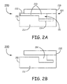
- MEMS device 200 illustrated in Figures 2A and 2B .
- MEMS device 200 is intended to generically represent MEMS devices rather than any specific MEMS device or class of MEMS devices. That is, the method shown in Figure 1 is intended to cover in scope embodiments for fabricating any MEMS device designs calling for open areas (i.e. voids) within the structure of the device.
- open areas i.e. voids
- the method begins at 110 with applying a patterned layer of Aerogel material onto a substrate to form an Aerogel sacrificial layer.
- a sacrificial layer 220 of Aerogel material is applied onto a substrate 210 at one of more locations where a void is called for per the MEMS device 200 design.
- the substrate 210 may include indented regions 211 which are at least partially filled when the pattered layer of Aerogel material is applied.
- the substrate 210 is a silicon or other material that forms a non-sacrificial layer of the MEMS device 200.
- the substrate 210 itself may comprise a combination of non-sacrificial material 212 and a previously applied sacrificial layer 214 of Aerogel material.
- Sacrificial layer 220 provides a structural foundation for building additional structures onto substrate 210.
- the density and pore size for the Aerogel material can be separately controlled by one of ordinary skill in the art upon reading this specification using known processes and standards for spin coating Aerogel layers.
- the method proceeds at 120 with applying at least one non-sacrificial Silicon layer 230 over the Aerogel sacrificial layer 220.
- the sacrificial layer 220 was patterned so that the subsequently applied non-sacrificial silicon layers 230 will contact with, and thus remain secured to, substrate 210 once sacrificial layer 220 is removed. That is, if sacrificial layer 220 were applied as a continuous film over substrate 210, then when sacrificial layer 220 is removed non-sacrificial silicon layers 230 and any structures above it would simply lift off. Thus one or more gaps in the patterned layer of Aerogel material laid over substrate 210 are provided for attaching the subsequently applied non-sacrificial silicon layers 230 to substrate 210 (shown generally at 222).
- the method optionally provides for applying a protection layer 222 to one or more exposed portions 224 of the Aerogel sacrificial layer 220 (shown in blocks 140 and 140').
- Protection layer 222 may be applied prior to applying non-sacrificial silicon layer 230 over the Aerogel sacrificial layer 220 (indicated by block 140), or after (indicated by block 140'), based on when the presence of such liquids is expected during fabrication. For fabrication processes where liquids will not be present prior to removal of Aerogel sacrificial layer 220, application of protection layer 222 may not be necessary, and for that reason is optional.
- the method proceeds at 150 with removing the Aerogel sacrificial layer 220 by exposing the Aerogel sacrificial layer 220 to a removal liquid.
- removing the Aerogel sacrificial layer 220 will include the additional step of breaching the protection layer 222 in the desired places to allow the removal liquid to reach Aerogel sacrificial layer 220 (indicated by block 145).
- Figure 2B provides a diagram of MEMS device 220 with sacrificial layers 220 and 214 removed to open up void 290.
- the Aerogel sacrificial layer 220 is removed by introducing a chemical etchant that dissolves the Aerogel material.
- a chemical etchant is appropriate for embodiments where Aerogel sacrificial layer 220 needs to be dissolved and the waste products removed (to prevent potential interference with moving parts, for example).
- appropriate chemical etchants include, but are not limited to hydrofluoric acid, phosphoric acid or organic solvents. Because of the low density and porous structure of the Aerogel material, there is less physical mass to dissolve meaning that relatively less chemical etchant is necessary per unit volume. Further, because there is relatively less waste material produced, there is less waste material to inhibit flow of fresh etchant into the void and less waste material that needs to be removed. Since only the solid part of the Aerogel must be dissolved, the sacrificial etch will be faster, limiting any small but finite etching of the non-sacrificial materials.
- the Aerogel sacrificial layer 220 is removed by introducing an inert chemical that collapses the Aerogel material.
- an inert chemical is appropriate for embodiments where having a small amount of waste material remaining in the void is acceptable and will not interfere with other structures (for example, where the void created by removing the Aerogel sacrificial layer 220 will be used as a fluid conduit).
- the inert chemical will not appreciably dissolve the Aerogel material. However, the surface tension of the liquid will cause the Aerogel material to collapse, thus opening a void within MEMS device 200 where the Aerogel sacrificial layer 220 previously existed.
- appropriate inert chemicals include, but are not limited to, alcohols, acetone, or water. Whether a chemical is considered inert with respect to the remaining structures of the MEMS device 200 can be readily determined by one of ordinary skill in the art upon reading this specification based on the chemical properties of said remaining structures.
- Aerogel sacrificial layer 220 has been removed to open up the desired voids in MEMS device 200, further process should be avoided so as not to damage moving parts within the voids or introduce foreign material contaminants.
Landscapes
- Engineering & Computer Science (AREA)
- Manufacturing & Machinery (AREA)
- Chemical & Material Sciences (AREA)
- Analytical Chemistry (AREA)
- Microelectronics & Electronic Packaging (AREA)
- Micromachines (AREA)
Applications Claiming Priority (1)
| Application Number | Priority Date | Filing Date | Title |
|---|---|---|---|
| US12/940,348 US8293657B2 (en) | 2010-11-05 | 2010-11-05 | Sacrificial layers made from aerogel for microelectromechanical systems (MEMS) device fabrication processes |
Publications (3)
| Publication Number | Publication Date |
|---|---|
| EP2450309A2 true EP2450309A2 (de) | 2012-05-09 |
| EP2450309A3 EP2450309A3 (de) | 2014-04-30 |
| EP2450309B1 EP2450309B1 (de) | 2016-01-27 |
Family
ID=45033754
Family Applications (1)
| Application Number | Title | Priority Date | Filing Date |
|---|---|---|---|
| EP11187357.6A Not-in-force EP2450309B1 (de) | 2010-11-05 | 2011-10-31 | Opferschichten aus Aerogel für die Herstellung von MEMS-Vorrichtungen |
Country Status (3)
| Country | Link |
|---|---|
| US (1) | US8293657B2 (de) |
| EP (1) | EP2450309B1 (de) |
| JP (1) | JP2012101351A (de) |
Families Citing this family (1)
| Publication number | Priority date | Publication date | Assignee | Title |
|---|---|---|---|---|
| US12330933B2 (en) | 2022-12-20 | 2025-06-17 | xMEMS Labs, Inc. | Cantilever structure with intermediate substrate connection having a film with on anchor with protrusion |
Citations (1)
| Publication number | Priority date | Publication date | Assignee | Title |
|---|---|---|---|---|
| US20090184088A1 (en) | 2008-01-22 | 2009-07-23 | Honeywell International, Inc | Aerogel-Bases Mold for MEMS Fabrication and Formation Thereof |
Family Cites Families (19)
| Publication number | Priority date | Publication date | Assignee | Title |
|---|---|---|---|---|
| US5409683A (en) | 1990-08-23 | 1995-04-25 | Regents Of The University Of California | Method for producing metal oxide aerogels |
| US5658832A (en) | 1994-10-17 | 1997-08-19 | Regents Of The University Of California | Method of forming a spacer for field emission flat panel displays |
| JP4000615B2 (ja) * | 1997-03-21 | 2007-10-31 | 日産自動車株式会社 | 微小機械の製造方法 |
| US5973015A (en) | 1998-02-02 | 1999-10-26 | The Regents Of The University Of California | Flexible aerogel composite for mechanical stability and process of fabrication |
| US6168737B1 (en) | 1998-02-23 | 2001-01-02 | The Regents Of The University Of California | Method of casting patterned dielectric structures |
| DE19911847A1 (de) | 1999-03-17 | 2000-09-28 | Deutsch Zentr Luft & Raumfahrt | Fein- und Formguß in Kunststoff/Kohlenstoff-Aerogelen |
| JP3751778B2 (ja) | 1999-04-26 | 2006-03-01 | 日本板硝子株式会社 | ゾルゲル成形物の製造方法 |
| JP2001240800A (ja) | 2000-02-25 | 2001-09-04 | Nippon Sheet Glass Co Ltd | 所定表面形状を有する物品の製造方法 |
| US6270846B1 (en) | 2000-03-02 | 2001-08-07 | Sandia Corporation | Method for making surfactant-templated, high-porosity thin films |
| US6422528B1 (en) | 2001-01-17 | 2002-07-23 | Sandia National Laboratories | Sacrificial plastic mold with electroplatable base |
| US6620458B2 (en) | 2001-09-27 | 2003-09-16 | The Regents Of The University Of California | Method to produce alumina aerogels having porosities greater than 80 percent |
| EP1398831A3 (de) * | 2002-09-13 | 2008-02-20 | Shipley Co. L.L.C. | Bildung von Luftspalten |
| US7150844B2 (en) | 2003-10-16 | 2006-12-19 | Seagate Technology Llc | Dry passivation process for stamper/imprinter family making for patterned recording media |
| US7226146B2 (en) * | 2004-11-30 | 2007-06-05 | Xerox Corporation | Fluid ejection devices and methods for forming such devices |
| US7479404B2 (en) | 2005-07-08 | 2009-01-20 | The Board Of Trustees Of The University Of Illinois | Photonic crystal biosensor structure and fabrication method |
| US7450295B2 (en) | 2006-03-02 | 2008-11-11 | Qualcomm Mems Technologies, Inc. | Methods for producing MEMS with protective coatings using multi-component sacrificial layers |
| JP4940784B2 (ja) | 2006-06-28 | 2012-05-30 | 凸版印刷株式会社 | インプリント用モールドおよびインプリント用モールド製造方法 |
| US8318253B2 (en) | 2006-06-30 | 2012-11-27 | Asml Netherlands B.V. | Imprint lithography |
| JP5115402B2 (ja) * | 2008-08-29 | 2013-01-09 | 富士通株式会社 | 可変キャパシタおよび可変キャパシタ製造方法 |
-
2010
- 2010-11-05 US US12/940,348 patent/US8293657B2/en not_active Expired - Fee Related
-
2011
- 2011-10-31 EP EP11187357.6A patent/EP2450309B1/de not_active Not-in-force
- 2011-11-04 JP JP2011242341A patent/JP2012101351A/ja not_active Ceased
Patent Citations (1)
| Publication number | Priority date | Publication date | Assignee | Title |
|---|---|---|---|---|
| US20090184088A1 (en) | 2008-01-22 | 2009-07-23 | Honeywell International, Inc | Aerogel-Bases Mold for MEMS Fabrication and Formation Thereof |
Also Published As
| Publication number | Publication date |
|---|---|
| JP2012101351A (ja) | 2012-05-31 |
| US8293657B2 (en) | 2012-10-23 |
| EP2450309A3 (de) | 2014-04-30 |
| US20120115269A1 (en) | 2012-05-10 |
| EP2450309B1 (de) | 2016-01-27 |
Similar Documents
| Publication | Publication Date | Title |
|---|---|---|
| KR100421217B1 (ko) | 점착 방지 미세 구조물 제조 방법 | |
| US7276277B2 (en) | Micromechanical component, in particular a sensor element, having a stabilized membrane and a method of producing such a component | |
| JP6235023B2 (ja) | シリコンエッチング法 | |
| JP2008072091A5 (de) | ||
| TW201203311A (en) | Method for forming contact hole of semiconductor device | |
| US7811938B2 (en) | Method for forming gaps in micromechanical device and micromechanical device | |
| KR100237000B1 (ko) | 희생층을 사용한 미소구조체 제조 방법 | |
| US20060194404A1 (en) | Method and system for fabricating and cleaning free-standing nanostructures | |
| US7976714B2 (en) | Single SOI wafer accelerometer fabrication process | |
| US8293657B2 (en) | Sacrificial layers made from aerogel for microelectromechanical systems (MEMS) device fabrication processes | |
| US20140252512A1 (en) | Methods And Apparatus For MEMS Structure Release | |
| CN102375332B (zh) | 一种用于mems结构的悬架光刻胶平坦化工艺 | |
| US8330238B2 (en) | Microscopic structure packaging method and device with packaged microscopic structure | |
| Pérez-Díaz et al. | Silicon microstructures through the production of silicon nanowires by metal-assisted chemical etching, used as sacrificial material | |
| CN113495430B (zh) | 一种光刻胶图案化方法及光刻胶剥离方法 | |
| EP3397587B1 (de) | System und verfahren zur bewahrung einer geglätteten oberfläche auf einer mems-vorrichtung | |
| US20070196998A1 (en) | System and method for forming moveable features on a composite substrate | |
| CN210193393U (zh) | 一种mems结构 | |
| TWI565333B (zh) | 用於釋放微機電系統(mems)裝置中的隔膜的方法 | |
| EP2695848A1 (de) | Integrierte Schaltung mit MEMS-Element gestaltet um Festhaften zu vermeiden und Herstellungsverfahren dafür | |
| Sandoughsaz et al. | Realization of complex three-dimensional free-standing structures on silicon substrates using controllable underetching in a deep reactive ion etching | |
| TWI606007B (zh) | 採用複合基材的微機電元件以及其製作方法 | |
| DE102012213305A1 (de) | Verfahren zur Herstellung eines MEMS-Bauelements mit einer Membranstruktur und Bauteil mit einem solchen MEMS-Bauelement | |
| KR100836505B1 (ko) | 반도체 소자의 절연막을 식각하는 방법 | |
| KR100865911B1 (ko) | 미세 구조물 제조방법 |
Legal Events
| Date | Code | Title | Description |
|---|---|---|---|
| PUAI | Public reference made under article 153(3) epc to a published international application that has entered the european phase |
Free format text: ORIGINAL CODE: 0009012 |
|
| 17P | Request for examination filed |
Effective date: 20111031 |
|
| AK | Designated contracting states |
Kind code of ref document: A2 Designated state(s): AL AT BE BG CH CY CZ DE DK EE ES FI FR GB GR HR HU IE IS IT LI LT LU LV MC MK MT NL NO PL PT RO RS SE SI SK SM TR |
|
| AX | Request for extension of the european patent |
Extension state: BA ME |
|
| PUAL | Search report despatched |
Free format text: ORIGINAL CODE: 0009013 |
|
| AK | Designated contracting states |
Kind code of ref document: A3 Designated state(s): AL AT BE BG CH CY CZ DE DK EE ES FI FR GB GR HR HU IE IS IT LI LT LU LV MC MK MT NL NO PL PT RO RS SE SI SK SM TR |
|
| AX | Request for extension of the european patent |
Extension state: BA ME |
|
| RIC1 | Information provided on ipc code assigned before grant |
Ipc: B81C 1/00 20060101AFI20140326BHEP |
|
| 17Q | First examination report despatched |
Effective date: 20140512 |
|
| GRAP | Despatch of communication of intention to grant a patent |
Free format text: ORIGINAL CODE: EPIDOSNIGR1 |
|
| INTG | Intention to grant announced |
Effective date: 20151007 |
|
| GRAS | Grant fee paid |
Free format text: ORIGINAL CODE: EPIDOSNIGR3 |
|
| RAP1 | Party data changed (applicant data changed or rights of an application transferred) |
Owner name: HONEYWELL INTERNATIONAL INC. |
|
| GRAA | (expected) grant |
Free format text: ORIGINAL CODE: 0009210 |
|
| AK | Designated contracting states |
Kind code of ref document: B1 Designated state(s): AL AT BE BG CH CY CZ DE DK EE ES FI FR GB GR HR HU IE IS IT LI LT LU LV MC MK MT NL NO PL PT RO RS SE SI SK SM TR |
|
| REG | Reference to a national code |
Ref country code: GB Ref legal event code: FG4D |
|
| REG | Reference to a national code |
Ref country code: CH Ref legal event code: EP |
|
| REG | Reference to a national code |
Ref country code: AT Ref legal event code: REF Ref document number: 772593 Country of ref document: AT Kind code of ref document: T Effective date: 20160215 |
|
| REG | Reference to a national code |
Ref country code: IE Ref legal event code: FG4D |
|
| REG | Reference to a national code |
Ref country code: DE Ref legal event code: R096 Ref document number: 602011022961 Country of ref document: DE |
|
| REG | Reference to a national code |
Ref country code: LT Ref legal event code: MG4D |
|
| REG | Reference to a national code |
Ref country code: NL Ref legal event code: MP Effective date: 20160127 |
|
| REG | Reference to a national code |
Ref country code: AT Ref legal event code: MK05 Ref document number: 772593 Country of ref document: AT Kind code of ref document: T Effective date: 20160127 |
|
| PG25 | Lapsed in a contracting state [announced via postgrant information from national office to epo] |
Ref country code: NL Free format text: LAPSE BECAUSE OF FAILURE TO SUBMIT A TRANSLATION OF THE DESCRIPTION OR TO PAY THE FEE WITHIN THE PRESCRIBED TIME-LIMIT Effective date: 20160127 |
|
| PG25 | Lapsed in a contracting state [announced via postgrant information from national office to epo] |
Ref country code: HR Free format text: LAPSE BECAUSE OF FAILURE TO SUBMIT A TRANSLATION OF THE DESCRIPTION OR TO PAY THE FEE WITHIN THE PRESCRIBED TIME-LIMIT Effective date: 20160127 Ref country code: ES Free format text: LAPSE BECAUSE OF FAILURE TO SUBMIT A TRANSLATION OF THE DESCRIPTION OR TO PAY THE FEE WITHIN THE PRESCRIBED TIME-LIMIT Effective date: 20160127 Ref country code: FI Free format text: LAPSE BECAUSE OF FAILURE TO SUBMIT A TRANSLATION OF THE DESCRIPTION OR TO PAY THE FEE WITHIN THE PRESCRIBED TIME-LIMIT Effective date: 20160127 Ref country code: GR Free format text: LAPSE BECAUSE OF FAILURE TO SUBMIT A TRANSLATION OF THE DESCRIPTION OR TO PAY THE FEE WITHIN THE PRESCRIBED TIME-LIMIT Effective date: 20160428 Ref country code: IT Free format text: LAPSE BECAUSE OF FAILURE TO SUBMIT A TRANSLATION OF THE DESCRIPTION OR TO PAY THE FEE WITHIN THE PRESCRIBED TIME-LIMIT Effective date: 20160127 Ref country code: NO Free format text: LAPSE BECAUSE OF FAILURE TO SUBMIT A TRANSLATION OF THE DESCRIPTION OR TO PAY THE FEE WITHIN THE PRESCRIBED TIME-LIMIT Effective date: 20160427 |
|
| PG25 | Lapsed in a contracting state [announced via postgrant information from national office to epo] |
Ref country code: SE Free format text: LAPSE BECAUSE OF FAILURE TO SUBMIT A TRANSLATION OF THE DESCRIPTION OR TO PAY THE FEE WITHIN THE PRESCRIBED TIME-LIMIT Effective date: 20160127 Ref country code: AT Free format text: LAPSE BECAUSE OF FAILURE TO SUBMIT A TRANSLATION OF THE DESCRIPTION OR TO PAY THE FEE WITHIN THE PRESCRIBED TIME-LIMIT Effective date: 20160127 Ref country code: PT Free format text: LAPSE BECAUSE OF FAILURE TO SUBMIT A TRANSLATION OF THE DESCRIPTION OR TO PAY THE FEE WITHIN THE PRESCRIBED TIME-LIMIT Effective date: 20160527 Ref country code: RS Free format text: LAPSE BECAUSE OF FAILURE TO SUBMIT A TRANSLATION OF THE DESCRIPTION OR TO PAY THE FEE WITHIN THE PRESCRIBED TIME-LIMIT Effective date: 20160127 Ref country code: IS Free format text: LAPSE BECAUSE OF FAILURE TO SUBMIT A TRANSLATION OF THE DESCRIPTION OR TO PAY THE FEE WITHIN THE PRESCRIBED TIME-LIMIT Effective date: 20160527 Ref country code: LV Free format text: LAPSE BECAUSE OF FAILURE TO SUBMIT A TRANSLATION OF THE DESCRIPTION OR TO PAY THE FEE WITHIN THE PRESCRIBED TIME-LIMIT Effective date: 20160127 Ref country code: LT Free format text: LAPSE BECAUSE OF FAILURE TO SUBMIT A TRANSLATION OF THE DESCRIPTION OR TO PAY THE FEE WITHIN THE PRESCRIBED TIME-LIMIT Effective date: 20160127 Ref country code: PL Free format text: LAPSE BECAUSE OF FAILURE TO SUBMIT A TRANSLATION OF THE DESCRIPTION OR TO PAY THE FEE WITHIN THE PRESCRIBED TIME-LIMIT Effective date: 20160127 |
|
| REG | Reference to a national code |
Ref country code: DE Ref legal event code: R097 Ref document number: 602011022961 Country of ref document: DE |
|
| PG25 | Lapsed in a contracting state [announced via postgrant information from national office to epo] |
Ref country code: EE Free format text: LAPSE BECAUSE OF FAILURE TO SUBMIT A TRANSLATION OF THE DESCRIPTION OR TO PAY THE FEE WITHIN THE PRESCRIBED TIME-LIMIT Effective date: 20160127 Ref country code: DK Free format text: LAPSE BECAUSE OF FAILURE TO SUBMIT A TRANSLATION OF THE DESCRIPTION OR TO PAY THE FEE WITHIN THE PRESCRIBED TIME-LIMIT Effective date: 20160127 |
|
| PG25 | Lapsed in a contracting state [announced via postgrant information from national office to epo] |
Ref country code: SM Free format text: LAPSE BECAUSE OF FAILURE TO SUBMIT A TRANSLATION OF THE DESCRIPTION OR TO PAY THE FEE WITHIN THE PRESCRIBED TIME-LIMIT Effective date: 20160127 Ref country code: RO Free format text: LAPSE BECAUSE OF FAILURE TO SUBMIT A TRANSLATION OF THE DESCRIPTION OR TO PAY THE FEE WITHIN THE PRESCRIBED TIME-LIMIT Effective date: 20160127 Ref country code: SK Free format text: LAPSE BECAUSE OF FAILURE TO SUBMIT A TRANSLATION OF THE DESCRIPTION OR TO PAY THE FEE WITHIN THE PRESCRIBED TIME-LIMIT Effective date: 20160127 Ref country code: CZ Free format text: LAPSE BECAUSE OF FAILURE TO SUBMIT A TRANSLATION OF THE DESCRIPTION OR TO PAY THE FEE WITHIN THE PRESCRIBED TIME-LIMIT Effective date: 20160127 |
|
| PLBE | No opposition filed within time limit |
Free format text: ORIGINAL CODE: 0009261 |
|
| STAA | Information on the status of an ep patent application or granted ep patent |
Free format text: STATUS: NO OPPOSITION FILED WITHIN TIME LIMIT |
|
| PG25 | Lapsed in a contracting state [announced via postgrant information from national office to epo] |
Ref country code: BE Free format text: LAPSE BECAUSE OF FAILURE TO SUBMIT A TRANSLATION OF THE DESCRIPTION OR TO PAY THE FEE WITHIN THE PRESCRIBED TIME-LIMIT Effective date: 20160127 |
|
| 26N | No opposition filed |
Effective date: 20161028 |
|
| PG25 | Lapsed in a contracting state [announced via postgrant information from national office to epo] |
Ref country code: BG Free format text: LAPSE BECAUSE OF FAILURE TO SUBMIT A TRANSLATION OF THE DESCRIPTION OR TO PAY THE FEE WITHIN THE PRESCRIBED TIME-LIMIT Effective date: 20160427 Ref country code: SI Free format text: LAPSE BECAUSE OF FAILURE TO SUBMIT A TRANSLATION OF THE DESCRIPTION OR TO PAY THE FEE WITHIN THE PRESCRIBED TIME-LIMIT Effective date: 20160127 |
|
| REG | Reference to a national code |
Ref country code: DE Ref legal event code: R119 Ref document number: 602011022961 Country of ref document: DE |
|
| REG | Reference to a national code |
Ref country code: CH Ref legal event code: PL |
|
| GBPC | Gb: european patent ceased through non-payment of renewal fee |
Effective date: 20161031 |
|
| REG | Reference to a national code |
Ref country code: IE Ref legal event code: MM4A |
|
| REG | Reference to a national code |
Ref country code: FR Ref legal event code: ST Effective date: 20170630 |
|
| PG25 | Lapsed in a contracting state [announced via postgrant information from national office to epo] |
Ref country code: CH Free format text: LAPSE BECAUSE OF NON-PAYMENT OF DUE FEES Effective date: 20161031 Ref country code: FR Free format text: LAPSE BECAUSE OF NON-PAYMENT OF DUE FEES Effective date: 20161102 Ref country code: LI Free format text: LAPSE BECAUSE OF NON-PAYMENT OF DUE FEES Effective date: 20161031 Ref country code: GB Free format text: LAPSE BECAUSE OF NON-PAYMENT OF DUE FEES Effective date: 20161031 Ref country code: DE Free format text: LAPSE BECAUSE OF NON-PAYMENT OF DUE FEES Effective date: 20170503 |
|
| PG25 | Lapsed in a contracting state [announced via postgrant information from national office to epo] |
Ref country code: LU Free format text: LAPSE BECAUSE OF NON-PAYMENT OF DUE FEES Effective date: 20161031 |
|
| PG25 | Lapsed in a contracting state [announced via postgrant information from national office to epo] |
Ref country code: IE Free format text: LAPSE BECAUSE OF NON-PAYMENT OF DUE FEES Effective date: 20161031 |
|
| PG25 | Lapsed in a contracting state [announced via postgrant information from national office to epo] |
Ref country code: HU Free format text: LAPSE BECAUSE OF FAILURE TO SUBMIT A TRANSLATION OF THE DESCRIPTION OR TO PAY THE FEE WITHIN THE PRESCRIBED TIME-LIMIT; INVALID AB INITIO Effective date: 20111031 Ref country code: CY Free format text: LAPSE BECAUSE OF FAILURE TO SUBMIT A TRANSLATION OF THE DESCRIPTION OR TO PAY THE FEE WITHIN THE PRESCRIBED TIME-LIMIT Effective date: 20160127 |
|
| PG25 | Lapsed in a contracting state [announced via postgrant information from national office to epo] |
Ref country code: MC Free format text: LAPSE BECAUSE OF FAILURE TO SUBMIT A TRANSLATION OF THE DESCRIPTION OR TO PAY THE FEE WITHIN THE PRESCRIBED TIME-LIMIT Effective date: 20160127 Ref country code: MT Free format text: LAPSE BECAUSE OF NON-PAYMENT OF DUE FEES Effective date: 20161031 Ref country code: MK Free format text: LAPSE BECAUSE OF FAILURE TO SUBMIT A TRANSLATION OF THE DESCRIPTION OR TO PAY THE FEE WITHIN THE PRESCRIBED TIME-LIMIT Effective date: 20160127 Ref country code: TR Free format text: LAPSE BECAUSE OF FAILURE TO SUBMIT A TRANSLATION OF THE DESCRIPTION OR TO PAY THE FEE WITHIN THE PRESCRIBED TIME-LIMIT Effective date: 20160127 |
|
| PG25 | Lapsed in a contracting state [announced via postgrant information from national office to epo] |
Ref country code: AL Free format text: LAPSE BECAUSE OF FAILURE TO SUBMIT A TRANSLATION OF THE DESCRIPTION OR TO PAY THE FEE WITHIN THE PRESCRIBED TIME-LIMIT Effective date: 20160127 |
|
| P01 | Opt-out of the competence of the unified patent court (upc) registered |
Effective date: 20230525 |