EP2448014A2 - Lichtemittierendes Halbleiterbauelement - Google Patents
Lichtemittierendes Halbleiterbauelement Download PDFInfo
- Publication number
- EP2448014A2 EP2448014A2 EP20110180652 EP11180652A EP2448014A2 EP 2448014 A2 EP2448014 A2 EP 2448014A2 EP 20110180652 EP20110180652 EP 20110180652 EP 11180652 A EP11180652 A EP 11180652A EP 2448014 A2 EP2448014 A2 EP 2448014A2
- Authority
- EP
- European Patent Office
- Prior art keywords
- electrode
- disposed
- insulating part
- conductive
- electrically connected
- Prior art date
- Legal status (The legal status is an assumption and is not a legal conclusion. Google has not performed a legal analysis and makes no representation as to the accuracy of the status listed.)
- Granted
Links
Images


Classifications
-
- H—ELECTRICITY
- H10—SEMICONDUCTOR DEVICES; ELECTRIC SOLID-STATE DEVICES NOT OTHERWISE PROVIDED FOR
- H10H—INORGANIC LIGHT-EMITTING SEMICONDUCTOR DEVICES HAVING POTENTIAL BARRIERS
- H10H20/00—Individual inorganic light-emitting semiconductor devices having potential barriers, e.g. light-emitting diodes [LED]
- H10H20/80—Constructional details
- H10H20/83—Electrodes
- H10H20/831—Electrodes characterised by their shape
-
- H—ELECTRICITY
- H10—SEMICONDUCTOR DEVICES; ELECTRIC SOLID-STATE DEVICES NOT OTHERWISE PROVIDED FOR
- H10H—INORGANIC LIGHT-EMITTING SEMICONDUCTOR DEVICES HAVING POTENTIAL BARRIERS
- H10H20/00—Individual inorganic light-emitting semiconductor devices having potential barriers, e.g. light-emitting diodes [LED]
- H10H20/80—Constructional details
- H10H20/81—Bodies
- H10H20/819—Bodies characterised by their shape, e.g. curved or truncated substrates
-
- H—ELECTRICITY
- H10—SEMICONDUCTOR DEVICES; ELECTRIC SOLID-STATE DEVICES NOT OTHERWISE PROVIDED FOR
- H10H—INORGANIC LIGHT-EMITTING SEMICONDUCTOR DEVICES HAVING POTENTIAL BARRIERS
- H10H20/00—Individual inorganic light-emitting semiconductor devices having potential barriers, e.g. light-emitting diodes [LED]
- H10H20/80—Constructional details
- H10H20/83—Electrodes
- H10H20/831—Electrodes characterised by their shape
- H10H20/8312—Electrodes characterised by their shape extending at least partially through the bodies
-
- H—ELECTRICITY
- H10—SEMICONDUCTOR DEVICES; ELECTRIC SOLID-STATE DEVICES NOT OTHERWISE PROVIDED FOR
- H10H—INORGANIC LIGHT-EMITTING SEMICONDUCTOR DEVICES HAVING POTENTIAL BARRIERS
- H10H20/00—Individual inorganic light-emitting semiconductor devices having potential barriers, e.g. light-emitting diodes [LED]
- H10H20/80—Constructional details
- H10H20/83—Electrodes
- H10H20/831—Electrodes characterised by their shape
- H10H20/8316—Multi-layer electrodes comprising at least one discontinuous layer
-
- H—ELECTRICITY
- H10—SEMICONDUCTOR DEVICES; ELECTRIC SOLID-STATE DEVICES NOT OTHERWISE PROVIDED FOR
- H10H—INORGANIC LIGHT-EMITTING SEMICONDUCTOR DEVICES HAVING POTENTIAL BARRIERS
- H10H20/00—Individual inorganic light-emitting semiconductor devices having potential barriers, e.g. light-emitting diodes [LED]
- H10H20/80—Constructional details
- H10H20/83—Electrodes
- H10H20/832—Electrodes characterised by their material
- H10H20/833—Transparent materials
-
- H—ELECTRICITY
- H10—SEMICONDUCTOR DEVICES; ELECTRIC SOLID-STATE DEVICES NOT OTHERWISE PROVIDED FOR
- H10H—INORGANIC LIGHT-EMITTING SEMICONDUCTOR DEVICES HAVING POTENTIAL BARRIERS
- H10H20/00—Individual inorganic light-emitting semiconductor devices having potential barriers, e.g. light-emitting diodes [LED]
- H10H20/80—Constructional details
- H10H20/84—Coatings, e.g. passivation layers or antireflective coatings
-
- H—ELECTRICITY
- H10—SEMICONDUCTOR DEVICES; ELECTRIC SOLID-STATE DEVICES NOT OTHERWISE PROVIDED FOR
- H10H—INORGANIC LIGHT-EMITTING SEMICONDUCTOR DEVICES HAVING POTENTIAL BARRIERS
- H10H20/00—Individual inorganic light-emitting semiconductor devices having potential barriers, e.g. light-emitting diodes [LED]
- H10H20/80—Constructional details
- H10H20/85—Packages
- H10H20/857—Interconnections, e.g. lead-frames, bond wires or solder balls
-
- H—ELECTRICITY
- H10—SEMICONDUCTOR DEVICES; ELECTRIC SOLID-STATE DEVICES NOT OTHERWISE PROVIDED FOR
- H10H—INORGANIC LIGHT-EMITTING SEMICONDUCTOR DEVICES HAVING POTENTIAL BARRIERS
- H10H29/00—Integrated devices, or assemblies of multiple devices, comprising at least one light-emitting semiconductor element covered by group H10H20/00
- H10H29/10—Integrated devices comprising at least one light-emitting semiconductor component covered by group H10H20/00
- H10H29/14—Integrated devices comprising at least one light-emitting semiconductor component covered by group H10H20/00 comprising multiple light-emitting semiconductor components
-
- H—ELECTRICITY
- H10—SEMICONDUCTOR DEVICES; ELECTRIC SOLID-STATE DEVICES NOT OTHERWISE PROVIDED FOR
- H10H—INORGANIC LIGHT-EMITTING SEMICONDUCTOR DEVICES HAVING POTENTIAL BARRIERS
- H10H20/00—Individual inorganic light-emitting semiconductor devices having potential barriers, e.g. light-emitting diodes [LED]
- H10H20/80—Constructional details
- H10H20/81—Bodies
- H10H20/813—Bodies having a plurality of light-emitting regions, e.g. multi-junction LEDs or light-emitting devices having photoluminescent regions within the bodies
Definitions
- the present invention relates to a semiconductor light emitting device.
- a light emitting diode a type of semiconductor light emitting device, is a semiconductor device capable of generating light of various colors according to electron hole recombination in p and n type semiconductor junction parts when current is applied thereto.
- the semiconductor light emitting device Compared with a light emitting device based on a filament, the semiconductor light emitting device has various advantages such as a long life span, low power consumption, excellent initial driving characteristics, high vibration resistance, and the like, so demand for the semiconductor light emitting device continues to grow.
- a group III-nitride semiconductor capable of emitting short-wavelength blue light has come to prominence.
- electrodes are generally arranged in a horizontal direction, narrowing a current flow.
- the narrow current flow increases an operation voltage Vf of the light emitting device, degrading current efficiency, and in addition, the light emitting device may become vulnerable to an electrostatic discharge.
- the electrodes are divided into pads and fingers and disposed thusly.
- an active layer is etched to expose a first conductive semiconductor layer, and a first pad and finger are formed on the first conductive semiconductor layer and a second pad and finger are formed on a second conductive semiconductor layer.
- the area of the active layer is reduced and a uniform space between the electrodes cannot be secured to cause non-uniform current spreading.
- the object of the present invention is to obtain uniform current spreading by maintaining a uniform interval between the electrodes of a semiconductor light emitting device, and improve the luminance of the semiconductor light emitting device by avoiding a loss of (i.e., reduction in) an active layer resulting from etching.
- An aspect of the present invention provides a semiconductor light emitting device having electrodes for minimizing a loss of light and improving a current spreading effect.
- a semiconductor light emitting device including: a first conductive semiconductor layer including first and second areas; an active layer disposed on the second area; a second conductive semiconductor layer disposed on the active layer; first and second electrode branches disposed on the first and second conductive semiconductor layers, respectively; a first electrode pad electrically connected to the first electrode branch and disposed on the first electrode branch; and a second electrode pad electrically connected to the second electrode branch and disposed on the second electrode branch.
- the first and second areas may have a stripe shape.
- the first and second electrode branches may have a stripe shape.
- a plurality of first and second electrode branches may be disposed and alternately formed.
- the semiconductor light emitting device may further include: an insulating part formed on the first and second conductive semiconductor layers.
- the insulating part may allow at least a portion of each of upper surfaces of the first and second electrode branches to be exposed.
- the first and second electrode pads may be disposed on the exposed portions of the upper surfaces of the first and second electrode branches, respectively.
- the insulating part may cover the upper portions of the first and second electrode branches, and at least one first conductive via electrically connected to the first electrode branch and at least one second conductive via electrically connected to the second electrode branch may be penetratingly formed through portions of the insulating part in a thicknesswise direction.
- the first and second conductive vias may be penetratingly formed through the insulating part in a vertical direction.
- the first and second electrode pads may be disposed on the insulating part, and the first electrode pad may be electrically connected to the first electrode branch through the first conductive via, and the second electrode pad may be electrically connected to the second electrode branch through the second conductive via.
- the semiconductor light emitting device may further include: a first connection part extending from the first electrode pad to the first conductive via along the upper surface of the insulating part, and a second connection part extending from the second electrode pad to the second conductive via along the upper surface of the insulating part.
- At least one of the first and second connection parts may be provided as a plurality of connection parts.
- the first connection part may be connected to the plurality of first conductive vias, and the second connection part may be connected to the plurality of second conductive vias.
- the upper surface of the insulating part may have a rectangular shape, and the first conductive vias may be arranged along one side of the upper surface of the insulating part and the second conductive vias may be arranged along the other side opposed to the one side.
- the upper surface of the insulating part may have a rectangular shape, and the second electrode pads may be disposed to be adjacent to one corner and neighboring another corner of the upper surface of the insulating part, and the first electrode pad may be disposed at a position spaced apart by the same distance from the respective second electrode pads.
- the insulating part may be formed to include a silicon oxide.
- the semiconductor light emitting device may further include: a transparent electrode layer formed on the upper surface of the second conductive semiconductor layer.
- the second electrode branch may be disposed on an upper surface of the transparent electrode layer.
- At least one of the first and second electrode pads may be disposed as a plurality of electrode pads.
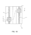
- FIGS. 1a and 1b are a schematic sectional view and a plan view of a semiconductor light emitting device according to an exemplary embodiment of the present invention
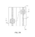
- FIGS. 2a and 2b are a schematic sectional view and a plan view of a semiconductor light emitting device according to an exemplary embodiment of the present invention
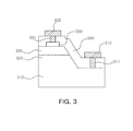
- FIG. 3 is a schematic sectional view of a semiconductor light emitting device according to another exemplary embodiment of the present invention.
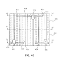
- FIGS. 4a to 4e are a schematic perspective view, a plan view, and a sectional view showing a semiconductor light emitting device according to another exemplary embodiment of the present invention.
- FIGS. 1a and 1b are a schematic sectional view and a plan view of a semiconductor light emitting device according to an exemplary embodiment of the present invention. Specifically, FIG. 1a is a sectional view taken along line X-X' in FIG. 1b .
- a semiconductor light emitting device includes a first conductive semiconductor layer 110 including first and second areas, an active layer 120 disposed on the second area, a second conductive semiconductor layer 130 disposed on the active layer 120, first and second electrode branches 111 and 131 respectively disposed on the first and second conductive semiconductor layers 110 and 130, a first electrode pad 112 electrically connected to the first electrode branch 111 and disposed to be separated from the first conductive semiconductor layer 110, a second electrode pad 132 electrically connected to the second electrode branch 131 and disposed to be separated from the second conductive semiconductor layer 130, and an insulating part 140 formed on the first and second conductive semiconductor layers 110 and 130.
- the respective elements and their connective relationships within the semiconductor light emitting device according to the present exemplary embodiment will be described in detail with reference to the accompanying drawings.
- the first area may be defined as an area of the first conductive semiconductor layer 110 exposed by removing a portion of the light emission structure, and the second area may be defined as the other remaining area, excluding the first area.
- This configuration can be obtained through a process of selectively etching a portion of the light emission structure as could be easily understood by a person skilled in the art to which the present invention pertains.
- the first and second conductive semiconductor layers 110 and 130 may be made of a nitride semiconductor, specifically, a material expressed by an empirical formula Al x In y Ga( 1-x-y )N (Here, 0 ⁇ x ⁇ 1, 0 ⁇ y ⁇ 1, 0 ⁇ x+y ⁇ 1) .
- the material may include GaN, AlGaN, and InGaN.
- the active layer 120 formed between the first and second conductive semiconductor layers 110 and 130 emits light having certain energy according to electron hole recombination and may have a multi-quantum well (MQW) structure in which a quantum well and a quantum barrier are alternately stacked.
- MQW multi-quantum well
- an InGaN/GaN structure may be used as the MQW structure.
- the first and second conductive semiconductor layers 110 and 130 and the active layer 120 may be formed by using a semiconductor layer growing process such as metal organic chemical vapor deposition (MOCVD), molecular beam epitaxy (MBE), hydride vapor phase epitaxy (HVPE), or the like, well known in the art.
- MOCVD metal organic chemical vapor deposition
- MBE molecular beam epitaxy
- HVPE hydride vapor phase epitaxy
- the first and second areas are formed to be parallel in a lengthwise direction.
- the formation of a structure for maximizing a current spreading effect can be facilitated in disposing electrode branches and electrode pads.
- the present invention is not limited thereto, and various other forms of exposing areas can be employed so long as they can expose the first and second conductive semiconductor layers 110 and 130 and connect them to electrode branches.
- the first and second electrode branches 111 and 131 are disposed on the first and second conductive semiconductor layers, respectively, exposed as described above.
- the first and second electrode branches 111 and 131 may be formed to be in direct contact with the first and second conductive semiconductor layers 110 and 130, respectively. Accordingly, the first and second electrode branches 111 and 131 can be firmly electrically connected to the upper surfaces of the first and second conductive semiconductor layers 110 and 130.
- the first and second areas are formed to be parallel to each other in a lengthwise direction and the first and second electrode branches 111 and 131 may be formed in a linear manner in the same direction.
- a uniform interval is maintained between the first and second electrode branches 111 and 131.
- the insulating part 140 may be formed on the upper surfaces of the conductive semiconductor layers 110 and 130.
- the height (or thickness) of the insulating part 140 may be lower (or smaller) than that of the first and second electrode branches 111 and 131 or may be equal to that of the first and second electrode branches 111 and 131 in the meaning that it is within the margin of error (or tolerance) in the process.
- the first and second electrode pads 112 and 132 are formed on the first and second electrode branches 111 and 131, and are electrically connected with the first and second electrode branches 111 and 131, respectively.
- the first and second electrode pads 112 and 132 are provided such that they are in direct contact with the exposed upper surfaces of the first and second electrode branches 111 and 131.
- the first and second electrode pads 112 and 132 are physically separated from the first and second conductive semiconductor layers 110 and 130 by means of the insulating part 140 and electrically connected to the first and second conductive semiconductor layers 110 and 130 only through the first and second electrode branches 111 and 131.
- the electrode pads, as well as the electrode branches are also formed to be in direct contact with the semiconductor layer.
- the interval between the electrode branches is uniformly maintained, the interval between the pads which have a relatively large width and area and the interval between the pads and the electrode branches are different from the interval between the electrode branches which are uniformly maintained, making the current flow through the semiconductor layer non-uniform overall.
- the current flow can be significantly improved by simply maintaining the uniform interval between the first and second electrode branches 111 and 131.
- the first and second electrode pads 112 and 132 are positioned to be as distant as possible from each other.
- the first and second electrode pads 112 and 132 are formed at the respective opposed corners on the upper surface of the insulating part 140, thereby improving the current flow distribution.
- FIGS. 2a and 2b are a schematic sectional view and a plan view of a semiconductor light emitting device according to an exemplary embodiment of the present invention. Specifically, FIG. 2a is a sectional view taken along line Y-Y' of FIG. 2b .
- the semiconductor light emitting device according to the present exemplary embodiment has the same configuration as that of the semiconductor light emitting device according to the former exemplary embodiment described above with reference to FIGS. 1a and 1b , except that first and second conductive vias 213 and 233 are formed between first and second electrode pads 212 and 232 and first and second electrode branches 211 and 231 and an insulating part 240 covers the entire upper surfaces of the first and second conductive semiconductor layers 210 and 230 including the upper surfaces of the first and second electrode branches 211 and 231.
- first and second conductive vias 213 and 233 and their connective relationships will now be described in detail.
- the insulating part 240 insulates the first and second electrode branches 211 and 231 by covering them, and the at least one first conductive via 213 is formed at an area of the insulating part 240 such that it is electrically connected to the first electrode branch 211 through the insulating part 240 (i.e., in a penetrative manner) in a thicknesswise direction thereof, and the at least one second conductive via 233 is formed at an area of the insulating part 240 such that it is electrically connected to the second electrode branch 231 through the insulating part 240 (i.e., in a penetrative manner) in the thicknesswise direction thereof.
- the first and second electrode branches 211 and 231 are completely covered by the insulating part 240 so as to be insulated and can be connected to the first and second electrode pads 212 and 232, respectively, through the first and second conductive vias 213 and 233.
- This configuration of forming the first and second conductive vias 213 and 233 is particularly meaningful when the plurality of first and second electrode branches 211 and 231 are formed, details of which will be described later.
- the present invention is not necessarily limited thereto.
- FIG. 3 is a schematic sectional view of a semiconductor light emitting device according to another exemplary embodiment of the present invention.
- the semiconductor light emitting device has the same configuration as that of the semiconductor light emitting device according to the former exemplary embodiment described above with reference to FIGS. 1a and 1b , except that a second electrode 331 includes a transparent electrode layer 350 formed between the second electrode 331 and a second conductive semiconductor layer 330, rather than being in direct contact with the second conductive semiconductor layer 330.
- the transparent electrode layer 350 may be made of various materials having light transmittance (or transparency), e.g., a material including ITO (Indium Tin Oxide).
- the transparent electrode layer 350 may also be made of various other materials having high light transmittance and excellent electric conductivity and facilitating current spreading to the entire surface of the second conductive semiconductor layer 330.
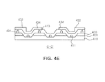
- FIGS. 4a to 4e are a schematic perspective view, a plan view, and a sectional view showing a semiconductor light emitting device according to another exemplary embodiment of the present invention. Specifically, FIGS. 4c, 4d , and 4e are sectional views taken along lines A-A', B-B', and C-C' in FIG. 4b .
- the semiconductor light emitting device includes a first conductive semiconductor layer 410 including first and second areas alternately disposed and having a stripe shape, an active layer 420 disposed on the second area, a second conductive semiconductor layer 430 disposed on the active layer 420, first and second electrode branches 411 and 431, a first electrode pad electrically connected to the first electrode branch 411 and disposed to be separated from the first conductive semiconductor layer 410, a second electrode pad 432 electrically connected to the second electrode branch 431 and disposed to be separated from the second conductive semiconductor layer 430, and an insulating part 440 formed on the first and second conductive semiconductor layers 410 and 430.
- At least one first conductive via 413 electrically connected to the first electrode branch 411 and at least one second conductive via 433 electrically connected to the second electrode branch 431 may be penetratingly formed through portions of the insulating part 440 in a thicknesswise direction.
- the first and second electrode branches 411 and 431 are formed to be parallel to each other, have a linear shape, and are alternately disposed.
- a first connection part 414 extends from the first electrode pad 412 to the first conductive via 413 along the upper surface of the insulating part 440 and a second connection part 434 extends from the second electrode pad 432 to the second conductive via 433 along the upper surface of the insulating part 440.
- the plurality of first and second electrode branches 411 and 431 are alternately disposed.
- the respective elements and their connective relationships within the semiconductor light emitting device according to the present exemplary embodiment will now be described in detail with reference to the accompanying drawings.
- the first and second conductive semiconductor layers formed on the first and second area, respectively, may have a protrusion and depression structure having a stripe shape in which protrusions and depresses are alternately repeated.
- the first and second electrode branches 411 and 431 are electrically connected to the first and second conductive semiconductor layers 410 and 430, and may be alternately disposed to have a stripe shape.
- the interval between the first and second electrode branches 411 and 431 can be uniform, and according to an embodiment, a larger number of first and second electrode branches 411 and 431 may be disposed so that the interval between the first and second electrode branches 411 and 431 becomes narrower. Accordingly, when current is applied through the electrode branches, a current flow in the interior of the first and second conductive semiconductor layers 410 and 430 electrically connected to the electrode branches can uniformly spread in the area between the first and second electrode branches 411 and 431, rather than being concentrated in one area.
- a plurality of first conductive vias 413 may be formed at an area of the insulating part 440 such that they are electrically connected to the first electrode branches 411 through the insulating part 440 (i.e., in a penetrative manner) in a thicknesswise direction
- a plurality of one second conductive via 433 may be formed at an area of the insulating part 440 such that they are electrically connected to the second electrode branches 431 through the insulating part 440 (i.e., in a penetrative manner) in a thicknesswise direction.
- the upper surface of the insulating part 440 has a rectangular shape, and the first and second conductive vias 413 and 433 may be disposed to be adjacent to one side and the other side opposed to the one side, respectively, when viewed from above. Namely, as shown in FIG. 4b , the first and second conductive vias 413 and 433 may be formed in a lengthwise direction along the respective sides. Accordingly, the first and second conductive vias 413 and 433 can be separated as far as possible from each other and accordingly, the current spreading effect can be improved.
- first and second conductive vias 413 and 433 can be electrically connected to the first connection part 414 extending from the first electrode pad 412 to the first conductive via 413 along the upper surface of the insulating part 440 and a second connection part 434 extending from the second electrode pad 432 to the second conductive via 433 along the upper surface of the insulating part 440, respectively.
- first and second connection parts 414 and 434 extend along the formation direction so as to be electrically connected to the first and second conductive vias 413 and 433.
- the first and second pads 412 and 432 can be electrically connected through the first and second through the first and second connection parts 414 and 434, without having to be provided to every first and second electrode branches 411 and 431.
- the first and second pads 412 and 432 may not be limitedly disposed on the first and second branch electrodes 411 and 431; namely, the first and second pads 412 and 432 may be variably selectively disposed on any area of the upper surface of the insulating part 440 according to embodiments.
- first electrode pad and one second electrode pad may be formed or a plurality of first and second electrode pads may be formed according to embodiments.
- one first electrode pad 412 and two second electrode pads 432 are illustrated to be disposed.
- the first and second electrode pads 412 and 432 are formed to be adjacent to the sides opposed on the upper surface of the insulating part 440 having a rectangular shape and, in particular, the first electrode pad 412 is positioned at an area spaced apart by the same distance from the two second electrode pads 432, the current can spread more effectively.
- light extraction efficiency can be improved by implementing excellent current spreading.
Landscapes
- Led Devices (AREA)
Applications Claiming Priority (1)
| Application Number | Priority Date | Filing Date | Title |
|---|---|---|---|
| KR1020100107809A KR20120045919A (ko) | 2010-11-01 | 2010-11-01 | 반도체 발광소자 |
Publications (3)
| Publication Number | Publication Date |
|---|---|
| EP2448014A2 true EP2448014A2 (de) | 2012-05-02 |
| EP2448014A3 EP2448014A3 (de) | 2015-04-22 |
| EP2448014B1 EP2448014B1 (de) | 2020-01-01 |
Family
ID=44582608
Family Applications (1)
| Application Number | Title | Priority Date | Filing Date |
|---|---|---|---|
| EP11180652.7A Active EP2448014B1 (de) | 2010-11-01 | 2011-09-09 | Lichtemittierendes Halbleiterbauelement |
Country Status (5)
| Country | Link |
|---|---|
| US (2) | US8581293B2 (de) |
| EP (1) | EP2448014B1 (de) |
| KR (1) | KR20120045919A (de) |
| CN (1) | CN102468390B (de) |
| TW (1) | TWI459594B (de) |
Families Citing this family (8)
| Publication number | Priority date | Publication date | Assignee | Title |
|---|---|---|---|---|
| US7952646B2 (en) * | 2006-12-27 | 2011-05-31 | Intel Corporation | Method and apparatus for content adaptive spatial-temporal motion adaptive noise reduction |
| TWI446578B (zh) * | 2010-09-23 | 2014-07-21 | Epistar Corp | 發光元件及其製法 |
| CN103489980A (zh) * | 2012-06-12 | 2014-01-01 | 群康科技(深圳)有限公司 | 一种发光元件及其制作方法 |
| CN104425538B (zh) * | 2013-09-03 | 2019-05-03 | 晶元光电股份有限公司 | 具有多个发光结构的发光元件 |
| TWI509835B (zh) * | 2013-10-01 | 2015-11-21 | Opto Tech Corp | 白光二極體 |
| KR102410809B1 (ko) * | 2017-08-25 | 2022-06-20 | 쑤저우 레킨 세미컨덕터 컴퍼니 리미티드 | 반도체 소자 |
| CN113036014B (zh) * | 2019-12-25 | 2022-07-05 | 深圳第三代半导体研究院 | 一种垂直集成单元发光二极管 |
| CN116469983A (zh) * | 2021-07-29 | 2023-07-21 | 厦门三安光电有限公司 | 一种led芯片 |
Citations (1)
| Publication number | Priority date | Publication date | Assignee | Title |
|---|---|---|---|---|
| KR20100107809A (ko) | 2009-03-26 | 2010-10-06 | 현대제철 주식회사 | 크롭 절단장치 |
Family Cites Families (15)
| Publication number | Priority date | Publication date | Assignee | Title |
|---|---|---|---|---|
| EP0622858B2 (de) | 1993-04-28 | 2004-09-29 | Nichia Corporation | Halbleitervorrichtung aus einer galliumnitridartigen III-V-Halbleiterverbindung und Verfahren zu ihrer Herstellung |
| US6307218B1 (en) * | 1998-11-20 | 2001-10-23 | Lumileds Lighting, U.S., Llc | Electrode structures for light emitting devices |
| US6614056B1 (en) | 1999-12-01 | 2003-09-02 | Cree Lighting Company | Scalable led with improved current spreading structures |
| ATE448589T1 (de) * | 2001-04-12 | 2009-11-15 | Nichia Corp | Halbleiterelement aus galliumnitridzusammensetzung |
| EP1398839B1 (de) * | 2001-04-23 | 2012-03-28 | Panasonic Corporation | Lichtemittierende einrichtung mit einem leuchtdioden-chip |
| US7179670B2 (en) * | 2004-03-05 | 2007-02-20 | Gelcore, Llc | Flip-chip light emitting diode device without sub-mount |
| US7615798B2 (en) * | 2004-03-29 | 2009-11-10 | Nichia Corporation | Semiconductor light emitting device having an electrode made of a conductive oxide |
| US7285801B2 (en) * | 2004-04-02 | 2007-10-23 | Lumination, Llc | LED with series-connected monolithically integrated mesas |
| WO2006043422A1 (ja) * | 2004-10-19 | 2006-04-27 | Nichia Corporation | 半導体素子 |
| JP2007173269A (ja) * | 2005-12-19 | 2007-07-05 | Showa Denko Kk | フリップチップ型半導体発光素子、フリップチップ型半導体発光素子の製造方法、フリップチップ型半導体発光素子の実装構造及び発光ダイオードランプ |
| US8022419B2 (en) * | 2005-12-19 | 2011-09-20 | Showa Denko K.K. | Flip-chip type semiconductor light-emitting device, method for manufacturing flip-chip type semiconductor light-emitting device, printed circuit board for flip-chip type semiconductor light-emitting device, mounting structure for flip-chip type semiconductor light-emitting device, and light-emitting diode lamp |
| US7842963B2 (en) | 2006-10-18 | 2010-11-30 | Koninklijke Philips Electronics N.V. | Electrical contacts for a semiconductor light emitting apparatus |
| CN102779918B (zh) * | 2007-02-01 | 2015-09-02 | 日亚化学工业株式会社 | 半导体发光元件 |
| JP2009295611A (ja) * | 2008-06-02 | 2009-12-17 | Sharp Corp | 半導体発光素子及びその製造方法 |
| JP5057398B2 (ja) | 2008-08-05 | 2012-10-24 | シャープ株式会社 | 窒化物半導体発光素子およびその製造方法 |
-
2010
- 2010-11-01 KR KR1020100107809A patent/KR20120045919A/ko not_active Ceased
-
2011
- 2011-09-01 US US13/223,877 patent/US8581293B2/en active Active
- 2011-09-09 EP EP11180652.7A patent/EP2448014B1/de active Active
- 2011-09-20 TW TW100133713A patent/TWI459594B/zh active
- 2011-09-21 CN CN201110282791.8A patent/CN102468390B/zh active Active
-
2013
- 2013-11-08 US US14/075,519 patent/US8928027B2/en active Active
Patent Citations (1)
| Publication number | Priority date | Publication date | Assignee | Title |
|---|---|---|---|---|
| KR20100107809A (ko) | 2009-03-26 | 2010-10-06 | 현대제철 주식회사 | 크롭 절단장치 |
Also Published As
| Publication number | Publication date |
|---|---|
| EP2448014B1 (de) | 2020-01-01 |
| US8581293B2 (en) | 2013-11-12 |
| EP2448014A3 (de) | 2015-04-22 |
| TW201220536A (en) | 2012-05-16 |
| US20120104449A1 (en) | 2012-05-03 |
| US20140061713A1 (en) | 2014-03-06 |
| CN102468390A (zh) | 2012-05-23 |
| US8928027B2 (en) | 2015-01-06 |
| TWI459594B (zh) | 2014-11-01 |
| KR20120045919A (ko) | 2012-05-09 |
| CN102468390B (zh) | 2016-04-27 |
Similar Documents
| Publication | Publication Date | Title |
|---|---|---|
| US8928027B2 (en) | Semiconductor light emitting device | |
| CN102983129B (zh) | 发光器件 | |
| CN104025296B (zh) | 光电子半导体芯片 | |
| CN102456799B (zh) | 半导体发光器件及其制造方法 | |
| US8785962B2 (en) | Semiconductor light emitting device having current blocking layer | |
| US20120228580A1 (en) | Light-emitting diode device and method for manufacturing the same | |
| US8450765B2 (en) | Light emitting diode chip and method for manufacturing the same | |
| JP6714328B2 (ja) | 発光素子及び照明システム | |
| US10784427B2 (en) | Light-emitting diode device | |
| US10937938B2 (en) | Light emitting device | |
| JP2007311781A (ja) | 窒化物系半導体発光ダイオード | |
| US20120037946A1 (en) | Light emitting devices | |
| EP3652792B1 (de) | Lichtemittierende diode und herstellungsverfahren davon | |
| CN112397626A (zh) | 一种发光二极管 | |
| US20180198022A1 (en) | Semiconductor light emitting device including floating conductive pattern | |
| US9178110B2 (en) | Light-emitting device and method for manufacturing same | |
| US20140091351A1 (en) | Light emitting diode chip | |
| KR20120016830A (ko) | 반도체 발광 소자 및 발광 장치 | |
| US20140131759A1 (en) | Semiconductor light-emitting element | |
| KR20130101299A (ko) | 반도체 발광소자 및 그 제조 방법 | |
| KR20170083519A (ko) | 반도체 발광소자 | |
| KR20160093789A (ko) | 반도체 발광소자 | |
| KR100747641B1 (ko) | 발광 다이오드 | |
| KR100801618B1 (ko) | 발광 소자 및 그 제조방법 | |
| KR20110086982A (ko) | 반도체 발광소자 및 이를 제조하는 방법 |
Legal Events
| Date | Code | Title | Description |
|---|---|---|---|
| PUAI | Public reference made under article 153(3) epc to a published international application that has entered the european phase |
Free format text: ORIGINAL CODE: 0009012 |
|
| 17P | Request for examination filed |
Effective date: 20110909 |
|
| AK | Designated contracting states |
Kind code of ref document: A2 Designated state(s): AL AT BE BG CH CY CZ DE DK EE ES FI FR GB GR HR HU IE IS IT LI LT LU LV MC MK MT NL NO PL PT RO RS SE SI SK SM TR |
|
| AX | Request for extension of the european patent |
Extension state: BA ME |
|
| RAP1 | Party data changed (applicant data changed or rights of an application transferred) |
Owner name: SAMSUNG ELECTRONICS CO., LTD. |
|
| PUAL | Search report despatched |
Free format text: ORIGINAL CODE: 0009013 |
|
| AK | Designated contracting states |
Kind code of ref document: A3 Designated state(s): AL AT BE BG CH CY CZ DE DK EE ES FI FR GB GR HR HU IE IS IT LI LT LU LV MC MK MT NL NO PL PT RO RS SE SI SK SM TR |
|
| AX | Request for extension of the european patent |
Extension state: BA ME |
|
| RIC1 | Information provided on ipc code assigned before grant |
Ipc: H01L 33/20 20100101ALN20150313BHEP Ipc: H01L 33/42 20100101ALN20150313BHEP Ipc: H01L 27/15 20060101ALI20150313BHEP Ipc: H01L 33/62 20100101ALN20150313BHEP Ipc: H01L 33/38 20100101AFI20150313BHEP Ipc: H01L 33/44 20100101ALI20150313BHEP |
|
| STAA | Information on the status of an ep patent application or granted ep patent |
Free format text: STATUS: EXAMINATION IS IN PROGRESS |
|
| 17Q | First examination report despatched |
Effective date: 20190321 |
|
| GRAP | Despatch of communication of intention to grant a patent |
Free format text: ORIGINAL CODE: EPIDOSNIGR1 |
|
| STAA | Information on the status of an ep patent application or granted ep patent |
Free format text: STATUS: GRANT OF PATENT IS INTENDED |
|
| RIC1 | Information provided on ipc code assigned before grant |
Ipc: H01L 33/42 20100101ALN20190801BHEP Ipc: H01L 27/15 20060101ALI20190801BHEP Ipc: H01L 33/38 20100101AFI20190801BHEP Ipc: H01L 33/20 20100101ALN20190801BHEP Ipc: H01L 33/44 20100101ALI20190801BHEP Ipc: H01L 33/62 20100101ALI20190801BHEP |
|
| RIC1 | Information provided on ipc code assigned before grant |
Ipc: H01L 33/20 20100101ALN20190806BHEP Ipc: H01L 33/38 20100101AFI20190806BHEP Ipc: H01L 33/62 20100101ALI20190806BHEP Ipc: H01L 27/15 20060101ALI20190806BHEP Ipc: H01L 33/44 20100101ALI20190806BHEP Ipc: H01L 33/42 20100101ALN20190806BHEP |
|
| INTG | Intention to grant announced |
Effective date: 20190821 |
|
| GRAS | Grant fee paid |
Free format text: ORIGINAL CODE: EPIDOSNIGR3 |
|
| GRAA | (expected) grant |
Free format text: ORIGINAL CODE: 0009210 |
|
| STAA | Information on the status of an ep patent application or granted ep patent |
Free format text: STATUS: THE PATENT HAS BEEN GRANTED |
|
| AK | Designated contracting states |
Kind code of ref document: B1 Designated state(s): AL AT BE BG CH CY CZ DE DK EE ES FI FR GB GR HR HU IE IS IT LI LT LU LV MC MK MT NL NO PL PT RO RS SE SI SK SM TR |
|
| REG | Reference to a national code |
Ref country code: GB Ref legal event code: FG4D |
|
| REG | Reference to a national code |
Ref country code: CH Ref legal event code: EP Ref country code: AT Ref legal event code: REF Ref document number: 1220896 Country of ref document: AT Kind code of ref document: T Effective date: 20200115 |
|
| REG | Reference to a national code |
Ref country code: DE Ref legal event code: R096 Ref document number: 602011064328 Country of ref document: DE |
|
| REG | Reference to a national code |
Ref country code: IE Ref legal event code: FG4D |
|
| REG | Reference to a national code |
Ref country code: NL Ref legal event code: MP Effective date: 20200101 |
|
| REG | Reference to a national code |
Ref country code: LT Ref legal event code: MG4D |
|
| PG25 | Lapsed in a contracting state [announced via postgrant information from national office to epo] |
Ref country code: NL Free format text: LAPSE BECAUSE OF FAILURE TO SUBMIT A TRANSLATION OF THE DESCRIPTION OR TO PAY THE FEE WITHIN THE PRESCRIBED TIME-LIMIT Effective date: 20200101 Ref country code: LT Free format text: LAPSE BECAUSE OF FAILURE TO SUBMIT A TRANSLATION OF THE DESCRIPTION OR TO PAY THE FEE WITHIN THE PRESCRIBED TIME-LIMIT Effective date: 20200101 Ref country code: CZ Free format text: LAPSE BECAUSE OF FAILURE TO SUBMIT A TRANSLATION OF THE DESCRIPTION OR TO PAY THE FEE WITHIN THE PRESCRIBED TIME-LIMIT Effective date: 20200101 Ref country code: PT Free format text: LAPSE BECAUSE OF FAILURE TO SUBMIT A TRANSLATION OF THE DESCRIPTION OR TO PAY THE FEE WITHIN THE PRESCRIBED TIME-LIMIT Effective date: 20200527 Ref country code: NO Free format text: LAPSE BECAUSE OF FAILURE TO SUBMIT A TRANSLATION OF THE DESCRIPTION OR TO PAY THE FEE WITHIN THE PRESCRIBED TIME-LIMIT Effective date: 20200401 Ref country code: FI Free format text: LAPSE BECAUSE OF FAILURE TO SUBMIT A TRANSLATION OF THE DESCRIPTION OR TO PAY THE FEE WITHIN THE PRESCRIBED TIME-LIMIT Effective date: 20200101 Ref country code: RS Free format text: LAPSE BECAUSE OF FAILURE TO SUBMIT A TRANSLATION OF THE DESCRIPTION OR TO PAY THE FEE WITHIN THE PRESCRIBED TIME-LIMIT Effective date: 20200101 |
|
| PG25 | Lapsed in a contracting state [announced via postgrant information from national office to epo] |
Ref country code: SE Free format text: LAPSE BECAUSE OF FAILURE TO SUBMIT A TRANSLATION OF THE DESCRIPTION OR TO PAY THE FEE WITHIN THE PRESCRIBED TIME-LIMIT Effective date: 20200101 Ref country code: LV Free format text: LAPSE BECAUSE OF FAILURE TO SUBMIT A TRANSLATION OF THE DESCRIPTION OR TO PAY THE FEE WITHIN THE PRESCRIBED TIME-LIMIT Effective date: 20200101 Ref country code: HR Free format text: LAPSE BECAUSE OF FAILURE TO SUBMIT A TRANSLATION OF THE DESCRIPTION OR TO PAY THE FEE WITHIN THE PRESCRIBED TIME-LIMIT Effective date: 20200101 Ref country code: GR Free format text: LAPSE BECAUSE OF FAILURE TO SUBMIT A TRANSLATION OF THE DESCRIPTION OR TO PAY THE FEE WITHIN THE PRESCRIBED TIME-LIMIT Effective date: 20200402 Ref country code: IS Free format text: LAPSE BECAUSE OF FAILURE TO SUBMIT A TRANSLATION OF THE DESCRIPTION OR TO PAY THE FEE WITHIN THE PRESCRIBED TIME-LIMIT Effective date: 20200501 Ref country code: BG Free format text: LAPSE BECAUSE OF FAILURE TO SUBMIT A TRANSLATION OF THE DESCRIPTION OR TO PAY THE FEE WITHIN THE PRESCRIBED TIME-LIMIT Effective date: 20200401 |
|
| REG | Reference to a national code |
Ref country code: DE Ref legal event code: R097 Ref document number: 602011064328 Country of ref document: DE |
|
| PG25 | Lapsed in a contracting state [announced via postgrant information from national office to epo] |
Ref country code: SM Free format text: LAPSE BECAUSE OF FAILURE TO SUBMIT A TRANSLATION OF THE DESCRIPTION OR TO PAY THE FEE WITHIN THE PRESCRIBED TIME-LIMIT Effective date: 20200101 Ref country code: EE Free format text: LAPSE BECAUSE OF FAILURE TO SUBMIT A TRANSLATION OF THE DESCRIPTION OR TO PAY THE FEE WITHIN THE PRESCRIBED TIME-LIMIT Effective date: 20200101 Ref country code: RO Free format text: LAPSE BECAUSE OF FAILURE TO SUBMIT A TRANSLATION OF THE DESCRIPTION OR TO PAY THE FEE WITHIN THE PRESCRIBED TIME-LIMIT Effective date: 20200101 Ref country code: ES Free format text: LAPSE BECAUSE OF FAILURE TO SUBMIT A TRANSLATION OF THE DESCRIPTION OR TO PAY THE FEE WITHIN THE PRESCRIBED TIME-LIMIT Effective date: 20200101 Ref country code: DK Free format text: LAPSE BECAUSE OF FAILURE TO SUBMIT A TRANSLATION OF THE DESCRIPTION OR TO PAY THE FEE WITHIN THE PRESCRIBED TIME-LIMIT Effective date: 20200101 Ref country code: SK Free format text: LAPSE BECAUSE OF FAILURE TO SUBMIT A TRANSLATION OF THE DESCRIPTION OR TO PAY THE FEE WITHIN THE PRESCRIBED TIME-LIMIT Effective date: 20200101 |
|
| PLBE | No opposition filed within time limit |
Free format text: ORIGINAL CODE: 0009261 |
|
| STAA | Information on the status of an ep patent application or granted ep patent |
Free format text: STATUS: NO OPPOSITION FILED WITHIN TIME LIMIT |
|
| REG | Reference to a national code |
Ref country code: AT Ref legal event code: MK05 Ref document number: 1220896 Country of ref document: AT Kind code of ref document: T Effective date: 20200101 |
|
| 26N | No opposition filed |
Effective date: 20201002 |
|
| PG25 | Lapsed in a contracting state [announced via postgrant information from national office to epo] |
Ref country code: AT Free format text: LAPSE BECAUSE OF FAILURE TO SUBMIT A TRANSLATION OF THE DESCRIPTION OR TO PAY THE FEE WITHIN THE PRESCRIBED TIME-LIMIT Effective date: 20200101 Ref country code: IT Free format text: LAPSE BECAUSE OF FAILURE TO SUBMIT A TRANSLATION OF THE DESCRIPTION OR TO PAY THE FEE WITHIN THE PRESCRIBED TIME-LIMIT Effective date: 20200101 |
|
| PG25 | Lapsed in a contracting state [announced via postgrant information from national office to epo] |
Ref country code: PL Free format text: LAPSE BECAUSE OF FAILURE TO SUBMIT A TRANSLATION OF THE DESCRIPTION OR TO PAY THE FEE WITHIN THE PRESCRIBED TIME-LIMIT Effective date: 20200101 Ref country code: SI Free format text: LAPSE BECAUSE OF FAILURE TO SUBMIT A TRANSLATION OF THE DESCRIPTION OR TO PAY THE FEE WITHIN THE PRESCRIBED TIME-LIMIT Effective date: 20200101 |
|
| PG25 | Lapsed in a contracting state [announced via postgrant information from national office to epo] |
Ref country code: MC Free format text: LAPSE BECAUSE OF FAILURE TO SUBMIT A TRANSLATION OF THE DESCRIPTION OR TO PAY THE FEE WITHIN THE PRESCRIBED TIME-LIMIT Effective date: 20200101 |
|
| REG | Reference to a national code |
Ref country code: CH Ref legal event code: PL |
|
| REG | Reference to a national code |
Ref country code: BE Ref legal event code: MM Effective date: 20200930 |
|
| PG25 | Lapsed in a contracting state [announced via postgrant information from national office to epo] |
Ref country code: LU Free format text: LAPSE BECAUSE OF NON-PAYMENT OF DUE FEES Effective date: 20200909 |
|
| PG25 | Lapsed in a contracting state [announced via postgrant information from national office to epo] |
Ref country code: FR Free format text: LAPSE BECAUSE OF NON-PAYMENT OF DUE FEES Effective date: 20200930 |
|
| PG25 | Lapsed in a contracting state [announced via postgrant information from national office to epo] |
Ref country code: IE Free format text: LAPSE BECAUSE OF NON-PAYMENT OF DUE FEES Effective date: 20200909 Ref country code: LI Free format text: LAPSE BECAUSE OF NON-PAYMENT OF DUE FEES Effective date: 20200930 Ref country code: BE Free format text: LAPSE BECAUSE OF NON-PAYMENT OF DUE FEES Effective date: 20200930 Ref country code: CH Free format text: LAPSE BECAUSE OF NON-PAYMENT OF DUE FEES Effective date: 20200930 |
|
| PG25 | Lapsed in a contracting state [announced via postgrant information from national office to epo] |
Ref country code: TR Free format text: LAPSE BECAUSE OF FAILURE TO SUBMIT A TRANSLATION OF THE DESCRIPTION OR TO PAY THE FEE WITHIN THE PRESCRIBED TIME-LIMIT Effective date: 20200101 Ref country code: MT Free format text: LAPSE BECAUSE OF FAILURE TO SUBMIT A TRANSLATION OF THE DESCRIPTION OR TO PAY THE FEE WITHIN THE PRESCRIBED TIME-LIMIT Effective date: 20200101 Ref country code: CY Free format text: LAPSE BECAUSE OF FAILURE TO SUBMIT A TRANSLATION OF THE DESCRIPTION OR TO PAY THE FEE WITHIN THE PRESCRIBED TIME-LIMIT Effective date: 20200101 |
|
| PG25 | Lapsed in a contracting state [announced via postgrant information from national office to epo] |
Ref country code: MK Free format text: LAPSE BECAUSE OF FAILURE TO SUBMIT A TRANSLATION OF THE DESCRIPTION OR TO PAY THE FEE WITHIN THE PRESCRIBED TIME-LIMIT Effective date: 20200101 Ref country code: AL Free format text: LAPSE BECAUSE OF FAILURE TO SUBMIT A TRANSLATION OF THE DESCRIPTION OR TO PAY THE FEE WITHIN THE PRESCRIBED TIME-LIMIT Effective date: 20200101 |
|
| P01 | Opt-out of the competence of the unified patent court (upc) registered |
Effective date: 20230520 |
|
| REG | Reference to a national code |
Ref country code: DE Ref legal event code: R079 Ref document number: 602011064328 Country of ref document: DE Free format text: PREVIOUS MAIN CLASS: H01L0033380000 Ipc: H10H0020831000 |
|
| PGFP | Annual fee paid to national office [announced via postgrant information from national office to epo] |
Ref country code: DE Payment date: 20250722 Year of fee payment: 15 |
|
| PGFP | Annual fee paid to national office [announced via postgrant information from national office to epo] |
Ref country code: GB Payment date: 20250724 Year of fee payment: 15 |