EP2442364A1 - Gate stack structure for semiconductor flash memory device and preparation method thereof - Google Patents
Gate stack structure for semiconductor flash memory device and preparation method thereof Download PDFInfo
- Publication number
- EP2442364A1 EP2442364A1 EP11789049A EP11789049A EP2442364A1 EP 2442364 A1 EP2442364 A1 EP 2442364A1 EP 11789049 A EP11789049 A EP 11789049A EP 11789049 A EP11789049 A EP 11789049A EP 2442364 A1 EP2442364 A1 EP 2442364A1
- Authority
- EP
- European Patent Office
- Prior art keywords
- film
- layer
- nanocrystals
- ald
- stack structure
- Prior art date
- Legal status (The legal status is an assumption and is not a legal conclusion. Google has not performed a legal analysis and makes no representation as to the accuracy of the status listed.)
- Withdrawn
Links
Images


Classifications
-
- C—CHEMISTRY; METALLURGY
- C23—COATING METALLIC MATERIAL; COATING MATERIAL WITH METALLIC MATERIAL; CHEMICAL SURFACE TREATMENT; DIFFUSION TREATMENT OF METALLIC MATERIAL; COATING BY VACUUM EVAPORATION, BY SPUTTERING, BY ION IMPLANTATION OR BY CHEMICAL VAPOUR DEPOSITION, IN GENERAL; INHIBITING CORROSION OF METALLIC MATERIAL OR INCRUSTATION IN GENERAL
- C23C—COATING METALLIC MATERIAL; COATING MATERIAL WITH METALLIC MATERIAL; SURFACE TREATMENT OF METALLIC MATERIAL BY DIFFUSION INTO THE SURFACE, BY CHEMICAL CONVERSION OR SUBSTITUTION; COATING BY VACUUM EVAPORATION, BY SPUTTERING, BY ION IMPLANTATION OR BY CHEMICAL VAPOUR DEPOSITION, IN GENERAL
- C23C16/00—Chemical coating by decomposition of gaseous compounds, without leaving reaction products of surface material in the coating, i.e. chemical vapour deposition [CVD] processes
- C23C16/44—Chemical coating by decomposition of gaseous compounds, without leaving reaction products of surface material in the coating, i.e. chemical vapour deposition [CVD] processes characterised by the method of coating
- C23C16/455—Chemical coating by decomposition of gaseous compounds, without leaving reaction products of surface material in the coating, i.e. chemical vapour deposition [CVD] processes characterised by the method of coating characterised by the method used for introducing gases into reaction chamber or for modifying gas flows in reaction chamber
- C23C16/45523—Pulsed gas flow or change of composition over time
- C23C16/45525—Atomic layer deposition [ALD]
-
- B—PERFORMING OPERATIONS; TRANSPORTING
- B82—NANOTECHNOLOGY
- B82Y—SPECIFIC USES OR APPLICATIONS OF NANOSTRUCTURES; MEASUREMENT OR ANALYSIS OF NANOSTRUCTURES; MANUFACTURE OR TREATMENT OF NANOSTRUCTURES
- B82Y10/00—Nanotechnology for information processing, storage or transmission, e.g. quantum computing or single electron logic
-
- C—CHEMISTRY; METALLURGY
- C23—COATING METALLIC MATERIAL; COATING MATERIAL WITH METALLIC MATERIAL; CHEMICAL SURFACE TREATMENT; DIFFUSION TREATMENT OF METALLIC MATERIAL; COATING BY VACUUM EVAPORATION, BY SPUTTERING, BY ION IMPLANTATION OR BY CHEMICAL VAPOUR DEPOSITION, IN GENERAL; INHIBITING CORROSION OF METALLIC MATERIAL OR INCRUSTATION IN GENERAL
- C23C—COATING METALLIC MATERIAL; COATING MATERIAL WITH METALLIC MATERIAL; SURFACE TREATMENT OF METALLIC MATERIAL BY DIFFUSION INTO THE SURFACE, BY CHEMICAL CONVERSION OR SUBSTITUTION; COATING BY VACUUM EVAPORATION, BY SPUTTERING, BY ION IMPLANTATION OR BY CHEMICAL VAPOUR DEPOSITION, IN GENERAL
- C23C16/00—Chemical coating by decomposition of gaseous compounds, without leaving reaction products of surface material in the coating, i.e. chemical vapour deposition [CVD] processes
- C23C16/22—Chemical coating by decomposition of gaseous compounds, without leaving reaction products of surface material in the coating, i.e. chemical vapour deposition [CVD] processes characterised by the deposition of inorganic material, other than metallic material
- C23C16/30—Deposition of compounds, mixtures or solid solutions, e.g. borides, carbides, nitrides
- C23C16/40—Oxides
-
- H—ELECTRICITY
- H10—SEMICONDUCTOR DEVICES; ELECTRIC SOLID-STATE DEVICES NOT OTHERWISE PROVIDED FOR
- H10D—INORGANIC ELECTRIC SEMICONDUCTOR DEVICES
- H10D30/00—Field-effect transistors [FET]
- H10D30/60—Insulated-gate field-effect transistors [IGFET]
- H10D30/68—Floating-gate IGFETs
- H10D30/6891—Floating-gate IGFETs characterised by the shapes, relative sizes or dispositions of the floating gate electrode
- H10D30/6893—Floating-gate IGFETs characterised by the shapes, relative sizes or dispositions of the floating gate electrode wherein the floating gate has multiple non-connected parts, e.g. multi-particle floating gate
-
- H—ELECTRICITY
- H10—SEMICONDUCTOR DEVICES; ELECTRIC SOLID-STATE DEVICES NOT OTHERWISE PROVIDED FOR
- H10D—INORGANIC ELECTRIC SEMICONDUCTOR DEVICES
- H10D30/00—Field-effect transistors [FET]
- H10D30/60—Insulated-gate field-effect transistors [IGFET]
- H10D30/69—IGFETs having charge trapping gate insulators, e.g. MNOS transistors
- H10D30/694—IGFETs having charge trapping gate insulators, e.g. MNOS transistors characterised by the shapes, relative sizes or dispositions of the gate electrodes
-
- H—ELECTRICITY
- H10—SEMICONDUCTOR DEVICES; ELECTRIC SOLID-STATE DEVICES NOT OTHERWISE PROVIDED FOR
- H10D—INORGANIC ELECTRIC SEMICONDUCTOR DEVICES
- H10D64/00—Electrodes of devices having potential barriers
- H10D64/01—Manufacture or treatment
- H10D64/013—Manufacture or treatment of electrodes having a conductor capacitively coupled to a semiconductor by an insulator
- H10D64/01302—Manufacture or treatment of electrodes having a conductor capacitively coupled to a semiconductor by an insulator the insulator being formed after the semiconductor body, the semiconductor being silicon
- H10D64/01304—Manufacture or treatment of electrodes having a conductor capacitively coupled to a semiconductor by an insulator the insulator being formed after the semiconductor body, the semiconductor being silicon characterised by the conductor
- H10D64/01316—Manufacture or treatment of electrodes having a conductor capacitively coupled to a semiconductor by an insulator the insulator being formed after the semiconductor body, the semiconductor being silicon characterised by the conductor the conductor comprising a layer of elemental metal contacting the insulator, e.g. Ta, W, Mo or Al
-
- H—ELECTRICITY
- H10—SEMICONDUCTOR DEVICES; ELECTRIC SOLID-STATE DEVICES NOT OTHERWISE PROVIDED FOR
- H10D—INORGANIC ELECTRIC SEMICONDUCTOR DEVICES
- H10D64/00—Electrodes of devices having potential barriers
- H10D64/01—Manufacture or treatment
- H10D64/031—Manufacture or treatment of data-storage electrodes
- H10D64/035—Manufacture or treatment of data-storage electrodes comprising conductor-insulator-conductor-insulator-semiconductor structures
-
- H—ELECTRICITY
- H10—SEMICONDUCTOR DEVICES; ELECTRIC SOLID-STATE DEVICES NOT OTHERWISE PROVIDED FOR
- H10D—INORGANIC ELECTRIC SEMICONDUCTOR DEVICES
- H10D64/00—Electrodes of devices having potential barriers
- H10D64/01—Manufacture or treatment
- H10D64/031—Manufacture or treatment of data-storage electrodes
- H10D64/037—Manufacture or treatment of data-storage electrodes comprising charge-trapping insulators
-
- H—ELECTRICITY
- H10—SEMICONDUCTOR DEVICES; ELECTRIC SOLID-STATE DEVICES NOT OTHERWISE PROVIDED FOR
- H10D—INORGANIC ELECTRIC SEMICONDUCTOR DEVICES
- H10D64/00—Electrodes of devices having potential barriers
- H10D64/60—Electrodes characterised by their materials
- H10D64/66—Electrodes having a conductor capacitively coupled to a semiconductor by an insulator, e.g. MIS electrodes
- H10D64/665—Electrodes having a conductor capacitively coupled to a semiconductor by an insulator, e.g. MIS electrodes the conductor comprising a layer of elemental metal contacting the insulator, e.g. tungsten or molybdenum
Definitions
- the present invention relates to the fabrication of semiconductor integrated circuits, and, particularly to an electric capacity structure and a fabricating method of a flash memory capacitor. More specifically, it relates to a gate stack structure and a fabricating method with a novel heterogenous charge storage layer composed of metal nanocrystals and high permittivity (high-k) dielectric .
- nonvolatile memory based on discrete-charge storage nodes (such as nanocrystal memory and SONOS-type memory etc) has drawn great attention.
- the aforementioned memory devices use discrete charge traps to store charges in place of continuous poly-silicon floating gate, which can prevent a loss of massive charges stored in the charge-trapping layer through local defects in the tunnel layer, thus efficiently enhancing the data retention of memory, and achieving lower operating voltage and higher programming/erasing speed.
- metal nanocrystals Compared with semiconductor nanocrystals, metal nanocrystals have some advantages such as higher density of states around Fermi level, a wider range of work functions, stronger coupling with substrate channel and so on. Accordingly, the above mentioned advantages can ensure that the memory device has lower operating voltage, higher stored charge density and longer charge retention. Some research indicates that a deep potential well can be formed by using high work-function metal nanocrystals, thus efficiently trapping charges and offering better data retention.
- the object of the present invention is to provide a gate stack structure for use in a semiconductor flash memory device, which has a high stored-charge density, a low operating voltage, fast programing and erasing speeds, as well as good charge retention.
- the other object of the present invention is to offer a method of fabricating the above-mentioned gate stack structure.
- the present invention provides a gate stack structure for use in a semiconductor flash memory device and its fabricating method.
- the said gate stack structure contains a heterogeneous charge storage layer based on metal nanocrystals and high-k film.
- the aforementioned gate stack structure includes the following components in sequence from bottom to up:
- the above-mentioned high-k film can be HfAlO, as an example, it may consist of HfO 2 and Al 2 O 3 with a deposition cycle ratio of 1:1; Alternatively, said high-k film can be an HfO 2 film.
- the aforementioned top electrode layer contains a gate electrode which is composed of metal palladium (Pd).
- the fabricating method of the aforementioned gate stack structure includes the following steps:
- the high-k Hf x Al y O z film described in Step 3.2 can be HfAlO, which consists of HfO 2 and Al 2 O 3 with a deposition cycle ratio of 1:1.
- the said high-k Hf x Al y O z film can be HfO 2 .
- the experimental conditions for ALD (atomic layer deposition) of HfO 2 film are as follows: the substrate temperature is kept at 250 ⁇ 350°C, and the reaction precursors include tetrakis(ethylmethylamino)-hafnium (TEMAH) and water vapor.
- TEMAH tetrakis(ethylmethylamino)-hafnium
- step 3.2 and Step 4 the experimental conditions for ALD of Al 2 O 3 film are as follows: the substrate temperature is kept at 250 ⁇ 350°C, and the reaction precursors include trimethylaluminium (TMA) and water vapor.
- TMA trimethylaluminium
- the annealing temperature for the formation of RuO x nanocrystals is 700 ⁇ 900°C, and the annealing time is 10-30s.
- said rapid thermal annealing is carried out at 500 ⁇ 800°C for 10-30s during the formation of the Al 2 O 3 charge blocking layer.
- the gate electrode material is a metal of Pd.
- the aforementioned fabricating method also includes:
- the gate stack structure provided by the present invention will be very promising for next generation flash memory devices.
- the present invention relates to a gate stack structure for use in a semiconductor flash memory device, in particular, the related gate stack structure contains a heterogeneous charge storage layer consisting of metal nanocrystals and high-k film.
- Said flash memory capacitor includes the following components in sequence from bottom to top:
- Hf x Al y O z film is composed of HfO 2 and Al 2 O 3 with a deposition cycle ratio of 1:1, denoted by HfAlO.
- HfAlO a deposition cycle ratio of 1:1
- the temperature of the substrate is kept at a range of 250 ⁇ 350°C, and the precursors for HfO 2 include Tetrakis (ethylmethylamino) Hafnium (TEMAH) and water vapor.
- TEMAH Tetrakis (ethylmethylamino) Hafnium
- Al 2 O3 is as described in Step 2.
- HfAlO or HfO 2 film is controlled in a range of 3 ⁇ 20 nm (preferred thickness is 5 ⁇ 10 nm). Based on the difference of Hf x Al y O z film thickness, it is found that the Hf x Al y O z film can be present between nanocrystals when it is thin, but it cannot completely fill the gap between the nanocrystals. Otherwise, it can fill the gap between the nanocrystals completely when it is thick, as shown in Fig. 1 .
- Fig. 2 shows the flat-band voltages resulting from programming and erasing of the fabricated memory capacitors with different heterogeneous charge storage layer under different voltages for 0.1ms, respectively, .
- the programming voltage positive bias
- the resulting flat-band voltage shifts gradually towards a positive bias, and this is due to negative charge trapping caused by electron injection.
- the erasing voltage negative bias
- the resulting flat-band voltage moves gradually in the direction of negative bias, which is attributed to de-trapping of the negative charges stored in the charge storage layer or injection of holes from the substrate.
- the heterogeneous charge storage layer of RuO x /HfO 2 can provide a larger memory window than RuO x /HfAlO in the case of identical operating voltages.
- the former can result in a memory window of 2.6V, and the latter can lead to a memory window of 1.4V in the case of a 6V operating voltage.
- FIG. 3 shows the resulting flat-band voltages after programming under +9V and erasing under -9V of the fabricated memory capacitors with different heterogeneous charge storage layer for different times. It is seen that the resulting flat-band voltage increases with time under programming and erasing modes and finally tends to saturation. Regarding 0.1ms programming/erasing time, a memory window of around 2V was achieved for the RuO x /HfAlO charge storage layer-based capacitor, and a memory window of 3.5V was obtained for the RuO x /HfO 2 charge storage layer-based capacitor. Therefore, both of the capacitors exhibit fast programming and erasing characteristics under low operating voltages.
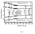
- Fig. 4 shows the retention characteristics of the fabricated memory capacitors with the heterogeneous charge storage layer-based gate stack structure after programming at +9V for 1ms and erasing at -9V for 1ms, respectively.
- the resulting memory window is close to 3.4V after ten years by extrapolation, thus exhibiting excellent charge retention.
- the charge trapping dielectric of HfAlO the corresponding memory window is around 1.6V.
- the present invention combines the advantages of both metal nanocrystals and high-k dielectrics, which act as the heterogeneous charge storage layer in the gate stack structure.
- the utilization of this kind of heterogeneous charge storage layer containing high-k dielectrics enhances the electric field across the charge tunnel layer, thus leading to a decrease in the potential barrier for charge injection, an increase in programming and erasing speeds and achievement of low operating voltages.
- the metal nanocrystals with a high work function can result in the formation of a deeper potential well, which can ensure good charge retention after charges trapping.
- the metal nanocrystals in the present invention are composed of Ru and Ru oxide (denoted by RuO x nanocrystals), which have excellent thermal stability. Though Ru is oxidized, it is still a good conductor. In addition, it does not diffuse easily at high temperature, and it is easy for dry etching.
- the top electrode of Pd in the present invention has a high work function of 5.22eV, and thus it combines with the charge blocking layer, resulting in a potential barrier propitious to programming and erasing.
- Pd has good chemical and thermal stabilities.
- the gate stack structure provided by the present invention will be very promising for next generation flash memory devices.
Landscapes
- Chemical & Material Sciences (AREA)
- Engineering & Computer Science (AREA)
- Nanotechnology (AREA)
- General Chemical & Material Sciences (AREA)
- Chemical Kinetics & Catalysis (AREA)
- Materials Engineering (AREA)
- Mechanical Engineering (AREA)
- Metallurgy (AREA)
- Organic Chemistry (AREA)
- Inorganic Chemistry (AREA)
- Mathematical Physics (AREA)
- Theoretical Computer Science (AREA)
- Crystallography & Structural Chemistry (AREA)
- Physics & Mathematics (AREA)
- Semiconductor Memories (AREA)
- Non-Volatile Memory (AREA)
Abstract
Description
- The present invention relates to the fabrication of semiconductor integrated circuits, and, particularly to an electric capacity structure and a fabricating method of a flash memory capacitor. More specifically, it relates to a gate stack structure and a fabricating method with a novel heterogenous charge storage layer composed of metal nanocrystals and high permittivity (high-k) dielectric .
- With development of semiconductor process and technology, the integration density of nonvolatile flash memory becomes higher and higher, at the same time, the operating voltage becomes lower and lower. Therefore, these drive a continuous shrinkage of memory device. Beyond 65nm technology node, the conventional poly-silicon floating gate memory device will face many problems, thus the memory device performance will be affected, such as low programming/erasing speed, high operating voltage etc.
- Recently, a new type of nonvolatile memory based on discrete-charge storage nodes (such as nanocrystal memory and SONOS-type memory etc) has drawn great attention. The aforementioned memory devices use discrete charge traps to store charges in place of continuous poly-silicon floating gate, which can prevent a loss of massive charges stored in the charge-trapping layer through local defects in the tunnel layer, thus efficiently enhancing the data retention of memory, and achieving lower operating voltage and higher programming/erasing speed.
- Compared with semiconductor nanocrystals, metal nanocrystals have some advantages such as higher density of states around Fermi level, a wider range of work functions, stronger coupling with substrate channel and so on. Accordingly, the above mentioned advantages can ensure that the memory device has lower operating voltage, higher stored charge density and longer charge retention. Some research indicates that a deep potential well can be formed by using high work-function metal nanocrystals, thus efficiently trapping charges and offering better data retention.
- On the other hand, with the development of the SONOS-type memories, it has been proposed that high-k materials are employed to replace the charge trapping layer of silicon nitride in the SONOS-type memory, which can enhance the electric field across the tunnel layer. This further increases programming and erasing speeds. However, relatively high operating voltages and slow operating speed are the major drawbacks of the SONOS-type memory.
- The object of the present invention is to provide a gate stack structure for use in a semiconductor flash memory device, which has a high stored-charge density, a low operating voltage, fast programing and erasing speeds, as well as good charge retention. The other object of the present invention is to offer a method of fabricating the above-mentioned gate stack structure.
- To achieve the above-mentioned objects, the present invention provides a gate stack structure for use in a semiconductor flash memory device and its fabricating method. Herein, the said gate stack structure contains a heterogeneous charge storage layer based on metal nanocrystals and high-k film. The aforementioned gate stack structure includes the following components in sequence from bottom to up:
- A p-type (100) monocrystalline silicon wafer used as a substrate;
- an Al2O3 film with a thickness of 5∼15nm formed by ALD (atomic layer deposition) which serves as a charge tunnel layer;
- said heterogeneous charge storage layer further includes the following:
- said metal nanocrystals acting as a first charge trapping layer, which is a composite consisting of Ru and Ru oxide, denoted as RuOx nanocrystals;
- said ALD high-k film with a thickness of 3∼20nm acting as a second charge trapping layer, said high-k dielectric is HfxAlyOz, where x>0, z>0 and y=0 or y>0;
- an Al2O3 film with a thickness of 15∼40nm formed by ALD, which serves as a charge blocking layer; and
- a top electrode layer.
- The above-mentioned high-k film can be HfAlO, as an example, it may consist of HfO2 and Al2O3 with a deposition cycle ratio of 1:1; Alternatively, said high-k film can be an HfO2 film.
- The aforementioned top electrode layer contains a gate electrode which is composed of metal palladium (Pd).
- The fabricating method of the aforementioned gate stack structure includes the following steps:
-
Step 1, providing a p-type (100) monocrystalline silicon wafer as a substrate. -
Step 2, growing an Al2O3 film with a thickness of 5∼15nm on the Si substrate by ALD (atomic layer deposition), which acts as a tunnel layer. - Step 3.1, depositing a 2∼4 nm Ru thin film on the Al2O3 tunnel layer using a magnetron sputtering technique, followed by rapid thermal annealing (RTA) in nitrogen environment, thus forming RuOx nanocrystals, which serve as the first charge trapping layer in the heterogeneous charge storage layer, the aforementioned RuOx nanocrystals being a composite of metal Ru and Ru oxide.
- Step 3.2, growing a high-k HfxAlyOz thin film with a thickness of 3∼20nm by ALD, which is used as the second charge-trapping layer in the heterogeneous charge storage layer, wherein for the aforementioned high-k HfxAlyOz film, , x>0, , y=0 or y>0. Herein, the atomic contents of Hf and Al can be determined by deposition cycles of HfO2 and Al2O3;
-
Step 4, growing a 15∼40nm film of Al2O3 by ALD, which acts as a charge blocking layer, followed by rapid thermal annealing; - Step 5, forming a gate electrode with a thickness of 50∼200 nm by lithography and lift-off process, which serves as the top electrode layer.
- The high-k HfxAlyOz film described in Step 3.2 can be HfAlO, which consists of HfO2 and Al2O3 with a deposition cycle ratio of 1:1. Alternatively, the said high-k HfxAlyOz film can be HfO2 .
- As described in step 3.2, the experimental conditions for ALD (atomic layer deposition) of HfO2 film are as follows: the substrate temperature is kept at 250∼350°C, and the reaction precursors include tetrakis(ethylmethylamino)-hafnium (TEMAH) and water vapor.
- As described in
step 2, step 3.2 andStep 4, the experimental conditions for ALD of Al2O3 film are as follows: the substrate temperature is kept at 250∼350°C, and the reaction precursors include trimethylaluminium (TMA) and water vapor. - As described in Step 3.1, the annealing temperature for the formation of RuOx nanocrystals is 700∼900°C, and the annealing time is 10-30s. In
step 4, said rapid thermal annealing is carried out at 500∼800°C for 10-30s during the formation of the Al2O3 charge blocking layer. - In Step 5, the gate electrode material is a metal of Pd.
- The aforementioned fabricating method also includes:
-
Step 6, removing the native oxide on the back side of silicon substrate using diluted HF solution, and then depositing an Al layer as a bottom electrode in order to form a good ohmic contact. - The gate stack structure for use in a semiconductor flash memory device of the present invention and its fabricating method have the following advantages as follows:
- 1. Depositing ultra-thin metallic Ru films using magnetic sputtering technique allows. the thickness and deposition rate of the film to be controlled precisely by optimizing sputtering power, deposition time and substrate temperature etc in high vacuum, thereby forming ultra-thin and uniform metal films. This makes it easier to form small dimensional, uniformly distributed and high density nanocrystals.
- 2. The RuOx nanocrystals are used to form the first charge trapping layer as the charge storage center, which can achieve a large depth of potential well due to a high work function of 4.7-5.2eVThis helps to improve the charge storage capability. In the present invention, the formation temperature of the RuOx nanocrystals is compatible with the process temperature of the memory devices, which does not exceed the annealing temperature for source and drain activation after ion implantation during device fabrication.
- 3. The high-k HfxAlyOz material is introduced as the second charge trapping layer, which can effectively enhance the electric field across the tunnel layer due to its high dielectric constant of 10∼25. This will increase the programming and erasing speeds of the memory device, and reduce the operating voltage. Furthermore, the HfxAlyOz material can offer enough charge traps for charge storage.
- 4. The heterogeneous charge storage layer composed of high-k HfxAlyOz and high density RuOx nanocrystals can jointly trap charges injected from the substrate. This greatly increases the density of the stored charges. Moreover, the combination of high density RuOx nanocrystals with HfxAlyOz film effectively restrains crystallization of HfxAAlyOz dielectric after high temperature annealing, thus reducing charge leakage along grain boundaries and enhancing charge retention of the memory device.
- 5. ALD is used to deposit the HfxAlyOz film. This can not only control the composition and thickness of the film accurately, but also effectively fill a nano-scale gap. Therefore, the RuOx nanocrystals can be isolated completely by HfxAlyOz dielectric.
- 6. Pd is used as an electrode, which can, together with the blocking Al2O3 layer, form a barrier helpful to programming and erasing. It also ensures good chemical and thermal stabilities due to immunity to oxidation. Furthermore, Pd film is deposited on the Al2O3 film by electron beam evaporation in a high vacuum, thereby resulting in good contact between Pd and Al2O3. This can improve the performance of the memory capacitor.
- Accordingly, the gate stack structure provided by the present invention will be very promising for next generation flash memory devices.
-
-
FIG. 1 shows a cross-sectional view of the gate stack structure of memory capacitor with a heterogeneous charge storage layer of RuOx nanocrystals and high-k HfxAlyOz film. -
Fig. 2 shows flat-band voltages resulting from programming and erasing of the fabricated memory capacitors with different heterogeneous charge storage layer under different voltages for 0.1ms. -
FIG. 3 shows the resulting flat-band voltages after programming under +9V and erasing under -9V of the fabricated memory capacitors with different heterogeneous charge storage layer for different times.. -
FIG. 4 shows the charge retention characteristics of the fabricated memory capacitors with different heterogeneous charge storage layer after programming at +9V and erasing at -9V for 1ms, respectively. - Referring to
FIG. 1 , the present invention relates to a gate stack structure for use in a semiconductor flash memory device, in particular, the related gate stack structure contains a heterogeneous charge storage layer consisting of metal nanocrystals and high-k film. Said flash memory capacitor includes the following components in sequence from bottom to top: - (1) A p-type monocrystalline silicon wafer with orientation 100 used as a substrate;
- (2) An Al2O3 film with a thickness of 5∼15nm grown on the silicon substrate by atomic layer deposition, which acts as a tunnel layer;
- (3) Said heterogeneous charge storage layer further includes:
- metal nanocrytsals acting as a first charge trapping layer, which is consisting of Ru and Ru oxide (denoted by RuOx nanocyrstals);
- a high-k film with a thickness of 3∼20 nm (preferred thickness is 5∼10nm) grown by ALD acting as a second charge trapping layer, the dielectric of said high-k is HfxAlyOz, (x>0, z>0 and y=0 or y>0); the dielectric constant being 10∼25.
- (4) An Al2O3 film with a thickness of 15∼40nm film grown by ALD, which acts as a charge blocking layer.
- (5) A top electrode layer containing a gate electrode made of metal Pd. The above-mentioned gate stack structure for use in a semiconductor flash memory device contains a heterogeneous charge storage layer, which can be fabricated as follows:
-
Step 1, providing A p-type 100 silicon wafer with a resistivity of 8∼12 Ω.cm as a substrate. Firstly, the silicon wafer is cleaned with a standard method, and the residual native oxide is removed by diluted HF solution. -
Step 2, growing a charge tunnel layer of Al2O3 by ALD using the precursors of trimethylaluminium and H2O at 250∼350°C. The thickness of the Al2O3 layer is controlled in a range of 5∼15nm. - Step 3.1, forming the RuOx nanocrystals of the heterogeneous charge storage layer: an ultra-thin Ru film with a thickness of 2∼4nm is deposited on the Al2O3 tunnel layer by magnetic sputtering, followed by rapid thermal annealing in N2 environment at 700∼900°C for 10∼30s. The resulting RuOx nanocrystals are used as the first charge trapping layer.
- Step 3.2, forming a high-k HfxAlyOz film of the heterogeneous charge storage layer by ALD, which is used as the second charge trapping layer.
-
- One form of said HfxAlyOz film is composed of HfO2 and Al2O3 with a deposition cycle ratio of 1:1, denoted by HfAlO. Another form of said HfxAlyOz film is a pure HfO2 film without incorporation of Al2O3.
- As for the above-mentioned two forms of HfxAlyOz film, the temperature of the substrate is kept at a range of 250∼350°C, and the precursors for HfO2 include Tetrakis (ethylmethylamino) Hafnium (TEMAH) and water vapor. The formation of Al2O3 is as described in
Step 2. - The thickness of HfAlO or HfO2 film is controlled in a range of 3∼20 nm (preferred thickness is 5∼10 nm). Based on the difference of HfxAlyOz film thickness, it is found that the HfxAlyOz film can be present between nanocrystals when it is thin, but it cannot completely fill the gap between the nanocrystals. Otherwise, it can fill the gap between the nanocrystals completely when it is thick, as shown in
Fig. 1 . -
Step 4. forming the charge blocking layer of Al2O3: firstly, a 15∼40nm film of Al2O3 is grown by ALD, which acts as a charge blocking layer, the conditions for the ALD are as follows: the substrate temperature is kept at 250∼350°C, and the precursors include trimethylaluminium and water vapor. And then the resulting sample is treated by rapid thermal annealing in N2 environment at 500∼800°C for 10∼30s. This aims to acquire high quality Al2O3 blocking layer to restrain charges leaking. - Step 5. forming a top electrode by a lift-off technique. That is, the electrode pattern is firstly formed by lithography, and then a Pd film with a thickness of 50-200nm is deposited by electron beam evaporation. Finally, the remaining photoresist is removed by acetone.
-
Step 6. For electrical measurements of the device, the native oxide on the back of the silicon substrate is removed by diluted HF solution, and then a layer of Al is deposited on it, which serves as a bottom electrode to ensure a good ohmic contact. Hereto, the fabricating process of the aforementioned gate stack structure with a heterogeneous charge storage layer is completed. -
Fig. 2 shows the flat-band voltages resulting from programming and erasing of the fabricated memory capacitors with different heterogeneous charge storage layer under different voltages for 0.1ms, respectively, . As the programming voltage (positive bias) increases, the resulting flat-band voltage shifts gradually towards a positive bias, and this is due to negative charge trapping caused by electron injection. As the erasing voltage (negative bias) increases, the resulting flat-band voltage moves gradually in the direction of negative bias, which is attributed to de-trapping of the negative charges stored in the charge storage layer or injection of holes from the substrate. Furthermore, it is observed that the heterogeneous charge storage layer of RuOx/HfO2 can provide a larger memory window than RuOx/HfAlO in the case of identical operating voltages. As an example, the former can result in a memory window of 2.6V, and the latter can lead to a memory window of 1.4V in the case of a 6V operating voltage. -
FIG. 3 shows the resulting flat-band voltages after programming under +9V and erasing under -9V of the fabricated memory capacitors with different heterogeneous charge storage layer for different times. It is seen that the resulting flat-band voltage increases with time under programming and erasing modes and finally tends to saturation. Regarding 0.1ms programming/erasing time, a memory window of around 2V was achieved for the RuOx/HfAlO charge storage layer-based capacitor, and a memory window of 3.5V was obtained for the RuOx/HfO2 charge storage layer-based capacitor. Therefore, both of the capacitors exhibit fast programming and erasing characteristics under low operating voltages. -
Fig. 4 shows the retention characteristics of the fabricated memory capacitors with the heterogeneous charge storage layer-based gate stack structure after programming at +9V for 1ms and erasing at -9V for 1ms, respectively. In terms of the charge trapping dielectric of HfO2, the resulting memory window is close to 3.4V after ten years by extrapolation, thus exhibiting excellent charge retention. As for the charge trapping dielectric of HfAlO, the corresponding memory window is around 1.6V. - The aforementioned results indicate that the memory capacitors based on the heterogeneous charge storage layer of RuOx and HfxAlyOz exhibit fast programming and erasing characteristics under low voltages as well as excellent charge retention.
- To sum up, the present invention combines the advantages of both metal nanocrystals and high-k dielectrics, which act as the heterogeneous charge storage layer in the gate stack structure. The utilization of this kind of heterogeneous charge storage layer containing high-k dielectrics enhances the electric field across the charge tunnel layer, thus leading to a decrease in the potential barrier for charge injection, an increase in programming and erasing speeds and achievement of low operating voltages. Meanwhile, the metal nanocrystals with a high work function can result in the formation of a deeper potential well, which can ensure good charge retention after charges trapping.
- The metal nanocrystals in the present invention are composed of Ru and Ru oxide (denoted by RuOx nanocrystals), which have excellent thermal stability. Though Ru is oxidized, it is still a good conductor. In addition, it does not diffuse easily at high temperature, and it is easy for dry etching.
- The high-k dielectrics of HfxAlyOz (y=0 or y>0) in the present invention have a dielectric constant of 10∼25 and high density of charge traps. These enable HfxAlyOz to act as an ideal charge trapping layer instead of silicon nitride.
- The top electrode of Pd in the present invention has a high work function of 5.22eV, and thus it combines with the charge blocking layer, resulting in a potential barrier propitious to programming and erasing. In addition, Pd has good chemical and thermal stabilities.
- As a result, the gate stack structure provided by the present invention will be very promising for next generation flash memory devices.
- Although the invention has been described with respect to specific embodiments for a complete and clear disclosure, the appended claims are not to be thus limited but are to be construed as embodying all modifications and alternative constructions that may occur to one skilled in the art that fairly fall within the basic teaching herein set forth. Therefore, the protection scope of the present invention should be determined by the attached claims.
Claims (10)
- A gate stack structure for use in a semiconductor flash memory device comprising a heterogeneous charge storage layer based on metal nanocrystals and a high-k film; said gate stack structure comprising the following components in sequence from bottom to top,
a p-type monocrystalline silicon wafer with orientation 100 used as a substrate;
an Al2O3 film having a thickness of 5∼15nm grown on the silicon substrate by atomic layer deposition (ALD), which acts as a tunnel layer;
wherein said heterogeneous charge storage layer further includes:said metal nanocrystals acting as a first charge trapping layer, which is a composite consisting of Ru and Ru oxide, denoted by RuOx nanocrystals;said high-k film with a thickness of 3∼20nm grown by ALD acting as a second charge trapping layer, the dielectric of said high-k is HfxAlyOz, where x>0, z>0 and y=0 or y>0;an Al2O3 film with a thickness of 15∼40nm film grown by ALD, which acts as a charge blocking layer; anda top electrode layer. - The gate stack structure for use according to claim 1, wherein said high-k film is a film of HfAlO consisting of HfO2 and Al2O3 with a deposition cycle ratio of 1:1, or said high-k film is a pure HfO2 film.
- The gate stack structure for use according to claim 1, wherein said top electrode contains a gate electrode of metal Pd.
- A method of producing a gate stack structure for use in a semiconductor flash memory device comprising the following steps:step 1, providing a p-type monocrystalline silicon wafer with orientation 100 as a substrate;step 2, growing an Al2O3 film with a thickness of 5∼15nm on the silicon substrate by ALD, which acts as a tunnel layer;step 3.1, depositing a Ru film with a thickness of 2∼4nm on the Al2O3 tunnel layer by magnetic sputtering, followed by rapid thermal annealing in N2 environment, thus forming RuOx nanocrystals, said resulting RuOx nanocrystals serving as the first charge trapping layer in the heterogeneous charge storage layer, wherein said RuOx nanocrystals are a composite consisting of Ru and Ru oxide;step 3.2, growing a high-k HfxAlyOz film with a thickness of 3∼20nm by ALD, said high-k HfxAlyOz acting as the second charge trapping layer in the heterogeneous charge storage layer, wherein for the said high-k HfxAlyOz film, x>0, z>0,and, y=0 or y>0, and wherein the atomic compositions of Hf and Al are determined by deposition cycles of HfO2 and Al2O3;step 4, growing a 15∼40nm film of Al2O3 by ALD, which acts as a charge blocking layer, followed by rapid thermal annealing;step 5, forming a gate electrode with a thickness of 50∼200nm, which acts as the top electrode layer, by lithography and lift-off processes.
- The method of claim 4, wherein said high-k HfxAlyOz film described in step 3.2 is an HfAlO film, which is composed of HfO2 and Al2O3 with a deposition cycle ratio of 1:1; or, said high-k HfxAlyOz film is a pure HfO2 film.
- The method of claim 5, wherein the conditions for ALD of HfO2 film described in step 3.2 are as follows: the substrate temperature is kept at 250∼350°C, and the precursors of said deposition include Tetrakis (ethylmethylamino) Hafnium and water vapor.
- The method of claim 4 or 5 or 6, wherein, said conditions for ALD of Al2O3 film described in step 2, step 3.2 or step 4 are as follows: the substrate temperature is kept at 250∼350°C, and the precursors of said deposition include trimethylaluminium and water vapor.
- The method of claim 4, wherein, in step 3.1, the annealing temperature for the formation of RuOx nanocrystals is 700∼900°C, and the annealing time is 10-30s; in step 4, said rapid thermal annealing is carried out at 500∼800°C for 10∼30s.
- The method of claim 4, wherein, in step 5, the material of the gate electrode is metal Pd.
- The method of claim 4, further comprising:step 6, firstly removing the native oxide layer on the back of silicon wafer using diluted HF solution, and then depositing an Al layer as a bottom electrode in order to form a good ohmic contact.
Applications Claiming Priority (3)
| Application Number | Priority Date | Filing Date | Title |
|---|---|---|---|
| CN2010101916591A CN101887910A (en) | 2010-06-03 | 2010-06-03 | A gate stack structure suitable for semiconductor flash memory devices and its preparation method |
| CN2011101304848A CN102208442B (en) | 2010-06-03 | 2011-05-19 | Gate stack structure suitable for semiconductor flash memory device and manufacturing method of gate stack structure |
| PCT/CN2011/000891 WO2011150670A1 (en) | 2010-06-03 | 2011-05-24 | Gate stack structure for semiconductor flash memory device and preparation method thereof |
Publications (2)
| Publication Number | Publication Date |
|---|---|
| EP2442364A1 true EP2442364A1 (en) | 2012-04-18 |
| EP2442364A4 EP2442364A4 (en) | 2014-08-27 |
Family
ID=43073727
Family Applications (1)
| Application Number | Title | Priority Date | Filing Date |
|---|---|---|---|
| EP11789049.1A Withdrawn EP2442364A4 (en) | 2010-06-03 | 2011-05-24 | DOOR STACK STRUCTURE FOR SEMICONDUCTOR FLASH MEMORY DEVICE AND METHOD FOR PREPARING THE SAME |
Country Status (4)
| Country | Link |
|---|---|
| US (1) | US20130062684A1 (en) |
| EP (1) | EP2442364A4 (en) |
| CN (2) | CN101887910A (en) |
| WO (1) | WO2011150670A1 (en) |
Cited By (2)
| Publication number | Priority date | Publication date | Assignee | Title |
|---|---|---|---|---|
| WO2014113655A3 (en) * | 2013-01-18 | 2014-10-16 | The Trustees Of The University Of Pennsylvania | Nanocrystal thin film device fabrication methods and apparatus |
| US9336919B2 (en) | 2012-08-17 | 2016-05-10 | The Trustees Of The University Of Pennsylvania | Methods for preparing colloidal nanocrystal-based thin films |
Families Citing this family (14)
| Publication number | Priority date | Publication date | Assignee | Title |
|---|---|---|---|---|
| CN101887910A (en) * | 2010-06-03 | 2010-11-17 | 复旦大学 | A gate stack structure suitable for semiconductor flash memory devices and its preparation method |
| CN102646579B (en) * | 2011-02-17 | 2015-01-07 | 中芯国际集成电路制造(上海)有限公司 | Silicon oxide nitride oxide semiconductor (SONOS) structure and manufacturing method |
| CN102938404A (en) * | 2011-08-16 | 2013-02-20 | 北京天中磊智能科技有限公司 | Electrically erasable programmable read only memory (EEPROM) storage chip especial for intelligent ammeter |
| CN102623459B (en) * | 2012-04-10 | 2015-01-07 | 复旦大学 | Thin-film transistor memory and preparation method thereof |
| US10720504B2 (en) | 2015-09-11 | 2020-07-21 | Intel Corporation | Transistor with dynamic threshold voltage for low-leakage standby and high speed active mode |
| KR102331474B1 (en) | 2017-06-19 | 2021-11-29 | 삼성전자주식회사 | Semiconductor devices |
| JP2019062170A (en) | 2017-09-28 | 2019-04-18 | ルネサスエレクトロニクス株式会社 | Semiconductor device and method for manufacturing the same |
| CN108649031A (en) * | 2018-04-09 | 2018-10-12 | 复旦大学 | Ultrafast quasi- nonvolatile storage of two dimension based on self-rectifying elastomeric material and preparation method thereof |
| CN108588677B (en) * | 2018-04-18 | 2020-09-08 | 北京航空航天大学 | High-dielectric-constant nano laminated dielectric film and preparation method thereof |
| TWI815891B (en) * | 2018-06-21 | 2023-09-21 | 美商應用材料股份有限公司 | Thin films and methods of depositing thin films |
| CN109116691B (en) * | 2018-09-25 | 2022-08-16 | 湖南哲龙科技有限公司 | Formula for weakening influence of substrate surface on characteristics of organic photosensitive drum |
| CN112080732B (en) * | 2020-07-29 | 2021-12-28 | 西安交通大学 | Silicon integrated BT-BMZ film, capacitor and manufacturing method thereof |
| CN112908999A (en) * | 2021-03-25 | 2021-06-04 | 复旦大学 | Manufacturing process of semi-floating gate memory and semi-floating gate memory |
| US12356624B2 (en) * | 2021-08-30 | 2025-07-08 | Renesas Electronics Corporation | Semiconductor device and method of manufacturing the same |
Family Cites Families (7)
| Publication number | Priority date | Publication date | Assignee | Title |
|---|---|---|---|---|
| US7012297B2 (en) * | 2001-08-30 | 2006-03-14 | Micron Technology, Inc. | Scalable flash/NV structures and devices with extended endurance |
| KR100672998B1 (en) * | 2005-02-14 | 2007-01-24 | 삼성전자주식회사 | Nonvolatile Memory Device, Driving Method and Forming Method thereof |
| US7629641B2 (en) * | 2005-08-31 | 2009-12-08 | Micron Technology, Inc. | Band engineered nano-crystal non-volatile memory device utilizing enhanced gate injection |
| US7847341B2 (en) * | 2006-12-20 | 2010-12-07 | Nanosys, Inc. | Electron blocking layers for electronic devices |
| KR100900569B1 (en) * | 2007-03-29 | 2009-06-02 | 국민대학교산학협력단 | Floating gate forming method and manufacturing method of nonvolatile memory device using same |
| CN101692463B (en) * | 2009-09-24 | 2011-12-14 | 复旦大学 | Capacitor structure of mixed nano-crystal memory and preparation method thereof |
| CN101887910A (en) * | 2010-06-03 | 2010-11-17 | 复旦大学 | A gate stack structure suitable for semiconductor flash memory devices and its preparation method |
-
2010
- 2010-06-03 CN CN2010101916591A patent/CN101887910A/en active Pending
-
2011
- 2011-05-19 CN CN2011101304848A patent/CN102208442B/en not_active Expired - Fee Related
- 2011-05-24 WO PCT/CN2011/000891 patent/WO2011150670A1/en not_active Ceased
- 2011-05-24 EP EP11789049.1A patent/EP2442364A4/en not_active Withdrawn
- 2011-05-24 US US13/518,306 patent/US20130062684A1/en not_active Abandoned
Cited By (5)
| Publication number | Priority date | Publication date | Assignee | Title |
|---|---|---|---|---|
| US9336919B2 (en) | 2012-08-17 | 2016-05-10 | The Trustees Of The University Of Pennsylvania | Methods for preparing colloidal nanocrystal-based thin films |
| US10096733B2 (en) | 2012-08-17 | 2018-10-09 | The Trustees Of The University Of Pennsylvania | Methods for the preparation of colloidal nanocrystal dispersion |
| US10096734B2 (en) | 2012-08-17 | 2018-10-09 | The Trustees Of The University Of Pennsylvania | Methods of forming colloidal nanocrystal-based thin film devices |
| WO2014113655A3 (en) * | 2013-01-18 | 2014-10-16 | The Trustees Of The University Of Pennsylvania | Nanocrystal thin film device fabrication methods and apparatus |
| US9865465B2 (en) | 2013-01-18 | 2018-01-09 | The Trustees Of The University Of Pennsylvania | Nanocrystal thin film fabrication methods and apparatus |
Also Published As
| Publication number | Publication date |
|---|---|
| US20130062684A1 (en) | 2013-03-14 |
| EP2442364A4 (en) | 2014-08-27 |
| WO2011150670A1 (en) | 2011-12-08 |
| CN102208442B (en) | 2013-04-17 |
| CN101887910A (en) | 2010-11-17 |
| CN102208442A (en) | 2011-10-05 |
Similar Documents
| Publication | Publication Date | Title |
|---|---|---|
| EP2442364A1 (en) | Gate stack structure for semiconductor flash memory device and preparation method thereof | |
| US10211223B2 (en) | Vertical ferroelectric memory device and a method for manufacturing thereof | |
| US7183186B2 (en) | Atomic layer deposited ZrTiO4 films | |
| US20080023744A1 (en) | Nonvolatile semiconductor memory device and method of manufacturing the same | |
| KR20080031594A (en) | Charge trap type memory device | |
| US7579646B2 (en) | Flash memory with deep quantum well and high-K dielectric | |
| US20070120179A1 (en) | SONOS type non-volatile memory devices having a laminate blocking insulation layer and methods of manufacturing the same | |
| US7795159B2 (en) | Charge trap layer for a charge trap semiconductor memory device and method of manufacturing the same | |
| CN110911492A (en) | Electronic device and method of manufacturing the same | |
| JP2009135494A (en) | Nonvolatile memory device with improved immunity for erase saturation and method of manufacturing the same | |
| US7943984B2 (en) | Nonvolatile semiconductor memory apparatus | |
| US7635628B2 (en) | Nonvolatile memory device and method of manufacturing the same | |
| CN102231365B (en) | Preparation method of non-volatile charge storage device, non-volatile charge storage device and application of device | |
| CN102800632A (en) | A method of manufacturing a charge-trapping non-volatile memory | |
| US20070190721A1 (en) | Semiconductor memory device having an alloy metal gate electrode and method of manufacturing the same | |
| Wang et al. | Charge storage characteristics of Au nanocrystals embedded in high-k gate dielectrics on Si | |
| CN101673772A (en) | Erasable metal-insulator-silicon capacitor structure | |
| Zhu et al. | Design and Fabrication of Ta $ _ {2} $ O $ _ {5} $ Stacks for Discrete Multibit Memory Application | |
| Kim et al. | Reduction of charge-transport characteristics of SiGe dot floating gate memory device with ZrO/sub 2/tunneling oxide | |
| TWI836349B (en) | Thin-film storage transistor with ferroelectric storage layer | |
| US20160071948A1 (en) | Non-Volatile Memory Device and Method for Manufacturing Same | |
| CN103545316B (en) | Based on the New Charge trap type memorizer of band gap regulation and control, its preparation method and application | |
| US20240138147A1 (en) | Three-dimensional memory device wordlines with reduced blocking layer damage | |
| Kim et al. | Optimization of Zr concentration in HZO-based charge trap layers for enhanced flash memory performance | |
| Das et al. | Ruthenium oxide metal nanocrystal capacitors with high-κ dielectric tunneling barriers for nanoscale nonvolatile memory device applications |
Legal Events
| Date | Code | Title | Description |
|---|---|---|---|
| PUAI | Public reference made under article 153(3) epc to a published international application that has entered the european phase |
Free format text: ORIGINAL CODE: 0009012 |
|
| 17P | Request for examination filed |
Effective date: 20120110 |
|
| AK | Designated contracting states |
Kind code of ref document: A1 Designated state(s): AL AT BE BG CH CY CZ DE DK EE ES FI FR GB GR HR HU IE IS IT LI LT LU LV MC MK MT NL NO PL PT RO RS SE SI SK SM TR |
|
| DAX | Request for extension of the european patent (deleted) | ||
| A4 | Supplementary search report drawn up and despatched |
Effective date: 20140729 |
|
| RIC1 | Information provided on ipc code assigned before grant |
Ipc: H01L 29/66 20060101ALI20140723BHEP Ipc: C23C 16/40 20060101ALI20140723BHEP Ipc: H01L 21/285 20060101ALI20140723BHEP Ipc: H01L 29/792 20060101ALI20140723BHEP Ipc: H01L 29/423 20060101ALI20140723BHEP Ipc: B82Y 10/00 20110101ALI20140723BHEP Ipc: H01L 21/28 20060101ALI20140723BHEP Ipc: H01L 29/49 20060101AFI20140723BHEP Ipc: H01L 27/115 20060101ALI20140723BHEP Ipc: C23C 16/455 20060101ALI20140723BHEP |
|
| STAA | Information on the status of an ep patent application or granted ep patent |
Free format text: STATUS: THE APPLICATION HAS BEEN WITHDRAWN |
|
| 18W | Application withdrawn |
Effective date: 20141223 |