EP2439545A2 - Power semiconductor device current detector circuit and detection method - Google Patents
Power semiconductor device current detector circuit and detection method Download PDFInfo
- Publication number
- EP2439545A2 EP2439545A2 EP11184204A EP11184204A EP2439545A2 EP 2439545 A2 EP2439545 A2 EP 2439545A2 EP 11184204 A EP11184204 A EP 11184204A EP 11184204 A EP11184204 A EP 11184204A EP 2439545 A2 EP2439545 A2 EP 2439545A2
- Authority
- EP
- European Patent Office
- Prior art keywords
- current
- terminal
- current detector
- voltage source
- circuit
- Prior art date
- Legal status (The legal status is an assumption and is not a legal conclusion. Google has not performed a legal analysis and makes no representation as to the accuracy of the status listed.)
- Withdrawn
Links
Images







Classifications
-
- G—PHYSICS
- G01—MEASURING; TESTING
- G01R—MEASURING ELECTRIC VARIABLES; MEASURING MAGNETIC VARIABLES
- G01R19/00—Arrangements for measuring currents or voltages or for indicating presence or sign thereof
- G01R19/0092—Measuring current only
-
- G—PHYSICS
- G01—MEASURING; TESTING
- G01R—MEASURING ELECTRIC VARIABLES; MEASURING MAGNETIC VARIABLES
- G01R31/00—Arrangements for testing electric properties; Arrangements for locating electric faults; Arrangements for electrical testing characterised by what is being tested not provided for elsewhere
- G01R31/26—Testing of individual semiconductor devices
- G01R31/2607—Circuits therefor
-
- G—PHYSICS
- G01—MEASURING; TESTING
- G01R—MEASURING ELECTRIC VARIABLES; MEASURING MAGNETIC VARIABLES
- G01R31/00—Arrangements for testing electric properties; Arrangements for locating electric faults; Arrangements for electrical testing characterised by what is being tested not provided for elsewhere
- G01R31/40—Testing power supplies
- G01R31/42—AC power supplies
Definitions
- the present invention relates to a power semiconductor device current detector circuit and detection method, and in particular, relates to a current detector circuit and detection method that detect a current flowing through a power semiconductor device such as a diode, thyristor, transistor (bipolar transistor or metal oxide semiconductor field effect transistor (MOSFET)), or insulated gate bipolar transistor (IGBT).
- a power semiconductor device such as a diode, thyristor, transistor (bipolar transistor or metal oxide semiconductor field effect transistor (MOSFET)), or insulated gate bipolar transistor (IGBT).
- a power conversion device such as an inverter or direct current (DC) chopper circuit.
- an output current detection is necessary in order to control these power conversion circuits.
- two methods are widely employed in the output current detection, which are
- Fig. 9 is a diagram showing an example of a configuration of a heretofore known three-phase inverter device in which a DCCT is used.
- the DCCT also called a direct current current transformer
- the DCCT utilizes a ring-like core and a Hall element, which is a magnetic sensor, as shown in JP-A-2000-134955 ( Figs. 1 and 18) shown below.
- Wiring is passed through the core, and the current is detected by detecting magnetism generated when current is passed through the wiring.
- the DCCT 105 is installed on the output wiring, and the detected current value is input into a control circuit 102.
- Fig. 10 is a diagram showing an example of a configuration of a heretofore known three-phase inverter device in which a shunt resistor is used.
- a shunt resistor 106 is connected in the lower arm of the inverter 101 shown in Fig. 10 .
- the output current is detected by detecting a voltage drop of the shunt resistor 106 at this time in the control circuit 102.
- a current detector circuit in which the shunt resistor is used is shown in, for example, JP-A-2003-274667 ( Figs. 1 , 4 , and 7 ) shown below.
- Fig. 11 is a diagram showing an example of a configuration of a heretofore known chopper circuit in which a shunt resistor is used.
- the shunt resistor 106 is connected to a ground (GND) line, as shown in Fig. 11 , and the voltage drop of the resistor 106 is detected.
- the control circuit 102 can detect a current when there is a boost chopper action from a direct current power source 103 in the direction of an aluminum electrolytic capacitor 108, and a current when there is a step down chopper action from the aluminum electrolytic capacitor 108 in the direction of the direct current power source 103.
- the heretofore known current detection methods have the kinds of problem indicated below. That is, with the current detection method in which a DCCT is used shown in Fig. 9 , there are problems in that the price is generally high because the DCCT uses a Hall sensor and a core, and that the output characteristics of the DCCT change due to the ambient temperature. Also, there is a problem in that the size of the detector increases because a core is used, and this restricts the miniaturization of the power conversion device.
- a current detecting function called a “sensing function-equipped power semiconductor device”
- a current detecting function-equipped power semiconductor device which are power semiconductor devices.
- IGBTs or FWDs configuring an inverter device there are ones called “sense IGBTs” and “sense FWDs” equipped with a current detecting function.
- the function will be described with a “sense IGBT” as an example.
- an IGBT is configured of a few thousand to a few tens of thousands of cells of the same structure. One portion of these is utilized as current detecting cells. In this case, an IGBT formed from the current detecting portion of the cells is called a "sensing region", and an IGBT formed from the other cells a "main region”. Then, generally, it is often the case that a ratio Nm/Ns between a main region cell quantity Nm (Nm is an integer) and a sensing region cell quantity Ns (Ns is an integer) is set at a few thousand to one.
- emitter terminals are divided into a main emitter terminal (hereafter called a main terminal) and a current detecting emitter terminal (hereafter called a sense terminal).
- a main terminal hereafter called a main terminal
- a current detecting emitter terminal hereafter called a sense terminal.
- An IGBT with this kind of configuration is represented by the kind of symbolic circuit shown in Fig. 13A . Also, an equivalent circuit thereof is represented as in Fig. 13B .
- a free wheeling diode In the case of a free wheeling diode (FWD) too, one portion of the chip is divided off for current detecting in the same way, and anode terminals are divided into a main anode terminal (hereafter, a main terminal) and a current detecting anode terminal (hereafter, a sense terminal).
- a main anode terminal hereafter, a main terminal
- a current detecting anode terminal hereafter, a sense terminal
- IPM intelligent power module
- Im / Is Nm + Ns / Ns ⁇ Nm / Ns
- Im is the main current (the current flowing through the main IGBT)
- Is is the sense current (the current flowing through the sense IGBT)
- Nm is the main region cell quantity
- Ns is the sensing region cell quantity. Therefore, a shunt resistor Rs is connected to the sense terminal as in Fig. 12 , a sense current Is is detected, and the main current is calculated based on Equation 2 below.
- a a factor caused by differences in characteristics between the main region and sensing region. That the current ratio is proportional to the cell quantity ratio is based on the premise that the characteristics of each cell of the main region and sensing region are the same. However, as there is actually variation in the characteristics, the ratio between the main current and sense current is not constant. When illustrating this on a graph, the relationship between the main current and sense current is not linear (refer to the characteristics before correction in Fig. 14 ).
- the invention has an object of solving the three problems shown below. That is, 1. to reduce an increase in size and increase in loss of the current detector when using a direct current transformer (DCCT) or shunt resistor (for detecting the main current). 2. To ensure that no decrease in current detection accuracy occurs when utilizing a sensing function-equipped power semiconductor device (semiconductor device). 3. To achieve a digital control of a correction circuit that improves the current detection accuracy of the sensing function-equipped power semiconductor device (power semiconductor element), and a suppression of the circuit scale.
- DCCT direct current transformer
- shunt resistor for detecting the main current.
- the object is a: to realize a small current detector circuit with low loss by detecting current using the sensing function of a power semiconductor element.
- b In this case, to correct the linearity of the main current Im and sense current Is, and improve the current detection accuracy.
- c To enable a digital control of a correction circuit that corrects the linearity, with a realizable circuit scale.
- a configuration principle of a power semiconductor device current detector circuit of the invention taking the difference in characteristics between a main region and sensing region to be due to the difference between a threshold voltage and internal resistance of each IGBT, is that the current detector circuit is configured in such a way as to correct the difference between the threshold voltage and internal resistance of each IGBT.
- the invention relates to a current detector circuit for a semiconductor device including a power semiconductor element, wherein the power semiconductor element is divided into a main region and a sensing region (current detecting region), including a terminal (main terminal) connected to the main region and a terminal (sense terminal) connected to the sensing region, the current detector circuit being connectable to the sense terminal.
- the current detector circuit comprises a current detector unit including a terminal into which a current to be detected is input, a terminal that has an input current as an output, and a terminal that outputs detected current information, and a variable voltage source circuit including a control input terminal for controlling an output voltage, and is configured in such a way that the current detector unit and variable voltage source circuit are connected in series, the current information output terminal of the current detector unit is connected to the control input of the variable voltage source circuit, and the current detector unit and variable voltage source circuit connected in series are connectable to the sense terminal and main terminal.
- the potential of the sense terminal is regulated by regulating the output voltage of the variable voltage source circuit in accordance with the current flowing through the sense terminal, thus correcting a difference in characteristics between the main region and sensing region.
- variable voltage source circuit comprises a variable resistor and a second variable voltage source circuit.
- the variable resistor, current detector unit, and the second variable voltage source circuit are connected in series, wherein the potential of the sense terminal is regulated by regulating the resistance value of the variable resistor and the output of the second variable voltage source circuit based on an output of the current information output terminal of the current detecting unit, thus correcting a difference in characteristics between the main region and sensing region.
- the current detector circuit is configured in such a way that an already known current is caused to flow through the main region, the current is detected from a sense terminal, and a gain and offset are regulated in order to correct the difference in characteristics between the main region and sensing region in accordance with the detected current. More specifically, the current detector circuit is configured in such a way that an already known current is caused to flow through the main region of the semiconductor device, the current is detected by a current detector unit connected to a sense terminal of the semiconductor device, a deviation in characteristics between the main region and sensing region is detected based on the detected current, and an offset amount and gain amount in an output regulator are regulated in such a way that the characteristics of the two coincide.
- the current detector circuit is configured in such a way that a parameter Kg that corrects a difference in internal resistance, and a parameter Ko that corrects a difference in internal threshold voltage, are set as correction parameters for improving the current detection accuracy of the semiconductor device, and the parameters can be changed from the exterior by a digital signal passing through a serial or parallel signal supply unit.
- an inverter device or chopper circuit configured to include an IGBT and FWD in upper arm and lower arm switching elements is configured in such a way that the IGBT provided in the upper arm is a sensing function-equipped IGBT and the FWD provided in the lower arm is a sensing function-equipped FWD, and the heretofore described current detector circuit is connected to the sense terminals of the sensing function-equipped IGBT and sensing function-equipped FWD.
- the invention it is possible to correct the sense characteristics of a power semiconductor element, and a highly accurate main current calculation is possible utilizing the sensing function.
- the main current detection is carried out using the sensing function in this way, it is possible to realize a miniaturization and decrease in loss of the current detector when compared with the heretofore known methods using a direct current current transformer (DCCT) or shunt resistor (for detecting the main current).
- DCCT direct current current transformer
- shunt resistor for detecting the main current
- the setting of the correction parameters can be carried out from the exterior using a serial or parallel signal supply unit, it is possible to realize an application circuit in which the current detector circuit of the invention is mounted in an appropriate circuit scale.
- the current detector circuit of the invention in the lower arm of an inverter device or the lower arm of a chopper circuit, it is possible to accurately detect the output current of the inverter device or chopper circuit.
- a configuration principle of a semiconductor device and a current detector circuit of the invention taking the difference in characteristics between a main region and sensing region to be due to the difference between a threshold voltage and internal resistance of each IGBT, is that the current detector circuit is configured in such a way as to correct the difference between the threshold voltage and internal resistance of each IGBT.
- the current detector circuit is configured in such a way that an already known current is caused to flow through the main region, the current is detected from a sense terminal, and a gain and offset are regulated in order to correct the difference in characteristics between the main region and sensing region in accordance with the detected current.
- the current detector circuit is configured in such a way that an already known current is caused to flow through the main region of the semiconductor device, the current is detected by a current detector unit connected to a sense terminal of the semiconductor device, a deviation in characteristics between the main region and sensing region is detected based on the detected current, and an offset amount and gain amount in an output regulator are regulated in such a way that the characteristics of the two coincide. A detailed description of this will be given hereafter. By so doing, it is possible to realize a small current detector circuit with low loss.
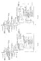
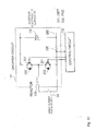
- Figs. 1A and 1B are diagrams showing a first configuration principle of the semiconductor device and the current detector circuit according to the embodiment of the invention.
- a current detector circuit 2 according to the embodiment of the invention is configured of a current detection unit 21 and a variable voltage source circuit 22. Then, the current detection unit 21 and variable voltage source circuit 22 are connected in series. Also, the current detector circuit 2 is connected between a sense terminal S and a main terminal M of a power semiconductor element 1 shown in an upper portion of Fig. 1A (the power semiconductor element 1 and the current detector circuit 2 forming together a semiconductor device).
- the configuration of the power semiconductor element 1 shown in the upper portion of Fig. 1A is basically the same as that shown in Figs. 13A and 13B .
- a current sensing output which is current information detected by the current detection unit 21, is input into an output regulator 221 that regulates the output voltage of the variable voltage source circuit 22.
- a gain Kg and offset Ko are set by the output regulator 221 in such a way that the output voltage of the variable voltage source circuit 22 is changed in accordance with the current detected by the current detection unit 21.
- Kg is set as a parameter correcting a difference in internal resistance
- Ko as a parameter correcting a difference in internal threshold voltage.
- the gain Kg and offset Ko function as a simulated resistance and offset voltage respectively, it is possible to correct a difference in characteristics between the main region and sensing region by regulating so that Rm ⁇ 0 ⁇ Rs ⁇ 0 + Kg Vthm ⁇ 0 ⁇ Vths ⁇ 0 + Ko
- Rm0 is the internal resistance of the main region
- Rs0 is the internal resistance of the sensing region
- Vthm0 is the threshold voltage of the main region
- Vths0 is the threshold voltage of the sensing region.
- the gain Kg and offset Ko can be set to either a positive or negative polarity.
- the output setting signal output from the CPU 3 is applied to the output regulator 221 in a serial form or parallel form.
- Figs. 2A and 2B are diagrams showing a second configuration principle of the semiconductor device current detector circuit according to the embodiment of the invention.
- the current detector circuit 2 according to the embodiment of the invention is configured of a current-voltage conversion circuit 24, the variable voltage source circuit 22, and an output level regulator 25. Then, the current-voltage conversion circuit 24 and variable voltage source circuit 22 are connected in series. Also, the current detector circuit 2 is connected between the sense terminal S and main terminal M of the power semiconductor element 1 shown in an upper portion of Fig. 2A . Furthermore, the output of the current-voltage conversion circuit 24 is input into the output regulator 221 of the variable voltage source circuit 22.
- the input side of the output level regulator 25 is connected to the output side of the current-voltage conversion circuit 24.
- the configuration of the power semiconductor element 1 shown in the upper portion of Fig. 2A is basically the same as that shown in Figs. 13A and 13B .
- the gain Kg and offset Ko are set by the output regulator 221 in such a way that the output voltage of the variable voltage source circuit 22 is changed in accordance with the current detected by the current-voltage conversion circuit 24.
- Kg is set as a parameter correcting a difference in internal resistance
- Ko as a parameter correcting a difference in internal threshold voltage.
- the gain Kg and offset Ko function as a simulated resistance and offset voltage respectively, it is possible to correct a difference in characteristics between the main region and sensing region by regulating so that Rm ⁇ 0 ⁇ Rs ⁇ 0 + Kg Vthm ⁇ 0 ⁇ Vths ⁇ 0 + Ko
- Rm0 is the internal resistance of the main region
- Rs0 is the internal resistance of the sensing region
- Vthm0 is the threshold voltage of the main region
- Vths0 is the threshold voltage of the sensing region.
- the gain Kg and offset Ko can be set to either a positive or negative polarity.
- Fig. 2B it is also possible to set the gain Kg and offset Ko to a positive or negative polarity using a digital signal (output setting signal) output from the CPU 3 provided externally.
- the output setting signal output from the CPU 3 is applied to the output regulator 221 in a serial form or parallel form.
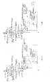
- Figs. 3A and 3B are diagrams showing a third configuration principle of the semiconductor device current detector circuit according to the embodiment of the invention.
- the current detector circuit 2 according to the embodiment of the invention is configured of the current-voltage conversion circuit 24, the first variable voltage source circuit 22, a second variable voltage source circuit 23, and the output level regulator 25.
- the current-voltage conversion circuit, first variable voltage source circuit, and second variable voltage source circuit are connected in series. Also, the current detector circuit 2 is connected between the sense terminal S and main terminal M of the power semiconductor element 1 shown in an upper portion of Fig. 3A . Furthermore, the output of the current-voltage conversion circuit 24 is input into the output (gain) regulator 221 of the first variable voltage source circuit 22. Also, the input side of the output level regulator 25 is connected to the output side of the current-voltage conversion circuit 24.
- the configuration of the power semiconductor element 1 shown in the upper portion of Fig. 3A is basically the same as that shown in Figs. 13A and 13B .
- the gain Kg is set by the output (gain) regulator 221 in such a way that the output voltage of the first variable voltage source circuit 22 is changed in accordance with the current detected by the current-voltage conversion circuit 24, and the offset Ko is set by an output (offset) regulator 231 in such a way that the output voltage of the second variable voltage source circuit 23 is changed.
- Kg is set as a parameter correcting a difference in internal resistance
- Ko as a parameter correcting a difference in internal threshold voltage.
- the gain Kg and offset Ko function as a simulated resistance and offset voltage respectively, it is possible to correct a difference in characteristics between the main region and sensing region by regulating so that Rm ⁇ 0 ⁇ Rs ⁇ 0 + Kg Vthm ⁇ 0 ⁇ Vths ⁇ 0 + Ko
- Rm0 is the internal resistance of the main region
- Rs0 is the internal resistance of the sensing region
- Vthm0 is the threshold voltage of the main region
- Vths0 is the threshold voltage of the sensing region.
- the gain Kg and offset Ko can be set to either a positive or negative polarity.
- Fig. 3B it is also possible to set the gain Kg and offset Ko to a positive or negative polarity using a digital signal (output setting signal) output from the CPU 3 provided externally.
- the output setting signal output from the CPU 3 is applied to the output (gain) regulator 221 and output (offset) regulator 231 in a serial form or parallel form.
- Figs. 4A and 4B are diagrams showing a fourth configuration principle of the semiconductor device current detector circuit according to the embodiment of the invention.
- the current detector circuit 2 according to the embodiment of the invention is configured of the current-voltage conversion circuit 24, the variable voltage source circuit 23, a variable resistor 26, and the output level regulator 25.
- variable resistor 26, current-voltage conversion circuit 24, and variable voltage source circuit 23 are connected in series. Also, the current detector circuit 2 is connected between the sense terminal S and main terminal M of the power semiconductor element 1 shown in an upper portion of Fig. 4A . Furthermore, the input side of the output level regulator 25 is connected to the output side of the current-voltage conversion circuit 24.
- the configuration of the power semiconductor element 1 shown in the upper portion of Fig. 4A is basically the same as that shown in Figs. 13A and 13B .
- the offset Ko of the output (offset) regulator 231 is set for the output voltage of the variable voltage source circuit 23, and furthermore, for a resistance value Rc of the variable resistor 26.
- Ko is set as a parameter correcting a difference in internal threshold voltage.
- Rc and offset Ko function as a resistance and simulated offset voltage respectively, it is possible to correct a difference in characteristics between the main region and sensing region by regulating so that Rm ⁇ 0 ⁇ Rs ⁇ 0 + Rc Vthm ⁇ 0 ⁇ Vths ⁇ 0 + Ko
- Rm0 is the internal resistance of the main region
- Rs0 is the internal resistance of the sensing region
- Vthm0 is the threshold voltage of the main region
- Vths0 is the threshold voltage of the sensing region.
- the offset Ko can be set to either a positive or negative polarity.
- a digital signal (offset setting signal) output from the CPU 3 provided externally.
- the offset setting signal output from the CPU 3 is applied to the output regulator 231 in a serial form or parallel form.
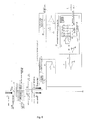
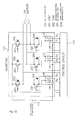
- Fig. 5 is a diagram showing a first working example of the semiconductor device current detector circuit according to the embodiment of the invention.
- the third configuration principle of the semiconductor device current detector circuit according to the embodiment of the invention shown in Figs. 3A and 3B is realized in Fig. 5 .
- the semiconductor device current detector circuit is configured of the current-voltage conversion circuit 24, the first variable voltage source circuit 22, the second variable voltage source circuit 23, and the output level regulator 25.
- the first variable voltage source circuit 22 is configured of two inverting amplifiers and the output (gain) regulator 221.
- the output (gain) regulator 221 is configured of a ladder circuit and a bit signal decoder that carries out a switching in accordance with a bit setting by a digital signal (an example of a 4-bit resolution is shown in the diagram).
- the second variable voltage source circuit 23 is of a configuration wherein a reference potential output integrated circuit (IC) is added to the configuration of the first variable voltage source circuit 22.
- the output voltages of the first variable voltage source circuit 22 and second variable voltage source circuit 23 are added together by an adder circuit (including an operational amplifier and resistors R5 to R7), and connected to a reference potential terminal (positive terminal) of the current-voltage conversion circuit 24.
- the output level regulator 25 is configured of an adder circuit (including an operational amplifier and resistors R2 to R4) , and regulates the gain and offset of the current sensing output.
- the second variable voltage source circuit 23, with an output voltage Vref of the reference potential output IC as an input, can output -Vref to Vref (the offset Ko -1 to 1) in accordance with the setting of a bit signal.
- the gain Kg and offset Ko are regulated in accordance with the relationship between the internal resistance Rm0 of the main region and the internal resistance Rs0 of the sensing region.
- the gain Kg and offset Ko are regulated in such a way that Rm ⁇ 0 ⁇ Rs ⁇ 0 + R ⁇ 7 / R ⁇ 5 ⁇ R ⁇ 1 ⁇ Kg Vthm ⁇ 0 ⁇ Vths ⁇ 0 + R ⁇ 7 / R ⁇ 6 ⁇ Vref ⁇ Ko
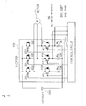
- FIG. 6 is a diagram showing a second working example of the semiconductor device current detector circuit according to the embodiment of the invention.
- the fourth configuration principle of the semiconductor device current detector circuit according to the embodiment of the invention shown in Figs. 4A and 4B is realized in Fig. 6 .
- the semiconductor device current detector circuit is configured of the current-voltage conversion circuit 24, the variable voltage source circuit 23, the variable resistor 26, and the output level regulator 25.
- the output level regulator 25 is configured of an adder circuit (including the operational amplifier and resistors R2 to R4) , and regulates the gain and offset of the current sensing output.
- Vrc R ⁇ 7 / R ⁇ 6 ⁇ Vref ⁇ Ko
- the sense terminal voltage Vs Rc ⁇ Is + R ⁇ 7 / R ⁇ 6 ⁇ Vref ⁇ Ko
- the offset Ko functions as a simulated offset voltage
- variable resistance value Rc and offset Ko are regulated in such a way that Rm ⁇ 0 ⁇ Rs ⁇ 0 + Rc Vthm ⁇ 0 ⁇ Vths ⁇ 0 + R ⁇ 7 / R ⁇ 6 ⁇ Vref ⁇ Ko .
- Fig. 14 shows a condition wherein the linearity of the Im-Is characteristic is improved.
- Fig. 14 is a diagram showing a condition of an improvement of the linearity of the Im-Is characteristic by the semiconductor device current detector circuit of the invention.
- the ratio between a main current Im and the sense current Is is not constant, and the Im-Is characteristic curves.
- the semiconductor device current detector circuit of the invention when employing the semiconductor device current detector circuit of the invention to carry out a correction of the Im-Is characteristic, it can be seen that the Im-Is characteristic approximates a straight line, and the linearity thereof is improved.
- Fig. 7 is a diagram showing an example of a configuration of an inverter device to which the semiconductor device current detector circuit of the invention is applied.
- the sensing function-equipped IGBT 203 shown in the working examples of the invention, and a sensing function-equipped FWD 204 are applied in a lower arm. That is, the current detector circuit 2 shown in the working examples of the invention is connected to each sense terminal S. In this case, the current detector circuit 2 may be that in either the first working example or second working example.
- Fig. 8 is a diagram showing an example of a configuration of a chopper circuit to which the semiconductor device current detector circuit of the invention is applied.
- the chopper circuit shown in Fig. 8 an example of a DC chopper circuit being shown, the sensing function-equipped IGBT 203 shown in the working examples of the invention, and the sensing function-equipped FWD 204, are applied in a lower arm. That is, the current detector circuit 2 shown in the working examples of the invention is connected to the sense terminal of each of the IGBT 203 and FWD 204. In this case, the current detector circuit 2 may be that in either the first working example or second working example.
- the invention not being limited to the examples of the inverter device and chopper circuit, it is also possible to apply the semiconductor device current detector circuit of the invention to other intelligent power module (IPM) applications.
- IPM intelligent power module
Landscapes
- Physics & Mathematics (AREA)
- General Physics & Mathematics (AREA)
- Measurement Of Current Or Voltage (AREA)
- Inverter Devices (AREA)
- Dc-Dc Converters (AREA)
- Control Of Voltage And Current In General (AREA)
- Power Conversion In General (AREA)
Abstract
Description
- The present invention relates to a power semiconductor device current detector circuit and detection method, and in particular, relates to a current detector circuit and detection method that detect a current flowing through a power semiconductor device such as a diode, thyristor, transistor (bipolar transistor or metal oxide semiconductor field effect transistor (MOSFET)), or insulated gate bipolar transistor (IGBT).
- An IGBT module in which are mounted an IGBT, which is one kind of power semiconductor device, and a free wheeling diode (hereafter called an FWD) is applied to a power conversion device such as an inverter or direct current (DC) chopper circuit.
- Generally, an output current detection is necessary in order to control these power conversion circuits. Normally, two methods are widely employed in the output current detection, which are
- 1: a method using a current detector such as a current transformer or direct current current transformer (DCCT), and
- 2: a method using a current detecting resistor (called a shunt resistor).
-
Fig. 9 is a diagram showing an example of a configuration of a heretofore known three-phase inverter device in which a DCCT is used. The DCCT (also called a direct current current transformer) utilizes a ring-like core and a Hall element, which is a magnetic sensor, as shown inJP-A-2000-134955 Figs. 1 and 18) shown below. Wiring is passed through the core, and the current is detected by detecting magnetism generated when current is passed through the wiring. In aninverter 101 shown inFig. 9 , theDCCT 105 is installed on the output wiring, and the detected current value is input into acontrol circuit 102. -
Fig. 10 is a diagram showing an example of a configuration of a heretofore known three-phase inverter device in which a shunt resistor is used. Ashunt resistor 106 is connected in the lower arm of theinverter 101 shown inFig. 10 . As an output current flows through the lower arm at a timing at which anIGBT 201 of the lower arm comes on, the output current is detected by detecting a voltage drop of theshunt resistor 106 at this time in thecontrol circuit 102. A current detector circuit in which the shunt resistor is used is shown in, for example,JP-A-2003-274667 Figs. 1 ,4 , and7 ) shown below. -
Fig. 11 is a diagram showing an example of a configuration of a heretofore known chopper circuit in which a shunt resistor is used. Theshunt resistor 106 is connected to a ground (GND) line, as shown inFig. 11 , and the voltage drop of theresistor 106 is detected. By detecting the current in this place, thecontrol circuit 102 can detect a current when there is a boost chopper action from a directcurrent power source 103 in the direction of an aluminumelectrolytic capacitor 108, and a current when there is a step down chopper action from the aluminumelectrolytic capacitor 108 in the direction of the directcurrent power source 103. - The heretofore known current detection methods have the kinds of problem indicated below. That is, with the current detection method in which a DCCT is used shown in
Fig. 9 , there are problems in that the price is generally high because the DCCT uses a Hall sensor and a core, and that the output characteristics of the DCCT change due to the ambient temperature. Also, there is a problem in that the size of the detector increases because a core is used, and this restricts the miniaturization of the power conversion device. - Also, with the current detection method in which a shunt resistor is used shown in
Fig. 10 , there is a problem in that, as power loss occurs due to the shunt resistor, the power conversion efficiency of the power conversion device decreases. Furthermore, there is a problem in that the size of the resistor itself increases in order to tolerate a large loss, and this restricts the miniaturization of the conversion device. - However, there are cases in which a current detecting function called a "sensing function-equipped power semiconductor device" is installed in a diode, thyristor, transistor, or the like, which are power semiconductor devices. For example, among IGBTs or FWDs configuring an inverter device, there are ones called "sense IGBTs" and "sense FWDs" equipped with a current detecting function. Hereafter, the function will be described with a "sense IGBT" as an example.
- Normally, an IGBT is configured of a few thousand to a few tens of thousands of cells of the same structure. One portion of these is utilized as current detecting cells. In this case, an IGBT formed from the current detecting portion of the cells is called a "sensing region", and an IGBT formed from the other cells a "main region". Then, generally, it is often the case that a ratio Nm/Ns between a main region cell quantity Nm (Nm is an integer) and a sensing region cell quantity Ns (Ns is an integer) is set at a few thousand to one. Although the main region and sensing region share a collector terminal, emitter terminals are divided into a main emitter terminal (hereafter called a main terminal) and a current detecting emitter terminal (hereafter called a sense terminal). An IGBT with this kind of configuration is represented by the kind of symbolic circuit shown in
Fig. 13A . Also, an equivalent circuit thereof is represented as inFig. 13B . - In the case of a free wheeling diode (FWD) too, one portion of the chip is divided off for current detecting in the same way, and anode terminals are divided into a main anode terminal (hereafter, a main terminal) and a current detecting anode terminal (hereafter, a sense terminal).
- With an existing intelligent power module (IPM), an example has been reported wherein the function of the sense IGBT is used for detecting an overcurrent. That is, in
JP-A-10-32476 Figs. 8 and9 ) shown below, it is determined that an overcurrent is flowing through the main region when the current flowing through the sensing region exceeds a predetermined value. - Technologies of detecting current utilizing the sensing region are also proposed in
JP-A-2000-134955 Figs. 1 and 18) andJP-A-2003-274667 Figs. 1 ,4 , and7 ) shown below. These technologies will be described usingFig. 12 .
In principle, a current in accordance with the ratio Nm/Ns between the cell quantities flows through the sense terminal (refer to Equation 1). -

Herein, Im is the main current (the current flowing through the main IGBT), Is is the sense current (the current flowing through the sense IGBT), Nm is the main region cell quantity, and Ns is the sensing region cell quantity.
Therefore, a shunt resistor Rs is connected to the sense terminal as inFig. 12 , a sense current Is is detected, and the main current is calculated based onEquation 2 below. -

Although there has been a problem in that resistor loss increases when detecting the main current Im with the shunt resistor Rs, with this method, the shunt resistor loss is small, and consequently, the problems of a decrease in efficiency and an increase in size of the resistor are eliminated. - However, with this method, current detecting accuracy is a problem. That is, in general, a current detecting accuracy of one to two percent is required in an inverter control. However, as the accuracy is low, the method using the sensing region cannot be put to practical use.
- The following two points are included as reasons for the accuracy being low. That is,
a: a factor caused by differences in characteristics between the main region and sensing region.
That the current ratio is proportional to the cell quantity ratio is based on the premise that the characteristics of each cell of the main region and sensing region are the same. However, as there is actually variation in the characteristics, the ratio between the main current and sense current is not constant. When illustrating this on a graph, the relationship between the main current and sense current is not linear (refer to the characteristics before correction inFig. 14 ). - It can be thought that the difference in characteristics is approximately the difference between threshold voltages Vthm0 and Vths0, and between internal resistances Rm0 and Rs0, of each IGBT.
b: A factor caused by the effect of the shunt resistor.
A voltage drop occurs when a current flows through the shunt resistor Rs connected to the sense terminal. For this reason, a difference occurs between the main terminal potential and sense terminal potential, and the ratio between the main current and sense current is not constant. - Bearing in mind the problems of the related art, the invention has an object of solving the three problems shown below. That is,
1. to reduce an increase in size and increase in loss of the current detector when using a direct current transformer (DCCT) or shunt resistor (for detecting the main current).
2. To ensure that no decrease in current detection accuracy occurs when utilizing a sensing function-equipped power semiconductor device (semiconductor device).
3. To achieve a digital control of a correction circuit that improves the current detection accuracy of the sensing function-equipped power semiconductor device (power semiconductor element), and a suppression of the circuit scale. - More specifically, the object is
a: to realize a small current detector circuit with low loss by detecting current using the sensing function of a power semiconductor element.
b: In this case, to correct the linearity of the main current Im and sense current Is, and improve the current detection accuracy.
c: To enable a digital control of a correction circuit that corrects the linearity, with a realizable circuit scale. - In order to achieve the obj ect, a configuration principle of a power semiconductor device current detector circuit of the invention, taking the difference in characteristics between a main region and sensing region to be due to the difference between a threshold voltage and internal resistance of each IGBT, is that the current detector circuit is configured in such a way as to correct the difference between the threshold voltage and internal resistance of each IGBT.
For example, the invention relates to a current detector circuit for a semiconductor device including a power semiconductor element, wherein the power semiconductor element is divided into a main region and a sensing region (current detecting region), including a terminal (main terminal) connected to the main region and a terminal (sense terminal) connected to the sensing region, the current detector circuit being connectable to the sense terminal. The current detector circuit comprises a current detector unit including a terminal into which a current to be detected is input, a terminal that has an input current as an output, and a terminal that outputs detected current information, and a variable voltage source circuit including a control input terminal for controlling an output voltage, and is configured in such a way that the current detector unit and variable voltage source circuit are connected in series, the current information output terminal of the current detector unit is connected to the control input of the variable voltage source circuit, and the current detector unit and variable voltage source circuit connected in series are connectable to the sense terminal and main terminal. The potential of the sense terminal is regulated by regulating the output voltage of the variable voltage source circuit in accordance with the current flowing through the sense terminal, thus correcting a difference in characteristics between the main region and sensing region.
Further embodiments relate to a current detector circuit, wherein the variable voltage source circuit comprises a variable resistor and a second variable voltage source circuit. The variable resistor, current detector unit, and the second variable voltage source circuit are connected in series, wherein the potential of the sense terminal is regulated by regulating the resistance value of the variable resistor and the output of the second variable voltage source circuit based on an output of the current information output terminal of the current detecting unit, thus correcting a difference in characteristics between the main region and sensing region. - Specifically, the current detector circuit is configured in such a way that an already known current is caused to flow through the main region, the current is detected from a sense terminal, and a gain and offset are regulated in order to correct the difference in characteristics between the main region and sensing region in accordance with the detected current. More specifically, the current detector circuit is configured in such a way that an already known current is caused to flow through the main region of the semiconductor device, the current is detected by a current detector unit connected to a sense terminal of the semiconductor device, a deviation in characteristics between the main region and sensing region is detected based on the detected current, and an offset amount and gain amount in an output regulator are regulated in such a way that the characteristics of the two coincide.
- Also, the current detector circuit is configured in such a way that a parameter Kg that corrects a difference in internal resistance, and a parameter Ko that corrects a difference in internal threshold voltage, are set as correction parameters for improving the current detection accuracy of the semiconductor device, and the parameters can be changed from the exterior by a digital signal passing through a serial or parallel signal supply unit.
- Furthermore, an inverter device or chopper circuit configured to include an IGBT and FWD in upper arm and lower arm switching elements is configured in such a way that the IGBT provided in the upper arm is a sensing function-equipped IGBT and the FWD provided in the lower arm is a sensing function-equipped FWD, and the heretofore described current detector circuit is connected to the sense terminals of the sensing function-equipped IGBT and sensing function-equipped FWD.
- According to the invention, it is possible to correct the sense characteristics of a power semiconductor element, and a highly accurate main current calculation is possible utilizing the sensing function. As the main current detection is carried out using the sensing function in this way, it is possible to realize a miniaturization and decrease in loss of the current detector when compared with the heretofore known methods using a direct current current transformer (DCCT) or shunt resistor (for detecting the main current).
- Also, according to the invention, as the setting of the correction parameters can be carried out from the exterior using a serial or parallel signal supply unit, it is possible to realize an application circuit in which the current detector circuit of the invention is mounted in an appropriate circuit scale.
- Also, by applying the current detector circuit of the invention in the lower arm of an inverter device or the lower arm of a chopper circuit, it is possible to accurately detect the output current of the inverter device or chopper circuit.
-
-
Figs. 1A and 1B are diagrams showing a first configuration principle of a semiconductor device and a current detector circuit according to an embodiment of the invention; -
Figs. 2A and 2B are diagrams showing a second configuration principle of the semiconductor device current detector circuit according to the embodiment of the invention; -
Figs. 3A and 3B are diagrams showing a third configuration principle of the semiconductor device current detector circuit according to the embodiment of the invention; -
Figs. 4A and 4B are diagrams showing a fourth configuration principle of the semiconductor device current detector circuit according to the embodiment of the invention; -
Fig. 5 is a diagram showing a first working example of the semiconductor device current detector circuit according to the embodiment of the invention; -
Fig. 6 is a diagram showing a second working example of the semiconductor device current detector circuit according to the embodiment of the invention; -
Fig. 7 is a diagram showing an example of a configuration of an inverter device to which the semiconductor device current detector circuit of the invention is applied; -
Fig. 8 is a diagram showing an example of a configuration of a chopper circuit to which the semiconductor device current detector circuit of the invention is applied; -
Fig. 9 is a diagram showing an example of a configuration of a heretofore known inverter device in which a DCCT is used; -
Fig. 10 is a diagram showing an example of a configuration of a heretofore known inverter device in which a shunt resistor is used; -
Fig. 11 is a diagram showing an example of a configuration of a heretofore known chopper circuit in which a shunt resistor is used; -
Fig. 12 is a diagram showing an example of a configuration of a heretofore known inverter device in which a power semiconductor element is used; -
Figs. 13A and 13B are diagrams showing a symbolic circuit (Fig. 13A ) and equivalent circuit (Fig. 13B ) of a power semiconductor element (for example, an IGBT); and -
Fig. 14 is a diagram showing a condition of an improvement of the linearity of an Im-Is characteristic by the semiconductor device current detector circuit of the invention. - Hereafter, a detailed description will be given of an embodiment of the invention.
A configuration principle of a semiconductor device and a current detector circuit of the invention, taking the difference in characteristics between a main region and sensing region to be due to the difference between a threshold voltage and internal resistance of each IGBT, is that the current detector circuit is configured in such a way as to correct the difference between the threshold voltage and internal resistance of each IGBT. Specifically, the current detector circuit is configured in such a way that an already known current is caused to flow through the main region, the current is detected from a sense terminal, and a gain and offset are regulated in order to correct the difference in characteristics between the main region and sensing region in accordance with the detected current. More specifically, the current detector circuit is configured in such a way that an already known current is caused to flow through the main region of the semiconductor device, the current is detected by a current detector unit connected to a sense terminal of the semiconductor device, a deviation in characteristics between the main region and sensing region is detected based on the detected current, and an offset amount and gain amount in an output regulator are regulated in such a way that the characteristics of the two coincide. A detailed description of this will be given hereafter. By so doing, it is possible to realize a small current detector circuit with low loss. - Next, a detailed description will be given of the semiconductor device current detector circuit according to the embodiment of the invention, but first, a description will be given of a basic configuration of the current detector circuit of the invention, and after that, a description will be given of specific configurations (working examples).
-
Figs. 1A and 1B are diagrams showing a first configuration principle of the semiconductor device and the current detector circuit according to the embodiment of the invention. InFig. 1A , acurrent detector circuit 2 according to the embodiment of the invention is configured of acurrent detection unit 21 and a variablevoltage source circuit 22. Then, thecurrent detection unit 21 and variablevoltage source circuit 22 are connected in series. Also, thecurrent detector circuit 2 is connected between a sense terminal S and a main terminal M of apower semiconductor element 1 shown in an upper portion ofFig. 1A (thepower semiconductor element 1 and thecurrent detector circuit 2 forming together a semiconductor device). The configuration of thepower semiconductor element 1 shown in the upper portion ofFig. 1A is basically the same as that shown inFigs. 13A and 13B . A current sensing output, which is current information detected by thecurrent detection unit 21, is input into anoutput regulator 221 that regulates the output voltage of the variablevoltage source circuit 22. - By configuring in this way, it is possible to fix the potential of the sense terminal S at the output voltage of the variable
voltage source circuit 22. Supposing that the output of the variablevoltage source circuit 22 is 0V, it is possible to fix the potential of the sense terminal S at a ground (GND) potential, regardless of the size of a current flowing as a sense current Is. That is, it is possible to eliminate the effect of a shunt resistor voltage drop, which is a problem with the heretofore known technology. - Furthermore, a gain Kg and offset Ko are set by the
output regulator 221 in such a way that the output voltage of the variablevoltage source circuit 22 is changed in accordance with the current detected by thecurrent detection unit 21. Herein, Kg is set as a parameter correcting a difference in internal resistance, and Ko as a parameter correcting a difference in internal threshold voltage. By so doing, a voltage Vs of the sense terminal S changes in accordance with the current flowing, as follows:
Herein, Kg is the gain, and Ko the offset. As the gain Kg and offset Ko function as a simulated resistance and offset voltage respectively, it is possible to correct a difference in characteristics between the main region and sensing region by regulating so that

Herein, Rm0 is the internal resistance of the main region, Rs0 is the internal resistance of the sensing region, Vthm0 is the threshold voltage of the main region, and Vths0 is the threshold voltage of the sensing region. The gain Kg and offset Ko can be set to either a positive or negative polarity. - Also, as shown in
Fig. 1B , it is also possible to set the gain Kg and offset Ko to a positive or negative polarity using a digital signal (output setting signal) output from a central processing unit (CPU) 3 provided externally. The output setting signal output from the CPU 3 is applied to theoutput regulator 221 in a serial form or parallel form. -
Figs. 2A and 2B are diagrams showing a second configuration principle of the semiconductor device current detector circuit according to the embodiment of the invention. InFig. 2A , thecurrent detector circuit 2 according to the embodiment of the invention is configured of a current-voltage conversion circuit 24, the variablevoltage source circuit 22, and anoutput level regulator 25. Then, the current-voltage conversion circuit 24 and variablevoltage source circuit 22 are connected in series. Also, thecurrent detector circuit 2 is connected between the sense terminal S and main terminal M of thepower semiconductor element 1 shown in an upper portion ofFig. 2A . Furthermore, the output of the current-voltage conversion circuit 24 is input into theoutput regulator 221 of the variablevoltage source circuit 22. Also, the input side of theoutput level regulator 25 is connected to the output side of the current-voltage conversion circuit 24. The configuration of thepower semiconductor element 1 shown in the upper portion ofFig. 2A is basically the same as that shown inFigs. 13A and 13B . - By configuring in this way, it is possible to fix the potential of the sense terminal S at the output voltage of the variable voltage source circuit 22 (because the negative terminal and positive terminal of the operational amplifier are virtually short-circuited). Supposing that the output voltage of the variable
voltage source circuit 22 is 0V, it is possible to fix the potential of the sense terminal S at the GND potential, regardless of the size of the current flowing as the sense current Is. That is, it is possible to eliminate the effect of a shunt resistor voltage drop, which is a problem with the heretofore known technology. - Furthermore, the gain Kg and offset Ko are set by the
output regulator 221 in such a way that the output voltage of the variablevoltage source circuit 22 is changed in accordance with the current detected by the current-voltage conversion circuit 24. As heretofore described, Kg is set as a parameter correcting a difference in internal resistance, and Ko as a parameter correcting a difference in internal threshold voltage. By so doing, the voltage Vs of the sense terminal S changes in accordance with the current flowing, as follows:
Herein, Kg is the gain, and Ko the offset. As the gain Kg and offset Ko function as a simulated resistance and offset voltage respectively, it is possible to correct a difference in characteristics between the main region and sensing region by regulating so that

Herein, Rm0 is the internal resistance of the main region, Rs0 is the internal resistance of the sensing region, Vthm0 is the threshold voltage of the main region, and Vths0 is the threshold voltage of the sensing region. The gain Kg and offset Ko can be set to either a positive or negative polarity. - Also, as shown in
Fig. 2B , it is also possible to set the gain Kg and offset Ko to a positive or negative polarity using a digital signal (output setting signal) output from the CPU 3 provided externally. The output setting signal output from the CPU 3 is applied to theoutput regulator 221 in a serial form or parallel form. -
Figs. 3A and 3B are diagrams showing a third configuration principle of the semiconductor device current detector circuit according to the embodiment of the invention. InFig. 3A , thecurrent detector circuit 2 according to the embodiment of the invention is configured of the current-voltage conversion circuit 24, the first variablevoltage source circuit 22, a second variablevoltage source circuit 23, and theoutput level regulator 25. - The current-voltage conversion circuit, first variable voltage source circuit, and second variable voltage source circuit are connected in series. Also, the
current detector circuit 2 is connected between the sense terminal S and main terminal M of thepower semiconductor element 1 shown in an upper portion ofFig. 3A . Furthermore, the output of the current-voltage conversion circuit 24 is input into the output (gain)regulator 221 of the first variablevoltage source circuit 22. Also, the input side of theoutput level regulator 25 is connected to the output side of the current-voltage conversion circuit 24. The configuration of thepower semiconductor element 1 shown in the upper portion ofFig. 3A is basically the same as that shown inFigs. 13A and 13B . - By configuring in this way, it is possible to fix the potential of the sense terminal S at a voltage wherein the output voltages of the first variable
voltage source circuit 22 and second variablevoltage source circuit 23 are combined (because the negative terminal and positive terminal of the operational amplifier are virtually short-circuited). Supposing that the voltage wherein the output voltages of the first variablevoltage source circuit 22 and second variablevoltage source circuit 23 are combined is 0V, it is possible to fix the potential of the sense terminal S at the GND potential, regardless of the size of the current flowing as the sense current Is. That is, it is possible to eliminate the effect of a shunt resistor voltage drop, which is a problem with the heretofore known technology. - Furthermore, the gain Kg is set by the output (gain)
regulator 221 in such a way that the output voltage of the first variablevoltage source circuit 22 is changed in accordance with the current detected by the current-voltage conversion circuit 24, and the offset Ko is set by an output (offset)regulator 231 in such a way that the output voltage of the second variablevoltage source circuit 23 is changed. As heretofore described, Kg is set as a parameter correcting a difference in internal resistance, and Ko as a parameter correcting a difference in internal threshold voltage. By so doing, the voltage Vs of the sense terminal S changes in accordance with the current flowing, as follows:
Herein, Kg is the gain, and Ko the offset. As the gain Kg and offset Ko function as a simulated resistance and offset voltage respectively, it is possible to correct a difference in characteristics between the main region and sensing region by regulating so that

Herein, Rm0 is the internal resistance of the main region, Rs0 is the internal resistance of the sensing region, Vthm0 is the threshold voltage of the main region, and Vths0 is the threshold voltage of the sensing region. The gain Kg and offset Ko can be set to either a positive or negative polarity. - Also, as shown in
Fig. 3B , it is also possible to set the gain Kg and offset Ko to a positive or negative polarity using a digital signal (output setting signal) output from the CPU 3 provided externally. The output setting signal output from the CPU 3 is applied to the output (gain)regulator 221 and output (offset)regulator 231 in a serial form or parallel form. -
Figs. 4A and 4B are diagrams showing a fourth configuration principle of the semiconductor device current detector circuit according to the embodiment of the invention. InFig. 4A , thecurrent detector circuit 2 according to the embodiment of the invention is configured of the current-voltage conversion circuit 24, the variablevoltage source circuit 23, avariable resistor 26, and theoutput level regulator 25. - The
variable resistor 26, current-voltage conversion circuit 24, and variablevoltage source circuit 23 are connected in series. Also, thecurrent detector circuit 2 is connected between the sense terminal S and main terminal M of thepower semiconductor element 1 shown in an upper portion ofFig. 4A . Furthermore, the input side of theoutput level regulator 25 is connected to the output side of the current-voltage conversion circuit 24. The configuration of thepower semiconductor element 1 shown in the upper portion ofFig. 4A is basically the same as that shown inFigs. 13A and 13B . - By configuring in this way, the offset Ko of the output (offset)
regulator 231 is set for the output voltage of the variablevoltage source circuit 23, and furthermore, for a resistance value Rc of thevariable resistor 26. Herein, Ko is set as a parameter correcting a difference in internal threshold voltage. By so doing, the voltage Vs of the sense terminal S changes in accordance with the current flowing, as follows:
Herein, Rc is the resistance value of the variable resistor, and Ko the offset. As the resistance Rc and offset Ko function as a resistance and simulated offset voltage respectively, it is possible to correct a difference in characteristics between the main region and sensing region by regulating so that

Herein, Rm0 is the internal resistance of the main region, Rs0 is the internal resistance of the sensing region, Vthm0 is the threshold voltage of the main region, and Vths0 is the threshold voltage of the sensing region. The offset Ko can be set to either a positive or negative polarity. - Also, as shown in
Fig. 4B , it is also possible to set the offset Ko to a positive or negative polarity using a digital signal (offset setting signal) output from the CPU 3 provided externally. The offset setting signal output from the CPU 3 is applied to theoutput regulator 231 in a serial form or parallel form. -
Fig. 5 is a diagram showing a first working example of the semiconductor device current detector circuit according to the embodiment of the invention. The third configuration principle of the semiconductor device current detector circuit according to the embodiment of the invention shown inFigs. 3A and 3B is realized inFig. 5 . - In the first working example of the invention shown in
Fig. 5 , the semiconductor device current detector circuit according to the embodiment of the invention is configured of the current-voltage conversion circuit 24, the first variablevoltage source circuit 22, the second variablevoltage source circuit 23, and theoutput level regulator 25. - The first variable
voltage source circuit 22 is configured of two inverting amplifiers and the output (gain)regulator 221. The output (gain)regulator 221 is configured of a ladder circuit and a bit signal decoder that carries out a switching in accordance with a bit setting by a digital signal (an example of a 4-bit resolution is shown in the diagram). The second variablevoltage source circuit 23 is of a configuration wherein a reference potential output integrated circuit (IC) is added to the configuration of the first variablevoltage source circuit 22. The output voltages of the first variablevoltage source circuit 22 and second variablevoltage source circuit 23 are added together by an adder circuit (including an operational amplifier and resistors R5 to R7), and connected to a reference potential terminal (positive terminal) of the current-voltage conversion circuit 24. Theoutput level regulator 25 is configured of an adder circuit (including an operational amplifier and resistors R2 to R4) , and regulates the gain and offset of the current sensing output. - Next, a description will be given of the action of the semiconductor device current detector circuit according to the first working example of the invention, but as the principle of the action has already been illustrated in
Figs. 3A and 3B , the description here will be confined to simply adding a small supplement. - The first variable
voltage source circuit 22, with an output voltage Vi of the current-voltage conversion circuit 24 as an input, can output -Vi to Vi (the gain Kg = -1 to 1) in accordance with the setting of a bit signal. The second variablevoltage source circuit 23, with an output voltage Vref of the reference potential output IC as an input, can output -Vref to Vref (the offset Ko = -1 to 1) in accordance with the setting of a bit signal. - The gain Kg and offset Ko are regulated in accordance with the relationship between the internal resistance Rm0 of the main region and the internal resistance Rs0 of the sensing region. At this time, an output wherein the outputs of the first variable
voltage source circuit 22 and second variablevoltage source circuit 23 are added together (the added output is added to the positive terminal (reference terminal) of the operational amplifier provided in the current-voltage conversion circuit 24 and, as the output is added to the virtually short-circuited negative terminal, the result is that the output becomes the potential of the sense terminal S) is
Vs = (R7/R5) x (R1 x Is) x Kg + (R7/R6) x Vref x Ko = {(R7/R5) x R1 x Kg} x Is + {(R7/R6) x Vref x Ko}, and the gain Kg and offset Ko function as a simulated resistance and offset voltage respectively. - Herein, the gain Kg and offset Ko are regulated in such a way that


- By so doing, it is possible to correct a difference in characteristics between the main region and sensing region, and linearize an Im-Is characteristic.
Fig. 6 is a diagram showing a second working example of the semiconductor device current detector circuit according to the embodiment of the invention. The fourth configuration principle of the semiconductor device current detector circuit according to the embodiment of the invention shown inFigs. 4A and 4B is realized inFig. 6 . - In the second working example of the invention shown in
Fig. 6 , the semiconductor device current detector circuit according to the embodiment of the invention is configured of the current-voltage conversion circuit 24, the variablevoltage source circuit 23, thevariable resistor 26, and theoutput level regulator 25. - The
output level regulator 25 is configured of an adder circuit (including the operational amplifier and resistors R2 to R4) , and regulates the gain and offset of the current sensing output.
Next, a description will be given of the action of the semiconductor device current detector circuit according to the second working example of the invention, but as the principle of the action has already been illustrated inFigs. 4A and 4B , the description here will be confined to simply adding a small supplement. - Comparing the internal resistance Rm0 of the main region and internal resistance Rs0 of the sensing region, when

the voltage Vs of the sense terminal S is
and the sense terminal voltage Vs rises in proportion to an increase of the current. - Also, when the offset Ko is regulated, a potential Vrc of the terminal of the
variable resistor 26 connected to the current-voltage conversion circuit 24 becomes
as a result of which the sense terminal voltage Vs becomes
and the offset Ko functions as a simulated offset voltage. - Herein, the variable resistance value Rc and offset Ko are regulated in such a way that


- By so doing, it is possible to correct a difference in characteristics between the main region and sensing region, and linearize the Im-Is characteristic.
Fig. 14 shows a condition wherein the linearity of the Im-Is characteristic is improved.Fig. 14 is a diagram showing a condition of an improvement of the linearity of the Im-Is characteristic by the semiconductor device current detector circuit of the invention. As shown inFig. 14 , before the correction of the Im-Is characteristic, the ratio between a main current Im and the sense current Is is not constant, and the Im-Is characteristic curves. As opposed to this, when employing the semiconductor device current detector circuit of the invention to carry out a correction of the Im-Is characteristic, it can be seen that the Im-Is characteristic approximates a straight line, and the linearity thereof is improved. -
Fig. 7 is a diagram showing an example of a configuration of an inverter device to which the semiconductor device current detector circuit of the invention is applied. In the inverter device shown inFig. 7 , the sensing function-equippedIGBT 203 shown in the working examples of the invention, and a sensing function-equippedFWD 204, are applied in a lower arm. That is, thecurrent detector circuit 2 shown in the working examples of the invention is connected to each sense terminal S. In this case, thecurrent detector circuit 2 may be that in either the first working example or second working example. - By configuring in this way, it is possible to detect a lower arm current in a three-phase inverter device, and by so doing, it is possible to accurately detect the output current of the inverter device. As the rest of the configuration is the same as that of the heretofore known inverter device shown in
Fig. 10 , a description thereof will be omitted. -
Fig. 8 is a diagram showing an example of a configuration of a chopper circuit to which the semiconductor device current detector circuit of the invention is applied. In the chopper circuit shown inFig. 8 , an example of a DC chopper circuit being shown, the sensing function-equippedIGBT 203 shown in the working examples of the invention, and the sensing function-equippedFWD 204, are applied in a lower arm. That is, thecurrent detector circuit 2 shown in the working examples of the invention is connected to the sense terminal of each of theIGBT 203 andFWD 204. In this case, thecurrent detector circuit 2 may be that in either the first working example or second working example. - By configuring in this way, it is possible to detect a lower arm current of the chopper circuit, and by so doing, it is possible to accurately detect the output current of the chopper circuit. As the rest of the configuration is the same as that of the heretofore known chopper circuit shown in
Fig. 11 , a description thereof will be omitted. - The invention not being limited to the examples of the inverter device and chopper circuit, it is also possible to apply the semiconductor device current detector circuit of the invention to other intelligent power module (IPM) applications.
Claims (8)
- A current detector circuit for a semiconductor device including a power semiconductor element, wherein the power semiconductor element is divided into a main region and a sensing region (current detecting region), including a terminal (main terminal) connected to the main region and a terminal (sense terminal) connected to the sensing region,
the current detector circuit being connectable to the sense terminal,
the current detector circuit comprising:a current detector unit including a terminal into which a current to be detected is input, a terminal that has an input current as an output, and a terminal that outputs detected current information; anda variable voltage source circuit including a control input terminal for controlling an output voltage,and being configured in such a way thatthe current detector unit and variable voltage source circuit are connected in series,the current information output terminal of the current detector unit is connected to the control input of the variable voltage source circuit, andthe current detector unit and variable voltage source circuit connected in series are connectable to the sense terminal and main terminal, whereinthe potential of the sense terminal is regulated by regulating the output voltage of the variable voltage source circuit in accordance with the current flowing through the sense terminal, thus correcting a difference in characteristics between the main region and sensing region. - The current detector circuit according to claim 1, configured in such a way that
the variable voltage source circuit comprises a first variable voltage source circuit and a second variable voltage source circuit,
the current detector unit, first variable voltage source circuit, and second variable voltage source circuit are connected in series, and
the current information output terminal of the current detector unit is connected to the control input of the first variable voltage source circuit, wherein
the potential of the sense terminal is regulated by regulating the output voltage of the first variable voltage source circuit and regulating the output voltage of the second variable voltage source circuit in accordance with the current flowing through the sense terminal, thus correcting a difference in characteristics between the main region and sensing region. - The current detector circuit according to claim 1, the variable voltage source circuit comprising a variable resistor and a second variable voltage source circuit,
the variable resistor, current detector unit, and the second variable voltage source circuit being connected in series, wherein
the potential of the sense terminal is regulated by regulating the resistance value of the variable resistor and the output of the second variable voltage source circuit based on an output of the current information output terminal of the current detecting unit, thus correcting a difference in characteristics between the main region and sensing region. - The current detector circuit according to claim 1, wherein
the current detector unit is a current-voltage conversion circuit. - The current detector circuit according to claim 1, comprising:a reference voltage input terminal;a gain regulating function controllable by a digital signal supplied from the exterior; anda variable voltage source circuit that can output a voltage wherein a gain amount controlled and set by the digital signal is multiplied by the reference voltage.
- An inverter device including an IGBT and FWD in upper arm and lower arm switching elements, wherein the IGBT provided in the lower arm is a sensing function-equipped IGBT and the FWD provided in the lower arm is a sensing function-equipped FWD, and the current detector circuit according to claim 1 is connected to each sense terminal of the sensing function-equipped IGBT and sensing function-equipped FWD.
- A chopper circuit including an IGBT and FWD in upper arm and lower arm switching elements, wherein the IGBT provided in the lower arm is a sensing function-equipped IGBT and the FWD provided in the lower arm is a sensing function-equipped FWD, and the current detector circuit according to claim 1 is connected to each sense terminal of the sensing function-equipped IGBT and sensing function-equipped FWD.
- A current detection method of a semiconductor device including a power semiconductor element, wherein the power semiconductor element is divided into a main region and a sensing region (current detecting region), including a terminal (main terminal) connected to the main region and a terminal (sense terminal) connected to the sensing region, and a current detector circuit being connectable to the sense terminal, comprising:an already known current being caused to flow through the main region, the current being detected by a current detector unit in the current detector circuit connected to the sense terminal, a deviation in characteristics between the main region and sensing region being detected based on the detected current, and an offset amount and gain amount in an output regulator provided in the current detector circuit being regulated in such a way that the characteristics of the two coincide.
Applications Claiming Priority (1)
| Application Number | Priority Date | Filing Date | Title |
|---|---|---|---|
| JP2010228103A JP5724281B2 (en) | 2010-10-08 | 2010-10-08 | Current detection circuit for power semiconductor devices |
Publications (2)
| Publication Number | Publication Date |
|---|---|
| EP2439545A2 true EP2439545A2 (en) | 2012-04-11 |
| EP2439545A3 EP2439545A3 (en) | 2017-12-06 |
Family
ID=44905462
Family Applications (1)
| Application Number | Title | Priority Date | Filing Date |
|---|---|---|---|
| EP11184204.3A Withdrawn EP2439545A3 (en) | 2010-10-08 | 2011-10-06 | Power semiconductor device current detector circuit and detection method |
Country Status (4)
| Country | Link |
|---|---|
| US (1) | US8659864B2 (en) |
| EP (1) | EP2439545A3 (en) |
| JP (1) | JP5724281B2 (en) |
| CN (1) | CN102565502B (en) |
Families Citing this family (18)
| Publication number | Priority date | Publication date | Assignee | Title |
|---|---|---|---|---|
| JP5664536B2 (en) * | 2011-12-19 | 2015-02-04 | 株式会社デンソー | Current detection circuit and semiconductor integrated circuit device |
| US9291678B2 (en) * | 2012-05-31 | 2016-03-22 | Deere & Company | Method and controller for an electric motor with switch testing |
| KR101350689B1 (en) * | 2012-07-31 | 2014-01-13 | 삼성전기주식회사 | Driving apparatus having current detection and driving apparatus for motor having current detection |
| WO2014097739A1 (en) | 2012-12-17 | 2014-06-26 | 富士電機株式会社 | Semiconductor device and current detection circuit using said semiconductor device |
| JP5979570B2 (en) * | 2013-07-10 | 2016-08-24 | パナソニックIpマネジメント株式会社 | Semiconductor device and inverter using the same |
| JP2015119594A (en) * | 2013-12-19 | 2015-06-25 | トヨタ自動車株式会社 | Drive control device for semiconductor device |
| DE102014211984A1 (en) * | 2014-06-23 | 2015-12-24 | Robert Bosch Gmbh | Method and apparatus for current sensing of small currents |
| KR20170034166A (en) | 2015-09-18 | 2017-03-28 | 삼성전자주식회사 | Semiconductor chip and semiconductor package having the same |
| JP6950200B2 (en) * | 2017-03-02 | 2021-10-13 | 株式会社デンソー | Power converter and power converter adjustment method |
| JP7008478B2 (en) * | 2017-11-15 | 2022-01-25 | 新日本無線株式会社 | Current sense amplifier circuit and switching power supply |
| JP6989462B2 (en) | 2018-08-24 | 2022-01-05 | 株式会社東芝 | Current detection circuit |
| TWI708064B (en) | 2018-09-25 | 2020-10-21 | 財團法人工業技術研究院 | Test system, test method for the test system, and test carrier |
| CN110954842B (en) * | 2018-09-25 | 2022-04-05 | 财团法人工业技术研究院 | Test system, test method for test system and test carrier |
| CN109683007B (en) * | 2018-11-29 | 2022-04-19 | Oppo(重庆)智能科技有限公司 | Current testing mold, system and method |
| CN109655776B (en) * | 2019-01-15 | 2021-06-18 | 昆明理工大学 | Broadband characteristic testing system and method of DC current transformer for grounding pole line |
| CN113092979B (en) * | 2021-04-16 | 2021-11-02 | 全球能源互联网研究院有限公司 | A MMC working condition power semiconductor device test circuit and control method |
| CN113296025B (en) * | 2021-07-26 | 2021-10-22 | 佛山市联动科技股份有限公司 | Precise high-voltage micro leakage current measuring module for ATE (automatic test equipment) test |
| JP2024030798A (en) * | 2022-08-25 | 2024-03-07 | 株式会社Gsユアサ | Detection device, power storage device, and detection method |
Citations (3)
| Publication number | Priority date | Publication date | Assignee | Title |
|---|---|---|---|---|
| JPH1032476A (en) | 1996-05-14 | 1998-02-03 | Fuji Electric Co Ltd | Overcurrent protection circuit |
| JP2000134955A (en) | 1998-10-26 | 2000-05-12 | Hitachi Ltd | Inverter device and switching module for inverter device |
| JP2003274667A (en) | 2002-03-14 | 2003-09-26 | Toshiba Corp | Power module for three-phase inverter and three-phase motor drive system |
Family Cites Families (40)
| Publication number | Priority date | Publication date | Assignee | Title |
|---|---|---|---|---|
| US4893158A (en) | 1987-06-22 | 1990-01-09 | Nissan Motor Co., Ltd. | MOSFET device |
| JP2523678B2 (en) | 1987-09-08 | 1996-08-14 | 日産自動車株式会社 | MOSFET with overcurrent protection function |
| JP2806503B2 (en) | 1988-11-11 | 1998-09-30 | 三菱電機株式会社 | Semiconductor element short-circuit protection circuit |
| JPH0752370B2 (en) * | 1988-12-26 | 1995-06-05 | 株式会社日立製作所 | Current detection circuit for semiconductor devices |
| JP2940843B2 (en) * | 1992-01-23 | 1999-08-25 | 三菱電機株式会社 | Overcurrent protection method and device, and overcurrent detection device |
| JPH05259853A (en) | 1992-03-12 | 1993-10-08 | Hitachi Ltd | Current limit circuit |
| JPH05276761A (en) * | 1992-03-19 | 1993-10-22 | Hitachi Ltd | Method and circuit for detecting overcurrent in power semiconductor element and inverter using the same |
| JP3084982B2 (en) * | 1992-11-25 | 2000-09-04 | 富士電機株式会社 | Semiconductor device |
| JPH07146722A (en) | 1993-10-01 | 1995-06-06 | Fuji Electric Co Ltd | Overcurrent protection device for transistor |
| JPH08316807A (en) * | 1995-05-15 | 1996-11-29 | Fuji Electric Co Ltd | Current detector |
| JP3125622B2 (en) * | 1995-05-16 | 2001-01-22 | 富士電機株式会社 | Semiconductor device |
| JPH09172359A (en) | 1995-12-19 | 1997-06-30 | Toshiba Corp | Gate circuit of voltage-driven semiconductor switching device |
| EP0808025B1 (en) * | 1996-05-17 | 2004-11-10 | Denso Corporation | Load actuation circuit |
| US6180966B1 (en) | 1997-03-25 | 2001-01-30 | Hitachi, Ltd. | Trench gate type semiconductor device with current sensing cell |
| JP3914328B2 (en) | 1997-03-25 | 2007-05-16 | 株式会社ルネサステクノロジ | Trench gate semiconductor device with current detection cell and power conversion device |
| JPH11235015A (en) | 1998-02-13 | 1999-08-27 | Toshiba Corp | Voltage-driven power semiconductor device and gate control method thereof |
| JP2001211059A (en) * | 2000-01-26 | 2001-08-03 | Toshiba Corp | Overcurrent protection circuit for semiconductor switch element |
| US6717785B2 (en) * | 2000-03-31 | 2004-04-06 | Denso Corporation | Semiconductor switching element driving circuit |
| JP4219567B2 (en) * | 2001-04-03 | 2009-02-04 | 三菱電機株式会社 | Semiconductor device |
| JP2004045213A (en) * | 2002-07-11 | 2004-02-12 | Yazaki Corp | Current detector |
| JP2004312924A (en) * | 2003-04-09 | 2004-11-04 | Mitsubishi Electric Corp | Driver circuit for semiconductor device |
| JP4622214B2 (en) | 2003-07-30 | 2011-02-02 | トヨタ自動車株式会社 | Semiconductor device having current sensing function |
| JP4545603B2 (en) * | 2005-01-28 | 2010-09-15 | 三菱電機株式会社 | Power semiconductor device |
| JP2006271098A (en) | 2005-03-24 | 2006-10-05 | Hitachi Ltd | Power converter |
| US7365559B2 (en) * | 2005-05-03 | 2008-04-29 | Potentia Semiconductor Inc. | Current sensing for power MOSFETs |
| JP2007049870A (en) | 2005-08-12 | 2007-02-22 | Fuji Electric Device Technology Co Ltd | Power semiconductor module |
| JP4668836B2 (en) * | 2006-05-09 | 2011-04-13 | ローム株式会社 | CHARGE CONTROL CIRCUIT AND CHARGE CIRCUIT AND ELECTRONIC DEVICE USING THE SAME |
| JP2008005217A (en) | 2006-06-22 | 2008-01-10 | Fuji Electric Device Technology Co Ltd | Analog circuit using operational amplifier |
| JP4905208B2 (en) | 2006-10-25 | 2012-03-28 | 株式会社デンソー | Overcurrent detection circuit |
| JP4924086B2 (en) * | 2007-02-21 | 2012-04-25 | 三菱電機株式会社 | Semiconductor device |
| JP4778467B2 (en) | 2007-04-02 | 2011-09-21 | ルネサスエレクトロニクス株式会社 | Trench gate type semiconductor device |
| JP4752811B2 (en) * | 2007-06-06 | 2011-08-17 | 日産自動車株式会社 | Drive circuit for voltage-driven element |
| US7960997B2 (en) * | 2007-08-08 | 2011-06-14 | Advanced Analogic Technologies, Inc. | Cascode current sensor for discrete power semiconductor devices |
| DE102008045410B4 (en) | 2007-09-05 | 2019-07-11 | Denso Corporation | Semiconductor device with IGBT with built-in diode and semiconductor device with DMOS with built-in diode |
| JP5012737B2 (en) | 2007-09-05 | 2012-08-29 | 株式会社デンソー | Semiconductor device |
| JP5136144B2 (en) * | 2008-03-21 | 2013-02-06 | 株式会社デンソー | Load current supply circuit |
| JP2010004728A (en) | 2008-05-23 | 2010-01-07 | Denso Corp | Power conversion apparatus |
| JP5200975B2 (en) * | 2009-02-06 | 2013-06-05 | 株式会社デンソー | Current detection device for power conversion circuit |
| JP5412873B2 (en) | 2009-02-25 | 2014-02-12 | トヨタ自動車株式会社 | Semiconductor device and current measuring method of semiconductor device |
| US7852148B2 (en) * | 2009-03-27 | 2010-12-14 | Semiconductor Components Industries, Llc | Method of forming a sensing circuit and structure therefor |
-
2010
- 2010-10-08 JP JP2010228103A patent/JP5724281B2/en not_active Expired - Fee Related
-
2011
- 2011-09-23 US US13/243,931 patent/US8659864B2/en not_active Expired - Fee Related
- 2011-09-30 CN CN201110310819.4A patent/CN102565502B/en not_active Expired - Fee Related
- 2011-10-06 EP EP11184204.3A patent/EP2439545A3/en not_active Withdrawn
Patent Citations (3)
| Publication number | Priority date | Publication date | Assignee | Title |
|---|---|---|---|---|
| JPH1032476A (en) | 1996-05-14 | 1998-02-03 | Fuji Electric Co Ltd | Overcurrent protection circuit |
| JP2000134955A (en) | 1998-10-26 | 2000-05-12 | Hitachi Ltd | Inverter device and switching module for inverter device |
| JP2003274667A (en) | 2002-03-14 | 2003-09-26 | Toshiba Corp | Power module for three-phase inverter and three-phase motor drive system |
Also Published As
| Publication number | Publication date |
|---|---|
| CN102565502B (en) | 2016-03-30 |
| US8659864B2 (en) | 2014-02-25 |
| JP5724281B2 (en) | 2015-05-27 |
| EP2439545A3 (en) | 2017-12-06 |
| CN102565502A (en) | 2012-07-11 |
| JP2012085407A (en) | 2012-04-26 |
| US20120086424A1 (en) | 2012-04-12 |
Similar Documents
| Publication | Publication Date | Title |
|---|---|---|
| US8659864B2 (en) | Power semiconductor device current detector circuit and detection method | |
| EP2444817B1 (en) | Current detection circuit for a power semiconductor device | |
| JP4924086B2 (en) | Semiconductor device | |
| US8598942B2 (en) | Current correction circuit for power semiconductor device and current correction method | |
| KR102649093B1 (en) | Power conversion device and semiconductor device | |
| US10374594B2 (en) | Semiconductor device | |
| US10193323B2 (en) | Semiconductor device | |
| JP6070841B2 (en) | Overcurrent detection circuit | |
| US9203393B2 (en) | Semiconductor apparatus | |
| US20110248702A1 (en) | Current detection circuit including electrostatic capacitor and rectifying element for increasing gate voltage of protecting mosfet | |
| US9477251B2 (en) | Reference voltage circuit | |
| US10459468B1 (en) | Load current sense circuit | |
| CN102622033A (en) | Voltage regulator | |
| CN110739941B (en) | Semiconductor device with a semiconductor device having a plurality of semiconductor chips | |
| CN110365192B (en) | Temperature detection device | |
| US11387642B2 (en) | Overcurrent sense control of semiconductor device | |
| JP5834396B2 (en) | Current detection circuit for power semiconductor devices | |
| US8971000B2 (en) | Leak current absorption circuit, voltage generating circuit, power supply apparatus, and vehicle | |
| CN108768139A (en) | Current detecting error compensating method and circuit in a kind of pressure-drop type power stage circuit | |
| CN105874690A (en) | Power semiconductor element current detection device | |
| US20260113032A1 (en) | Power semiconductor device | |
| US20240313759A1 (en) | On-state voltage measurement circuit | |
| CN117762182A (en) | Circuit with current protection | |
| RU51311U1 (en) | ELECTRONIC EQUIPMENT PROTECTION SCHEME |
Legal Events
| Date | Code | Title | Description |
|---|---|---|---|
| AK | Designated contracting states |
Kind code of ref document: A2 Designated state(s): AL AT BE BG CH CY CZ DE DK EE ES FI FR GB GR HR HU IE IS IT LI LT LU LV MC MK MT NL NO PL PT RO RS SE SI SK SM TR |
|
| AX | Request for extension of the european patent |
Extension state: BA ME |
|
| PUAI | Public reference made under article 153(3) epc to a published international application that has entered the european phase |
Free format text: ORIGINAL CODE: 0009012 |
|
| PUAL | Search report despatched |
Free format text: ORIGINAL CODE: 0009013 |
|
| AK | Designated contracting states |
Kind code of ref document: A3 Designated state(s): AL AT BE BG CH CY CZ DE DK EE ES FI FR GB GR HR HU IE IS IT LI LT LU LV MC MK MT NL NO PL PT RO RS SE SI SK SM TR |
|
| AX | Request for extension of the european patent |
Extension state: BA ME |
|
| RIC1 | Information provided on ipc code assigned before grant |
Ipc: G01R 31/26 20140101ALI20171027BHEP Ipc: G01R 19/00 20060101AFI20171027BHEP Ipc: G01R 31/42 20060101ALI20171027BHEP |
|
| STAA | Information on the status of an ep patent application or granted ep patent |
Free format text: STATUS: THE APPLICATION IS DEEMED TO BE WITHDRAWN |
|
| 18D | Application deemed to be withdrawn |
Effective date: 20180607 |