EP2437314A2 - Dispositifs photovoltaïques - Google Patents
Dispositifs photovoltaïques Download PDFInfo
- Publication number
- EP2437314A2 EP2437314A2 EP11182365A EP11182365A EP2437314A2 EP 2437314 A2 EP2437314 A2 EP 2437314A2 EP 11182365 A EP11182365 A EP 11182365A EP 11182365 A EP11182365 A EP 11182365A EP 2437314 A2 EP2437314 A2 EP 2437314A2
- Authority
- EP
- European Patent Office
- Prior art keywords
- photovoltaic device
- layer
- converting
- cell
- photovoltaic
- Prior art date
- Legal status (The legal status is an assumption and is not a legal conclusion. Google has not performed a legal analysis and makes no representation as to the accuracy of the status listed.)
- Withdrawn
Links
- 239000002245 particle Substances 0.000 claims description 65
- 239000000463 material Substances 0.000 claims description 62
- 239000011521 glass Substances 0.000 claims description 36
- 239000011159 matrix material Substances 0.000 claims description 27
- 239000010409 thin film Substances 0.000 claims description 25
- OAICVXFJPJFONN-UHFFFAOYSA-N Phosphorus Chemical compound [P] OAICVXFJPJFONN-UHFFFAOYSA-N 0.000 claims description 11
- 229910021419 crystalline silicon Inorganic materials 0.000 claims description 8
- 229910021417 amorphous silicon Inorganic materials 0.000 claims description 6
- 229910052712 strontium Inorganic materials 0.000 claims description 6
- 229910052782 aluminium Inorganic materials 0.000 claims description 5
- 229910052733 gallium Inorganic materials 0.000 claims description 5
- 150000004820 halides Chemical class 0.000 claims description 4
- 229910052751 metal Inorganic materials 0.000 claims description 4
- 239000002184 metal Substances 0.000 claims description 4
- 229910019142 PO4 Inorganic materials 0.000 claims description 3
- XUIMIQQOPSSXEZ-UHFFFAOYSA-N Silicon Chemical compound [Si] XUIMIQQOPSSXEZ-UHFFFAOYSA-N 0.000 claims description 3
- WILFBXOGIULNAF-UHFFFAOYSA-N copper sulfanylidenetin zinc Chemical compound [Sn]=S.[Zn].[Cu] WILFBXOGIULNAF-UHFFFAOYSA-N 0.000 claims description 3
- 230000003247 decreasing effect Effects 0.000 claims description 3
- 229910052909 inorganic silicate Inorganic materials 0.000 claims description 3
- 229910052976 metal sulfide Inorganic materials 0.000 claims description 3
- 229920000642 polymer Polymers 0.000 claims description 3
- 229910052710 silicon Inorganic materials 0.000 claims description 3
- 239000010703 silicon Substances 0.000 claims description 3
- LNSYCBFBTCINRL-UHFFFAOYSA-N tristrontium;diborate Chemical compound [Sr+2].[Sr+2].[Sr+2].[O-]B([O-])[O-].[O-]B([O-])[O-] LNSYCBFBTCINRL-UHFFFAOYSA-N 0.000 claims description 3
- NBIIXXVUZAFLBC-UHFFFAOYSA-K phosphate Chemical compound [O-]P([O-])([O-])=O NBIIXXVUZAFLBC-UHFFFAOYSA-K 0.000 claims description 2
- 239000010452 phosphate Substances 0.000 claims description 2
- 229910004613 CdTe Inorganic materials 0.000 claims 1
- 239000010410 layer Substances 0.000 description 166
- 239000002131 composite material Substances 0.000 description 21
- 238000006243 chemical reaction Methods 0.000 description 20
- 230000005855 radiation Effects 0.000 description 20
- MARUHZGHZWCEQU-UHFFFAOYSA-N 5-phenyl-2h-tetrazole Chemical compound C1=CC=CC=C1C1=NNN=N1 MARUHZGHZWCEQU-UHFFFAOYSA-N 0.000 description 17
- 238000000034 method Methods 0.000 description 15
- 239000004065 semiconductor Substances 0.000 description 14
- 238000010521 absorption reaction Methods 0.000 description 13
- 229910017612 Cu(In,Ga)Se2 Inorganic materials 0.000 description 9
- 239000002019 doping agent Substances 0.000 description 9
- 150000002500 ions Chemical class 0.000 description 9
- 239000002243 precursor Substances 0.000 description 9
- 239000006096 absorbing agent Substances 0.000 description 8
- 239000000758 substrate Substances 0.000 description 8
- 239000003989 dielectric material Substances 0.000 description 7
- 239000011149 active material Substances 0.000 description 6
- 230000006870 function Effects 0.000 description 6
- -1 rare-earth ions Chemical class 0.000 description 6
- WUPHOULIZUERAE-UHFFFAOYSA-N 3-(oxolan-2-yl)propanoic acid Chemical compound OC(=O)CCC1CCCO1 WUPHOULIZUERAE-UHFFFAOYSA-N 0.000 description 5
- 229910052980 cadmium sulfide Inorganic materials 0.000 description 5
- 235000019353 potassium silicate Nutrition 0.000 description 5
- VYPSYNLAJGMNEJ-UHFFFAOYSA-N Silicium dioxide Chemical compound O=[Si]=O VYPSYNLAJGMNEJ-UHFFFAOYSA-N 0.000 description 4
- XLOMVQKBTHCTTD-UHFFFAOYSA-N Zinc monoxide Chemical compound [Zn]=O XLOMVQKBTHCTTD-UHFFFAOYSA-N 0.000 description 4
- 239000010949 copper Substances 0.000 description 4
- 238000004519 manufacturing process Methods 0.000 description 4
- 239000000203 mixture Substances 0.000 description 4
- 230000003287 optical effect Effects 0.000 description 4
- 239000011258 core-shell material Substances 0.000 description 3
- 238000000151 deposition Methods 0.000 description 3
- 230000008021 deposition Effects 0.000 description 3
- 239000006185 dispersion Substances 0.000 description 3
- 229910052738 indium Inorganic materials 0.000 description 3
- APFVFJFRJDLVQX-UHFFFAOYSA-N indium atom Chemical compound [In] APFVFJFRJDLVQX-UHFFFAOYSA-N 0.000 description 3
- 230000007246 mechanism Effects 0.000 description 3
- 239000002082 metal nanoparticle Substances 0.000 description 3
- 239000002356 single layer Substances 0.000 description 3
- 229910052581 Si3N4 Inorganic materials 0.000 description 2
- 229910020923 Sn-O Inorganic materials 0.000 description 2
- GWEVSGVZZGPLCZ-UHFFFAOYSA-N Titan oxide Chemical compound O=[Ti]=O GWEVSGVZZGPLCZ-UHFFFAOYSA-N 0.000 description 2
- 238000000498 ball milling Methods 0.000 description 2
- 230000008901 benefit Effects 0.000 description 2
- 238000010168 coupling process Methods 0.000 description 2
- 238000005859 coupling reaction Methods 0.000 description 2
- 239000002178 crystalline material Substances 0.000 description 2
- 230000009977 dual effect Effects 0.000 description 2
- 230000000694 effects Effects 0.000 description 2
- 230000005670 electromagnetic radiation Effects 0.000 description 2
- 230000005284 excitation Effects 0.000 description 2
- 229910000449 hafnium oxide Inorganic materials 0.000 description 2
- WIHZLLGSGQNAGK-UHFFFAOYSA-N hafnium(4+);oxygen(2-) Chemical compound [O-2].[O-2].[Hf+4] WIHZLLGSGQNAGK-UHFFFAOYSA-N 0.000 description 2
- 229910021644 lanthanide ion Inorganic materials 0.000 description 2
- 238000011068 loading method Methods 0.000 description 2
- 238000001000 micrograph Methods 0.000 description 2
- 238000003801 milling Methods 0.000 description 2
- 230000004048 modification Effects 0.000 description 2
- 238000012986 modification Methods 0.000 description 2
- 239000011368 organic material Substances 0.000 description 2
- 230000003071 parasitic effect Effects 0.000 description 2
- 235000021317 phosphate Nutrition 0.000 description 2
- 230000008569 process Effects 0.000 description 2
- 239000002096 quantum dot Substances 0.000 description 2
- HQVNEWCFYHHQES-UHFFFAOYSA-N silicon nitride Chemical compound N12[Si]34N5[Si]62N3[Si]51N64 HQVNEWCFYHHQES-UHFFFAOYSA-N 0.000 description 2
- 229910052814 silicon oxide Inorganic materials 0.000 description 2
- 239000007787 solid Substances 0.000 description 2
- 230000003595 spectral effect Effects 0.000 description 2
- 238000004528 spin coating Methods 0.000 description 2
- 238000005507 spraying Methods 0.000 description 2
- XOLBLPGZBRYERU-UHFFFAOYSA-N tin dioxide Chemical compound O=[Sn]=O XOLBLPGZBRYERU-UHFFFAOYSA-N 0.000 description 2
- 229910001887 tin oxide Inorganic materials 0.000 description 2
- OGIDPMRJRNCKJF-UHFFFAOYSA-N titanium oxide Inorganic materials [Ti]=O OGIDPMRJRNCKJF-UHFFFAOYSA-N 0.000 description 2
- 229910001428 transition metal ion Inorganic materials 0.000 description 2
- 239000011787 zinc oxide Substances 0.000 description 2
- RYGMFSIKBFXOCR-UHFFFAOYSA-N Copper Chemical compound [Cu] RYGMFSIKBFXOCR-UHFFFAOYSA-N 0.000 description 1
- XPIIDKFHGDPTIY-UHFFFAOYSA-N F.F.F.P Chemical compound F.F.F.P XPIIDKFHGDPTIY-UHFFFAOYSA-N 0.000 description 1
- 229910005540 GaP Inorganic materials 0.000 description 1
- GYHNNYVSQQEPJS-UHFFFAOYSA-N Gallium Chemical compound [Ga] GYHNNYVSQQEPJS-UHFFFAOYSA-N 0.000 description 1
- 229910001218 Gallium arsenide Inorganic materials 0.000 description 1
- GPXJNWSHGFTCBW-UHFFFAOYSA-N Indium phosphide Chemical compound [In]#P GPXJNWSHGFTCBW-UHFFFAOYSA-N 0.000 description 1
- UCKMPCXJQFINFW-UHFFFAOYSA-N Sulphide Chemical compound [S-2] UCKMPCXJQFINFW-UHFFFAOYSA-N 0.000 description 1
- 229910007611 Zn—In—O Inorganic materials 0.000 description 1
- 239000012190 activator Substances 0.000 description 1
- 238000005054 agglomeration Methods 0.000 description 1
- 230000002776 aggregation Effects 0.000 description 1
- XAGFODPZIPBFFR-UHFFFAOYSA-N aluminium Chemical compound [Al] XAGFODPZIPBFFR-UHFFFAOYSA-N 0.000 description 1
- 239000005354 aluminosilicate glass Substances 0.000 description 1
- 230000004888 barrier function Effects 0.000 description 1
- 230000009286 beneficial effect Effects 0.000 description 1
- 230000008033 biological extinction Effects 0.000 description 1
- 239000005388 borosilicate glass Substances 0.000 description 1
- 229910052793 cadmium Inorganic materials 0.000 description 1
- BEQNOZDXPONEMR-UHFFFAOYSA-N cadmium;oxotin Chemical compound [Cd].[Sn]=O BEQNOZDXPONEMR-UHFFFAOYSA-N 0.000 description 1
- 239000000969 carrier Substances 0.000 description 1
- 230000008859 change Effects 0.000 description 1
- 230000005465 channeling Effects 0.000 description 1
- 239000002800 charge carrier Substances 0.000 description 1
- 238000005234 chemical deposition Methods 0.000 description 1
- 238000005229 chemical vapour deposition Methods 0.000 description 1
- 239000011248 coating agent Substances 0.000 description 1
- 238000000576 coating method Methods 0.000 description 1
- 230000001427 coherent effect Effects 0.000 description 1
- 239000004020 conductor Substances 0.000 description 1
- 239000000470 constituent Substances 0.000 description 1
- 238000010276 construction Methods 0.000 description 1
- 229910052802 copper Inorganic materials 0.000 description 1
- 230000008878 coupling Effects 0.000 description 1
- 239000013078 crystal Substances 0.000 description 1
- 238000005520 cutting process Methods 0.000 description 1
- 230000001419 dependent effect Effects 0.000 description 1
- 238000010586 diagram Methods 0.000 description 1
- 238000009792 diffusion process Methods 0.000 description 1
- 238000003618 dip coating Methods 0.000 description 1
- 238000000295 emission spectrum Methods 0.000 description 1
- 238000007765 extrusion coating Methods 0.000 description 1
- 239000010408 film Substances 0.000 description 1
- 238000007775 flexo coating Methods 0.000 description 1
- 150000002222 fluorine compounds Chemical class 0.000 description 1
- HZXMRANICFIONG-UHFFFAOYSA-N gallium phosphide Chemical compound [Ga]#P HZXMRANICFIONG-UHFFFAOYSA-N 0.000 description 1
- 238000007646 gravure printing Methods 0.000 description 1
- 230000006872 improvement Effects 0.000 description 1
- 238000010348 incorporation Methods 0.000 description 1
- 238000007373 indentation Methods 0.000 description 1
- AMGQUBHHOARCQH-UHFFFAOYSA-N indium;oxotin Chemical compound [In].[Sn]=O AMGQUBHHOARCQH-UHFFFAOYSA-N 0.000 description 1
- 238000007641 inkjet printing Methods 0.000 description 1
- 229910010272 inorganic material Inorganic materials 0.000 description 1
- 239000011147 inorganic material Substances 0.000 description 1
- 238000007737 ion beam deposition Methods 0.000 description 1
- XEEYBQQBJWHFJM-UHFFFAOYSA-N iron Substances [Fe] XEEYBQQBJWHFJM-UHFFFAOYSA-N 0.000 description 1
- 229910052742 iron Inorganic materials 0.000 description 1
- 238000011031 large-scale manufacturing process Methods 0.000 description 1
- 239000012705 liquid precursor Substances 0.000 description 1
- 238000002156 mixing Methods 0.000 description 1
- 239000002105 nanoparticle Substances 0.000 description 1
- 230000005693 optoelectronics Effects 0.000 description 1
- KYKLWYKWCAYAJY-UHFFFAOYSA-N oxotin;zinc Chemical compound [Zn].[Sn]=O KYKLWYKWCAYAJY-UHFFFAOYSA-N 0.000 description 1
- 239000003973 paint Substances 0.000 description 1
- 238000002161 passivation Methods 0.000 description 1
- 150000003013 phosphoric acid derivatives Chemical class 0.000 description 1
- 238000005240 physical vapour deposition Methods 0.000 description 1
- 238000002360 preparation method Methods 0.000 description 1
- 238000007639 printing Methods 0.000 description 1
- 229910052761 rare earth metal Inorganic materials 0.000 description 1
- 238000005546 reactive sputtering Methods 0.000 description 1
- 238000011160 research Methods 0.000 description 1
- 238000007761 roller coating Methods 0.000 description 1
- 238000007650 screen-printing Methods 0.000 description 1
- 239000000377 silicon dioxide Substances 0.000 description 1
- 229910052709 silver Inorganic materials 0.000 description 1
- 239000004332 silver Substances 0.000 description 1
- 238000007764 slot die coating Methods 0.000 description 1
- 239000005361 soda-lime glass Substances 0.000 description 1
- 238000001228 spectrum Methods 0.000 description 1
- 238000004544 sputter deposition Methods 0.000 description 1
- 229940071182 stannate Drugs 0.000 description 1
- 238000000859 sublimation Methods 0.000 description 1
- 230000008022 sublimation Effects 0.000 description 1
- 239000000126 substance Substances 0.000 description 1
- GKCNVZWZCYIBPR-UHFFFAOYSA-N sulfanylideneindium Chemical compound [In]=S GKCNVZWZCYIBPR-UHFFFAOYSA-N 0.000 description 1
- 150000004763 sulfides Chemical class 0.000 description 1
- 238000010345 tape casting Methods 0.000 description 1
- XSOKHXFFCGXDJZ-UHFFFAOYSA-N telluride(2-) Chemical compound [Te-2] XSOKHXFFCGXDJZ-UHFFFAOYSA-N 0.000 description 1
- 230000007704 transition Effects 0.000 description 1
- 239000012780 transparent material Substances 0.000 description 1
- BNEMLSQAJOPTGK-UHFFFAOYSA-N zinc;dioxido(oxo)tin Chemical compound [Zn+2].[O-][Sn]([O-])=O BNEMLSQAJOPTGK-UHFFFAOYSA-N 0.000 description 1
Images

Classifications
-
- H—ELECTRICITY
- H01—ELECTRIC ELEMENTS
- H01L—SEMICONDUCTOR DEVICES NOT COVERED BY CLASS H10
- H01L31/00—Semiconductor devices sensitive to infrared radiation, light, electromagnetic radiation of shorter wavelength or corpuscular radiation and specially adapted either for the conversion of the energy of such radiation into electrical energy or for the control of electrical energy by such radiation; Processes or apparatus specially adapted for the manufacture or treatment thereof or of parts thereof; Details thereof
- H01L31/04—Semiconductor devices sensitive to infrared radiation, light, electromagnetic radiation of shorter wavelength or corpuscular radiation and specially adapted either for the conversion of the energy of such radiation into electrical energy or for the control of electrical energy by such radiation; Processes or apparatus specially adapted for the manufacture or treatment thereof or of parts thereof; Details thereof adapted as photovoltaic [PV] conversion devices
- H01L31/054—Optical elements directly associated or integrated with the PV cell, e.g. light-reflecting means or light-concentrating means
- H01L31/055—Optical elements directly associated or integrated with the PV cell, e.g. light-reflecting means or light-concentrating means where light is absorbed and re-emitted at a different wavelength by the optical element directly associated or integrated with the PV cell, e.g. by using luminescent material, fluorescent concentrators or up-conversion arrangements
-
- C—CHEMISTRY; METALLURGY
- C09—DYES; PAINTS; POLISHES; NATURAL RESINS; ADHESIVES; COMPOSITIONS NOT OTHERWISE PROVIDED FOR; APPLICATIONS OF MATERIALS NOT OTHERWISE PROVIDED FOR
- C09K—MATERIALS FOR MISCELLANEOUS APPLICATIONS, NOT PROVIDED FOR ELSEWHERE
- C09K11/00—Luminescent, e.g. electroluminescent, chemiluminescent materials
- C09K11/02—Use of particular materials as binders, particle coatings or suspension media therefor
- C09K11/025—Use of particular materials as binders, particle coatings or suspension media therefor non-luminescent particle coatings or suspension media
-
- C—CHEMISTRY; METALLURGY
- C09—DYES; PAINTS; POLISHES; NATURAL RESINS; ADHESIVES; COMPOSITIONS NOT OTHERWISE PROVIDED FOR; APPLICATIONS OF MATERIALS NOT OTHERWISE PROVIDED FOR
- C09K—MATERIALS FOR MISCELLANEOUS APPLICATIONS, NOT PROVIDED FOR ELSEWHERE
- C09K11/00—Luminescent, e.g. electroluminescent, chemiluminescent materials
- C09K11/08—Luminescent, e.g. electroluminescent, chemiluminescent materials containing inorganic luminescent materials
- C09K11/77—Luminescent, e.g. electroluminescent, chemiluminescent materials containing inorganic luminescent materials containing rare earth metals
- C09K11/7759—Luminescent, e.g. electroluminescent, chemiluminescent materials containing inorganic luminescent materials containing rare earth metals containing samarium
- C09K11/776—Chalcogenides
- C09K11/7761—Chalcogenides with alkaline earth metals
-
- C—CHEMISTRY; METALLURGY
- C09—DYES; PAINTS; POLISHES; NATURAL RESINS; ADHESIVES; COMPOSITIONS NOT OTHERWISE PROVIDED FOR; APPLICATIONS OF MATERIALS NOT OTHERWISE PROVIDED FOR
- C09K—MATERIALS FOR MISCELLANEOUS APPLICATIONS, NOT PROVIDED FOR ELSEWHERE
- C09K11/00—Luminescent, e.g. electroluminescent, chemiluminescent materials
- C09K11/08—Luminescent, e.g. electroluminescent, chemiluminescent materials containing inorganic luminescent materials
- C09K11/77—Luminescent, e.g. electroluminescent, chemiluminescent materials containing inorganic luminescent materials containing rare earth metals
- C09K11/7759—Luminescent, e.g. electroluminescent, chemiluminescent materials containing inorganic luminescent materials containing rare earth metals containing samarium
- C09K11/7764—Aluminates; Silicates
-
- Y—GENERAL TAGGING OF NEW TECHNOLOGICAL DEVELOPMENTS; GENERAL TAGGING OF CROSS-SECTIONAL TECHNOLOGIES SPANNING OVER SEVERAL SECTIONS OF THE IPC; TECHNICAL SUBJECTS COVERED BY FORMER USPC CROSS-REFERENCE ART COLLECTIONS [XRACs] AND DIGESTS
- Y02—TECHNOLOGIES OR APPLICATIONS FOR MITIGATION OR ADAPTATION AGAINST CLIMATE CHANGE
- Y02E—REDUCTION OF GREENHOUSE GAS [GHG] EMISSIONS, RELATED TO ENERGY GENERATION, TRANSMISSION OR DISTRIBUTION
- Y02E10/00—Energy generation through renewable energy sources
- Y02E10/50—Photovoltaic [PV] energy
- Y02E10/52—PV systems with concentrators
-
- Y—GENERAL TAGGING OF NEW TECHNOLOGICAL DEVELOPMENTS; GENERAL TAGGING OF CROSS-SECTIONAL TECHNOLOGIES SPANNING OVER SEVERAL SECTIONS OF THE IPC; TECHNICAL SUBJECTS COVERED BY FORMER USPC CROSS-REFERENCE ART COLLECTIONS [XRACs] AND DIGESTS
- Y02—TECHNOLOGIES OR APPLICATIONS FOR MITIGATION OR ADAPTATION AGAINST CLIMATE CHANGE
- Y02E—REDUCTION OF GREENHOUSE GAS [GHG] EMISSIONS, RELATED TO ENERGY GENERATION, TRANSMISSION OR DISTRIBUTION
- Y02E10/00—Energy generation through renewable energy sources
- Y02E10/50—Photovoltaic [PV] energy
- Y02E10/542—Dye sensitized solar cells
-
- Y—GENERAL TAGGING OF NEW TECHNOLOGICAL DEVELOPMENTS; GENERAL TAGGING OF CROSS-SECTIONAL TECHNOLOGIES SPANNING OVER SEVERAL SECTIONS OF THE IPC; TECHNICAL SUBJECTS COVERED BY FORMER USPC CROSS-REFERENCE ART COLLECTIONS [XRACs] AND DIGESTS
- Y02—TECHNOLOGIES OR APPLICATIONS FOR MITIGATION OR ADAPTATION AGAINST CLIMATE CHANGE
- Y02P—CLIMATE CHANGE MITIGATION TECHNOLOGIES IN THE PRODUCTION OR PROCESSING OF GOODS
- Y02P70/00—Climate change mitigation technologies in the production process for final industrial or consumer products
- Y02P70/50—Manufacturing or production processes characterised by the final manufactured product
Definitions
- This invention generally relates to photovoltaic devices with improved efficiency by enhanced down-conversion of photons. More particularly, the invention relates at least in part to a down-converting layer for improving energy conversion in photovoltaic devices.
- One of the main focuses in the field of photovoltaic devices is the improvement of energy conversion efficiency (from electromagnetic energy to electric energy or vice versa).
- the devices often suffer reduced performance due to loss of light. Therefore, research in optical designs of these devices includes light collection and trapping, spectrally matched absorption, and up/down light energy conversion.
- the photovoltaic devices suffer loss of efficiency due to a thermalization mechanism in which carriers generated by high-energy photons are lost as phonons in the crystal.
- the absorption of incident photons with energies greater than the threshold energy for the absorption leads to the generation of typically only one electron-hole pair per absorbed photon, regardless of the photon energy.
- the excess energy of an incident photon above the threshold energy is wasted during the thermalization of the generated electron-hole pairs.
- Certain cell designs, employing a heterojunction window layer lose high-energy photons due to parasitic absorption in the window layer. It is therefore desirable to convert these high-energy photons (short wavelength) to lower energy photons (long wavelength) that can be effectively absorbed in an absorber photovoltaic layer, and converted to collectable charge carriers.
- a down-converting layer may be disposed on a surface of the device, exposed to electromagnetic radiation.
- One embodiment of the invention is a photovoltaic device including a down-converting layer disposed on the device.
- the down-converting layer have a graded refractive index, wherein a value of refractive index at a first surface of the down-converting layer varies to a value of refractive index at a second surface of the layer.
- Another embodiment is a photovoltaic module having a plurality of photovoltaic devices as described above.
- some of the embodiments of the present invention provide a layer or a coating for optical surfaces to improve energy conversion. These embodiments advantageously reduce loss of light due to parasitic absorption and thermalization mechanisms.
- the embodiments of the present invention describe a photovoltaic device with improved efficiency having such a layer disposed on a surface of the photovoltaic device.
- Approximating language may be applied to modify any quantitative representation that could permissibly vary without resulting in a change in the basic function to which it is related. Accordingly, a value modified by a term or terms, such as "about”, is not limited to the precise value specified. In some instances, the approximating language may correspond to the precision of an instrument for measuring the value.
- the terms “may” and “may be” indicate a possibility of an occurrence within a set of circumstances; a possession of a specified property, characteristic or function; and/or qualify another verb by expressing one or more of an ability, capability, or possibility associated with the qualified verb. Accordingly, usage of “may” and “may be” indicates that a modified term is apparently appropriate, capable, or suitable for an indicated capacity, function, or usage, while taking into account that in some circumstances the modified term may sometimes not be appropriate, capable, or suitable. For example, in some circumstances, an event or capacity can be expected, while in other circumstances the event or capacity cannot occur ⁇ this distinction is captured by the terms “may” and “may be”.
- transparent means that a layer of a material allow the passage of a substantial portion of incident solar radiation.
- the substantial portion may be at least about 80% of the incident solar radiation.
- a down-converting layer having a graded refractive index is disposed on the device.
- a value of refractive index at a first surface of the layer varies from a value of refractive index at a second surface of the layer.
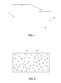
- Down-conversion represents a method for the generation of one or multiple electron ⁇ hole pairs, per incident high-energy photon, and can be used to reduce the thermalization losses. It is a material property that can be achieved if the material contains states or bands of intermediate energies. Incident high-energy photons can be transformed by the material into one or multiple lower energy photons. In a particular embodiment, the material is capable of emitting one photon per absorbed photon. FIG. 1 shows such energy levels of atoms in a down-converting material, and illustrates the process of down-conversion in which one photon of lower energy is produced. In some other embodiments, the material may emit more than one photon on absorption of one photon. As used herein "down-converting layer" may be a single layer, or may include multiple sub-layers.
- the down-converting layer comprises a phosphor material.
- such down-converting material contains a host material activated by a dopant (activator).
- a host material can be described as a transparent host lattice.
- a dopant adds desired energy levels at which incoming radiation is absorbed, such as an external photon, and a generated internal photon is preferentially emitted, based on the underlying absorber properties. Therefore, the down-converting material, at the basic level, contains an absorber and an emitter.
- dopant ions that may be used for 1 to 1 down-conversion include lanthanide ions, transition metal ions and rare-earth ions.
- suitable dopant ions include Ce 3+ , Eu 2+ , Sm 2+ , Cr 3+ , Mn 2+ and Mn 4+ .
- sensitizers may be doped into the host materials along with the dopants. Sensitizers are useful if the dopant ions cannot be excited, for example, because of forbidden transitions. The exciting energy is absorbed by the sensitizers and subsequently transferred to the dopant ions.
- transition metal ions may be sensitized by the lanthanide ions.
- FIG. 1 shows the emission of one photon as a result of absorption of a higher energy photon, it is possible to produce multiple photons per absorbed photon. In some embodiments, more than one photon is emitted per absorbed photon.
- This type of down-conversion is usually referred to as "quantum-cutting" or “quantum-splitting".
- a single dopant ion such as Pr 3+ , Tm 3+ or Gd 3+ , or a combination of two ions, such as the Gd 3+ -Eu 3+ dual ion, may be able to generate two low energy photons for every incident high-energy photon.
- Other combinations include Yb 3+ -Tb 3+ and Yb 3+ -Pr 3+ dual ions.
- Suitable examples of phosphor material may include halides, oxides and phosphates.
- Suitable examples of fluorides include, but are not limited to, samarium-doped BaAlF 5 , samarium-doped (Ba, Sr, Ca)MgF 4 .
- Non-limiting examples of other suitable phosphors may include samarium-doped strontium borate (SrB 4 O 7 :Sm 2+ ), samarium-doped (Sr, Ca, Ba)BPO 5 and europium-doped (Sr, Ca)SiO 4 .
- an organic down-converting material may include an organic dye, such as BASF LUMOGEN dye.
- a hybrid organic-inorganic dye may also be used for down-conversion.
- the down converting material comprises a quantum dot, such as a core-shell giant quantum dot system.
- the optical properties of the down-converting layer can be determined, in large part, by its material composition, particle size of down-converting material, thickness of the layer etc. By controlling the amount, particle size, and refractive index of the down-converting material, the refractive index and conversion properties of the down-converting layer may be tailored to minimize energy losses.
- the down-converting material may absorb radiation of a particular wavelength, or a particular range of wavelengths, while not scattering the radiation.
- the material may absorb radiation from UV, to visible, to near infrared, to infrared and converts the absorbed radiation to usable radiation.
- usable radiation refers to photons of a particular wavelength, or a particular range of wavelengths that takes part in energy conversion with high internal and external quantum efficiency. That is, the probability of collecting an electron-hole pair in that spectral range is high, usually greater than about 60%, and often greater than about 80%.
- the down-converting material emits such photons that can be absorbed by a semiconductor layer of the device to produce an electron-hole pair.
- the material absorbs radiation with wavelength below about 525 nm, and produces radiation with wavelength longer than 550 nm.
- the excitation and absorption properties of the down-converting layer, as well as the emission spectrum are designed to enhance external quantum efficiency (EQE) of the PV device.
- the material exhibits a refractive index value that should typically match well with refractive indices of adjacent mediums.
- This configuration advantageously provides reduced reflection at interfaces because of improved matching of refractive indices.
- the down-converting layer described herein benefits the photovoltaic device in two ways: (1) reduces absorption losses and (2) reduces reflection losses, and thus improves over all energy conversion.
- the down-converting layer may have a graded refractive index.
- the graded refractive index may be defined as a variation in the refractive index as a function of position in a selected direction, typically a direction perpendicular to a substrate supporting the layer.
- a value of refractive index at a first surface of the layer varies from a value of refractive index at a second surface of the layer.
- the variation in refractive index may be continuous in the selected direction or may occur in a series of discrete steps.
- the gradient of refractive index can be achieved by compositional variations.
- the graded composition provides a graded refractive index to the layer.
- the "graded composition" as defined herein refers to a gradual variation in the composition of the down-converting material in one direction, although the gradation may not always be constant. In this manner, the excitation and emission profile of the layer can be broadened, which will have beneficial effect of providing a broad coverage of wavelength ranges for the overall down-converting layer.
- the down-converting layer is a single layer.
- the down-converting layer includes more than one sub-layer. Multiple sub-layers of different refractive indices may be deposited, one over another, to attain the desired grading.
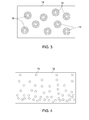
- the particles 10 of the down-converting material may be dispersed or embedded in a transparent matrix 12, as illustrated in FIG. 2 .
- the term "embedded” is used to indicate that the down-converting particles 10 are at least substantially enclosed within the matrix 12.
- the particles 10 are dispersed in such a manner that minimal agglomeration between the particles 10 is achieved.
- the refractive index of the matrix 12 may be higher than that of the down-converting material in some embodiments, and lower than that of the down-converting material in other embodiments.
- Such down-converting layer may also be referred to as “composite down-converting layer” and exhibit an "effective refractive index" which results from the combination of refraction due to particles and refraction due to the matrix (discussed in detail below).
- the effective refractive index of the composite down-converting layer depends on various parameters, such as refractive index of the matrix, refractive index of the down-converting material, and particle size of down-converting particles, among others.
- the refractive index of a medium is defined as the ratio of the velocity of light in a vacuum to that of the medium.
- Effective refractive index refers to refractive index of the composite down-converting layer having down-converting particles embedded in a matrix.
- the effective refractive index as defined herein, is used to determine the phase lag and attenuation of the coherent wave as electromagnetic radiation propagates through the layer.
- the parameters such as size, local volume fraction or area fraction, down-converting material fraction, matrix fraction and material refractive index, determine the effective refractive index of the layer.
- the refractive index of a material or medium may vary with wavelength. This effect is typically known as dispersion.
- the refractive indices of the down-converting material particles 10 and the matrix 12 may vary differently with wavelength.
- the dispersion of refractive indices for the down-converting particles 10 and the matrix 12 are chosen such that the refractive indices are well matched in the long wavelength range (> about 550 nanometers) of the solar spectrum so that scattering is minimized for incoming radiation in that range.
- the dispersion in the lower wavelength region specifically below about 525 nm, is chosen such that the refractive indices diverge such that photon-trapping in the composite layer can occur to improve absorption.
- the down-converting material may contain particles of various shapes and sizes depending on refractive index of the constituents' materials, difference in refractive indices ( ⁇ n) and scattering effects.
- the size of particles is in part, a function of ⁇ n.
- nanosize particles of the down-converting material are desirable, especially for ⁇ n larger than about 0.05.
- nanosize refers to average size of the down-converting particles in a range from about 1 nanometer to about 500 nanometers, and in some specific embodiments, from about 10 nanometers to about 100 nanometers. In some other instances, bigger particles may be used for ⁇ n less than about 0.05. In these instances, the average particle size ranges from about 0.5 micron to about 10 microns, and in specific embodiments, from about 1 micron to about 5 microns.
- the matrix 12 may include a non-conductive, non-crystalline material such as glass.
- glasses may include soda-lime glass, alumino-silicate glass, boro-silicate glass, silica, and low-iron glass.
- the matrix 12 may include a non-conductive crystalline material.
- Other suitable materials such as a dielectric material or a hybrid organic-inorganic material may also be used.
- the down-converting material particles 10 may be present in the matrix 12 in any amount (percentage) that is appropriate for the desired function.
- the down-converting particles 10 may be present at a level of between about 0.001 % to about 60 % by volume, depending on the type of the matrix material and type of down-converting material.
- the percentage (amount) may be in a range of from about 10 % to about 25 % by volume.
- the down-converting materials may also contain additional layers on them, for the purposes of surface passivation or improved refractive index matching (e.g. a core-shell structure).
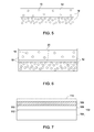
- FIG. 3 illustrates such an embodiment of core-shell structures 14 of down-converting particles 10 dispersed in the matrix 12.
- the particles 10 of down-converting material form the core, which are coated with one or more dielectric shell layers 16.
- the multiple shell layers 16 are configured such that they substantially match the refractive index of the matrix 12 on one side, and that of the phosphor particles 10 on the other.
- These shell layers 16 may allow for better optical coupling of incoming short wavelength radiation to the down-converting particles 10 so that scattering is reduced for the composite down-converting layer.
- the shell layers 16 may further allow for better out-coupling of down-converted long wavelength radiation into the matrix 12 of the composite layer.
- the down-converting particles 10 are coated with a thin layer of metal nanoparticles (not shown). These particles have strong plasmon resonance that helps to improve the emission efficiency (luminescent quantum efficiency) of down converted radiation from the down-converting particles 10.
- the metal nanoparticles are placed in direct contact with the down-converting particles 10, and in some other instances, the metal nanoparticles are separated by a thin dielectric shell that is first coated on the down-converting particles. The thickness of the shell layers may be about 1 nanometer to about 10 nanometers.
- These coated particles are then mixed with a liquid precursor matrix solution, which is deposited and solidified to form the composited down-converting layer.
- the down-converting particles 10 form a density gradient from a lower region to an upper region within the matrix 12. This density gradient provides gradation in refractive index of the layer in one direction, although the gradation may not always be constant.
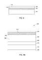
- the down-converting layer is a single layer having density gradation as illustrated in FIG. 4 .
- FIG. 5 illustrates another embodiment where the down-converting layer includes more than one sub-layer 18. Multiple sub-layers 18 of varying density of down-converting particles 10 may be deposited, one over another, to attain the desired refractive index grading. In some instances, sub-layers 18 of different refractive indices may be separated by dielectric layers 20 as illustrated in FIG. 6 .
- Suitable dielectric materials include silicon oxide, silicon nitride, titanium oxide, hafnium oxide or combinations thereof.
- the dielectric layers 20 may act as back reflectors that minimize reflectance of the photons emitted from the down-converting layer(s) back to a device.
- the down-converting layer has a thickness greater than about 100 nanometers.
- the thickness of the layer may be in a range of about 500 nanometers to about 1 micron.
- the thickness of each of the sub-layer may be in a range of about 500 nanometers to about 800 nanometers, in some instances.
- the down-converting layer has a thickness from about 1 micron to about 3000 microns, and in some specific embodiments from about 1 to about 100 microns.
- a down-converting layer characterized by a graded index profile provides good matching of refractive index at the interfaces resulting in less reflection than may be achieved with a uniform refractive index.
- the refractive index of the layer may increase or decrease with position from a first surface towards a second surface. Furthermore, the variation of the refractive index may also depend on the position of the layer in the device so that the values of refractive indices at the first and the second surface substantially match with the respective adjacent layers or mediums.
- the down-converting layer can be formed by a variety of techniques, such as physical vapor deposition, chemical deposition, sputtering, solution growth, and solution deposition. Other suitable techniques include dip-coating, spray-coating, spin-coating, slot-die coating, roller coating, gravure printing, ink-jet printing, screen printing, capillary printing, tape casting, flexo coating, extrusion coating, and combinations thereof.
- the down-converting layer may be disposed or attached to a variety of photovoltaic devices.
- the photovoltaic device includes a single junction or a multi-junction photovoltaic cell.
- Non-limiting examples of photovoltaic cells include an amorphous silicon cell, a crystalline silicon cell, a hybrid/heterojunction amorphous and crystalline silicon cell, a CdTe thin film cell, a micromorph tandem silicon thin film cell, a Cu(In,Ga,Al)(Se,S) 2 (also referred to as "CIGS") thin film cell, a copper-zinc-tin-sulfide (CZTS) thin film cell, a metal sulfide thin film cell, a metal phosphide thin film cell, a GaAs cell, a multiple-junction III-V-based solar cell, a dye-sensitized solar cell, or a solid-state organic/polymer solar cell.
- CZTS copper-zinc-tin
- FIG. 7 illustrates one embodiment of the present invention.
- a photovoltaic device 102 includes a photovoltaic cell 104 and a glass plate 106 on top of the cell 104.
- the down-converting layer 108 is disposed on a front side of the glass plate 106.
- the term "front side" of the glass plate 106 refers to a front surface 110 of the glass plate 106 that is exposed to ambient environment.
- the down-converting material for the layer 108 comprises a fluoride phosphor.
- a transparent dielectric layer 114 may be disposed over the down-converting layer 108 for the protection of the layer 108, in some embodiments.
- the down-converting layer 108 may be disposed on a rear side of the glass plate 106 as illustrated in FIG. 8 .
- the down-converting layer 108 comprises an oxide phosphor.
- the glass plate 106 may have a substantially planar surface.
- a "substantially planar surface”, as defined herein, usually refers to a substantially flat surface.
- the surface can be smooth, although it may include a relatively minor degree (e.g., an RMS roughness that is less than about 1 micron, or more specifically less than about 300 nm) of texture, indentations, and various irregularities. These irregularities, textures, or patterns, may be useful in minimizing light trapping in the down-converting layer and channeling the converted radiation to the device by refraction at the dimpled surface.
- FIG. 9A , 9B, and 9C illustrate examples of embodiments of a thin-film heterojunction PV device 200, such as a CdTe PV device or a Cu(In,Ga)Se 2 (CIGS) PV device.
- the device 200 includes a glass plate 202 having a first surface 204 and a second surface 206.
- the glass plate 202 acts as a substrate, in certain instances, for example in the case of a CdTe PV device.
- the glass plate 202 acts as a cover and the device 200 further includes a substrate 222.
- Substrate selection in these instances, may include substrates of any suitable material, including, but not limited to, metal, semiconductor, doped semiconductor, amorphous dielectrics, crystalline dielectrics, and combinations thereof.
- a transparent conductive layer 208 is disposed on the first surface 204 of the glass plate.
- Suitable materials for transparent conductive layer 106 may include an oxide, sulfide, phosphide, telluride, or combinations thereof. These transparent conductive materials may be doped or undoped.
- the conductive oxide may include zinc oxide, tin oxide, aluminum doped zinc oxide, fluorine-doped tin oxide, cadmium stannate (cadmium tin oxide), or zinc stannate (zinc tin oxide).
- the conductive oxide includes indium-containing oxides.
- suitable indium containing oxides are indium tin oxide (ITO), Ga-In-Sn-O, Zn-In-Sn-O, Ga-In-O, Zn-In-O, and combinations thereof.
- Suitable sulfides may include cadmium sulfide, indium sulfide and the like.
- Suitable phosphides may include indium phosphide, gallium phosphide, and the like.
- a first type semiconductor layer 210 is disposed on the transparent conductive layer 208 and a second type semiconductor layer 212 is disposed on the first type semiconductor layer 210.
- the first type semiconductor layer 210 and the second type semiconductor layer 212 may be doped with a p-type doping or n-type doping such as to form a heterojunction.
- a heterojunction is a semiconductor junction, which is composed of layers of dissimilar semiconductor material. These materials usually have non-equal band gaps.
- a heterojunction can be formed by contact between a layer or region of one conductivity type with a layer or region of opposite conductivity, e.g., a "p-n" junction.
- other devices which utilize the heterojunction, include thin film transistors and bipolar transistors.
- the second type semiconductor material layer 212 includes an absorber layer.
- the absorber layer is a part of a photovoltaic device where the conversion of electromagnetic energy of incident light (for instance, sunlight) to electron-hole pairs (that is, to electrical current), occurs.
- a photo-active material is typically used for forming the absorber layer.
- the second type semiconductor material used for the absorber layer includes Cu(In,Ga,Al)(Se,S) 2 (also referred to as "CIGS"). In some instances, CIGS may further be substituted with an additional element, for example silver.
- CIGS layer or film may be manufactured by various known methods.
- Examples of such methods include vacuum-based processes, which co-evaporate, or co-sputter copper, gallium and indium, reactive sputtering, ion beam deposition, solution based deposition of nanoparticles precursors, and metal-organic chemical vapor deposition.
- Cadmium telluride is another photo-active material, which may be used for the absorber layer, in one embodiment.
- CdTe is an efficient photo-active material that is used in thin-film photovoltaic devices.
- CdTe is relatively easy to deposit and therefore is considered suitable for large-scale production.
- a typical method to deposit CdTe is closed-space sublimation.
- CdTe PV devices photovoltaic devices including CdTe as the photo-active material
- CIGS PV devices those including CIGS
- An example of the first type semiconductor 210 includes cadmium sulfide (CdS).
- Cadmium sulfide absorbs radiation strongly at wavelengths below about 500 nanometers and significantly reduces the quantum efficiency of a device in this wavelength region.
- a down-converting layer 214 is disposed on the device in front of the cadmium sulfide layer 210 that may absorb radiation with wavelength lower than about 525 nanometers and convert them to longer wavelengths, in these instances.
- the down-converting layer 214 may be disposed on the second surface 206 of the glass plate 202 that is exposed to ambient as shown in FIG 9A .
- the layer 214 may optionally be coated with a thin dielectric layer 216.
- the dielectric layer 216 may include a back reflector that minimizes reflectance and assists in redirecting emitted radiation to the PV device.
- the back reflector as used herein, is a substantially transparent layer and has a dielectric constant that is equal to or less than the dielectric constant of a down-converting layer. Suitable dielectric materials include silicon oxide, silicon nitride, titanium oxide, hafnium oxide, and combinations thereof.
- the down-converting particles 220 are dispersed within the glass plate as illustrated in FIG. 9B .
- the down-converting layer 214 is disposed adjacent to the transparent conductive oxide layer, i.e. between the glass plate 202 and the transparent conducting layer 208.
- a thin dielectric layer 218 optionally may be disposed between the first surface 204 of the glass plate 202 and down-converting layer 214. This dielectric layer 218 acts as a diffusion barrier for ions to enter the down-converting layer 214 and the PV cell from the glass plate 202.
- the above-mentioned photo-active semiconductor materials may be used alone or in combination. Also, these materials may be present in more than one layer, each layer having different type of photo-active material or having combinations of the materials in separate layers.
- One of the ordinary skills in the art would be able to optimally configure the construction and the amount of the photo-active materials to maximize the efficiency of the photovoltaic cell.
- the photovoltaic module may have an array of a number of the photovoltaic devices described above electrically connected in series or in parallel. Substantially all photovoltaic devices include down-converting layer disposed on the device as discussed in above embodiments. In some instances, the down-converting layer may be disposed on entire photovoltaic module. In some other embodiments, edges of the module are painted with a diffuse reflecting paint to reduce reflection and escape of emitted photon from the edge of the module.
- Phosphor particles were formed by high temperature reaction process, followed by mechanical ball milling. Milling was continued for the time required to achieve desired particle size. These particles of desired amount were dispersed in a liquid glass precursor solution by mixing them ultrasonically.
- Phosphor particle of desired size are prepared as described in method I. Prior to incorporation in the liquid glass precursor solution, the particles are subject to TEOS- based chemistry in chemical baths for deposition of various transparent oxide layer on the particle surface. These shell layers provide a graded index on the particle surface that is more effectively allow light to enter the particles for down-conversion.
- BaAlF 5 :Sm 2+ particle were formed by using method I.
- the mean particle size of the phosphor particles is about 2 microns, and the refractive index for both particles and matrix is ⁇ 1.43 with a difference of less than 0.04. These particles were dispersed in a liquid glass precursor solution. The amount of particles in the precursor solution was about 33 weight percent.
- a CdTe PV module was fabricated using a standard manufacturing process on a glass substrate.
- the liquid glass precursor solution containing BaAlF 5 : Sm 2+ particle was applied to an outer surface of the glass by using both spin coating and spray coating techniques.
- the layer was then annealed at a temperature of about 80°C to form a solid glass matrix containing the BaAlF 5 :Sm 2+ particle (composite down-converting layer).
- the thickness of this layer was about 3 microns.
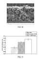
- a micrograph of such a layer is shown in FIG 10 .
- the composite layer had an effective refractive index of about 1.43 between the refractive indices of air and the underlying glass substrate.
- FIG. 11 shows improved efficiency of the CdTe PV module as compared to a CdTe PV module without such composite layer.
- the CdTe PV module having the composite down-converting layer showed an increased efficiency by 0.2 percent absolute.
- SrB 4 O 7 :Sm 2+ particles are formed by high temperature reaction process, followed by mechanical ball milling. Milling is continued until particles of average size less than about 100 nm are achieved. These particles are dispersed in a liquid glass precursor solution. The difference in refractive indices of the oxide particles and the glass is more than about 0.05 (- 1.7). Three different solutions are prepared with about 30 weight percent, about 20 weight percent, and about 10 weight percent of particles in the precursor solution.
- a CdTe PV module is fabricated using a standard manufacturing process. At the end of manufacturing, the solution containing the highest weight percent of particles is deposited on a glass substrate first, followed by a solution with the second high loading, and then a solution with the lowest loading to attain graded refractive index.
- the layers are applied using roller techniques.
- the layers are then annealed at a temperature of about 80°C to form a solid glass matrix containing the SrB 4 O 7 :Sm 2+ particles (composite down-converting layers).
- the composite layers have an effective refractive index that is decreasing respectively for about 30 weight percent, about 20 weight percent, and about 10 weight percent of particles in the precursor solution.
Landscapes
- Chemical & Material Sciences (AREA)
- Engineering & Computer Science (AREA)
- Materials Engineering (AREA)
- Organic Chemistry (AREA)
- Inorganic Chemistry (AREA)
- Condensed Matter Physics & Semiconductors (AREA)
- Physics & Mathematics (AREA)
- Electromagnetism (AREA)
- General Physics & Mathematics (AREA)
- Computer Hardware Design (AREA)
- Microelectronics & Electronic Packaging (AREA)
- Power Engineering (AREA)
- Photovoltaic Devices (AREA)
Applications Claiming Priority (1)
| Application Number | Priority Date | Filing Date | Title |
|---|---|---|---|
| US12/894,916 US20120080066A1 (en) | 2010-09-30 | 2010-09-30 | Photovoltaic devices |
Publications (2)
| Publication Number | Publication Date |
|---|---|
| EP2437314A2 true EP2437314A2 (fr) | 2012-04-04 |
| EP2437314A3 EP2437314A3 (fr) | 2013-05-22 |
Family
ID=44719433
Family Applications (1)
| Application Number | Title | Priority Date | Filing Date |
|---|---|---|---|
| EP11182365.4A Withdrawn EP2437314A3 (fr) | 2010-09-30 | 2011-09-22 | Dispositifs photovoltaïques |
Country Status (4)
| Country | Link |
|---|---|
| US (1) | US20120080066A1 (fr) |
| EP (1) | EP2437314A3 (fr) |
| CN (1) | CN102446987A (fr) |
| AU (1) | AU2011226901A1 (fr) |
Families Citing this family (6)
| Publication number | Priority date | Publication date | Assignee | Title |
|---|---|---|---|---|
| US8415759B2 (en) * | 2010-11-23 | 2013-04-09 | Raytheon Company | Down-converting and detecting photons |
| KR101193172B1 (ko) * | 2011-02-22 | 2012-10-19 | 삼성에스디아이 주식회사 | 염료 감응 태양전지 |
| US9091748B2 (en) | 2012-04-18 | 2015-07-28 | Raytheon Company | Methods and apparatus for 3D UV imaging |
| WO2014120342A2 (fr) * | 2012-12-14 | 2014-08-07 | Raydex Technology, Inc. | Couche antireflet à large bande destinée à des dispositifs photovoltaïques et à d'autres dispositifs |
| CN106410031B (zh) * | 2016-03-29 | 2020-01-17 | 上海大学 | 入射光强度可调的有机太阳能电池及其制备方法 |
| NL2021109B1 (en) * | 2018-06-12 | 2019-12-17 | Physee Group B V | Inorganic luminescent materials for solar radiation conversion devices |
Family Cites Families (17)
| Publication number | Priority date | Publication date | Assignee | Title |
|---|---|---|---|---|
| DE2926191A1 (de) * | 1978-07-04 | 1980-01-17 | Yissum Res Dev Co | Sonnenkollektor |
| US7204630B2 (en) * | 2004-06-30 | 2007-04-17 | 3M Innovative Properties Company | Phosphor based illumination system having a plurality of light guides and an interference reflector |
| WO2008051235A2 (fr) * | 2005-11-10 | 2008-05-02 | The Board Of Trustees Of The University Of Illinois | Dispositifs photovoltaïques à nanoparticules de silicium |
| WO2007114871A2 (fr) * | 2005-12-22 | 2007-10-11 | Solbeam, Inc. | Ensembles de prisme électro-optique |
| KR100746749B1 (ko) * | 2006-03-15 | 2007-08-09 | (주)케이디티 | 광 여기 시트 |
| TWI401809B (zh) * | 2006-03-31 | 2013-07-11 | Intematix Corp | 具有增強之轉換效率之光伏打裝置及波長轉換器及其方法 |
| US20070295383A1 (en) * | 2006-03-31 | 2007-12-27 | Intematix Corporation | Wavelength-converting phosphors for enhancing the efficiency of a photovoltaic device |
| US8197720B2 (en) * | 2007-01-22 | 2012-06-12 | Konica Minolta Medical & Graphic, Inc. | Core/shell type semiconductor nanoparticle and method for production thereof |
| US8039736B2 (en) * | 2008-08-18 | 2011-10-18 | Andrew Clark | Photovoltaic up conversion and down conversion using rare earths |
| WO2009046060A2 (fr) * | 2007-10-01 | 2009-04-09 | Davis, Joseph And Negley | Appareils et procédés pour produire de l'énergie électrique renforcée de photons par conversion-abaissement |
| DE102007049029A1 (de) * | 2007-10-11 | 2009-04-23 | Bundesrepublik Deutschland, vertr. durch d. Bundesministerium f. Wirtschaft und Technologie, dieses vertreten durch d. Präsidenten d. Physikalisch-Technischen Bundesanstalt | Konversionsschicht, Detektor, Detektoranordnung und Verfahren zum Herstellen von Konversionsschichten |
| US8664513B2 (en) * | 2007-10-12 | 2014-03-04 | OmniPV, Inc. | Solar modules with enhanced efficiencies via use of spectral concentrators |
| TWI390008B (zh) * | 2007-12-12 | 2013-03-21 | Solar cells and their light-emitting conversion layer | |
| US20090255577A1 (en) * | 2008-04-04 | 2009-10-15 | Michael Tischler | Conversion Solar Cell |
| WO2009148131A1 (fr) * | 2008-06-06 | 2009-12-10 | 住友ベークライト株式会社 | Composition de conversion de longueur d'onde et dispositif photovoltaïque comportant une couche composée de la composition de conversion de longueur d'onde |
| JP2010034502A (ja) * | 2008-06-30 | 2010-02-12 | Hitachi Chem Co Ltd | 波長変換フィルム、これを用いた太陽電池モジュール及びこれらの製造方法 |
| TW201005972A (en) * | 2008-07-17 | 2010-02-01 | Nexpower Technology Corp | Thin film solar cell having photo-luminescent medium coated therein and manufacturing method thereof |
-
2010
- 2010-09-30 US US12/894,916 patent/US20120080066A1/en not_active Abandoned
-
2011
- 2011-09-22 EP EP11182365.4A patent/EP2437314A3/fr not_active Withdrawn
- 2011-09-27 AU AU2011226901A patent/AU2011226901A1/en not_active Abandoned
- 2011-09-29 CN CN2011103093127A patent/CN102446987A/zh active Pending
Non-Patent Citations (1)
| Title |
|---|
| None |
Also Published As
| Publication number | Publication date |
|---|---|
| AU2011226901A1 (en) | 2012-04-19 |
| US20120080066A1 (en) | 2012-04-05 |
| EP2437314A3 (fr) | 2013-05-22 |
| CN102446987A (zh) | 2012-05-09 |
Similar Documents
| Publication | Publication Date | Title |
|---|---|---|
| EP2437315A2 (fr) | Dispositifs photovoltaïques | |
| AU2010202874B2 (en) | Nanostructured functional coatings and devices | |
| EP2437314A2 (fr) | Dispositifs photovoltaïques | |
| KR101575733B1 (ko) | 근적외선 파장변환 구조체 및 이를 이용한 태양전지 | |
| MX2013015438A (es) | Un panel espectralmente selectivo. | |
| EP2437313A2 (fr) | Dispositifs photovoltaïques | |
| US20240006546A1 (en) | Tandem photovoltaic device | |
| JP3837114B2 (ja) | 太陽電池 | |
| CN102013440A (zh) | 薄膜太阳能组件及制造方法 | |
| KR20210099964A (ko) | 양면 수광형 태양전지의 제조방법 및 이를 통해 제조한 양면 수광형 태양전지 | |
| JP2005347444A (ja) | 光起電力素子 | |
| JP2011151068A (ja) | 光電変換装置 | |
| US20130247994A1 (en) | Photovoltaic device | |
| JP5469298B2 (ja) | 光電変換装置用透明導電膜、及びその製造方法 | |
| JP5144949B2 (ja) | 薄膜光電変換装置用基板とそれを含む薄膜光電変換装置の製造方法 | |
| KR101404243B1 (ko) | 형광체를 포함하는 태양전지 및 이의 제조방법 | |
| KR20110077923A (ko) | 박막 태양전지의 전면 전극 및 그를 포함하는 박막 실리콘 태양전지 | |
| EP4404280A1 (fr) | Photopile | |
| Abdulkadir | Fabrication And Characterization Of Black Silicon For Heterojunction Solar Cells | |
| KR101306450B1 (ko) | 태양전지 모듈 및 이의 제조방법 | |
| CN114163138B (zh) | 一种光谱转换纳米棒阵列的制备方法 | |
| WO2024176803A1 (fr) | Film électroconducteur transparent, substrat possédant un film électroconducteur transparent et élément de conversion photoélectrique | |
| KR101404353B1 (ko) | 형광체를 포함하는 태양전지 및 이의 제조방법 | |
| Chiu et al. | Enhancing performance of planar thin-film silicon solar cell using TiO2 ARC and luminescent down-shifting layers | |
| KR101173402B1 (ko) | 태양전지 및 이의 제조방법 |
Legal Events
| Date | Code | Title | Description |
|---|---|---|---|
| PUAI | Public reference made under article 153(3) epc to a published international application that has entered the european phase |
Free format text: ORIGINAL CODE: 0009012 |
|
| AK | Designated contracting states |
Kind code of ref document: A2 Designated state(s): AL AT BE BG CH CY CZ DE DK EE ES FI FR GB GR HR HU IE IS IT LI LT LU LV MC MK MT NL NO PL PT RO RS SE SI SK SM TR |
|
| AX | Request for extension of the european patent |
Extension state: BA ME |
|
| PUAL | Search report despatched |
Free format text: ORIGINAL CODE: 0009013 |
|
| AK | Designated contracting states |
Kind code of ref document: A3 Designated state(s): AL AT BE BG CH CY CZ DE DK EE ES FI FR GB GR HR HU IE IS IT LI LT LU LV MC MK MT NL NO PL PT RO RS SE SI SK SM TR |
|
| AX | Request for extension of the european patent |
Extension state: BA ME |
|
| RIC1 | Information provided on ipc code assigned before grant |
Ipc: H01L 31/055 20060101AFI20130418BHEP |
|
| 17P | Request for examination filed |
Effective date: 20131121 |
|
| RBV | Designated contracting states (corrected) |
Designated state(s): AL AT BE BG CH CY CZ DE DK EE ES FI FR GB GR HR HU IE IS IT LI LT LU LV MC MK MT NL NO PL PT RO RS SE SI SK SM TR |
|
| RAP1 | Party data changed (applicant data changed or rights of an application transferred) |
Owner name: FIRST SOLAR MALAYSIA SDN.BHD |
|
| 17Q | First examination report despatched |
Effective date: 20150306 |
|
| STAA | Information on the status of an ep patent application or granted ep patent |
Free format text: STATUS: EXAMINATION IS IN PROGRESS |
|
| STAA | Information on the status of an ep patent application or granted ep patent |
Free format text: STATUS: THE APPLICATION IS DEEMED TO BE WITHDRAWN |
|
| 18D | Application deemed to be withdrawn |
Effective date: 20180404 |