EP2437313A2 - Photovoltaische Vorrichtungen - Google Patents
Photovoltaische Vorrichtungen Download PDFInfo
- Publication number
- EP2437313A2 EP2437313A2 EP11182364A EP11182364A EP2437313A2 EP 2437313 A2 EP2437313 A2 EP 2437313A2 EP 11182364 A EP11182364 A EP 11182364A EP 11182364 A EP11182364 A EP 11182364A EP 2437313 A2 EP2437313 A2 EP 2437313A2
- Authority
- EP
- European Patent Office
- Prior art keywords
- layer
- converting
- photovoltaic device
- type semiconductor
- glass plate
- Prior art date
- Legal status (The legal status is an assumption and is not a legal conclusion. Google has not performed a legal analysis and makes no representation as to the accuracy of the status listed.)
- Withdrawn
Links
- 239000011521 glass Substances 0.000 claims abstract description 42
- 239000004065 semiconductor Substances 0.000 claims abstract description 37
- 230000005855 radiation Effects 0.000 claims abstract description 24
- 239000000463 material Substances 0.000 claims description 60
- 239000002245 particle Substances 0.000 claims description 55
- 239000011159 matrix material Substances 0.000 claims description 25
- MARUHZGHZWCEQU-UHFFFAOYSA-N 5-phenyl-2h-tetrazole Chemical compound C1=CC=CC=C1C1=NNN=N1 MARUHZGHZWCEQU-UHFFFAOYSA-N 0.000 claims description 16
- 239000000758 substrate Substances 0.000 claims description 12
- OAICVXFJPJFONN-UHFFFAOYSA-N Phosphorus Chemical compound [P] OAICVXFJPJFONN-UHFFFAOYSA-N 0.000 claims description 11
- WUPHOULIZUERAE-UHFFFAOYSA-N 3-(oxolan-2-yl)propanoic acid Chemical compound OC(=O)CCC1CCCO1 WUPHOULIZUERAE-UHFFFAOYSA-N 0.000 claims description 8
- 229910052980 cadmium sulfide Inorganic materials 0.000 claims description 8
- 239000003989 dielectric material Substances 0.000 claims description 7
- 229910052712 strontium Inorganic materials 0.000 claims description 6
- 150000004820 halides Chemical class 0.000 claims description 4
- 229910019142 PO4 Inorganic materials 0.000 claims description 3
- WILFBXOGIULNAF-UHFFFAOYSA-N copper sulfanylidenetin zinc Chemical compound [Sn]=S.[Zn].[Cu] WILFBXOGIULNAF-UHFFFAOYSA-N 0.000 claims description 3
- 229910052909 inorganic silicate Inorganic materials 0.000 claims description 3
- 239000011368 organic material Substances 0.000 claims description 3
- LNSYCBFBTCINRL-UHFFFAOYSA-N tristrontium;diborate Chemical compound [Sr+2].[Sr+2].[Sr+2].[O-]B([O-])[O-].[O-]B([O-])[O-] LNSYCBFBTCINRL-UHFFFAOYSA-N 0.000 claims description 3
- NBIIXXVUZAFLBC-UHFFFAOYSA-K phosphate Chemical compound [O-]P([O-])([O-])=O NBIIXXVUZAFLBC-UHFFFAOYSA-K 0.000 claims description 2
- 239000010452 phosphate Substances 0.000 claims description 2
- 230000001681 protective effect Effects 0.000 claims description 2
- 239000010410 layer Substances 0.000 description 167
- 238000006243 chemical reaction Methods 0.000 description 20
- 238000000034 method Methods 0.000 description 14
- 238000010521 absorption reaction Methods 0.000 description 13
- 239000002131 composite material Substances 0.000 description 11
- 150000002500 ions Chemical class 0.000 description 10
- 239000002019 doping agent Substances 0.000 description 9
- 239000006096 absorbing agent Substances 0.000 description 8
- 239000010409 thin film Substances 0.000 description 8
- 239000011149 active material Substances 0.000 description 7
- 230000006870 function Effects 0.000 description 6
- -1 rare-earth ions Chemical class 0.000 description 6
- 239000002243 precursor Substances 0.000 description 5
- VYPSYNLAJGMNEJ-UHFFFAOYSA-N Silicium dioxide Chemical compound O=[Si]=O VYPSYNLAJGMNEJ-UHFFFAOYSA-N 0.000 description 4
- XLOMVQKBTHCTTD-UHFFFAOYSA-N Zinc monoxide Chemical compound [Zn]=O XLOMVQKBTHCTTD-UHFFFAOYSA-N 0.000 description 4
- 238000000151 deposition Methods 0.000 description 4
- 239000000203 mixture Substances 0.000 description 4
- 230000003287 optical effect Effects 0.000 description 4
- GWEVSGVZZGPLCZ-UHFFFAOYSA-N Titan oxide Chemical compound O=[Ti]=O GWEVSGVZZGPLCZ-UHFFFAOYSA-N 0.000 description 3
- 229910052782 aluminium Inorganic materials 0.000 description 3
- 239000010949 copper Substances 0.000 description 3
- 230000008021 deposition Effects 0.000 description 3
- 239000006185 dispersion Substances 0.000 description 3
- 229910052733 gallium Inorganic materials 0.000 description 3
- 229910052738 indium Inorganic materials 0.000 description 3
- APFVFJFRJDLVQX-UHFFFAOYSA-N indium atom Chemical compound [In] APFVFJFRJDLVQX-UHFFFAOYSA-N 0.000 description 3
- 230000007246 mechanism Effects 0.000 description 3
- 239000002082 metal nanoparticle Substances 0.000 description 3
- 239000002356 single layer Substances 0.000 description 3
- 229910020923 Sn-O Inorganic materials 0.000 description 2
- 230000008901 benefit Effects 0.000 description 2
- 229910019990 cerium-doped yttrium aluminum garnet Inorganic materials 0.000 description 2
- 239000011258 core-shell material Substances 0.000 description 2
- 238000010168 coupling process Methods 0.000 description 2
- 238000005859 coupling reaction Methods 0.000 description 2
- 239000002178 crystalline material Substances 0.000 description 2
- 230000009977 dual effect Effects 0.000 description 2
- 230000000694 effects Effects 0.000 description 2
- 230000005670 electromagnetic radiation Effects 0.000 description 2
- 230000005284 excitation Effects 0.000 description 2
- AMGQUBHHOARCQH-UHFFFAOYSA-N indium;oxotin Chemical compound [In].[Sn]=O AMGQUBHHOARCQH-UHFFFAOYSA-N 0.000 description 2
- 229910021644 lanthanide ion Inorganic materials 0.000 description 2
- 238000011068 loading method Methods 0.000 description 2
- 229910052751 metal Inorganic materials 0.000 description 2
- 239000002184 metal Substances 0.000 description 2
- 230000003071 parasitic effect Effects 0.000 description 2
- 235000021317 phosphate Nutrition 0.000 description 2
- 235000019353 potassium silicate Nutrition 0.000 description 2
- 230000008569 process Effects 0.000 description 2
- 239000002096 quantum dot Substances 0.000 description 2
- 229910052814 silicon oxide Inorganic materials 0.000 description 2
- 230000003595 spectral effect Effects 0.000 description 2
- XOLBLPGZBRYERU-UHFFFAOYSA-N tin dioxide Chemical compound O=[Sn]=O XOLBLPGZBRYERU-UHFFFAOYSA-N 0.000 description 2
- 229910001887 tin oxide Inorganic materials 0.000 description 2
- 229910001428 transition metal ion Inorganic materials 0.000 description 2
- 239000011787 zinc oxide Substances 0.000 description 2
- RYGMFSIKBFXOCR-UHFFFAOYSA-N Copper Chemical compound [Cu] RYGMFSIKBFXOCR-UHFFFAOYSA-N 0.000 description 1
- 229910005540 GaP Inorganic materials 0.000 description 1
- GYHNNYVSQQEPJS-UHFFFAOYSA-N Gallium Chemical compound [Ga] GYHNNYVSQQEPJS-UHFFFAOYSA-N 0.000 description 1
- GPXJNWSHGFTCBW-UHFFFAOYSA-N Indium phosphide Chemical compound [In]#P GPXJNWSHGFTCBW-UHFFFAOYSA-N 0.000 description 1
- 229910052581 Si3N4 Inorganic materials 0.000 description 1
- XUIMIQQOPSSXEZ-UHFFFAOYSA-N Silicon Chemical compound [Si] XUIMIQQOPSSXEZ-UHFFFAOYSA-N 0.000 description 1
- UCKMPCXJQFINFW-UHFFFAOYSA-N Sulphide Chemical compound [S-2] UCKMPCXJQFINFW-UHFFFAOYSA-N 0.000 description 1
- 229910007611 Zn—In—O Inorganic materials 0.000 description 1
- 239000012190 activator Substances 0.000 description 1
- 238000005054 agglomeration Methods 0.000 description 1
- 230000002776 aggregation Effects 0.000 description 1
- XAGFODPZIPBFFR-UHFFFAOYSA-N aluminium Chemical compound [Al] XAGFODPZIPBFFR-UHFFFAOYSA-N 0.000 description 1
- 239000005354 aluminosilicate glass Substances 0.000 description 1
- 238000000498 ball milling Methods 0.000 description 1
- 230000004888 barrier function Effects 0.000 description 1
- 230000009286 beneficial effect Effects 0.000 description 1
- 230000008033 biological extinction Effects 0.000 description 1
- 230000005540 biological transmission Effects 0.000 description 1
- 239000005388 borosilicate glass Substances 0.000 description 1
- 229910052793 cadmium Inorganic materials 0.000 description 1
- BEQNOZDXPONEMR-UHFFFAOYSA-N cadmium;oxotin Chemical compound [Cd].[Sn]=O BEQNOZDXPONEMR-UHFFFAOYSA-N 0.000 description 1
- 239000000969 carrier Substances 0.000 description 1
- 230000008859 change Effects 0.000 description 1
- 230000005465 channeling Effects 0.000 description 1
- 239000002800 charge carrier Substances 0.000 description 1
- 238000005234 chemical deposition Methods 0.000 description 1
- 238000005229 chemical vapour deposition Methods 0.000 description 1
- 239000011248 coating agent Substances 0.000 description 1
- 238000000576 coating method Methods 0.000 description 1
- 230000001427 coherent effect Effects 0.000 description 1
- 239000004020 conductor Substances 0.000 description 1
- 239000000470 constituent Substances 0.000 description 1
- 238000010276 construction Methods 0.000 description 1
- 229910052802 copper Inorganic materials 0.000 description 1
- 230000008878 coupling Effects 0.000 description 1
- 239000013078 crystal Substances 0.000 description 1
- 238000005520 cutting process Methods 0.000 description 1
- 230000003247 decreasing effect Effects 0.000 description 1
- 230000001419 dependent effect Effects 0.000 description 1
- 238000010586 diagram Methods 0.000 description 1
- 238000009792 diffusion process Methods 0.000 description 1
- 238000003618 dip coating Methods 0.000 description 1
- 238000000295 emission spectrum Methods 0.000 description 1
- 238000007765 extrusion coating Methods 0.000 description 1
- 239000010408 film Substances 0.000 description 1
- 238000007775 flexo coating Methods 0.000 description 1
- 150000002222 fluorine compounds Chemical class 0.000 description 1
- HZXMRANICFIONG-UHFFFAOYSA-N gallium phosphide Chemical compound [Ga]#P HZXMRANICFIONG-UHFFFAOYSA-N 0.000 description 1
- 238000007646 gravure printing Methods 0.000 description 1
- 229910000449 hafnium oxide Inorganic materials 0.000 description 1
- WIHZLLGSGQNAGK-UHFFFAOYSA-N hafnium(4+);oxygen(2-) Chemical compound [O-2].[O-2].[Hf+4] WIHZLLGSGQNAGK-UHFFFAOYSA-N 0.000 description 1
- 230000006872 improvement Effects 0.000 description 1
- 238000010348 incorporation Methods 0.000 description 1
- 238000007373 indentation Methods 0.000 description 1
- 238000007641 inkjet printing Methods 0.000 description 1
- 229910010272 inorganic material Inorganic materials 0.000 description 1
- 239000011147 inorganic material Substances 0.000 description 1
- 238000007737 ion beam deposition Methods 0.000 description 1
- XEEYBQQBJWHFJM-UHFFFAOYSA-N iron Substances [Fe] XEEYBQQBJWHFJM-UHFFFAOYSA-N 0.000 description 1
- 229910052742 iron Inorganic materials 0.000 description 1
- 238000011031 large-scale manufacturing process Methods 0.000 description 1
- 239000012705 liquid precursor Substances 0.000 description 1
- 229910052976 metal sulfide Inorganic materials 0.000 description 1
- 238000003801 milling Methods 0.000 description 1
- 238000002156 mixing Methods 0.000 description 1
- 239000002105 nanoparticle Substances 0.000 description 1
- 230000005693 optoelectronics Effects 0.000 description 1
- KYKLWYKWCAYAJY-UHFFFAOYSA-N oxotin;zinc Chemical compound [Zn].[Sn]=O KYKLWYKWCAYAJY-UHFFFAOYSA-N 0.000 description 1
- 239000003973 paint Substances 0.000 description 1
- 238000002161 passivation Methods 0.000 description 1
- 150000003013 phosphoric acid derivatives Chemical class 0.000 description 1
- 238000005240 physical vapour deposition Methods 0.000 description 1
- 238000002360 preparation method Methods 0.000 description 1
- 238000007639 printing Methods 0.000 description 1
- 238000001552 radio frequency sputter deposition Methods 0.000 description 1
- 229910052761 rare earth metal Inorganic materials 0.000 description 1
- 238000005546 reactive sputtering Methods 0.000 description 1
- 238000011160 research Methods 0.000 description 1
- 238000007761 roller coating Methods 0.000 description 1
- 238000007650 screen-printing Methods 0.000 description 1
- 229910052710 silicon Inorganic materials 0.000 description 1
- 239000010703 silicon Substances 0.000 description 1
- 239000000377 silicon dioxide Substances 0.000 description 1
- HQVNEWCFYHHQES-UHFFFAOYSA-N silicon nitride Chemical compound N12[Si]34N5[Si]62N3[Si]51N64 HQVNEWCFYHHQES-UHFFFAOYSA-N 0.000 description 1
- 229910052709 silver Inorganic materials 0.000 description 1
- 239000004332 silver Substances 0.000 description 1
- 238000007764 slot die coating Methods 0.000 description 1
- 239000005361 soda-lime glass Substances 0.000 description 1
- 238000001228 spectrum Methods 0.000 description 1
- 238000004528 spin coating Methods 0.000 description 1
- 238000005507 spraying Methods 0.000 description 1
- 238000004544 sputter deposition Methods 0.000 description 1
- 229940071182 stannate Drugs 0.000 description 1
- 238000000859 sublimation Methods 0.000 description 1
- 230000008022 sublimation Effects 0.000 description 1
- 239000000126 substance Substances 0.000 description 1
- GKCNVZWZCYIBPR-UHFFFAOYSA-N sulfanylideneindium Chemical compound [In]=S GKCNVZWZCYIBPR-UHFFFAOYSA-N 0.000 description 1
- 150000004763 sulfides Chemical class 0.000 description 1
- 238000010345 tape casting Methods 0.000 description 1
- XSOKHXFFCGXDJZ-UHFFFAOYSA-N telluride(2-) Chemical compound [Te-2] XSOKHXFFCGXDJZ-UHFFFAOYSA-N 0.000 description 1
- 239000004408 titanium dioxide Substances 0.000 description 1
- OGIDPMRJRNCKJF-UHFFFAOYSA-N titanium oxide Inorganic materials [Ti]=O OGIDPMRJRNCKJF-UHFFFAOYSA-N 0.000 description 1
- 238000012546 transfer Methods 0.000 description 1
- 230000007704 transition Effects 0.000 description 1
- BNEMLSQAJOPTGK-UHFFFAOYSA-N zinc;dioxido(oxo)tin Chemical compound [Zn+2].[O-][Sn]([O-])=O BNEMLSQAJOPTGK-UHFFFAOYSA-N 0.000 description 1
Images

Classifications
-
- H—ELECTRICITY
- H10—SEMICONDUCTOR DEVICES; ELECTRIC SOLID-STATE DEVICES NOT OTHERWISE PROVIDED FOR
- H10F—INORGANIC SEMICONDUCTOR DEVICES SENSITIVE TO INFRARED RADIATION, LIGHT, ELECTROMAGNETIC RADIATION OF SHORTER WAVELENGTH OR CORPUSCULAR RADIATION
- H10F77/00—Constructional details of devices covered by this subclass
- H10F77/40—Optical elements or arrangements
- H10F77/42—Optical elements or arrangements directly associated or integrated with photovoltaic cells, e.g. light-reflecting means or light-concentrating means
- H10F77/45—Wavelength conversion means, e.g. by using luminescent material, fluorescent concentrators or up-conversion arrangements
-
- Y—GENERAL TAGGING OF NEW TECHNOLOGICAL DEVELOPMENTS; GENERAL TAGGING OF CROSS-SECTIONAL TECHNOLOGIES SPANNING OVER SEVERAL SECTIONS OF THE IPC; TECHNICAL SUBJECTS COVERED BY FORMER USPC CROSS-REFERENCE ART COLLECTIONS [XRACs] AND DIGESTS
- Y02—TECHNOLOGIES OR APPLICATIONS FOR MITIGATION OR ADAPTATION AGAINST CLIMATE CHANGE
- Y02E—REDUCTION OF GREENHOUSE GAS [GHG] EMISSIONS, RELATED TO ENERGY GENERATION, TRANSMISSION OR DISTRIBUTION
- Y02E10/00—Energy generation through renewable energy sources
- Y02E10/50—Photovoltaic [PV] energy
- Y02E10/52—PV systems with concentrators
Definitions
- This invention generally relates to photovoltaic devices with improved efficiency by enhanced down conversion of photons. More particularly, the invention relates at least in part to a down-converting layer for improving energy conversion in photovoltaic devices.
- One of the main focuses in the field of photovoltaic devices is the improvement of energy conversion efficiency (from electromagnetic energy to electric energy or vice versa).
- the devices often suffer reduced performance due to loss of light. Therefore, research in optical designs of these devices includes light collection and trapping, spectrally matched absorption, and up/down light energy conversion.
- the photovoltaic devices suffer loss of efficiency due to a thermalization mechanism in which carriers generated by high-energy photons are lost as phonons in the crystal.
- the absorption of incident photons with energies greater than the threshold energy for the absorption leads to the generation of typically only one electron-hole pair per absorbed photon, regardless of the photon energy.
- the excess energy of an incident photon above the threshold energy is wasted during the thermalization of the generated electron-hole pairs.
- Certain cell designs, employing a heterojunction window layer lose high-energy photons due to parasitic absorption in the window layer. It is therefore desirable to convert these high-energy photons (short wavelength) to lower energy photons (long wavelength) that can be effectively absorbed in an absorber photovoltaic layer, and converted to collectable charge carriers.
- a down-converting layer may be disposed on a surface of the device, exposed to electromagnetic radiation.
- One embodiment of the invention is a photovoltaic device.
- the device includes a glass plate having a first surface and a second surface. The first surface is exposed to ambient radiation.
- a transparent conductive layer is disposed adjacent to the second surface of the glass plate.
- the device further includes a first type semiconductor layer disposed adjacent to the transparent conductive layer and a second type semiconductor layer disposed adjacent to the first type semiconductor layer.
- a down-converting layer is interposed between the second surface of the glass plate and the transparent conducting layer. The down-converting layer exhibits an effective refractive index that has a value between the respective refractive indices of the glass plate and the transparent conductive layer.
- Another embodiment is a photovoltaic module having a plurality of photovoltaic devices as described above.
- some of the embodiments of the present invention provide a layer or a coating for optical surfaces to improve energy conversion. These embodiments advantageously reduce loss of light due to parasitic absorption and thermalization mechanisms.
- the embodiments of the present invention describe a photovoltaic device with improved efficiency having such a layer disposed on a surface of the photovoltaic device.
- Approximating language may be applied to modify any quantitative representation that could permissibly vary without resulting in a change in the basic function to which it is related. Accordingly, a value modified by a term or terms, such as "about”, is not limited to the precise value specified. In some instances, the approximating language may correspond to the precision of an instrument for measuring the value.
- the terms “may” and “may be” indicate a possibility of an occurrence within a set of circumstances; a possession of a specified property, characteristic or function; and/or qualify another verb by expressing one or more of an ability, capability, or possibility associated with the qualified verb. Accordingly, usage of “may” and “may be” indicates that a modified term is apparently appropriate, capable, or suitable for an indicated capacity, function, or usage, while taking into account that in some circumstances the modified term may sometimes not be appropriate, capable, or suitable. For example, in some circumstances, an event or capacity can be expected, while in other circumstances the event or capacity cannot occur ⁇ this distinction is captured by the terms “may” and “may be”.
- transparent means that a layer of a material allow the passage of a substantial portion of incident solar radiation.
- the substantial portion may be at least about 80% of the incident solar radiation.
- the device includes a glass plate that has a first surface and a second surface. The first surface of the glass plate is exposed to ambient radiation and a transparent conductive layer is disposed adjacent to the second surface of the glass. A first type semiconductor layer is disposed adjacent to the transparent conductive layer and a second type semiconductor is disposed adjacent to the first type semiconductor layer.
- the device further includes a down-converting layer interposed between the glass plate and the transparent conductive layer. The down-converting layer exhibits an effective refractive index (also, referred to as refractive index of the layer) that has a value between the respective refractive indices of the glass plate and the transparent conductive layer.
- down-converting layer may be a single layer, or may include multiple sub-layers.
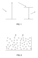
- Down-conversion represents a method for the generation of multiple electron-hole pairs, per incident high-energy photon, and can be used to reduce the thermalization losses. It is a material property that can be achieved if the material contains states or bands of intermediate energies. Incident high-energy photons can be transformed by the material into one or multiple lower energy photons. In a particular embodiment, the material is capable of emitting one photon per absorbed photon. FIG. 1 shows such energy levels of atoms in a down-converting material, and illustrates the process of down-conversion in which one photon of lower energy is produced. In some other embodiments, the material may emit more than one photon on absorption of one photon
- the down-converting layer comprises a phosphor material.
- such down-converting material contains a host material activated by a dopant (activator).
- a host material can be described as a transparent host lattice.
- a dopant adds desired energy levels at which incoming radiation is absorbed, such as an external photon, and a generated internal photon is preferentially emitted, based on the underlying absorber properties. Therefore, the down-converting material, at the basic level, contains an absorber and an emitter.
- dopant ions that may be used for 1 to 1 down-conversion include lanthanide ions, transition metal ions and rare-earth ions.
- suitable dopant ions include Ce 3+ , Eu 2+ , Sm 2+ , Cr 3+ , Mn 2+ and Mn 4+ .
- sensitizers may be doped into the host materials along with the dopants. Sensitizers are useful if the dopant ions cannot be excited, for example, because of forbidden transitions. The exciting energy is absorbed by the sensitizers and subsequently transferred to the dopant ions.
- transition metal ions may be sensitized by the lanthanide ions.
- FIG. 1 shows the emission of one photon as a result of absorption of a higher energy photon, it is possible to produce multiple photons per absorbed photon. In some embodiments, more than one photon is emitted per absorbed photon. This type of down-conversion is usually referred to as "quantum-cutting" or “quantum-splitting”. In some embodiments a sensitizer ion is also used for energy transfer to obtain more than one emitted low energy photon per absorbed high energy photon.
- a single dopant ion such as Pr 3+ , Tm 3+ or Gd 3+ , or a combination of two ions, such as the Gd 3+ -Eu 3+ dual ion, may be able to generate two low energy photons for every incident high-energy photon.
- Other combinations include Yb 3+ -Tb 3+ and Yb 3+ -Pr 3+ dual ions.
- Suitable examples of the phosphor material may include halides, oxides and phosphates.
- Suitable examples of fluorides include, but are not limited to, samarium-doped BaAlF 5 , samarium-doped (Ba, Sr, Ca)MgF 4 .
- Non-limiting examples of other suitable phosphors may include samarium-doped strontium borate (SrB 4 O 7 :Sm 2+ ), samarium-doped (Sr, Ca, Ba)BPO 5 and europium-doped (Sr, Ca)SiO 4 .
- an organic down-converting material may include an organic dye, such as BASF LUMOGEN dye.
- a hybrid organic-inorganic dye may also be used for down-conversion.
- the down converting material comprises a quantum dot, such as a shore-shell giant quantum dot system.
- the optical properties of the down-converting layer can be determined, in large part, by its material composition, particle size of down-converting material, thickness of the layer etc. By controlling the amount, particle size, and refractive index of the down-converting material, the refractive index and conversion properties of the down-converting layer may be tailored to minimize energy losses.
- the down-converting material may absorb radiation of a particular wavelength, or a particular range of wavelengths, while not scattering the radiation.
- the material may absorb radiation from UV, to visible, to near infrared, to infrared and converts the absorbed radiation to usable radiation.
- usable radiation refers to photons of a particular wavelength, or a particular range of wavelength that take part in energy conversion with high internal and external quantum efficiency. That is, the probability of collecting an electron-hole pair in that spectral range is high, usually greater than about 60%, and often greater than about 80%.
- the down-converting material emits such photons that can be absorbed by a semiconductor layer of the device to produce electron-hole pairs.
- the material absorbs radiation with wavelength below about 525 nm, and produces radiation with wavelength longer than 550 nm.
- the excitation and absorption properties of the down-converting layer, as well as the emission spectrum are designed to enhance external quantum efficiency (EQE) of the PV device.
- the material exhibits a refractive index value that should typically match well with refractive indices of adjacent mediums.
- This configuration advantageously provides reduced reflection at interfaces because of improved matching of refractive indices.
- the down-converting layer described herein benefits the photovoltaic device in two ways: (1) reduces absorption losses and (2) reduces reflection losses, and thus improves over all energy conversion.
- the down-converting layer has a uniform refractive index.
- the reflectance of the layer having a uniform refractive index may be minimum, for a particular wavelength.
- the down-converting layer may have a graded refractive index.
- the graded refractive index may be defined as a variation in the refractive index as a function of position in a selected direction, typically a direction perpendicular to a substrate supporting the layer.
- a value of refractive index at a first surface of the layer varies from a value of refractive index at a second surface of the layer.
- the variation in refractive index may be continuous in the selected direction or may occur in a series of discrete steps. In both the instances, the value of refractive index of the layer at a particular point is between the respective refractive indices of the glass plate and the transparent conductive layer.
- the gradient of refractive index can be achieved by compositional variations.
- the graded composition provides a graded refractive index to the layer.
- the "graded composition" as defined herein refers to a variation in the composition of the down-converting material in one direction, although the gradation may not always be constant. In this manner, the excitation and emission profile of the layer can be broadened, which will have beneficial effect of providing a coverage of broad wavelength ranges for the overall down-converting layer.
- the down-converting layer is a single layer.
- the down-converting layer includes more than one sub-layer. Multiple sub-layers of different refractive indices may be deposited, one over another, to attain the desired grading.
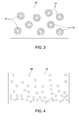
- the particles 10 of the down-converting material may be dispersed or embedded in a transparent matrix 12, as illustrated in FIG. 2 .
- the term "embedded” is used to indicate that the down-converting particles 10 are at least substantially enclosed within the matrix 12.
- the particles 10 are dispersed in such a manner that minimal agglomeration between the particles 10 is achieved.
- the refractive index of the matrix 12 may be higher than that of the down-converting material in some embodiments, and lower than that of the down-converting material in other embodiments.
- Such down-converting layer may also be referred to as “composite down-converting layer” and exhibit an "effective refractive index" which results from the combination of refraction due to particles and refraction due to the matrix (discussed in detail below).
- the effective refractive index of the composite down-converting layer depends on various parameters, such as refractive index of the matrix, refractive index of the down-converting material, and particle size of down-converting particles, among others.
- the refractive index of a medium is defined as the ratio of the velocity of light in a vacuum to that of the medium.
- Effective refractive index refers to refractive index of the composite down-converting layer having down-converting particles embedded in a matrix.
- the effective refractive index as defined herein, is used to determine the phase lag and attenuation of the coherent wave as electromagnetic radiation propagates through the layer.
- the parameters such as size, local volume fraction or area fraction, down-converting material fraction, matrix fraction and material refractive index, determine the effective refractive index of the layer.
- the refractive index of a material or medium may vary with wavelength. This effect is typically known as dispersion.
- the refractive indices of the down-converting material particles 10 and the matrix 12 may vary differently with wavelength.
- the dispersion of refractive indices for the down-converting particles 10 and the matrix 12 are chosen such that the refractive indices are well matched in the long wavelength range (> about 550 nanometers) of the solar spectrum so that scattering is minimized for incoming radiation in that range.
- the dispersion in the lower wavelength region specifically below about 525 nm, is chosen such that the refractive indices diverge such that photon-trapping in the composite layer can occur to improve absorption.
- the down-converting material may contain particles 10 of various shapes and sizes depending on refractive index of the constituents' materials, difference in refractive indices ( ⁇ n) and scattering effects.
- the size of particles is in part, a function of ⁇ n.
- nanosize particles of the down-converting material are desirable, especially for ⁇ n larger than about 0.05.
- nanosize refers to average size of the down-converting particles in a range from about 1 nanometer to about 500 nanometers, and in some specific embodiments, from about 10 nanometers to about 100 nanometers. In some other instances, bigger particles may be used for ⁇ n less than about 0.05. In these instances, the average particle size ranges from about 0.5 micron to about 10 microns, and in specific embodiments, from about 1 micron to about 5 microns.
- the matrix 12 may include a non-conductive, non-crystalline material such as glass.
- glasses may include soda-lime glass, alumino-silicate glass, boro-silicate glass, silica, and low-iron glass.
- the matrix 12 may include a non-conductive crystalline material.
- Other suitable materials such as a dielectric material or a hybrid organic-inorganic material may also be used.
- the down-converting material particles 10 may be present in the matrix 12 in any amount (percentage) that is appropriate for the desired function.
- the down-converting particles 10 may be present at a level of between about 0.001 % to about 60 % by volume, depending on the type of the matrix material and type of down-converting material.
- the percentage (amount) may be in a range of from about 10 % to about 25 % by volume.
- the down-converting materials may also contain additional layers on them, for the purposes of surface passivation or improved refractive index matching (e.g. a core-shell structure).
- FIG. 3 illustrates such an embodiment of core-shell structures 14 of down-converting particles 10 dispersed in the matrix 12.
- the particles 10 of down-converting material form the core, which are coated with one or more dielectric shell layers 16.
- the multiple shell layers 16 are configured such that they substantially match the refractive index of the matrix 12 on one side, and that of the phosphor particles 10 on the other.
- These shell layers 16 may allow for better optical coupling of incoming short wavelength radiation to the down-converting particles 10 so that scattering is reduced for the composite down-converting layer.
- the shell layers 16 may further allow for better out-coupling of down-converted long wavelength radiation into the matrix 12 of the composite layer.
- the down-converting particles 10 are coated with a thin layer of metal nanoparticles (not shown). These particles have strong plasmon resonance that helps to improve the emission efficiency (luminescent quantum efficiency) of down converted radiation from the down-converting particles 10.
- the metal nanoparticles are placed in direct contact with the down-converting particles 10, and in some other instances, the metal nanoparticles are separated by a thin dielectric shell that is first coated on the down-converting particles 10. The thickness of the shell layers may be about 1 nanometer to about 10 nanometers.
- These coated particles are then mixed with a liquid precursor matrix solution, which is deposited and solidified to form the composited down-converting layer.
- the down-converting particles 10 form a density gradient from a lower region to an upper region within the matrix 12. This density gradient provides gradation in refractive index of the layer in one direction, although the gradation may not always be constant.
- the down-converting layer is a single layer having density gradation as illustrated in FIG. 4 .
- FIG. 5 illustrates another embodiment where the down-converting layer includes more than one sub-layer 18. Multiple sub-layers 18 of varying density of down-converting particles 10 may be deposited, one over another, to attain the desired refractive index grading. In some instances, sub-layers 18 of different refractive indices may be separated by dielectric layers 20 as illustrated in FIG. 6 .
- Suitable dielectric materials include silicon oxide, silicon nitride, titanium oxide, hafnium oxide or combinations thereof.
- the dielectric layers 20 may act as back reflectors that minimizes transmission and reflects the photons emitted from the down-converting layer(s) back to the device.
- the down-converting layer has a thickness greater than about 100 nanometers.
- the thickness of the layer may be in a range of about 500 nanometers to about 1 micron.
- the thickness of each of the sub-layer may be in a range of about 500 nanometers to about 800 nanometers, in some instances.
- the down-converting layer has a thickness from about 1 micron to about 3000 microns, and in some specific embodiments from about 1 to about 100 microns.
- a down-converting layer characterized by a graded index profile provides good matching of refractive index at the interfaces, resulting in less reflection than may be achieved with uniform refractive index.
- the refractive index of the layer may increase or decrease with position from a first surface towards a second surface. Furthermore, the variation of the refractive index may also depend on the position of the layer in the device so that the values of refractive indices at the first and the second surfaces substantially match with the respective adjacent layers or mediums.
- the refractive index may increase in a direction extending from the first surface that is near to the glass plate, to the second surface, which is near to the transparent conductive oxide layer.
- the down-converting layer can be formed (deposited) by a variety of techniques, such as physical vapor deposition, chemical deposition, sputtering, solution growth, and solution deposition.
- Other suitable techniques include dip-coating, spray-coating, spin-coating, slot-die coating, roller coating, gravure printing, ink-jet printing, screen printing, capillary printing, tape casting, flexo coating, extrusion coating, and combinations thereof.
- the photovoltaic device is a thin-film heterojunction device, for example a CdTe PV device or a Cu(In,Ga,Al)(Se,S) 2 (also referred to as "CIGS") PV device.
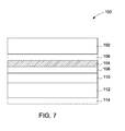
- FIG. 7 illustrates a thin film photovoltaic device 100, in one embodiment.
- the device 100 includes a glass plate 102 adjacent to which a down-converting layer 104 is disposed.
- a thin transparent dielectric layer 106 optionally may be disposed between the glass plate 102 and the down-converting layer 104. This dielectric layer 106 acts as a diffusion barrier for ions to enter the down-converting layer 104 and a PV cell from the glass plate 102.
- the glass plate 102 may have a substantially planar surface.
- a "substantially planar surface”, as defined herein, usually refers to a substantially flat surface.
- the surface can be smooth, although it may include a relatively minor degree (e.g., an RMS roughness that is less than about 1 micron, or more specifically less than about 300 nm) of texture, indentations, and various irregularities. These irregularities, textures, or patterns, may be useful in minimizing light trapping in the down-converting layer and channeling the converted radiation to the device by refraction at the dimpled surface.
- the glass plate 102 is a substrate.
- the glass plate 102 acts as a cover and the device 100 further includes a substrate 114.
- Substrate selection may include substrates of any suitable material, including, but not limited to, metal, semiconductor, doped semiconductor, amorphous dielectrics, crystalline dielectrics, and combinations thereof.
- a transparent conductive layer 108 is disposed adjacent to the down-converting layer 104 such that the down-converting layer is interposed between the glass plate 102 and the transparent conductive layer 108.
- Suitable materials for transparent conductive layer 108 may include an oxide, sulfide, phosphide, telluride, or combinations thereof. These transparent conductive materials may be doped or undoped.
- the conductive oxide may include titanium dioxide, silicon oxide, zinc oxide, tin oxide, aluminum doped zinc oxide, fluorine-doped tin oxide, cadmium stannate (cadmium tin oxide), or zinc stannate (zinc tin oxide).
- the conductive oxide includes indium-containing oxides.
- suitable indium containing oxides are indium tin oxide (ITO), Ga-In-Sn-O, Zn-In-Sn-O, Ga-In-O, Zn-In-O, and combinations thereof.
- Suitable sulfides may include cadmium sulfide, indium sulfide and the like.
- Suitable phosphides may include indium phosphide, gallium phosphide, and the like.
- a first type semiconductor layer 110 is disposed adjacent to the transparent conductive layer 108 and a second type semiconductor layer 112 is disposed adjacent to the first type semiconductor layer 110.
- the first type semiconductor layer 110 and the second type semiconductor layer 112 may be doped with a p-type doping or n-type doping such as to form a heterojunction.
- a heterojunction is a semiconductor junction, which is composed of layers of dissimilar semiconductor material. These materials usually have non-equal band gaps.
- a heterojunction can be formed by contact between a layer or region of one conductivity type with a layer or region of opposite conductivity, e.g., a "p-n" junction).
- other devices which utilize the heterojunction, include thin film transistors and bipolar transistors.
- the second type semiconductor material layer 112 includes an absorber layer.
- the absorber layer is a part of a photovoltaic device where the conversion of electromagnetic energy of incident light (for instance, sunlight) to electron-hole pairs (that is, to electrical current), occurs.
- a photo-active material is typically used for forming the absorber layer.
- the second type semiconductor material used for the absorber layer includes Cu(In,Ga,Al)(Se,S) 2 (also referred to as "CIGS"). In some instances, CIGS may further be substituted with an additional element, for example silver.
- CIGS layer or film may be manufactured by various known methods.
- Examples of such methods include vacuum-based processes, which co-evaporate, or co-sputter copper, gallium and indium, reactive sputtering, ion beam deposition, solution based deposition of nanoparticles precursors, and metal-organic chemical vapor deposition.
- Cadmium telluride is another photo-active material, which may be used for the absorber layer, in one embodiment.
- CdTe is an efficient photo-active material that is used in thin-film photovoltaic devices.
- CdTe is relatively easy to deposit and therefore is considered suitable for large-scale production.
- a typical method to deposit CdTe is closed-space sublimation.
- photovoltaic devices including CdTe as the photo-active material may be referred to as “CdTe PV devices” and those including CIGS may be referred to as “CIGS PV devices.”
- CdTe PV devices photovoltaic devices including CdTe PV devices
- CIGS PV devices those including CIGS may be referred to as “CIGS PV devices.”
- Other examples of photovoltaic devices, according to a photo-active material used in the device include a micromorph tandem silicon thin film cell, a copper-zinc-tin-sulfide (CZTS) thin film cell, a metal sulfide thin film cell and a metal phosphide thin film cell.
- CZTS copper-zinc-tin-sulfide
- the above-mentioned photo-active semiconductor materials may be used alone or in combination. Also, these materials may be present in more than one layer, each layer having different type of photo-active material or having combinations of the materials in separate layers.
- One of the ordinary skills in the art would be able to optimally configure the construction and the amount of the photo-active materials to maximize the efficiency of the photovoltaic cell.
- An example of the first type semiconductor 110 includes cadmium sulfide (CdS).
- Cadmium sulfide absorbs radiation strongly at wavelengths below about 500 nanometers and significantly reduces the quantum efficiency of a PV device in this wavelength region.
- the down-converting layer 104 is disposed on the device 100 in front of the cadmium sulfide layer 110 that may absorb radiation with wavelength lower than about 525 nanometers and convert them to longer wavelengths, in these instances.
- the photovoltaic module may have an array of a number of photovoltaic devices described above electrically connected to in series or in parallel. Substantially all photovoltaic devices include down-converting layer disposed on the device as discussed in above embodiments. In some embodiments, edges of the module are painted with a diffuse reflecting paint to reduce reflection and escape of emitted photon from the edge of the module
- 1.3 mm thick glass substrate is first coated with cerium-doped yttrium aluminum garnet oxide for down conversion. A layer of about 2 microns is deposited using RF sputtering technique. Subsequently, a CdTe PV cell is fabricated by depositing an indium tin oxide on the down-converting oxide layer, following by a CdS layer, and CdTe layer, and standard back contacts known in the art. Laser scribing is used to connect the CdTe PV cells in series to form a module. The scribe laser has wavelength longer than about 550 nm.
- Phosphor particles were formed by high temperature reaction process, followed by mechanical ball milling. Milling was continued for the time required to achieve desired particle size. These particles of desired amount were dispersed in a liquid glass precursor solution by mixing them ultrasonically.
- Phosphor particle of desired size are prepared as described in method I. Prior to incorporation in the liquid glass precursor solution, the particles are subject to TEOS- based chemistry in chemical baths for deposition of various transparent oxide layer on the particle surface. These shell layers provide a graded index on the particle surface that is more effectively allow light to enter the particles for down conversion.
- a composite solution is prepared as described in method I or II containing cerium-doped yttrium aluminum garnet oxide particles.
- the mean particle size of the oxide particles is about 100 nm, and difference in refractive indices is more than 0.05, i.e. about 1.7.
- the amount of particles in the precursor solution is about 33 weight percent.
- the composite solution is applied on a glass substrate to form a down-converting layer. Subsequently, a CdTe PV cell is fabricated as explained in example 1.
- Three different solutions are prepared with about 30 weight percent, about 20 weight percent, and about 10 weight percent of oxide particles in the precursor solution as described in example 3.
- the solution containing the lowest weight percent of particles is deposited on a glass substrate first, followed by a solution with the second high loading, and then a solution with the highest loading to form a down-converting layer. Subsequently, a CdTe PV cell is fabricated as explained in example 1.
Landscapes
- Photovoltaic Devices (AREA)
Applications Claiming Priority (1)
| Application Number | Priority Date | Filing Date | Title |
|---|---|---|---|
| US12/894,901 US20120080070A1 (en) | 2010-09-30 | 2010-09-30 | Photovoltaic devices |
Publications (2)
| Publication Number | Publication Date |
|---|---|
| EP2437313A2 true EP2437313A2 (de) | 2012-04-04 |
| EP2437313A3 EP2437313A3 (de) | 2013-05-29 |
Family
ID=44719432
Family Applications (1)
| Application Number | Title | Priority Date | Filing Date |
|---|---|---|---|
| EP11182364.7A Withdrawn EP2437313A3 (de) | 2010-09-30 | 2011-09-22 | Photovoltaische Vorrichtungen |
Country Status (4)
| Country | Link |
|---|---|
| US (1) | US20120080070A1 (de) |
| EP (1) | EP2437313A3 (de) |
| CN (1) | CN102446988A (de) |
| AU (1) | AU2011226900A1 (de) |
Families Citing this family (5)
| Publication number | Priority date | Publication date | Assignee | Title |
|---|---|---|---|---|
| DE102011016567B4 (de) * | 2011-04-08 | 2023-05-11 | OSRAM Opto Semiconductors Gesellschaft mit beschränkter Haftung | Verfahren zum Herstellen eines optoelektronischen Bauelements und derart hergestelltes Bauelement |
| US8981305B2 (en) * | 2011-05-12 | 2015-03-17 | University Of Florida Research Foundation, Inc. | Index of refraction matched nanoparticles and methods of use |
| KR101952119B1 (ko) * | 2012-05-24 | 2019-02-28 | 삼성전자 주식회사 | 메탈 실리사이드를 포함하는 반도체 장치 및 이의 제조 방법 |
| US20170341346A1 (en) * | 2016-05-25 | 2017-11-30 | Ubiqd, Llc | Laminated glass luminescent concentrator |
| NL2021109B1 (en) | 2018-06-12 | 2019-12-17 | Physee Group B V | Inorganic luminescent materials for solar radiation conversion devices |
Family Cites Families (9)
| Publication number | Priority date | Publication date | Assignee | Title |
|---|---|---|---|---|
| CN101405088A (zh) * | 2005-11-10 | 2009-04-08 | 伊利诺伊大学受托管理委员会 | 硅纳米颗粒光伏装置 |
| KR100746749B1 (ko) * | 2006-03-15 | 2007-08-09 | (주)케이디티 | 광 여기 시트 |
| US8197720B2 (en) * | 2007-01-22 | 2012-06-12 | Konica Minolta Medical & Graphic, Inc. | Core/shell type semiconductor nanoparticle and method for production thereof |
| US20100294339A1 (en) * | 2007-07-17 | 2010-11-25 | Miasole | photovoltaic device with a luminescent down-shifting material |
| US8039736B2 (en) * | 2008-08-18 | 2011-10-18 | Andrew Clark | Photovoltaic up conversion and down conversion using rare earths |
| US20090084963A1 (en) * | 2007-10-01 | 2009-04-02 | David, Joseph And Negley | Apparatus and methods to produce electrical energy by enhanced down-conversion of photons |
| WO2009099568A1 (en) * | 2008-01-31 | 2009-08-13 | The Board Of Trustees Of The Leland Stanford Junior University | Applicable fluorescence of diamondoids |
| US20090255577A1 (en) * | 2008-04-04 | 2009-10-15 | Michael Tischler | Conversion Solar Cell |
| TW201005972A (en) * | 2008-07-17 | 2010-02-01 | Nexpower Technology Corp | Thin film solar cell having photo-luminescent medium coated therein and manufacturing method thereof |
-
2010
- 2010-09-30 US US12/894,901 patent/US20120080070A1/en not_active Abandoned
-
2011
- 2011-09-22 EP EP11182364.7A patent/EP2437313A3/de not_active Withdrawn
- 2011-09-27 AU AU2011226900A patent/AU2011226900A1/en not_active Abandoned
- 2011-09-29 CN CN2011103096638A patent/CN102446988A/zh active Pending
Non-Patent Citations (1)
| Title |
|---|
| None |
Also Published As
| Publication number | Publication date |
|---|---|
| CN102446988A (zh) | 2012-05-09 |
| AU2011226900A1 (en) | 2012-04-19 |
| US20120080070A1 (en) | 2012-04-05 |
| EP2437313A3 (de) | 2013-05-29 |
Similar Documents
| Publication | Publication Date | Title |
|---|---|---|
| EP2437315A2 (de) | Photovoltaische Vorrichtungen | |
| KR101000057B1 (ko) | 다층 투명전도층을 구비한 태양전지 이의 제조방법 | |
| KR101575733B1 (ko) | 근적외선 파장변환 구조체 및 이를 이용한 태양전지 | |
| CN102810572A (zh) | 用于光伏装置的薄膜层的折射率匹配及其制造方法 | |
| WO2010096721A2 (en) | Solar modules including spectral concentrators and related manufacturing methods | |
| MX2013015438A (es) | Un panel espectralmente selectivo. | |
| EP2437314A2 (de) | Photovoltaische Vorrichtungen | |
| WO2011071738A2 (en) | Luminescent materials that emit light in the visible range or the near infrared range and methods of forming thereof | |
| TW201222843A (en) | Transparent electrically conductive substrate carrying thereon a surface electrode, a manufacturing method therefor, a thin-film solar cell and a manufacturing method therefor | |
| CA2886431A1 (en) | Photovoltaic component with a high conversion efficiency | |
| US12268037B2 (en) | Tandem photovoltaic device | |
| EP2437313A2 (de) | Photovoltaische Vorrichtungen | |
| CN104081544B (zh) | 用于硅基光电装置的高功函数缓冲层 | |
| US20100043872A1 (en) | Photovoltaic Device With an Up-Converting Quantum Dot Layer and Absorber | |
| Chaudhary et al. | Upconversion as a spear carrier for tuning photovoltaic efficiency | |
| US20100044675A1 (en) | Photovoltaic Device With an Up-Converting Quantum Dot Layer | |
| JP2007288043A (ja) | 光電変換装置用透明導電膜とその製造方法 | |
| KR101404243B1 (ko) | 형광체를 포함하는 태양전지 및 이의 제조방법 | |
| JP2011151068A (ja) | 光電変換装置 | |
| JP2005347444A (ja) | 光起電力素子 | |
| US8993878B2 (en) | Electrode for photovoltaic device | |
| US20130247994A1 (en) | Photovoltaic device | |
| Idutsu et al. | Intrinsic luminescence-downshifting effects of Zn-based Mn-doped nanoparticle layers on Si solar cells | |
| EP2437289A2 (de) | Photovoltaikvorrichtung und Herstellungsverfahren | |
| KR20110077923A (ko) | 박막 태양전지의 전면 전극 및 그를 포함하는 박막 실리콘 태양전지 |
Legal Events
| Date | Code | Title | Description |
|---|---|---|---|
| PUAI | Public reference made under article 153(3) epc to a published international application that has entered the european phase |
Free format text: ORIGINAL CODE: 0009012 |
|
| AK | Designated contracting states |
Kind code of ref document: A2 Designated state(s): AL AT BE BG CH CY CZ DE DK EE ES FI FR GB GR HR HU IE IS IT LI LT LU LV MC MK MT NL NO PL PT RO RS SE SI SK SM TR |
|
| AX | Request for extension of the european patent |
Extension state: BA ME |
|
| PUAL | Search report despatched |
Free format text: ORIGINAL CODE: 0009013 |
|
| AK | Designated contracting states |
Kind code of ref document: A3 Designated state(s): AL AT BE BG CH CY CZ DE DK EE ES FI FR GB GR HR HU IE IS IT LI LT LU LV MC MK MT NL NO PL PT RO RS SE SI SK SM TR |
|
| AX | Request for extension of the european patent |
Extension state: BA ME |
|
| RIC1 | Information provided on ipc code assigned before grant |
Ipc: H01L 31/055 20060101AFI20130425BHEP |
|
| 17P | Request for examination filed |
Effective date: 20131128 |
|
| RBV | Designated contracting states (corrected) |
Designated state(s): AL AT BE BG CH CY CZ DE DK EE ES FI FR GB GR HR HU IE IS IT LI LT LU LV MC MK MT NL NO PL PT RO RS SE SI SK SM TR |
|
| RAP1 | Party data changed (applicant data changed or rights of an application transferred) |
Owner name: FIRST SOLAR MALAYSIA SDN.BHD |
|
| STAA | Information on the status of an ep patent application or granted ep patent |
Free format text: STATUS: THE APPLICATION IS DEEMED TO BE WITHDRAWN |
|
| 18D | Application deemed to be withdrawn |
Effective date: 20131130 |