EP2437288A1 - Compatible vertical double diffused metal oxide semiconductor transistor and lateral double diffused metal oxide semiconductor transistor and manufacture method thereof - Google Patents
Compatible vertical double diffused metal oxide semiconductor transistor and lateral double diffused metal oxide semiconductor transistor and manufacture method thereof Download PDFInfo
- Publication number
- EP2437288A1 EP2437288A1 EP10826075A EP10826075A EP2437288A1 EP 2437288 A1 EP2437288 A1 EP 2437288A1 EP 10826075 A EP10826075 A EP 10826075A EP 10826075 A EP10826075 A EP 10826075A EP 2437288 A1 EP2437288 A1 EP 2437288A1
- Authority
- EP
- European Patent Office
- Prior art keywords
- area
- transistor
- ldmos transistor
- vdmos
- epitaxial layer
- Prior art date
- Legal status (The legal status is an assumption and is not a legal conclusion. Google has not performed a legal analysis and makes no representation as to the accuracy of the status listed.)
- Ceased
Links
Images

Classifications
-
- H—ELECTRICITY
- H10—SEMICONDUCTOR DEVICES; ELECTRIC SOLID-STATE DEVICES NOT OTHERWISE PROVIDED FOR
- H10D—INORGANIC ELECTRIC SEMICONDUCTOR DEVICES
- H10D30/00—Field-effect transistors [FET]
- H10D30/01—Manufacture or treatment
- H10D30/021—Manufacture or treatment of FETs having insulated gates [IGFET]
- H10D30/028—Manufacture or treatment of FETs having insulated gates [IGFET] of double-diffused metal oxide semiconductor [DMOS] FETs
- H10D30/0291—Manufacture or treatment of FETs having insulated gates [IGFET] of double-diffused metal oxide semiconductor [DMOS] FETs of vertical DMOS [VDMOS] FETs
-
- H—ELECTRICITY
- H10—SEMICONDUCTOR DEVICES; ELECTRIC SOLID-STATE DEVICES NOT OTHERWISE PROVIDED FOR
- H10D—INORGANIC ELECTRIC SEMICONDUCTOR DEVICES
- H10D84/00—Integrated devices formed in or on semiconductor substrates that comprise only semiconducting layers, e.g. on Si wafers or on GaAs-on-Si wafers
- H10D84/01—Manufacture or treatment
- H10D84/0123—Integrating together multiple components covered by H10D12/00 or H10D30/00, e.g. integrating multiple IGBTs
- H10D84/0126—Integrating together multiple components covered by H10D12/00 or H10D30/00, e.g. integrating multiple IGBTs the components including insulated gates, e.g. IGFETs
- H10D84/013—Manufacturing their source or drain regions, e.g. silicided source or drain regions
-
- H—ELECTRICITY
- H10—SEMICONDUCTOR DEVICES; ELECTRIC SOLID-STATE DEVICES NOT OTHERWISE PROVIDED FOR
- H10D—INORGANIC ELECTRIC SEMICONDUCTOR DEVICES
- H10D84/00—Integrated devices formed in or on semiconductor substrates that comprise only semiconducting layers, e.g. on Si wafers or on GaAs-on-Si wafers
- H10D84/01—Manufacture or treatment
- H10D84/0123—Integrating together multiple components covered by H10D12/00 or H10D30/00, e.g. integrating multiple IGBTs
- H10D84/0126—Integrating together multiple components covered by H10D12/00 or H10D30/00, e.g. integrating multiple IGBTs the components including insulated gates, e.g. IGFETs
- H10D84/016—Integrating together multiple components covered by H10D12/00 or H10D30/00, e.g. integrating multiple IGBTs the components including insulated gates, e.g. IGFETs the components including vertical IGFETs
-
- H—ELECTRICITY
- H10—SEMICONDUCTOR DEVICES; ELECTRIC SOLID-STATE DEVICES NOT OTHERWISE PROVIDED FOR
- H10D—INORGANIC ELECTRIC SEMICONDUCTOR DEVICES
- H10D84/00—Integrated devices formed in or on semiconductor substrates that comprise only semiconducting layers, e.g. on Si wafers or on GaAs-on-Si wafers
- H10D84/01—Manufacture or treatment
- H10D84/02—Manufacture or treatment characterised by using material-based technologies
- H10D84/03—Manufacture or treatment characterised by using material-based technologies using Group IV technology, e.g. silicon technology or silicon-carbide [SiC] technology
- H10D84/038—Manufacture or treatment characterised by using material-based technologies using Group IV technology, e.g. silicon technology or silicon-carbide [SiC] technology using silicon technology, e.g. SiGe
-
- H—ELECTRICITY
- H10—SEMICONDUCTOR DEVICES; ELECTRIC SOLID-STATE DEVICES NOT OTHERWISE PROVIDED FOR
- H10D—INORGANIC ELECTRIC SEMICONDUCTOR DEVICES
- H10D84/00—Integrated devices formed in or on semiconductor substrates that comprise only semiconducting layers, e.g. on Si wafers or on GaAs-on-Si wafers
- H10D84/80—Integrated devices formed in or on semiconductor substrates that comprise only semiconducting layers, e.g. on Si wafers or on GaAs-on-Si wafers characterised by the integration of at least one component covered by groups H10D12/00 or H10D30/00, e.g. integration of IGFETs
- H10D84/82—Integrated devices formed in or on semiconductor substrates that comprise only semiconducting layers, e.g. on Si wafers or on GaAs-on-Si wafers characterised by the integration of at least one component covered by groups H10D12/00 or H10D30/00, e.g. integration of IGFETs of only field-effect components
- H10D84/83—Integrated devices formed in or on semiconductor substrates that comprise only semiconducting layers, e.g. on Si wafers or on GaAs-on-Si wafers characterised by the integration of at least one component covered by groups H10D12/00 or H10D30/00, e.g. integration of IGFETs of only field-effect components of only insulated-gate FETs [IGFET]
-
- H—ELECTRICITY
- H10—SEMICONDUCTOR DEVICES; ELECTRIC SOLID-STATE DEVICES NOT OTHERWISE PROVIDED FOR
- H10D—INORGANIC ELECTRIC SEMICONDUCTOR DEVICES
- H10D84/00—Integrated devices formed in or on semiconductor substrates that comprise only semiconducting layers, e.g. on Si wafers or on GaAs-on-Si wafers
- H10D84/80—Integrated devices formed in or on semiconductor substrates that comprise only semiconducting layers, e.g. on Si wafers or on GaAs-on-Si wafers characterised by the integration of at least one component covered by groups H10D12/00 or H10D30/00, e.g. integration of IGFETs
- H10D84/82—Integrated devices formed in or on semiconductor substrates that comprise only semiconducting layers, e.g. on Si wafers or on GaAs-on-Si wafers characterised by the integration of at least one component covered by groups H10D12/00 or H10D30/00, e.g. integration of IGFETs of only field-effect components
- H10D84/83—Integrated devices formed in or on semiconductor substrates that comprise only semiconducting layers, e.g. on Si wafers or on GaAs-on-Si wafers characterised by the integration of at least one component covered by groups H10D12/00 or H10D30/00, e.g. integration of IGFETs of only field-effect components of only insulated-gate FETs [IGFET]
- H10D84/83125—Integrated devices formed in or on semiconductor substrates that comprise only semiconducting layers, e.g. on Si wafers or on GaAs-on-Si wafers characterised by the integration of at least one component covered by groups H10D12/00 or H10D30/00, e.g. integration of IGFETs of only field-effect components of only insulated-gate FETs [IGFET] the IGFETs characterised by having shared source or drain regions
-
- H—ELECTRICITY
- H10—SEMICONDUCTOR DEVICES; ELECTRIC SOLID-STATE DEVICES NOT OTHERWISE PROVIDED FOR
- H10D—INORGANIC ELECTRIC SEMICONDUCTOR DEVICES
- H10D84/00—Integrated devices formed in or on semiconductor substrates that comprise only semiconducting layers, e.g. on Si wafers or on GaAs-on-Si wafers
- H10D84/80—Integrated devices formed in or on semiconductor substrates that comprise only semiconducting layers, e.g. on Si wafers or on GaAs-on-Si wafers characterised by the integration of at least one component covered by groups H10D12/00 or H10D30/00, e.g. integration of IGFETs
- H10D84/82—Integrated devices formed in or on semiconductor substrates that comprise only semiconducting layers, e.g. on Si wafers or on GaAs-on-Si wafers characterised by the integration of at least one component covered by groups H10D12/00 or H10D30/00, e.g. integration of IGFETs of only field-effect components
- H10D84/83—Integrated devices formed in or on semiconductor substrates that comprise only semiconducting layers, e.g. on Si wafers or on GaAs-on-Si wafers characterised by the integration of at least one component covered by groups H10D12/00 or H10D30/00, e.g. integration of IGFETs of only field-effect components of only insulated-gate FETs [IGFET]
- H10D84/835—Integrated devices formed in or on semiconductor substrates that comprise only semiconducting layers, e.g. on Si wafers or on GaAs-on-Si wafers characterised by the integration of at least one component covered by groups H10D12/00 or H10D30/00, e.g. integration of IGFETs of only field-effect components of only insulated-gate FETs [IGFET] comprising LDMOS
-
- H—ELECTRICITY
- H10—SEMICONDUCTOR DEVICES; ELECTRIC SOLID-STATE DEVICES NOT OTHERWISE PROVIDED FOR
- H10D—INORGANIC ELECTRIC SEMICONDUCTOR DEVICES
- H10D84/00—Integrated devices formed in or on semiconductor substrates that comprise only semiconducting layers, e.g. on Si wafers or on GaAs-on-Si wafers
- H10D84/80—Integrated devices formed in or on semiconductor substrates that comprise only semiconducting layers, e.g. on Si wafers or on GaAs-on-Si wafers characterised by the integration of at least one component covered by groups H10D12/00 or H10D30/00, e.g. integration of IGFETs
- H10D84/82—Integrated devices formed in or on semiconductor substrates that comprise only semiconducting layers, e.g. on Si wafers or on GaAs-on-Si wafers characterised by the integration of at least one component covered by groups H10D12/00 or H10D30/00, e.g. integration of IGFETs of only field-effect components
- H10D84/83—Integrated devices formed in or on semiconductor substrates that comprise only semiconducting layers, e.g. on Si wafers or on GaAs-on-Si wafers characterised by the integration of at least one component covered by groups H10D12/00 or H10D30/00, e.g. integration of IGFETs of only field-effect components of only insulated-gate FETs [IGFET]
- H10D84/837—Integrated devices formed in or on semiconductor substrates that comprise only semiconducting layers, e.g. on Si wafers or on GaAs-on-Si wafers characterised by the integration of at least one component covered by groups H10D12/00 or H10D30/00, e.g. integration of IGFETs of only field-effect components of only insulated-gate FETs [IGFET] comprising vertical IGFETs
- H10D84/839—Integrated devices formed in or on semiconductor substrates that comprise only semiconducting layers, e.g. on Si wafers or on GaAs-on-Si wafers characterised by the integration of at least one component covered by groups H10D12/00 or H10D30/00, e.g. integration of IGFETs of only field-effect components of only insulated-gate FETs [IGFET] comprising vertical IGFETs comprising VDMOS
-
- H—ELECTRICITY
- H10—SEMICONDUCTOR DEVICES; ELECTRIC SOLID-STATE DEVICES NOT OTHERWISE PROVIDED FOR
- H10D—INORGANIC ELECTRIC SEMICONDUCTOR DEVICES
- H10D30/00—Field-effect transistors [FET]
- H10D30/01—Manufacture or treatment
- H10D30/021—Manufacture or treatment of FETs having insulated gates [IGFET]
- H10D30/0221—Manufacture or treatment of FETs having insulated gates [IGFET] having asymmetry in the channel direction, e.g. lateral high-voltage MISFETs having drain offset region or extended-drain MOSFETs [EDMOS]
-
- H—ELECTRICITY
- H10—SEMICONDUCTOR DEVICES; ELECTRIC SOLID-STATE DEVICES NOT OTHERWISE PROVIDED FOR
- H10D—INORGANIC ELECTRIC SEMICONDUCTOR DEVICES
- H10D30/00—Field-effect transistors [FET]
- H10D30/60—Insulated-gate field-effect transistors [IGFET]
- H10D30/601—Insulated-gate field-effect transistors [IGFET] having lightly-doped drain or source extensions, e.g. LDD IGFETs or DDD IGFETs
- H10D30/603—Insulated-gate field-effect transistors [IGFET] having lightly-doped drain or source extensions, e.g. LDD IGFETs or DDD IGFETs having asymmetry in the channel direction, e.g. lateral high-voltage MISFETs having drain offset region or extended drain IGFETs [EDMOS]
-
- H—ELECTRICITY
- H10—SEMICONDUCTOR DEVICES; ELECTRIC SOLID-STATE DEVICES NOT OTHERWISE PROVIDED FOR
- H10D—INORGANIC ELECTRIC SEMICONDUCTOR DEVICES
- H10D30/00—Field-effect transistors [FET]
- H10D30/60—Insulated-gate field-effect transistors [IGFET]
- H10D30/64—Double-diffused metal-oxide semiconductor [DMOS] FETs
- H10D30/66—Vertical DMOS [VDMOS] FETs
- H10D30/663—Vertical DMOS [VDMOS] FETs having both source contacts and drain contacts on the same surface, i.e. up-drain VDMOS
-
- H—ELECTRICITY
- H10—SEMICONDUCTOR DEVICES; ELECTRIC SOLID-STATE DEVICES NOT OTHERWISE PROVIDED FOR
- H10D—INORGANIC ELECTRIC SEMICONDUCTOR DEVICES
- H10D62/00—Semiconductor bodies, or regions thereof, of devices having potential barriers
- H10D62/10—Shapes, relative sizes or dispositions of the regions of the semiconductor bodies; Shapes of the semiconductor bodies
- H10D62/13—Semiconductor regions connected to electrodes carrying current to be rectified, amplified or switched, e.g. source or drain regions
- H10D62/149—Source or drain regions of field-effect devices
- H10D62/151—Source or drain regions of field-effect devices of IGFETs
-
- H—ELECTRICITY
- H10—SEMICONDUCTOR DEVICES; ELECTRIC SOLID-STATE DEVICES NOT OTHERWISE PROVIDED FOR
- H10D—INORGANIC ELECTRIC SEMICONDUCTOR DEVICES
- H10D64/00—Electrodes of devices having potential barriers
- H10D64/20—Electrodes characterised by their shapes, relative sizes or dispositions
- H10D64/27—Electrodes not carrying the current to be rectified, amplified, oscillated or switched, e.g. gates
- H10D64/311—Gate electrodes for field-effect devices
- H10D64/411—Gate electrodes for field-effect devices for FETs
- H10D64/511—Gate electrodes for field-effect devices for FETs for IGFETs
- H10D64/514—Gate electrodes for field-effect devices for FETs for IGFETs characterised by the insulating layers
- H10D64/516—Gate electrodes for field-effect devices for FETs for IGFETs characterised by the insulating layers the thicknesses being non-uniform
-
- H—ELECTRICITY
- H10—SEMICONDUCTOR DEVICES; ELECTRIC SOLID-STATE DEVICES NOT OTHERWISE PROVIDED FOR
- H10D—INORGANIC ELECTRIC SEMICONDUCTOR DEVICES
- H10D84/00—Integrated devices formed in or on semiconductor substrates that comprise only semiconducting layers, e.g. on Si wafers or on GaAs-on-Si wafers
- H10D84/01—Manufacture or treatment
- H10D84/0107—Integrating at least one component covered by H10D12/00 or H10D30/00 with at least one component covered by H10D8/00, H10D10/00 or H10D18/00, e.g. integrating IGFETs with BJTs
- H10D84/0109—Integrating at least one component covered by H10D12/00 or H10D30/00 with at least one component covered by H10D8/00, H10D10/00 or H10D18/00, e.g. integrating IGFETs with BJTs the at least one component covered by H10D12/00 or H10D30/00 being a MOS device
Definitions
- the present invention relates to the field of fabricating a semiconductor device and in particular to an LDMOS transistor compatible with a VDMOS transistor and a method for fabricating the same.
- CMOS Complementary Metal Oxide Semiconductor
- DMOS Double-diffused Metal Oxide Semiconductor
- the BIPOLAR is intended for analogy control
- the CMOS is intended for digital control
- the DMOS is intended to enable soft startup and power output of a system in the case of the processing of high voltage and large current occurring in management in chip or system. Since respective advantages of the three kinds of devices are integrated in the BCD process, a BCD-based product can be can be integrated with a complex control function so that it has become a predominant process of power integrated circuits. For the BCD process, different devices can be selected for a varying circuit to optimize corresponding sub-circuits, thereby accommodating requirements on low power consumption, high integration, high speed, a high driving capability and large current of the entire circuit.
- High voltage MOS transistors in the existing BCD process are primarily Laterally Double-diffused Metal Oxide Semiconductors (LDMOS).
- Fig.1 illustrates the steps of forming an LDMOS transistor in the existing BCD process, where a substrate is prepared, the substrate can be made of silicon, silicon-germanium, etc.; boron ions are injected into the substrate to form an N-buried layer area 101; an N-epitaxial layer is formed on the N-buried layer area 101 by an epitaxial method; a first photoresist layer (not illustrated) is formed on the N-epitaxial layer, and an N-well pattern is defined by lithograph process; phosphorus ions are injected into the N-epitaxial layer along the N-well pattern using the first photoresist layer as a mask to form an N-well 102; a second photoresist layer (not illustrated) is formed on the N-epitaxial layer after the first photoresist layer is removed, and a P-well pattern is defined by lithograph
- a LOCal Oxidation of Silicon (LOCOS) isolation area 104 is formed at the interface between the N-well 102 and the P-well 103 by a field oxidation method after the second photoresist layer is removed; a third photoresist layer (not illustrated) is formed on the N-epitaxial layer, and a drift area pattern is defined in the area of the P-well 103 by lithograph process; phosphorus ions are injected into the N-epitaxial layer along the drift area pattern using the third photoresist layer as a mask, and an annealing process is performed to form a drift area 106a; and then the epitaxial layer of the drift area 106a is oxidized in a wet oxygen thermal oxidization method using the third photoresist layer again as a mask to form an LOCOS field plate 106b; and next the third photoresist layer is removed.
- LOCOS LOCal Oxidation of Silicon
- a polysilicon layer and a fourth photoresist layer are formed sequentially on the N-epitaxial layer, and a gate pattern is defined on the fourth photoresist layer after exposure and development processes; and the polysilicon layer is etched along the gate pattern using the fourth photoresist layer as a mask, a gate108 is formed on parts of the N-epitaxial layer and the drift area in the area of the P-well 103, and the fourth photoresist layer is removed.
- a fifth photoresist layer (not illustrated) is formed on the N-epitaxial layer, the LOCal Oxidation of Silicon (LOCOS) isolation area 104 and the gate 108, and a PBODY (P-type substrate concentration transition) area pattern is defined on the fifth photoresist layer between the gate 108 in the area of the P-well 103 and the LOCal Oxidation of Silicon (LOCOS) isolation area 104 after the exposure and development processes; and phosphorus ions are injected into the N-epitaxial layer along the PBODY area pattern using the fifth photoresist layer as a mask to form a PBODY area 109, wherein the PBODY 109 functions to form an active channel from a difference between its transverse diffusion length and that of a source/drain to control the threshold voltage of an LDMOS.
- LDMOS LOCal Oxidation of Silicon
- a sixth photoresist layer (not illustrated) is formed on the N-epitaxial layer, the LOCal Oxidation of Silicon (LOCOS) isolation area 104 and the gate 108 after the fifth photoresist layer is removed, and an opening pattern is defined on the sixth photoresist layer between the drift areas 106 after the exposure and development processes; phosphorus ions are injected into the N-epitaxial layer along the opening pattern using the sixth photoresist layer as a mask, and the annealing process is performed to diffuse uniformly the phosphorus ions into a larger depth so as to form an N-type GRADE (concentration gradient) area 110, wherein the GRADE area functions to form N-type ions with a low concentration outside of the source/drain, to reduce the dope dose of PN junction and to increase the breakdown voltage of the junction.
- the sixth photoresist layer is removed.
- an eighth photoresist layer (not illustrated) is formed on the N-epitaxial layer, the LOCal Oxidation of Silicon (LOCOS) isolation area 104 and the gate 108 after the seventh photoresist layer is removed, and a P+ area pattern is defined by lithograph process; and boron ions are injected into the PBODY area 109 in the N-epitaxial layer along the P+ area pattern using the eighth photoresist layer as a mask to form a P+ area 112, wherein the P+ area 112 is connected with the source S and functions to prevent a substrate electrode and the source from being shorted and to alleviate a substrate bias effect.
- the eighth photoresist layer is removed.
- VDMOS Vertical Double-diffused Metal Oxide Semiconductor
- the invention address the issue of providing a method for fabricating an LDMOS transistor compatible with a VDMOS transistor to address the impossibility of the BCD process to offer an LDMOS transistor compatible with a VDMOS transistor.
- the invention provides a method for fabricating an LDMOS transistor compatible with a VDMOS transistor including: preparing a substrate with an LDMOS transistor area and a VDMOS transistor area; forming an N-buried layer area by injecting ions into the substrate; forming an epitaxial layer in the N-buried layer area and then injecting ions into the epitaxial layer to form an N-well and a P-well in the LDMOS transistor area and a high voltage N-well in the VDMOS transistor area; forming an isolation area at the interface between the N-well and the P-well in the LDMOS transistor area and at the interface between the LDMOS transistor area and the VDMOS transistor area; forming a drift area in the area of the P-well in the LDMOS transistor area; forming a gate on a part of the epitaxial layer and a part of the drift area in the area of the P-well of the LDMOS transistor area, and in the VDMOS transistor area; forming a PBODY area in the
- the ions injected to form the NSINK area are phosphorus ions, which are injected at a dosage of 1 ⁇ 1015/cm2 and energy of 300KeV ⁇ 400KeV.
- the ions injected to form the N-buried layer area are antimony ions, which are injected at a dosage of 1 ⁇ 1015/cm2 and energy of 40KeV
- forming the drift area further includes: injecting phosphorus ions into a part of the area of the P well to form the drift area; and performing an oxidization process in the drift area to form an LOCOS field plate.
- the phosphorus ions are injected at a dosage of 1 ⁇ 1012/cm2 and energy of 40KeV ⁇ 50KeV
- the drift area is oxidized by a wet oxygen thermal oxidization method.
- the ions injected to form the PBODY area are boron ions, which are injected at a dosage of 2 ⁇ 1013/cm2 and energy of 40KeV
- the ions injected to form the N-type GRADE area are phosphorus ions, which are injected at a dosage of 1 ⁇ 1013/cm2 and energy of 80KeV ⁇ 100KeV
- the ions injected to form the source/drain are arsenic ions, which are injected at a dosage of 4 ⁇ 1015/cm2 and energy of 80KeV
- the ions injected to form the P+ area are formed boron difluoride, which are injected at a dosage of 2 ⁇ 1015/cm2 and energy of 60KeV ⁇ 80KeV
- the invention further provides an LDMOS transistor compatible with a VDMOS transistor, including: a substrate with an LDMOS transistor area and a VDMOS transistor area; an N-buried layer area located in the substrate; an epitaxial layer located in the N-buried layer area; an N-well and a P-well adjoining the N-well, which are formed in the epitaxial layer of the LDMOS transistor area; a high voltage N-well formed in the VDMOS transistor area; an isolation area located at the interface between the N-well and the P-well in the LDMOS transistor area and at the interface between the LDMOS transistor area and the VDMOS transistor area; a drift area located in the area of the P-well in the LDMOS transistor area; a gate located on a part of the epitaxial layer and a part of the drift area in the area of the P-well of the LDMOS transistor area, and on the epitaxial layer of the VDMOS transistor area; a PBODY area located in the epitaxial layer between the gate and the isolation area in the L
- the invention has such an advantage that the NSINK area is formed in the epitaxial layer between the isolation area and the adjacent gate in the VDMOS transistor area, and the NSINK area is communicated with the N-buried layer area, which enables communication between the drains, thereby achieving compatibility of an LDMOS transistor with a VDMOS transistor on a BCD process platform and further accommodating a performance demand for high voltage and large current.
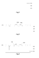
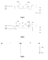
- Fig.1 to Fig.5 illustrate schematic diagrams of forming an LDMOS transistor in the existing BCD process
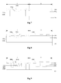
- Fig.6 to Fig. 11 illustrate schematic diagrams of a method for fabricating an LDMOS transistor compatible with a VDMOS transistor according to the invention.
- a substrate is prepared with an LDMOS transistor area and a VDMOS transistor area; ions are injected into the substrate to form an N-buried layer area; an epitaxial layer is formed in the N-buried layer area, and then ions are injected into the epitaxial layer to form an N-well and a P-well in the LDMOS transistor area and a high voltage N-well in the VDMOS transistor area; an isolation area is formed at the interface between the N-well and the P-well in the LDMOS transistor area and at the interface between the LDMOS transistor area and the VDMOS transistor area; a drift area is formed in the area of the P-well of the LDMOS transistor area; a gate is formed on a part of the epitaxial layer and a part of the drift area in the area of the P-well of the LDMOS transistor area, and in the VDMOS transistor area; a PBODY area is formed in the epitaxial layer between
- the invention forms the NSINK area in the epitaxial layer between the isolation area and the adjacent gate in the VDMOS transistor area and the NSINK area is communicated with the N-buried layer area, which enables communication between the drains, thereby achieving compatibility of an LDMOS transistor with a VDMOS transistor on a BCD process platform and further accommodating a performance demand for high voltage and large current.
- Fig.6 to Fig.11 illustrate schematic diagrams of a method for fabricating an LDMOS transistor compatible with a VDMOS transistor according to the invention.
- a substrate is prepared, wherein the substrate can be made of silicon, silicon-germanium, etc., and has an LDMOS transistor area I and a VDMOS transistor area II.
- N-type ions are injected into the substrate to form an N-buried layer area 201.
- the N-type ions can be antimony ions and are injected at a dosage of 1 ⁇ 1015/cm2 and energy of approximately 40KeV
- an N-epitaxial layer 202 with a thickness of approximately 4 ⁇ m is formed on the N-buried layer area 201 by epitaxial growth method.
- a first photoresist layer (not illustrated) is formed on the N-epitaxial layer, and an N-well pattern is defined in the LDMOS transistor area I by lithograph process; and N-type ions are injected into the N-epitaxial layer along the N-well pattern using the first photoresist layer as a mask to form an N-well 202a, the N-type ions can be phosphorus ions and are injected at a dosage of 6 ⁇ 1012/cm2 ⁇ 8 ⁇ 1012/cm2 and energy of approximately 150KeV
- a second photoresist layer (not illustrated) is formed on the N-epitaxial layer after the first photoresist layer is removed by ashing method or wet etching method, and a P-well pattern is defined in the LDMOS transistor area I by lithograph process; and P-type ions are injected into the N-epitaxial layer along the P-well pattern using the second photoresist layer as a mask to form an P-well
- a LOCal Oxidation of Silicon (LOCOS) isolation area 204 is formed in the N-epitaxial layer at the interface between the N-well 202a and the P-well 202b in the LDMOS transistor area I and in the N-epitaxial layer at the interface between the LDMOS transistor area I and the VDMOS transistor area II by field oxidation method, after the third photoresist layer is removed by ashing method or wet etching method.
- LOC LOCal Oxidation of Silicon
- a pad oxide layer is formed on the N-epitaxial layer by thermal oxidation method; an etch barrier layer of a material of silicon oxide is formed on the pad oxide layer by chemical vapor deposition method; a fourth photoresist layer (not illustrated) is formed on the etch barrier layer by spin coating method, and an isolation area pattern is defined after exposure and development processes; the etch barrier layer and the pad oxide layer are etched by dry etching method using the fourth photoresist layer as a mask to form an opening; and after the fourth photoresist layer is removed, the N-epitaxial layer at the opening is oxidized by thermal oxidization method for combining oxygen with silicon to form the LOCal Oxidation of Silicon (LOCOS) isolation area 204 of a material of silicon dioxide.
- LOC LOCal Oxidation of Silicon
- a fifth photoresist layer (not illustrated) is formed on the N-epitaxial layer, and a drift area pattern is defined in the area of P-well 202b of the LDMOS transistor area I by lithograph process; the etch barrier layer is etched using the fifth photoresist layer as a mask to form a drift area opening pattern, phosphorus ions are injected into the N-epitaxial layer along the drift area pattern, and after the fifth photoresist layer is removed an annealing process is performed to form a drift area 206a; subsequently the N-epitaxial layer of the drift area 206a is oxidized by wet oxygen thermal oxidization method using the etch barrier layer as a mask to form an LOCOS field plate 206b. Next the etch barrier layer is removed with hot phosphoric acid and the pad oxide layer is removed with hydrofluoric acid.
- a poly-silicon layer with a thickness of approximately 3000 angstroms is formed on the N-epitaxial layer by chemical vapor deposition method; a sixth photoresist layer (not illustrated) is formed on the poly-silicon layer by spin coating method, and a gate pattern is defined on the sixth photoresist layer after the exposure and development processes; the poly-silicon layer is etched along the gate pattern using the sixth photoresist layer as a mask, and a gate 208a is formed on parts of N-epitaxial and the drift area in the area of the P-well 103 of the LDMOS transistor area I while a gate 208b is formed on the N-epitaxial layer of the VDMOS transistor area II.
- the sixth photoresist layer is removed by ashing method or wet etching method.
- a seventh photoresist layer (not illustrated) is formed on the N-epitaxial, the LOCal Oxidation of Silicon (LOCOS) isolation area 204 and the gates 208a and 208b, and a PBODY area pattern is defined after the exposure and development processes; N-type ions are injected into the N-epitaxial layer along the PBODY area pattern using the seventh photoresist layer as a mask to form a PBODY area 209a between the gate 208a and the LOCal Oxidation of Silicon (LOCOS) isolation area 204 in the LDMOS transistor area I and a PBODY area 209b between the gates 208b in the VDMOS transistor area II, and the PBODY areas 209a and 209b function to form an active channel from a difference between their transverse diffusion lengths and the transverse diffusion length of a source/drain to control the threshold voltage of an LDMOS, where the P-type ions are boron ions and injected at
- an eighth photoresist layer (not illustrated) is formed on the N-epitaxial layer, the LOCal Oxidation of Silicon (LOCOS) isolation area 204 and the gates 208a and 208b, and an opening pattern is defined on the eighth photoresist layer between the drift areas 106 after the lithograph process; N-type ions are injected into the N-epitaxial layer along the opening pattern using the eighth photoresist layer as a mask, and the annealing process is performed to diffuse uniformly the N-type ions into a larger depth to form an N-type GRADE area 210, wherein the N-type GRADE area 210 functions to form the N-type ions with a low concentration outside of the source/drain so as to reduce the dope dose of a PN junction and to increase the breakdown voltage of the junction.
- the eighth photoresist layer is removed.
- the N-type ions injected to form the N-type GRADE area 210 are phosphorus ions.
- the ions are injected at a dosage of 1 ⁇ 1013/cm2 and energy of 80KeV ⁇ 100KeV
- a ninth photoresist layer (not illustrated) is spin-coated on the N-epitaxial layer, the LOCal Oxidation of Silicon (LOCOS) isolation area 204 and the gates 208a and 208b, and an NSINK area pattern is defined in the VDMOS transistor area II after the exposure and development processes; N-type ions are injected into the epitaxial layer between the LOCal Oxidation of Silicon (LOCOS) isolation area 204 and the adjacent gate 208b in the VDMOS transistor area II along the NSINK area pattern using the ninth photoresist layer as a mask to form an NSINK area 212, wherein the NSINK area 212 is communicated with the N-buried layer area 201. Moreover, the NSINK area 212 functions to lead a drain electrode out of the substrate, thereby improve the dope dose as much as possible and reducing the series resistance.
- the ninth photoresist layer is removed.
- the N-type ions injected to form the NSINK area 212 are phosphorus ions.
- the ions are injected at a dosage of 1 ⁇ 1015/cm2 and energy of 300KeV ⁇ 400KeV
- a tenth photoresist layer (not illustrated) is spin-coated on the N-epitaxial layer, the LOCal Oxidation of Silicon (LOCOS) isolation area 204 and the gates 208a and 208b, and source and drain patterns are defined by lithograph process; N-type ions are injected into the PBODY area 209a and the N-type GRADE area 210 in the N-epitaxial layer of the LDMOS transistor area I along the source and drain patterns using the tenth photoresist layer as a mask to form a source S in the PBODY area 209a and a drain D in the N-type GRADE area 210; and N-type ions are injected into the PBODY area 209b and the NSINK area 212 in the N-epitaxial layer of the VDMOS transistor area II to form a source S in the PBODY area 209b and a drain D in the NSKIN area 212.
- LOC LOCal Oxidation of Silicon
- the N-type ions injected to form the sources S and the drains D are arsenic ions.
- the ions are injected at a dosage of 4 ⁇ 1015/cm2 and energy of 80KeV
- an eleventh photoresist layer (not illustrated) is formed on the N-epitaxial layer, the LOCal Oxidation of Silicon (LOCOS) isolation area 204 and the gates 208a and 208b after the tenth photoresist layer is removed, and a P+ area pattern is defined in the LDMOS transistor area I after the lithograph process; and P-type ions are injected into the PBODY area 209a in the N-epitaxial layer of the LDMOS transistor area I along the P+ area pattern using the eleventh photoresist layer as a mask to form a P+ area 214, wherein the P+ area 214 is connected with the source S in the LDMOS transistor area I and functions to prevent a substrate electrode and the source in the LDMOS from being shorted and to alleviate a substrate bias effect.
- the eleventh photoresist layer is removed.
- the P-type ions injected to form the P+ area 214 are boron difluoride ions.
- the ions are injected at a dosage of 2 ⁇ 1015/cm2 and energy of 60KeV ⁇ 80KeV
- An LDMOS transistor compatible with a VDMOS transistor formed according to the foregoing embodiment includes: a substrate with an LDMOS transistor area I and a VDMOS transistor II; an N-buried layer area 201 formed by injecting P-type ions into the substrate; an epitaxial layer located in the N-buried layer area; an N-well 202a and a P-well 202b adjoining the N-well 202a, which are located in the N epitaxial layer of the LDMOS transistor area I; a high voltage N-well located in the N-epitaxial layer of the VDMOS transistor area II; an LOCal Oxidation of Silicon (LOCOS) isolation area 204 located at the interface between the N-well 202a and the P-well 202b in the LDMOS transistor area I and at the interface between the LDMOS transistor area I and the VDMOS transistor area II; a drift area 206 located in the area of the P-well 202b of the LDMOS transistor area I; a gate 208a located on a part
Landscapes
- Metal-Oxide And Bipolar Metal-Oxide Semiconductor Integrated Circuits (AREA)
- Insulated Gate Type Field-Effect Transistor (AREA)
Abstract
Description
- This application claims the priority to Chinese Patent Application no.
200910209187.5 - The present invention relates to the field of fabricating a semiconductor device and in particular to an LDMOS transistor compatible with a VDMOS transistor and a method for fabricating the same.
- Along with constant development of semiconductor processes, the three originally independent branches of BIPOLAR, Complementary Metal Oxide Semiconductor (CMOS) and Double-diffused Metal Oxide Semiconductor (DMOS) field effect transistors have been integrated constantly with each other so that the processes of BICMOS into which the BIPOLAR and the CMOS are integrated together and of BCD into which the three are integrated jointly have gradually come into being. With the BCD process into which the BIPOLAR, the CMOS and the DMOS are integrated, the three different types of common processes are integrated: the BIPOLAR is intended for analogy control; the CMOS is intended for digital control; and the DMOS is intended to enable soft startup and power output of a system in the case of the processing of high voltage and large current occurring in management in chip or system. Since respective advantages of the three kinds of devices are integrated in the BCD process, a BCD-based product can be can be integrated with a complex control function so that it has become a predominant process of power integrated circuits. For the BCD process, different devices can be selected for a varying circuit to optimize corresponding sub-circuits, thereby accommodating requirements on low power consumption, high integration, high speed, a high driving capability and large current of the entire circuit.
- High voltage MOS transistors in the existing BCD process are primarily Laterally Double-diffused Metal Oxide Semiconductors (LDMOS).
Fig.1 illustrates the steps of forming an LDMOS transistor in the existing BCD process, where a substrate is prepared, the substrate can be made of silicon, silicon-germanium, etc.; boron ions are injected into the substrate to form an N-buriedlayer area 101; an N-epitaxial layer is formed on the N-buriedlayer area 101 by an epitaxial method; a first photoresist layer (not illustrated) is formed on the N-epitaxial layer, and an N-well pattern is defined by lithograph process; phosphorus ions are injected into the N-epitaxial layer along the N-well pattern using the first photoresist layer as a mask to form an N-well 102; a second photoresist layer (not illustrated) is formed on the N-epitaxial layer after the first photoresist layer is removed, and a P-well pattern is defined by lithograph process; and phosphorus ions are injected into the N-epitaxial layer along the P-well pattern using the second photoresist layer as a mask to form a P-well 103. - As illustrated in
Fig.2 , a LOCal Oxidation of Silicon (LOCOS)isolation area 104 is formed at the interface between the N-well 102 and the P-well 103 by a field oxidation method after the second photoresist layer is removed; a third photoresist layer (not illustrated) is formed on the N-epitaxial layer, and a drift area pattern is defined in the area of the P-well 103 by lithograph process; phosphorus ions are injected into the N-epitaxial layer along the drift area pattern using the third photoresist layer as a mask, and an annealing process is performed to form adrift area 106a; and then the epitaxial layer of thedrift area 106a is oxidized in a wet oxygen thermal oxidization method using the third photoresist layer again as a mask to form anLOCOS field plate 106b; and next the third photoresist layer is removed. - As illustrated in
Fig.3 , a polysilicon layer and a fourth photoresist layer (not illustrated) are formed sequentially on the N-epitaxial layer, and a gate pattern is defined on the fourth photoresist layer after exposure and development processes; and the polysilicon layer is etched along the gate pattern using the fourth photoresist layer as a mask, a gate108 is formed on parts of the N-epitaxial layer and the drift area in the area of the P-well 103, and the fourth photoresist layer is removed. - As illustrated in
Fig.4 , a fifth photoresist layer (not illustrated) is formed on the N-epitaxial layer, the LOCal Oxidation of Silicon (LOCOS)isolation area 104 and thegate 108, and a PBODY (P-type substrate concentration transition) area pattern is defined on the fifth photoresist layer between thegate 108 in the area of the P-well 103 and the LOCal Oxidation of Silicon (LOCOS)isolation area 104 after the exposure and development processes; and phosphorus ions are injected into the N-epitaxial layer along the PBODY area pattern using the fifth photoresist layer as a mask to form aPBODY area 109, wherein thePBODY 109 functions to form an active channel from a difference between its transverse diffusion length and that of a source/drain to control the threshold voltage of an LDMOS. A sixth photoresist layer (not illustrated) is formed on the N-epitaxial layer, the LOCal Oxidation of Silicon (LOCOS)isolation area 104 and thegate 108 after the fifth photoresist layer is removed, and an opening pattern is defined on the sixth photoresist layer between the drift areas 106 after the exposure and development processes; phosphorus ions are injected into the N-epitaxial layer along the opening pattern using the sixth photoresist layer as a mask, and the annealing process is performed to diffuse uniformly the phosphorus ions into a larger depth so as to form an N-type GRADE (concentration gradient)area 110, wherein the GRADE area functions to form N-type ions with a low concentration outside of the source/drain, to reduce the dope dose of PN junction and to increase the breakdown voltage of the junction. The sixth photoresist layer is removed. - As illustrated in
Fig.5 , a seventh photoresist layer (not illustrated) is formed on the N-epitaxial layer, the LOCal Oxidation of Silicon (LOCOS)isolation area 104 and thegate 108, and a source/drain pattern is formed after the exposure and development processes; and phosphorus ions are injected into thePBODY area 109 and the N-type GRADE area 110 in the N-epitaxial layer along the source/drain pattern using the seventh photoresist layer as a mask to form a source S in thePBODY area 109 and a drain D in the N-type GRADE area 110. Further referring toFig.5 , an eighth photoresist layer (not illustrated) is formed on the N-epitaxial layer, the LOCal Oxidation of Silicon (LOCOS)isolation area 104 and thegate 108 after the seventh photoresist layer is removed, and a P+ area pattern is defined by lithograph process; and boron ions are injected into thePBODY area 109 in the N-epitaxial layer along the P+ area pattern using the eighth photoresist layer as a mask to form aP+ area 112, wherein theP+ area 112 is connected with the source S and functions to prevent a substrate electrode and the source from being shorted and to alleviate a substrate bias effect. Next the eighth photoresist layer is removed. - However since the high voltage MOS transistors in the existing BCD process are primarily LDMOS, there is no possibility to arrange compatibly LDMOS and Vertical Double-diffused Metal Oxide Semiconductor (VDMOS) on the same process platform to accommodate the high voltage-resistance of the LDMOS and the large current driving capability of the VDMOS.
- The invention address the issue of providing a method for fabricating an LDMOS transistor compatible with a VDMOS transistor to address the impossibility of the BCD process to offer an LDMOS transistor compatible with a VDMOS transistor.
- To address the foregoing issue, the invention provides a method for fabricating an LDMOS transistor compatible with a VDMOS transistor including: preparing a substrate with an LDMOS transistor area and a VDMOS transistor area; forming an N-buried layer area by injecting ions into the substrate; forming an epitaxial layer in the N-buried layer area and then injecting ions into the epitaxial layer to form an N-well and a P-well in the LDMOS transistor area and a high voltage N-well in the VDMOS transistor area; forming an isolation area at the interface between the N-well and the P-well in the LDMOS transistor area and at the interface between the LDMOS transistor area and the VDMOS transistor area; forming a drift area in the area of the P-well in the LDMOS transistor area; forming a gate on a part of the epitaxial layer and a part of the drift area in the area of the P-well of the LDMOS transistor area, and in the VDMOS transistor area; forming a PBODY area in the epitaxial layer between the gate and the isolation area in the LDMOS transistor area, and in the epitaxial layer between the gates in the VDMOS transistor area; forming an N-type GRADE area in the epitaxial layer between the drift areas in the LDMOS transistor area; forming an NSINK area in the epitaxial layer between the isolation area and the adjacent gate in the VDMOS transistor area, the NSINK area being communicated with the N-buried layer area; forming a source in the PBODY area and a drain in the N-type GRADE area in the LDMOS transistor area, and forming a source in the PBODY area and a drain in the NSINK area in the VDMOS transistor area; and forming a P+ area in the PBODY area in the LDMOS transistor area, the P+ area being communicated with the source.
- Optionally, the ions injected to form the NSINK area are phosphorus ions, which are injected at a dosage of 1×10¹⁵/cm2 and energy of 300KeV∼400KeV.
- Optionally, the ions injected to form the N-buried layer area are antimony ions, which are injected at a dosage of 1×10¹⁵/cm2 and energy of 40KeV
- Optionally, forming the drift area further includes: injecting phosphorus ions into a part of the area of the P well to form the drift area; and performing an oxidization process in the drift area to form an LOCOS field plate.
- Optionally, the phosphorus ions are injected at a dosage of 1×10¹²/cm2 and energy of 40KeV∼50KeV The drift area is oxidized by a wet oxygen thermal oxidization method.
- Optionally, the ions injected to form the PBODY area are boron ions, which are injected at a dosage of 2×10¹³/cm2 and energy of 40KeV
- Optionally, the ions injected to form the N-type GRADE area are phosphorus ions, which are injected at a dosage of 1×10¹³/cm2 and energy of 80KeV∼100KeV
- Optionally, the ions injected to form the source/drain are arsenic ions, which are injected at a dosage of 4×10¹⁵/cm2 and energy of 80KeV
- Optionally, the ions injected to form the P+ area are formed boron difluoride, which are injected at a dosage of 2×10¹⁵/cm2 and energy of 60KeV∼80KeV
- The invention further provides an LDMOS transistor compatible with a VDMOS transistor, including: a substrate with an LDMOS transistor area and a VDMOS transistor area; an N-buried layer area located in the substrate; an epitaxial layer located in the N-buried layer area; an N-well and a P-well adjoining the N-well, which are formed in the epitaxial layer of the LDMOS transistor area; a high voltage N-well formed in the VDMOS transistor area; an isolation area located at the interface between the N-well and the P-well in the LDMOS transistor area and at the interface between the LDMOS transistor area and the VDMOS transistor area; a drift area located in the area of the P-well in the LDMOS transistor area; a gate located on a part of the epitaxial layer and a part of the drift area in the area of the P-well of the LDMOS transistor area, and on the epitaxial layer of the VDMOS transistor area; a PBODY area located in the epitaxial layer between the gate and the isolation area in the LDMOS transistor area, and in the epitaxial layer between the gates in the VDMOS transistor area; an N-type GRADE area located in the epitaxial layer between the drift areas in the LDMOS transistor area; a source located in the PBODY area of the LDMOS transistor area and the PBODY area of the VDMOS transistor area; a P+ area located in the PBODY area of the LDMOS transistor area and communicated with the source; an NSINK area located in the epitaxial layer between the isolation area and the adjacent gate in the VDMOS transistor area and communicated with the N-buried layer area; and drains located in the N-type GRADE area of the LDMOS transistor area and in the NSINK area.
- As compared with the prior art, the invention has such an advantage that the NSINK area is formed in the epitaxial layer between the isolation area and the adjacent gate in the VDMOS transistor area, and the NSINK area is communicated with the N-buried layer area, which enables communication between the drains, thereby achieving compatibility of an LDMOS transistor with a VDMOS transistor on a BCD process platform and further accommodating a performance demand for high voltage and large current.
-
Fig.1 to Fig.5 illustrate schematic diagrams of forming an LDMOS transistor in the existing BCD process; and -
Fig.6 to Fig. 11 illustrate schematic diagrams of a method for fabricating an LDMOS transistor compatible with a VDMOS transistor according to the invention. - In an embodiment of the invention in which an LDMOS transistor compatible with a VDMOS transistor is fabricated, a substrate is prepared with an LDMOS transistor area and a VDMOS transistor area; ions are injected into the substrate to form an N-buried layer area; an epitaxial layer is formed in the N-buried layer area, and then ions are injected into the epitaxial layer to form an N-well and a P-well in the LDMOS transistor area and a high voltage N-well in the VDMOS transistor area; an isolation area is formed at the interface between the N-well and the P-well in the LDMOS transistor area and at the interface between the LDMOS transistor area and the VDMOS transistor area; a drift area is formed in the area of the P-well of the LDMOS transistor area; a gate is formed on a part of the epitaxial layer and a part of the drift area in the area of the P-well of the LDMOS transistor area, and in the VDMOS transistor area; a PBODY area is formed in the epitaxial layer between the gate and the isolation area in the LDMOS transistor area, and in the epitaxial layer between the gates of the VDMOS transistor area; an N-type GRADE area is formed in the epitaxial layer between the drift areas in the LDMOS transistor area; an NSINK area is formed in the epitaxial layer between the isolation area and the adjacent gate in the VDMOS transistor area, wherein the NSINK area is communicated with the N-buried layer area; a source is formed in the PBODY area and a drain is formed in the N-type GRADE area in the LDMOS transistor area, and a source is formed in the PBODY area and a drain is formed in the NSINK area in the VDMOS transistor area; and a P+ area is formed in the PBODY area of the LDMOS transistor area, wherein the P+ area is communicated with the source.
- An LDMOS transistor compatible with a VDMOS transistor formed according to the foregoing embodiment includes: a substrate with an LDMOS transistor area and a VDMOS transistor area; an N-buried layer area located in the substrate; an epitaxial layer located in the N-buried layer area; an N-well and a P-well adjoining the N-well, which are formed in the epitaxial layer of the LDMOS transistor area; a high voltage N-well formed in the VDMOS transistor area; an isolation area located at the interface between the N-well and the P-well in the LDMOS transistor area and at the interface between the LDMOS transistor area and the VDMOS transistor area; a drift area located in the the area of P-well in the LDMOS transistor area; a gate on a part of the epitaxial layer and a part of the drift area in the area of the P-well of the LDMOS transistor area, and on the epitaxial layer in the VDMOS transistor area; a PBODY area located in the epitaxial layer between the gate and the isolation area in the LDMOS transistor area, and in the epitaxial layer between the gates in the VDMOS transistor area; an N-type GRADE area located in the epitaxial layer between the drift areas in the LDMOS transistor area; a source located in the PBODY area of the LDMOS transistor area and the PBODY area of the VDMOS transistor area; a P+ area located in the PBODY area of the LDMOS transistor area and communicated with the source; an NSINK area located in the epitaxial layer between the isolation area and the adjacent gate in the VDMOS transistor area and communicated with the N-buried layer area; and drains located in the N-type GRADE area of the LDMOS transistor area and in the NSINK area.
- The invention forms the NSINK area in the epitaxial layer between the isolation area and the adjacent gate in the VDMOS transistor area and the NSINK area is communicated with the N-buried layer area, which enables communication between the drains, thereby achieving compatibility of an LDMOS transistor with a VDMOS transistor on a BCD process platform and further accommodating a performance demand for high voltage and large current.
- An embodiment of the invention will be detailed hereinafter with reference to the drawings.
-
Fig.6 to Fig.11 illustrate schematic diagrams of a method for fabricating an LDMOS transistor compatible with a VDMOS transistor according to the invention. As illustrated inFig.6 , a substrate is prepared, wherein the substrate can be made of silicon, silicon-germanium, etc., and has an LDMOS transistor area I and a VDMOS transistor area II. N-type ions are injected into the substrate to form an N-buriedlayer area 201. The N-type ions can be antimony ions and are injected at a dosage of 1×10¹⁵/cm2 and energy of approximately 40KeV Next an N-epitaxial layer 202 with a thickness of approximately 4µm is formed on the N-buriedlayer area 201 by epitaxial growth method. - As illustrated in
Fig.7 , firstly a first photoresist layer (not illustrated) is formed on the N-epitaxial layer, and an N-well pattern is defined in the LDMOS transistor area I by lithograph process; and N-type ions are injected into the N-epitaxial layer along the N-well pattern using the first photoresist layer as a mask to form an N-well 202a, the N-type ions can be phosphorus ions and are injected at a dosage of 6×10¹²/cm2 ∼ 8×10¹²/cm2 and energy of approximately 150KeV A second photoresist layer (not illustrated) is formed on the N-epitaxial layer after the first photoresist layer is removed by ashing method or wet etching method, and a P-well pattern is defined in the LDMOS transistor area I by lithograph process; and P-type ions are injected into the N-epitaxial layer along the P-well pattern using the second photoresist layer as a mask to form an P-well 202b, and the P-type ions can be boron ions and are injected at a dosage of 8×10¹²/cm2∼1×1013/cm2 and energy of 50Kev∼60KeV A third photoresist layer (not illustrated) is formed on the N-epitaxial layer after the second photoresist layer is removed by ashing method or wet etching method, and a high voltage N-well pattern is defined in the VDMOS transistor area II by lithograph process; and N-type ions are injected into the N-epitaxial layer along the high voltage N-well pattern using the third photoresist layer as a mask to form a high voltage N-well 202c and the N-type ions can be phosphorus ions and are injected at a dosage of 1×10¹²/cm2∼2×1012/cm2 and energy of 150Kev. - Further referring to
Fig.7 , a LOCal Oxidation of Silicon (LOCOS)isolation area 204 is formed in the N-epitaxial layer at the interface between the N-well 202a and the P-well 202b in the LDMOS transistor area I and in the N-epitaxial layer at the interface between the LDMOS transistor area I and the VDMOS transistor area II by field oxidation method, after the third photoresist layer is removed by ashing method or wet etching method. Specifically, a pad oxide layer is formed on the N-epitaxial layer by thermal oxidation method; an etch barrier layer of a material of silicon oxide is formed on the pad oxide layer by chemical vapor deposition method; a fourth photoresist layer (not illustrated) is formed on the etch barrier layer by spin coating method, and an isolation area pattern is defined after exposure and development processes; the etch barrier layer and the pad oxide layer are etched by dry etching method using the fourth photoresist layer as a mask to form an opening; and after the fourth photoresist layer is removed, the N-epitaxial layer at the opening is oxidized by thermal oxidization method for combining oxygen with silicon to form the LOCal Oxidation of Silicon (LOCOS)isolation area 204 of a material of silicon dioxide. - Further referring to
Fig.7 , a fifth photoresist layer (not illustrated) is formed on the N-epitaxial layer, and a drift area pattern is defined in the area of P-well 202b of the LDMOS transistor area I by lithograph process; the etch barrier layer is etched using the fifth photoresist layer as a mask to form a drift area opening pattern, phosphorus ions are injected into the N-epitaxial layer along the drift area pattern, and after the fifth photoresist layer is removed an annealing process is performed to form adrift area 206a; subsequently the N-epitaxial layer of thedrift area 206a is oxidized by wet oxygen thermal oxidization method using the etch barrier layer as a mask to form anLOCOS field plate 206b. Next the etch barrier layer is removed with hot phosphoric acid and the pad oxide layer is removed with hydrofluoric acid. - As illustrated in
Fig.8 , a poly-silicon layer with a thickness of approximately 3000 angstroms is formed on the N-epitaxial layer by chemical vapor deposition method; a sixth photoresist layer (not illustrated) is formed on the poly-silicon layer by spin coating method, and a gate pattern is defined on the sixth photoresist layer after the exposure and development processes; the poly-silicon layer is etched along the gate pattern using the sixth photoresist layer as a mask, and agate 208a is formed on parts of N-epitaxial and the drift area in the area of the P-well 103 of the LDMOS transistor area I while agate 208b is formed on the N-epitaxial layer of the VDMOS transistor area II. Next the sixth photoresist layer is removed by ashing method or wet etching method. - Referring to
Fig.9 , a seventh photoresist layer (not illustrated) is formed on the N-epitaxial, the LOCal Oxidation of Silicon (LOCOS)isolation area 204 and thegates PBODY area 209a between thegate 208a and the LOCal Oxidation of Silicon (LOCOS)isolation area 204 in the LDMOS transistor area I and aPBODY area 209b between thegates 208b in the VDMOS transistor area II, and thePBODY areas - Further referring to
Fig.9 , an eighth photoresist layer (not illustrated) is formed on the N-epitaxial layer, the LOCal Oxidation of Silicon (LOCOS)isolation area 204 and thegates type GRADE area 210, wherein the N-type GRADE area 210 functions to form the N-type ions with a low concentration outside of the source/drain so as to reduce the dope dose of a PN junction and to increase the breakdown voltage of the junction. The eighth photoresist layer is removed. - In the present embodiment, the N-type ions injected to form the N-
type GRADE area 210 are phosphorus ions. The ions are injected at a dosage of 1×10¹³/cm2 and energy of 80KeV∼100KeV - As illustrated in
Fig.10 , a ninth photoresist layer (not illustrated) is spin-coated on the N-epitaxial layer, the LOCal Oxidation of Silicon (LOCOS)isolation area 204 and thegates isolation area 204 and theadjacent gate 208b in the VDMOS transistor area II along the NSINK area pattern using the ninth photoresist layer as a mask to form anNSINK area 212, wherein theNSINK area 212 is communicated with the N-buriedlayer area 201. Moreover, theNSINK area 212 functions to lead a drain electrode out of the substrate, thereby improve the dope dose as much as possible and reducing the series resistance. The ninth photoresist layer is removed. - In the present embodiment, the N-type ions injected to form the
NSINK area 212 are phosphorus ions. The ions are injected at a dosage of 1×10¹⁵/cm2 and energy of 300KeV∼400KeV - As illustrated in
Fig.11 , a tenth photoresist layer (not illustrated) is spin-coated on the N-epitaxial layer, the LOCal Oxidation of Silicon (LOCOS)isolation area 204 and thegates PBODY area 209a and the N-type GRADE area 210 in the N-epitaxial layer of the LDMOS transistor area I along the source and drain patterns using the tenth photoresist layer as a mask to form a source S in thePBODY area 209a and a drain D in the N-type GRADE area 210; and N-type ions are injected into thePBODY area 209b and theNSINK area 212 in the N-epitaxial layer of the VDMOS transistor area II to form a source S in thePBODY area 209b and a drain D in theNSKIN area 212. - In the present embodiment, the N-type ions injected to form the sources S and the drains D are arsenic ions. The ions are injected at a dosage of 4×10¹⁵/cm2 and energy of 80KeV
- Further referring to
Fig.11 , an eleventh photoresist layer (not illustrated) is formed on the N-epitaxial layer, the LOCal Oxidation of Silicon (LOCOS)isolation area 204 and thegates PBODY area 209a in the N-epitaxial layer of the LDMOS transistor area I along the P+ area pattern using the eleventh photoresist layer as a mask to form aP+ area 214, wherein theP+ area 214 is connected with the source S in the LDMOS transistor area I and functions to prevent a substrate electrode and the source in the LDMOS from being shorted and to alleviate a substrate bias effect. Next the eleventh photoresist layer is removed. - In the present embodiment, the P-type ions injected to form the
P+ area 214 are boron difluoride ions. The ions are injected at a dosage of 2×10¹⁵/cm2 and energy of 60KeV∼80KeV - An LDMOS transistor compatible with a VDMOS transistor formed according to the foregoing embodiment includes: a substrate with an LDMOS transistor area I and a VDMOS transistor II; an N-buried layer area 201 formed by injecting P-type ions into the substrate; an epitaxial layer located in the N-buried layer area; an N-well 202a and a P-well 202b adjoining the N-well 202a, which are located in the N epitaxial layer of the LDMOS transistor area I; a high voltage N-well located in the N-epitaxial layer of the VDMOS transistor area II; an LOCal Oxidation of Silicon (LOCOS) isolation area 204 located at the interface between the N-well 202a and the P-well 202b in the LDMOS transistor area I and at the interface between the LDMOS transistor area I and the VDMOS transistor area II; a drift area 206 located in the area of the P-well 202b of the LDMOS transistor area I; a gate 208a located on a part of the epitaxial layer and a part of the drift area 206 in the area of the P-well of the LDMOS transistor area I; a gate 208b located on the epitaxial layer in the VDMOS transistor area II; a PBODY area 209a located in the epitaxial layer between the gate 208a and the LOCal Oxidation of Silicon (LOCOS) isolation area 204 in the LDMOS transistor area I; a PBODY area 209b in the epitaxial layer between the gates 208b in the VDMOS transistor area II; an N-type GRADE area 210 located in the epitaxial layer between the drift areas 206 in the LDMOS transistor area I; an NSINK area 212 located in the epitaxial layer between the LOCal Oxidation of Silicon (LOCOS) isolation area 204 and the adjacent gate in the VDMOS transistor area II and communicated with the N-buried layer area 201; sources S located respectively in the PBODY areas 209a and 209b of the LDMOS transistor area I and the VDMOS transistor area II; drains D located respectively in the N-type GRADE area 210 of the LDMOS transistor area I and in the NSINK area 212; and a P+ area 214 located in the PBODY area 209a of the LDMOS transistor area I and communicated with the source S in the PBODY area 209a.
- Although the invention has been disclosed as above in the preferred embodiments thereof, the invention will not be limited thereto. Any those skilled in the art can make various modifications and variations without departing the spirit and scope of the invention. Accordingly, the scope of the invention shall be as defined in the appended claims.
Claims (12)
- A method for fabricating an LDMOS transistor compatible with a VDMOS transistor comprising:preparing a substrate with an LDMOS transistor area and a VDMOS transistor area;forming an N-buried layer area by injecting ions into the substrate;forming an epitaxial layer in the N-buried layer area, and then injecting ions into the epitaxial layer to form an N-well and a P-well in the LDMOS transistor area and a high voltage N-well in the VDMOS transistor area;forming an isolation area at the interface between the N-well and the P-well in the LDMOS transistor area and at the interface between the LDMOS transistor area and the VDMOS transistor area;forming a drift area in the area of the P-well of the LDMOS transistor area;forming a gate on a part of the epitaxial layer and a part of the drift area in the area of the P-well of the LDMOS transistor area, and in the VDMOS transistor area;forming a PBODY area in the epitaxial layer between the gate and the isolation area in the LDMOS transistor area, and in the epitaxial layer between the gates in the VDMOS transistor area;forming an N-type GRADE area in the epitaxial layer between the drift areas in the LDMOS transistor area;forming an NSINK area in the epitaxial layer between the isolation area and the adjacent gate in the VDMOS transistor area, the NSINK area being communicated with the N-buried layer area;forming a source in the PBODY area and a drain in the N-type GRADE area in the LDMOS transistor area, and forming a source in the PBODY area and a drain in the NSINK area in the VDMOS transistor area; andforming a P+ area in the PBODY area in the LDMOS transistor area, the P+ area being communicated with the source.
- The method for fabricating an LDMOS transistor compatible with a VDMOS transistor according to claim 1, wherein the ions injected to form the NSINK area are phosphorus ions.
- The method for fabricating an LDMOS transistor compatible with a VDMOS transistor according to claim 2, wherein the ions are injected at a dosage of 1 ×10¹⁵/cm2 and energy of 300KeV∼400KeV
- The method for fabricating an LDMOS transistor compatible with a VDMOS transistor according to claim 1, wherein the ions injected to form the N-buried layer area are antimony ions, which are injected at a dosage of 1×10¹⁵/cm2 and energy of 40KeV
- The method for fabricating an LDMOS transistor compatible with a VDMOS transistor according to claim 1, wherein the drift area is formed by:injecting phosphorus ions into a part of the area of the P well to form the drift area; andperforming an oxidization process in the drift area to form an LOCOS field plate.
- The method for fabricating an LDMOS transistor compatible with a VDMOS transistor according to claim 5, wherein the phosphorus ions are injected at a dosage of 1×10¹²/cm2 and energy of 40KeV∼50KeV
- The method for fabricating an LDMOS transistor compatible with a VDMOS transistor according to claim 5, wherein the drift area is oxidized by wet oxygen thermal oxidization method.
- The method for fabricating an LDMOS transistor compatible with a VDMOS transistor according to claim 1, wherein the ions injected to form the PBODY area are boron ions, which is injected at a dosage of 2×10¹³/cm2 and energy of 40KeV
- The method for fabricating an LDMOS transistor compatible with a VDMOS transistor according to claim 1, wherein the ions injected to form the N-type GRADE area are phosphorus ions, which is injected at a dosage of 1×10¹³/cm2 and energy of 80KeV∼100KeV
- The method for fabricating an LDMOS transistor compatible with a VDMOS transistor according to claim 1, wherein the ions injected to form the source/drain are arsenic ions, which is injected at a dosage of 41015/cm2 and energy of 80KeV
- The method for fabricating an LDMOS transistor compatible with a VDMOS transistor according to claim 1, wherein the ions injected to form the P+ area are boron difluoride, which is injected at a dosage of 2×10¹⁵/cm2 and energy of 60KeV∼80KeV
- An LDMOS transistor compatible with a VDMOS transistor, comprising:a substrate with an LDMOS transistor area and a VDMOS transistor area; an N-buried layer area located in the substrate; an epitaxial layer located in the N-buried layer area;an N-well and a P-well adjoining the N-well, which are formed in the epitaxial layer of the LDMOS transistor area; a high voltage N-well located in the VDMOS transistor area; an isolation area located at the interface between the N-well and the P-well in the LDMOS transistor area and at the interface between the LDMOS transistor area andthe VDMOS transistor area; a drift area located in the area of the P-well of the LDMOS transistor area; a gate located on a part of the epitaxial layer and a part of the drift area in the area of the P-well of the LDMOS transistor area, and on the epitaxial layer of the VDMOS transistor area; a PBODY area located in the epitaxial layer between the gate and the isolation area in the LDMOS transistor area, and in the epitaxial layer between the gates in the VDMOS transistor area; an N-type GRADE area located in the epitaxial layer between the drift areas in the LDMOS transistor area;a source located in the PBODY area of the LDMOS transistor area and the PBODY area of the VDMOS transistor area; and a P+ area located in the PBODY area of the LDMOS transistor area and communicated with the source, wherein the LDMOS transistor further comprises: an NSINK area located in the epitaxial layer between the isolation area and the adjacent gate in the VDMOS transistor area and communicated with the N-buried layer area; and drains located in the N-type GRADE area of the LDMOS transistor area and in the NSINK area.
Applications Claiming Priority (2)
| Application Number | Priority Date | Filing Date | Title |
|---|---|---|---|
| CN2009102091875A CN102054774B (en) | 2009-10-28 | 2009-10-28 | VDMOS (vertical double diffused metal oxide semiconductor) transistor compatible LDMOS (laterally diffused metal oxide semiconductor) transistor and manufacturing method thereof |
| PCT/CN2010/078121 WO2011050712A1 (en) | 2009-10-28 | 2010-10-26 | Compatible vertical double diffused metal oxide semiconductor transistor and lateral double diffused metal oxide semiconductor transistor and manufacture method thereof |
Publications (2)
| Publication Number | Publication Date |
|---|---|
| EP2437288A1 true EP2437288A1 (en) | 2012-04-04 |
| EP2437288A4 EP2437288A4 (en) | 2014-05-14 |
Family
ID=43921330
Family Applications (1)
| Application Number | Title | Priority Date | Filing Date |
|---|---|---|---|
| EP10826075.3A Ceased EP2437288A4 (en) | 2009-10-28 | 2010-10-26 | VERTICALLY DUAL DIFFUSION METAL-OXIDE-SEMICONDUCTOR TRANSISTOR AND COMPATIBLE LATERAL DOUBLE DIFFUSION METAL-OXIDE-SEMICONDUCTOR TRANSISTOR AND METHOD FOR MANUFACTURING THE SAME |
Country Status (5)
| Country | Link |
|---|---|
| US (1) | US8530961B2 (en) |
| EP (1) | EP2437288A4 (en) |
| JP (1) | JP5356598B2 (en) |
| CN (1) | CN102054774B (en) |
| WO (1) | WO2011050712A1 (en) |
Cited By (1)
| Publication number | Priority date | Publication date | Assignee | Title |
|---|---|---|---|---|
| CN112397507A (en) * | 2020-11-16 | 2021-02-23 | 杰华特微电子(杭州)有限公司 | Lateral double-diffused transistor and manufacturing method thereof |
Families Citing this family (11)
| Publication number | Priority date | Publication date | Assignee | Title |
|---|---|---|---|---|
| CN102054774B (en) * | 2009-10-28 | 2012-11-21 | 无锡华润上华半导体有限公司 | VDMOS (vertical double diffused metal oxide semiconductor) transistor compatible LDMOS (laterally diffused metal oxide semiconductor) transistor and manufacturing method thereof |
| US9087707B2 (en) * | 2012-03-26 | 2015-07-21 | Infineon Technologies Austria Ag | Semiconductor arrangement with a power transistor and a high voltage device integrated in a common semiconductor body |
| CN103594491B (en) * | 2012-08-14 | 2016-07-06 | 北大方正集团有限公司 | A kind of CDMOS manufacture method |
| US9105491B2 (en) * | 2013-09-30 | 2015-08-11 | Richtek Technology Corporation | Semiconductor structure and semiconductor device having the same |
| US9601578B2 (en) * | 2014-10-10 | 2017-03-21 | Globalfoundries Inc. | Non-planar vertical dual source drift metal-oxide semiconductor (VDSMOS) |
| CN107482006B (en) * | 2017-09-28 | 2019-03-15 | 英诺赛科(珠海)科技有限公司 | Transistor device with integrated diode |
| CN109994468B (en) * | 2017-12-29 | 2020-11-17 | 苏州东微半导体有限公司 | Semiconductor super junction power device |
| CN109994549B (en) * | 2017-12-29 | 2020-12-11 | 苏州东微半导体有限公司 | Semiconductor Power Devices |
| CN108847423B (en) * | 2018-05-30 | 2022-10-21 | 矽力杰半导体技术(杭州)有限公司 | Semiconductor device and method for manufacturing the same |
| CN113410305B (en) * | 2021-06-15 | 2023-07-04 | 西安微电子技术研究所 | Radiation-resistant reinforced LDMOS transistor and preparation method |
| CN113690320B (en) * | 2021-10-25 | 2022-08-23 | 陕西亚成微电子股份有限公司 | Vertical DMOSFET (bipolar diffused Metal oxide semiconductor field Effect transistor), preparation method thereof and BCD (Bipolar complementary Metal-oxide-semiconductor field Effect transistor) device |
Family Cites Families (20)
| Publication number | Priority date | Publication date | Assignee | Title |
|---|---|---|---|---|
| US1818435A (en) | 1929-02-20 | 1931-08-11 | Frank H Smith | Apparatus for joining pipes |
| US3662450A (en) | 1970-04-24 | 1972-05-16 | Dresser Ind | Hand-portable press for swagable pipe coupling |
| DE9007414U1 (en) | 1990-04-12 | 1991-07-18 | Dischler, Helmut, Dipl.-Ing., 4040 Neuss | Press tool |
| US5429959A (en) * | 1990-11-23 | 1995-07-04 | Texas Instruments Incorporated | Process for simultaneously fabricating a bipolar transistor and a field-effect transistor |
| US5374569A (en) * | 1992-09-21 | 1994-12-20 | Siliconix Incorporated | Method for forming a BiCDMOS |
| US5559044A (en) * | 1992-09-21 | 1996-09-24 | Siliconix Incorporated | BiCDMOS process technology |
| DE4240427C1 (en) | 1992-12-02 | 1994-01-20 | Novopress Gmbh | Press tool |
| KR100223600B1 (en) | 1997-01-23 | 1999-10-15 | 김덕중 | Semiconductor device and manufacturing method thereof |
| DE50002511D1 (en) | 1999-03-17 | 2003-07-17 | Geberit Technik Ag | Closure on a press tool |
| KR100456691B1 (en) * | 2002-03-05 | 2004-11-10 | 삼성전자주식회사 | Semiconductor device having dual isolation structure and method of fabricating the same |
| KR100442881B1 (en) * | 2002-07-24 | 2004-08-02 | 삼성전자주식회사 | High voltage vertical double diffused MOS transistor and method for manufacturing the same |
| AU2003283750A1 (en) * | 2002-12-10 | 2004-06-30 | Koninklijke Philips Electronics N.V. | Integrated half-bridge power circuit |
| KR20040051669A (en) * | 2002-12-11 | 2004-06-19 | 삼성전자주식회사 | Method of manufacturing DMOS transistor in semiconductor device |
| JP2006032493A (en) * | 2004-07-13 | 2006-02-02 | Sharp Corp | Semiconductor device and manufacturing method thereof |
| US7535057B2 (en) | 2005-05-24 | 2009-05-19 | Robert Kuo-Chang Yang | DMOS transistor with a poly-filled deep trench for improved performance |
| US7514743B2 (en) * | 2005-08-23 | 2009-04-07 | Robert Kuo-Chang Yang | DMOS transistor with floating poly-filled trench for improved performance through 3-D field shaping |
| CN100358155C (en) * | 2005-10-14 | 2007-12-26 | 西安电子科技大学 | Production of addressing driving chip of plasma planar display device |
| JP2009239111A (en) * | 2008-03-27 | 2009-10-15 | Sanyo Electric Co Ltd | Semiconductor device |
| DE102009032113B4 (en) | 2009-07-08 | 2011-06-01 | Novopress Gmbh Pressen Und Presswerkzeuge & Co. Kg | Pressing tool and method for pressing in particular tubular workpieces |
| CN102054774B (en) * | 2009-10-28 | 2012-11-21 | 无锡华润上华半导体有限公司 | VDMOS (vertical double diffused metal oxide semiconductor) transistor compatible LDMOS (laterally diffused metal oxide semiconductor) transistor and manufacturing method thereof |
-
2009
- 2009-10-28 CN CN2009102091875A patent/CN102054774B/en active Active
-
2010
- 2010-10-26 EP EP10826075.3A patent/EP2437288A4/en not_active Ceased
- 2010-10-26 JP JP2012524103A patent/JP5356598B2/en active Active
- 2010-10-26 WO PCT/CN2010/078121 patent/WO2011050712A1/en not_active Ceased
- 2010-10-26 US US13/384,002 patent/US8530961B2/en active Active
Cited By (2)
| Publication number | Priority date | Publication date | Assignee | Title |
|---|---|---|---|---|
| CN112397507A (en) * | 2020-11-16 | 2021-02-23 | 杰华特微电子(杭州)有限公司 | Lateral double-diffused transistor and manufacturing method thereof |
| CN112397507B (en) * | 2020-11-16 | 2022-05-10 | 杰华特微电子股份有限公司 | Lateral double diffused transistor and method of making the same |
Also Published As
| Publication number | Publication date |
|---|---|
| US8530961B2 (en) | 2013-09-10 |
| CN102054774A (en) | 2011-05-11 |
| CN102054774B (en) | 2012-11-21 |
| WO2011050712A1 (en) | 2011-05-05 |
| JP2013502056A (en) | 2013-01-17 |
| US20120256252A1 (en) | 2012-10-11 |
| EP2437288A4 (en) | 2014-05-14 |
| JP5356598B2 (en) | 2013-12-04 |
Similar Documents
| Publication | Publication Date | Title |
|---|---|---|
| US8530961B2 (en) | Compatible vertical double diffused metal oxide semiconductor transistor and lateral double diffused metal oxide semiconductor transistor and manufacture method thereof | |
| US7960222B1 (en) | System and method for manufacturing double EPI N-type lateral diffusion metal oxide semiconductor transistors | |
| KR101228365B1 (en) | Lateral double diffused metal oxide semiconductor and method for fabricating the same | |
| KR101126933B1 (en) | Bipolar junction transistor of poly-emitter type, Bipolar CMOS DMOS device, manufacturing method of bipolar junction transistor of poly-emitter type and manufacturing method of Bipolar CMOS DMOS device | |
| KR20150105498A (en) | Low-cost semiconductor device manufacturing method | |
| US20100163990A1 (en) | Lateral Double Diffused Metal Oxide Semiconductor Device | |
| US9893170B1 (en) | Manufacturing method of selectively etched DMOS body pickup | |
| CN102184871A (en) | Method for manufacturing high-voltage lateral dual-diffusion N-channel metal oxide semiconductor (NMOS) based on standard complementary metal-oxide-semiconductor transistor (CMOS) process | |
| US9935176B1 (en) | Method for fabricating LDMOS using CMP technology | |
| KR101531884B1 (en) | Lateral Double Diffused Metal Oxide Semiconductor | |
| JPH0645535A (en) | Planar treatment method using common alignment mark for well implantation | |
| KR101228369B1 (en) | Lateral double diffused metal oxide semiconductor and method for fabricating the same | |
| JP2010177292A (en) | Semiconductor device and method for manufacturing the same | |
| KR100937667B1 (en) | Transistor manufacturing method | |
| US7262471B2 (en) | Drain extended PMOS transistor with increased breakdown voltage | |
| CN104576732B (en) | A kind of parasitic FinFET transverse double-diffusion semiconductor device | |
| US8247870B2 (en) | Power MOSFET integration | |
| JP4304779B2 (en) | Semiconductor device and manufacturing method thereof | |
| US20150325486A1 (en) | Semiconductor device and method for producing the same | |
| KR20110078879A (en) | Manufacturing Method of Horizontal Dimos Transistor | |
| US8754476B2 (en) | High voltage device and manufacturing method thereof | |
| KR101262853B1 (en) | A semiconductor device and method of manufacturing the same | |
| CN102386131B (en) | Technology for simultaneously realizing drift drain metal oxide semiconductor (DDMOS) drift region and lateral diffused metal oxide semiconductor (LDMOS) drift region | |
| JP2000164727A (en) | Method for manufacturing semiconductor device | |
| CN117497489A (en) | Semiconductor structures and manufacturing methods |
Legal Events
| Date | Code | Title | Description |
|---|---|---|---|
| PUAI | Public reference made under article 153(3) epc to a published international application that has entered the european phase |
Free format text: ORIGINAL CODE: 0009012 |
|
| 17P | Request for examination filed |
Effective date: 20111227 |
|
| AK | Designated contracting states |
Kind code of ref document: A1 Designated state(s): AL AT BE BG CH CY CZ DE DK EE ES FI FR GB GR HR HU IE IS IT LI LT LU LV MC MK MT NL NO PL PT RO RS SE SI SK SM TR |
|
| RAP1 | Party data changed (applicant data changed or rights of an application transferred) |
Owner name: CSMC TECHNOLOGIES FAB1 CO., LTD. Owner name: CSMC TECHNOLOGIES FAB2 CO., LTD. |
|
| RIN1 | Information on inventor provided before grant (corrected) |
Inventor name: WANG, LE Inventor name: HE, LILI Inventor name: GUI, LINCHUN Inventor name: ZHAO, ZHIYONG |
|
| DAX | Request for extension of the european patent (deleted) | ||
| A4 | Supplementary search report drawn up and despatched |
Effective date: 20140414 |
|
| RIC1 | Information provided on ipc code assigned before grant |
Ipc: H01L 29/78 20060101ALN20140408BHEP Ipc: H01L 29/08 20060101ALN20140408BHEP Ipc: H01L 27/088 20060101AFI20140408BHEP Ipc: H01L 21/8249 20060101ALN20140408BHEP Ipc: H01L 21/8234 20060101ALI20140408BHEP |
|
| STAA | Information on the status of an ep patent application or granted ep patent |
Free format text: STATUS: EXAMINATION IS IN PROGRESS |
|
| 17Q | First examination report despatched |
Effective date: 20170102 |
|
| STAA | Information on the status of an ep patent application or granted ep patent |
Free format text: STATUS: THE APPLICATION HAS BEEN REFUSED |
|
| REG | Reference to a national code |
Ref country code: DE Ref legal event code: R003 |
|
| 18R | Application refused |
Effective date: 20181029 |