EP2437101B1 - Procédé et système pour fabriquer en continu des dispositifs d'affichage à cristaux liquides - Google Patents
Procédé et système pour fabriquer en continu des dispositifs d'affichage à cristaux liquides Download PDFInfo
- Publication number
- EP2437101B1 EP2437101B1 EP11165389A EP11165389A EP2437101B1 EP 2437101 B1 EP2437101 B1 EP 2437101B1 EP 11165389 A EP11165389 A EP 11165389A EP 11165389 A EP11165389 A EP 11165389A EP 2437101 B1 EP2437101 B1 EP 2437101B1
- Authority
- EP
- European Patent Office
- Prior art keywords
- peeling
- bonding
- carrier film
- sheet piece
- take
- Prior art date
- Legal status (The legal status is an assumption and is not a legal conclusion. Google has not performed a legal analysis and makes no representation as to the accuracy of the status listed.)
- Not-in-force
Links
Images

Classifications
-
- G—PHYSICS
- G02—OPTICS
- G02F—OPTICAL DEVICES OR ARRANGEMENTS FOR THE CONTROL OF LIGHT BY MODIFICATION OF THE OPTICAL PROPERTIES OF THE MEDIA OF THE ELEMENTS INVOLVED THEREIN; NON-LINEAR OPTICS; FREQUENCY-CHANGING OF LIGHT; OPTICAL LOGIC ELEMENTS; OPTICAL ANALOGUE/DIGITAL CONVERTERS
- G02F1/00—Devices or arrangements for the control of the intensity, colour, phase, polarisation or direction of light arriving from an independent light source, e.g. switching, gating or modulating; Non-linear optics
- G02F1/01—Devices or arrangements for the control of the intensity, colour, phase, polarisation or direction of light arriving from an independent light source, e.g. switching, gating or modulating; Non-linear optics for the control of the intensity, phase, polarisation or colour
- G02F1/13—Devices or arrangements for the control of the intensity, colour, phase, polarisation or direction of light arriving from an independent light source, e.g. switching, gating or modulating; Non-linear optics for the control of the intensity, phase, polarisation or colour based on liquid crystals, e.g. single liquid crystal display cells
- G02F1/133—Constructional arrangements; Operation of liquid crystal cells; Circuit arrangements
- G02F1/1333—Constructional arrangements; Manufacturing methods
- G02F1/1335—Structural association of cells with optical devices, e.g. polarisers or reflectors
-
- G—PHYSICS
- G02—OPTICS
- G02F—OPTICAL DEVICES OR ARRANGEMENTS FOR THE CONTROL OF LIGHT BY MODIFICATION OF THE OPTICAL PROPERTIES OF THE MEDIA OF THE ELEMENTS INVOLVED THEREIN; NON-LINEAR OPTICS; FREQUENCY-CHANGING OF LIGHT; OPTICAL LOGIC ELEMENTS; OPTICAL ANALOGUE/DIGITAL CONVERTERS
- G02F1/00—Devices or arrangements for the control of the intensity, colour, phase, polarisation or direction of light arriving from an independent light source, e.g. switching, gating or modulating; Non-linear optics
- G02F1/01—Devices or arrangements for the control of the intensity, colour, phase, polarisation or direction of light arriving from an independent light source, e.g. switching, gating or modulating; Non-linear optics for the control of the intensity, phase, polarisation or colour
- G02F1/13—Devices or arrangements for the control of the intensity, colour, phase, polarisation or direction of light arriving from an independent light source, e.g. switching, gating or modulating; Non-linear optics for the control of the intensity, phase, polarisation or colour based on liquid crystals, e.g. single liquid crystal display cells
- G02F1/133—Constructional arrangements; Operation of liquid crystal cells; Circuit arrangements
- G02F1/1333—Constructional arrangements; Manufacturing methods
-
- B—PERFORMING OPERATIONS; TRANSPORTING
- B32—LAYERED PRODUCTS
- B32B—LAYERED PRODUCTS, i.e. PRODUCTS BUILT-UP OF STRATA OF FLAT OR NON-FLAT, e.g. CELLULAR OR HONEYCOMB, FORM
- B32B38/00—Ancillary operations in connection with laminating processes
- B32B38/10—Removing layers, or parts of layers, mechanically or chemically
-
- B—PERFORMING OPERATIONS; TRANSPORTING
- B32—LAYERED PRODUCTS
- B32B—LAYERED PRODUCTS, i.e. PRODUCTS BUILT-UP OF STRATA OF FLAT OR NON-FLAT, e.g. CELLULAR OR HONEYCOMB, FORM
- B32B41/00—Arrangements for controlling or monitoring lamination processes; Safety arrangements
-
- G—PHYSICS
- G02—OPTICS
- G02B—OPTICAL ELEMENTS, SYSTEMS OR APPARATUS
- G02B5/00—Optical elements other than lenses
- G02B5/30—Polarising elements
-
- G—PHYSICS
- G02—OPTICS
- G02F—OPTICAL DEVICES OR ARRANGEMENTS FOR THE CONTROL OF LIGHT BY MODIFICATION OF THE OPTICAL PROPERTIES OF THE MEDIA OF THE ELEMENTS INVOLVED THEREIN; NON-LINEAR OPTICS; FREQUENCY-CHANGING OF LIGHT; OPTICAL LOGIC ELEMENTS; OPTICAL ANALOGUE/DIGITAL CONVERTERS
- G02F1/00—Devices or arrangements for the control of the intensity, colour, phase, polarisation or direction of light arriving from an independent light source, e.g. switching, gating or modulating; Non-linear optics
- G02F1/01—Devices or arrangements for the control of the intensity, colour, phase, polarisation or direction of light arriving from an independent light source, e.g. switching, gating or modulating; Non-linear optics for the control of the intensity, phase, polarisation or colour
- G02F1/13—Devices or arrangements for the control of the intensity, colour, phase, polarisation or direction of light arriving from an independent light source, e.g. switching, gating or modulating; Non-linear optics for the control of the intensity, phase, polarisation or colour based on liquid crystals, e.g. single liquid crystal display cells
- G02F1/1303—Apparatus specially adapted to the manufacture of LCDs
-
- B—PERFORMING OPERATIONS; TRANSPORTING
- B32—LAYERED PRODUCTS
- B32B—LAYERED PRODUCTS, i.e. PRODUCTS BUILT-UP OF STRATA OF FLAT OR NON-FLAT, e.g. CELLULAR OR HONEYCOMB, FORM
- B32B2309/00—Parameters for the laminating or treatment process; Apparatus details
- B32B2309/14—Velocity, e.g. feed speeds
-
- B—PERFORMING OPERATIONS; TRANSPORTING
- B32—LAYERED PRODUCTS
- B32B—LAYERED PRODUCTS, i.e. PRODUCTS BUILT-UP OF STRATA OF FLAT OR NON-FLAT, e.g. CELLULAR OR HONEYCOMB, FORM
- B32B2457/00—Electrical equipment
- B32B2457/20—Displays, e.g. liquid crystal displays, plasma displays
- B32B2457/202—LCD, i.e. liquid crystal displays
-
- G—PHYSICS
- G02—OPTICS
- G02F—OPTICAL DEVICES OR ARRANGEMENTS FOR THE CONTROL OF LIGHT BY MODIFICATION OF THE OPTICAL PROPERTIES OF THE MEDIA OF THE ELEMENTS INVOLVED THEREIN; NON-LINEAR OPTICS; FREQUENCY-CHANGING OF LIGHT; OPTICAL LOGIC ELEMENTS; OPTICAL ANALOGUE/DIGITAL CONVERTERS
- G02F1/00—Devices or arrangements for the control of the intensity, colour, phase, polarisation or direction of light arriving from an independent light source, e.g. switching, gating or modulating; Non-linear optics
- G02F1/01—Devices or arrangements for the control of the intensity, colour, phase, polarisation or direction of light arriving from an independent light source, e.g. switching, gating or modulating; Non-linear optics for the control of the intensity, phase, polarisation or colour
- G02F1/13—Devices or arrangements for the control of the intensity, colour, phase, polarisation or direction of light arriving from an independent light source, e.g. switching, gating or modulating; Non-linear optics for the control of the intensity, phase, polarisation or colour based on liquid crystals, e.g. single liquid crystal display cells
- G02F1/133—Constructional arrangements; Operation of liquid crystal cells; Circuit arrangements
- G02F1/1333—Constructional arrangements; Manufacturing methods
- G02F1/1335—Structural association of cells with optical devices, e.g. polarisers or reflectors
- G02F1/133528—Polarisers
-
- G—PHYSICS
- G02—OPTICS
- G02F—OPTICAL DEVICES OR ARRANGEMENTS FOR THE CONTROL OF LIGHT BY MODIFICATION OF THE OPTICAL PROPERTIES OF THE MEDIA OF THE ELEMENTS INVOLVED THEREIN; NON-LINEAR OPTICS; FREQUENCY-CHANGING OF LIGHT; OPTICAL LOGIC ELEMENTS; OPTICAL ANALOGUE/DIGITAL CONVERTERS
- G02F2202/00—Materials and properties
- G02F2202/28—Adhesive materials or arrangements
Definitions
- the invention relates to a system and a method for continuously manufacturing a liquid crystal display device by a process including peeling off a sheet piece of a polarizing film from a carrier film and bonding the sheet piece to a liquid crystal panel with a pressure-sensitive adhesive interposed therebetween.
- a known method includes providing a carrier film on which a sheet piece of a polarizing film is formed with a pressure-sensitive adhesive interposed therebetween, peeling off the sheet piece of the polarizing film and the pressure-sensitive adhesive from the carrier film by inwardly folding back the carrier film at a front end, and bonding the sheet piece of the polarizing film, which is peeled off, to a liquid crystal panel with the pressure-sensitive adhesive interposed therebetween (see Japanese Patent Application Laid-Open (JP-A) No. 57-052017 and JP-A No. 2004-361741 ).
- JP 2004 338408 A relates to a method and a device for film lamination.
- the invention has been accomplished under the circumstances, and an object of the invention is to provide a system and a method for manufacturing a liquid crystal display device, which can suppress the occurrence of stripe defects.
- the invention is directed to a system for continuously manufacturing a liquid crystal display device, as defined in claim 1.
- the carrier film is allowed to protrude from the front end of the peeling means as it is pulled by the sheet piece of the polarizing film being bonded to the liquid crystal panel, so that the timing of peeling off the rear part of the sheet piece of the polarizing film is delayed, which makes it possible to peel off the rear end of the sheet piece of the polarizing film after it is allowed to protrude from the front end of the peeling means toward the bonding site.
- the radius R1 of peel curvature at the position where the sheet piece of the polarizing film is peeled off can be made smaller than the radius R2 of peel curvature at the front end of the peeling means, so that the peel angle can be made smaller.
- the rear part of the sheet piece of the polarizing film can be stably peeled off from the carrier film at a smaller peel angle (typically, the polarizing film can be prevented from vibration generated by swing of the polarizing film), when the sheet piece of the polarizing film is bonded to the liquid crystal panel, so that the occurrence of so-called stripe defects can be suppressed.
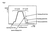
- the speed control means preferably provides at least a specific time period over which the relation V1 ⁇ V2 is satisfied, wherein V1 represents the speed at which the carrier film is taken up by the take-up means, and V2 represents the speed at which the sheet piece is bonded by the bonding means.
- the speed control means preferably controls the take-up means and the bonding means in such a manner that the take-up speed V1 and the bonding speed V2 are reduced before the intermediate time while kept equal to each other and that the relation V1 ⁇ V2 is satisfied from the intermediate time to the peeling-off end time.
- the peeling off can be finished at a lower speed, which makes it possible to further stabilize the peeling off and to further suppress the occurrence of stripe defects.
- the carrier film feeding means may have a dancer roller through which the carrier film is fed to the peeling means.
- the carrier film can be automatically shifted back to the upstream side after the peeling off is completed, so that the reset for the bonding of the next sheet piece of the polarizing film can be easily achieved.
- a method including placing a feed roller upstream of the peeling means and turning the feed roller against the normal direction of rotation may be used as the method for automatically shifting back the carrier film after the completion of the peeling off.
- the invention is also directed to a method for continuously manufacturing a liquid crystal display device, including: a carrier film feeding step including feeding a carrier film on which a sheet piece of a polarizing film is formed with a pressure-sensitive adhesive interposed therebetween; a peeling off step including peeling off the sheet piece of the polarizing film and the pressure-sensitive adhesive from the carrier film by using peeling means to inwardly fold back, at its front end, the carrier film fed by the carrier film feeding step; a take-up step including taking up the carrier film, from which the sheet piece is peeled off by the peeling off step, using take-up means; a bonding step including bonding the sheet piece, which is peeled off from the carrier film by the peeling off step, to a liquid crystal panel with the pressure-sensitive adhesive interposed therebetween using bonding means while feeding the liquid crystal panel so that a liquid crystal display device is formed; and a speed control step comprising controlling the take-up means and the bonding means in such a manner that the carrier film is folded back at the front end
- the carrier film is allowed to protrude from the front end of the peeling means as it is pulled by the sheet piece of the polarizing film being bonded to the liquid crystal panel, so that the timing of peeling off the rear part of the sheet piece of the polarizing film is delayed, which makes it possible to peel off the rear end of the sheet piece of the polarizing film after it is allowed to protrude from the front end of the peeling means toward the bonding site.
- the radius R1 of peel curvature at the position where the sheet piece of the polarizing film is peeled off can be made smaller than the radius R2 of peel curvature at the front end of the peeling means, so that the peel angle can be made smaller.
- the rear part of the sheet piece of the polarizing film can be stably peeled off from the carrier film at a smaller peel angle (typically, the polarizing film can be prevented from being swingingly displaced), when the sheet piece of the polarizing film is bonded to the liquid crystal panel, so that the occurrence of so-called stripe defects can be suppressed.
- At least a specific time period over which the relation VI ⁇ V2 is satisfied is preferably provided during the period from a bonding start time when bonding the sheet piece is started to the peeling-off end time of the sheet piece, wherein V1 represents the speed at which the carrier film is taken up by the take-up means, and V2 represents the speed at which the sheet piece is bonded by the bonding means.
- the advantageous effects of the invention can be easily obtained.
- the take-up means and the bonding means are preferably controlled in such a manner that the take-up speed V1 and the bonding speed V2 are reduced before the intermediate time while kept equal to each other and that the relation V1 ⁇ V2 is satisfied from the intermediate time to the peeling-off end time.
- the peeling off can be finished at a lower speed, which makes it possible to further stabilize the peeling off and to further suppress the occurrence of stripe defects.
- the carrier film feeding step may include feeding the carrier film to the peeling means through a dancer roller. According to this feature, the carrier film can be automatically shifted back to the upstream side after the peeling off is completed, so that the reset for the bonding of the next sheet piece of the polarizing film can be easily achieved.
- the polarizing film may be formed on the carrier film in any mode.
- they may be wound to form a continuous roll.
- the continuous roll may be (1) a roll of an optical film laminate including a carrier film and a polarizing film formed on the carrier film with a pressure-sensitive adhesive interposed therebetween.
- the system for continuously manufacturing a liquid crystal display device has cutting means for cutting the polarizing film into sheet pieces of the polarizing film in such a manner that the polarizing film and the pressure-sensitive adhesive are cut at predetermined intervals, while the carrier film is left uncut (cutting means for performing half-cutting).
- the cutting may be performed in such a manner as to classify non-defective and defective sheet pieces based on the result of an inspection performed using a defect inspection apparatus in the continuous manufacturing system.
- the continuous roll may be (2) a roll of an optical film laminate including a carrier film and sheet pieces of a polarizing film formed on the carrier film with a pressure-sensitive adhesive interposed therebetween (a continuous roll of a so-called scored polarizing film).
- the first continuous roll 1 shown in Fig. 1 is a roll of a first optical film laminate 11 including a first carrier film 12 and a first polarizing film 13 formed on the first carrier film 12 with a first pressure-sensitive adhesive interposed therebetween.
- the polarizing film includes a polarizer (about 5 to about 80 um in thickness) and a polarizer protecting film or films (generally about 1 to about 500 ⁇ m in thickness) formed on one or both sides of the polarizer with or without an adhesive.
- the first optical film laminate 11 may further include any other film such as a retardation film (generally 10 to 200 um in thickness), a viewing angle compensation film, a brightness enhancement film, or a surface protecting film.
- the thickness of the optical film laminate is typically in the range of 10 ⁇ m to 500 ⁇ m.
- the pressure-sensitive adhesive interposed between the polarizing film and the carrier film may be of any type such as an acryl-based pressure-sensitive adhesive, a silicone pressure-sensitive adhesive, or a urethane pressure-sensitive adhesive.
- the thickness of the pressure-sensitive adhesive is preferably in the range of 10 to 50 ⁇ m.
- the carrier film to be used may be such a known conventional film as a plastic film (e.g., a polyethylene terephthalate film or a polyolefin film).
- any appropriate film such as a film coated with an appropriate release agent such as a silicone, long-chain alkyl or fluoride release agent, or molybdenum sulfide may also be used as needed.
- the liquid crystal display device includes a liquid crystal panel and a sheet piece or pieces of a polarizing film provided on one or both sides of the liquid crystal panel, into which a driving circuit is incorporated as needed. Any type of liquid crystal panel such as a vertical alignment (VA) or in-plane switching (IPS) type liquid crystal panel may be used.
- the liquid crystal panel 4 shown in Fig. 1 has a structure including a pair of substrates (first and second substrates 41 and 42) opposed to each other and a liquid crystal layer sealed in between the substrates.
- the system for continuously manufacturing a liquid crystal display device includes: carrier film feeding means for feeding a carrier film on which a sheet piece of a polarizing film is formed with a pressure-sensitive adhesive interposed therebetween; peeling means for peeling off the sheet piece and the pressure-sensitive adhesive from the carrier film by inwardly folding back, at its front end, the carrier film fed by the carrier film feeding means; take-up means for taking up the carrier film from which the sheet piece is peeled off by the peeling means; and bonding means for bonding the sheet piece, which is peeled off from the carrier film by the peeling means, to a liquid crystal panel with the pressure-sensitive adhesive interposed therebetween while feeding the liquid crystal panel so that a liquid crystal display device can be formed.
- the system also includes speed control means for controlling the take-up means and the bonding means so that the carrier film can be folded back while it is allowed to protrude from the front end of the peeling means toward the bonding means at least at a peeling-off end time when peeling off the sheet piece from the carrier film is completed.
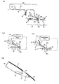
- the system for continuously manufacturing a liquid crystal display device includes first carrier film feeding means 101, first liquid crystal panel feeding means 102, first bonding means 103 (including a first bonding roller 50a and a first drive roller 50b), second liquid crystal panel feeding means 104, second carrier film feeding means, second bonding means (including a second bonding roller and a second drive roller), and liquid crystal display device feeding means.
- first sheet piece of a first polarizing film is bonded to a liquid crystal panel from the upper side, and then after the liquid crystal panel with the first sheet piece bonded thereto is turned over (upside down and optionally turned by 90°), a second sheet piece of a second polarizing film is bonded to the liquid crystal panel from the upper side.
- the first sheet piece may be bonded to the liquid crystal panel from the lower side, and then after the liquid crystal panel is turned over, the second sheet piece may be bonded to the liquid crystal panel from the lower side.
- the second sheet piece may be bonded to the liquid crystal panel from the lower side without turning over the liquid crystal panel, or after the first sheet piece is bonded to the liquid crystal panel from the lower side, the second sheet piece may be bonded to the liquid crystal panel from the upper side without turning over the liquid crystal panel.
- the first liquid crystal panel feeding means 102 transports and supplies the liquid crystal panel 4 to the first bonding means 103.
- the first liquid crystal panel feeding means 102 includes a feed roller 80, a suction plate, or the like.
- the liquid crystal panel 4 is fed to the downstream side of the manufacturing line by rotating the feed roller 80 or shifting the suction plate.
- the first carrier film feeding means 101 feeds the first optical film laminate 11 from the first continuous roll 1, cuts the first polarizing film and the pressure-sensitive adhesive at predetermined intervals to form a sheet piece 13 (first sheet piece) of the first polarizing film on the first carrier film 12, peels off the the first sheet piece 13 and the pressure-sensitive adhesive from the first carrier film 12 by inwardly folding back the first carrier film 12 at the front end of the first peeling means 40, and feeds the first sheet piece 13 and the pressure-sensitive adhesive to the first bonding means 103.
- the first carrier film feeding means 101 includes first cutting means 20, a first dancer roller 30, first peeling means 40, and first take-up means 60.
- the first cutting means 20 holds the first optical film laminate 11 from the first carrier film 12 side by suction means 21 and cuts the first polarizing film and the pressure-sensitive adhesive to form the first sheet piece 13 on the first carrier film 12.
- the first cutting means 20 may be a cutter, a laser, or the like.
- the first dancer roller 30 has the function of maintaining tension on the first carrier film 12 (absorbing fluctuations in tension).
- the first carrier film feeding means 101 feeds the first carrier film 12 through the first dancer roller 30.
- the first dancer roller 30 can function to allow the first carrier film 12 to protrude from the front end of the first peeling means 40. After peeling off the first sheet piece 13 from the first carrier film 12 is completed during the bonding process, the first dancer roller 30 also automatically shifts the first carrier film 12 back to the upstream side from the position ahead of the front end of the first peeling means 40.
- the first peeling means 40 In order to bond the first sheet piece 13 to the liquid crystal panel 4, the first peeling means 40 inwardly folds back the first carrier film 12 at its front end to peel off the first sheet piece 13 and the pressure-sensitive adhesive from the first carrier film 12.
- a sharp knife edge is used as a non-limiting example of the front end of the first peeling means 40.
- the sharp knife edge shown in Fig. 4 may have a radius R2 of curvature of 0.3 mm to 5.0 mm (corresponding to the radius of peel curvature).
- the first take-up means 60 takes up the first carrier film 12 from which the first sheet piece 13 and the pressure-sensitive adhesive are peeled off. During the process of bonding the first sheet piece 13, the speed V1 at which the first carrier film 12 is taken up by the first take-up means 60 is controlled by first speed control means 110 as described below.
- the first bonding means 103 bonds the first sheet piece 13 to the liquid crystal panel 4 from the upper side with the pressure-sensitive adhesive interposed therebetween, when the liquid crystal panel 4 and the first sheet piece 13 are fed by the first liquid crystal panel feeding means 102 and the first carrier film feeding means 101, respectively.
- the first bonding means 103 includes a first bonding roller 50a and and a first drive roller 50b.
- the speed of the rotation of the first drive roller 50b is controlled by the speed control means 110 described below. It has a mechanism in which as the first drive roller 50b is driven, the first bonding roller 50a is driven accordingly.
- Such a mechanism is non-limiting, and alternatively, the relationship between the driver and the follower may be reversed in the mechanism, or both may be drive mechanisms.
- the first speed control means 110 controls the first take-up means 60 and the first drive roller 50b synchronously so that the speed V1 at which the first carrier film 12 is taken up (feed speed) and the speed V2 at which the liquid crystal panel 4 is subjected to the bonding (feed speed) can be controlled during the process of bonding the first sheet piece 13 (see Figs. 2 and 3 ).
- the first speed control means 110 may control the first take-up means 60 of the first carrier film feeding means 101 so that the speed at which the first carrier film 12 is taken up (feed speed) can be controlled.
- a feed roller located downstream of the first peeling means 40 may be controlled so that the first carrier film 12 feed speed can be controlled.
- the first speed control means 110 may control the rotational speed of the first drive roller 50b so that the speed V2 at which the liquid crystal panel 4 is subjected to the bonding (feed speed) can be controlled.
- the first speed control means 110 controls the first take-up means 60 and the first drive roller 50b so that at least a specific time period over which the relation V1 ⁇ V2 is satisfied can be provided during the period from the bonding start time when bonding the polarizing film is started to the peeling-off end time when peeling off the first sheet piece 13 is completed.
- the first feed speed control means 110 makes the speed V1 at which the first carrier film 12 is taken up smaller than the speed V2 at which the liquid crystal panel 4 is subjected to the bonding (V1 ⁇ V2)
- the position where the first sheet piece 13 is peeled off (the position where the carrier film is folded back) is allowed to go ahead of the front end of the first peeling means 40 toward the position where the bonding is performed by the first bonding roller 50a
- the radius R1 of peel curvature at the position where the first sheet piece 13 allowed to go ahead is peeled off can be made smaller than the radius R2 of peel curvature at the front end of the first peeling means 40 in the process of peeling off the first sheet piece 13 and the pressure-sensitive adhesive from the first carrier film 12.
- the first speed control means 110 preferably controls the first take-up means 60 and the first drive roller 50b in such a manner that the take-up speed V1 and the bonding speed V2 are reduced before the speed changing time while kept equal to each other and that the relation V1 ⁇ V2 is satisfied from the speed changing time to the peeling-off end time. In this case, the peeling off is finished at a reduced speed, so that the peeling off can be further stabilized and that the occurrence of stripe defects can be further suppressed.
- the second liquid crystal panel feeding means 104 transports and supplies, to the second bonding means, the liquid crystal panel 4 with the first sheet piece 13 bonded thereto by the first bonding means 103.
- the second liquid crystal panel feeding means 104 includes a turning mechanism (not shown) for horizontally turning by 90° the liquid crystal panel 4 with the first sheet piece 13 bonded thereto and a turn-over mechanism for turning over the liquid crystal panel 4 with the first sheet piece 13 bonded thereto.
- the second carrier film feeding means may have the same device configuration as the first carrier film feeding means, and the second bonding means may have the same device configuration as the first bonding means.
- the second dancer roller may have the same device configuration as the first dancer roller 30
- the second take-up means may have the same device configuration as the first take-up means 60
- the second bonding roller and the second drive roller may have the same mechanism as the first bonding roller 50a and the first drive roller 50b.
- the second speed control means may also have the same function as the first speed control means.
- the liquid crystal display device feeding means may include a feed roller, a suction plate or any other component for feeding downstream the liquid crystal display device Y formed by the second bonding means.
- An inspection apparatus for inspecting the liquid crystal display device Y may also be provided at a downstream feed site. The purpose and method of the inspection with the inspection apparatus are not restricted.
- the method according to the embodiment for manufacturing a liquid crystal display device includes: a carrier film feeding step including feeding a carrier film on which a sheet piece of a polarizing film is formed with a pressure-sensitive adhesive interposed therebetween; a peeling off step including peeling off the sheet piece of the polarizing film and the pressure-sensitive adhesive from the carrier film by using peeling means to inwardly fold back, at its front end, the carrier film fed by the carrier film feeding step; a take-up step including taking up the carrier film, from which the sheet piece is peeled off by the peeling off step, using take-up means; a bonding step including bonding the sheet piece, which is peeled off from the carrier film by the peeling off step, to a liquid crystal panel with the pressure-sensitive adhesive interposed therebetween using bonding means while feeding the liquid crystal panel so that a liquid crystal display device is formed; and a speed control step including controlling the take-up means and the bonding means so that the carrier film can be folded back while it is allowed to protrude from the front
- the first bonding step includes bonding a first sheet piece of a first polarizing film to a first substrate of a liquid crystal panel, wherein the first polarizing film is fed from a first continuous roll.
- the first optical film laminate 11 is fed from the first continuous roll 1 which is a roll of the first optical film laminate 11 including the first carrier film 12 and the first polarizing film formed on the first carrier film 12.
- the first polarizing film and the pressure-sensitive adhesive are then cut while the first carrier film 12 is left (uncut), so that a first sheet piece 13 of the first polarizing film is formed on the first carrier film 12.
- the first carrier film 12 is then inwardly folded back at the front end of the first peeling means 40 and fed so that the first sheet piece 13 and the pressure-sensitive adhesive are peeled off from the first carrier film 12.
- the first sheet piece 13 peeled off from the first carrier film 12 is then bonded to the first substrate of the liquid crystal panel 4 with the pressure-sensitive adhesive interposed therebetween.
- the first speed control step includes controlling the first take-up means 60 and the first bonding means 103 so that the first carrier film 12 can be folded back while it is allowed to protrude from the front end of the first peeling means 40 toward the first bonding means 103 at least at the peeling-off end time when peeling off the first sheet piece 13 from the first carrier film 12 is completed.
- At least a specific time period over which the relation V1 ⁇ V2 is satisfied should be provided during the period from the bonding start time when bonding the first sheet piece 13 is started to the peeling-off end time when peeling off the first sheet piece 13 is completed, wherein V1 represents the speed at which the first carrier film 12 is taken up by the first take-up means 60, and V2 represents the speed at which the first sheet piece 13 of the first polarizing film is bonded by the first bonding means 103.
- the first speed control step preferably includes controlling the first take-up means 60 and the first bonding means 103 in such a manner that the take-up speed V1 and the bonding speed V2 are reduced before the intermediate time while kept equal to each other and that the relation V1 ⁇ V2 is satisfied from the intermediate time to the peeling-off end time.
- the carrier film feeding step includes feeding the carrier film in such a manner that tension on the carrier film can be maintained.
- the first dancer roller 30 is used to maintain tension on the first carrier film 12.
- the method should further include the step of turning and turning over the liquid crystal panel.
- the step of turning and turning over includes horizontally turning by 90° the liquid crystal panel 4 with the first polarizing film 14 bonded thereto and turning over the liquid crystal panel 4.
- the step of bonding a sheet piece of the second polarizing film may be performed in the same manner as the first bonding step, and the second speed control step may also be performed in the same manner as the first speed control step.
- the optical film laminate is fed from the continuous roll and cut at predetermined intervals.
- this feature is non-limiting.
- the optical film laminate fed from the continuous roll may be inspected for defects and cut in such a manner that defects are avoided based on the result of the inspection (by so-called skip cutting).
- defect information previously attached to the optical film laminate may be read out, and the optical film laminate may be cut in such a manner that defects are avoided based on the defect information.
- the first and second polarizing films in the first and second continuous rolls may also have previously undergone cutting.
- the first and second continuous rolls to be used may be so-called scored continuous rolls. In this case, the first and second cutting means are unnecessary, so that the tact time can be reduced.
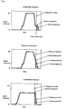
- a polarizing film was bonded to a liquid crystal panel (40 inches) from the long side using the manufacturing system shown in Fig. 1 under the speed conditions shown in Fig. 6 (Examples 1 to 3) or Fig. 7 (Comparative Examples 1 to 3).
- Example 1 included reducing both the take-up speed (V1: the carrier film feed speed) and the bonding speed (V2: the liquid crystal panel feed speed) from the maximum speed, then further reducing only the take-up speed (V1), and setting the bonding speed (V2) around the peeling-off end time at a constant speed.
- Example 2 included reducing the take-up speed (V1) and the bonding speed (V2) from the maximum speed while making a difference between them (V1 ⁇ V2) and setting the bonding speed (V2) around the peeling-off end time during the reduction in speed.
- Example 3 included reducing only the take-up speed (V1) from the maximum speed before the peeling-off end time and setting the bonding speed (V2) around the peeling-off end time at a constant speed.
- Comparative Example 1 included reducing both the take-up speed (V1) and the bonding speed (V2) from the maximum speed, then setting, at a constant speed, the bonding speed (V2) and the take-up speed (V1) around the peeling-off end time, and then reducing the take-up speed (V1) while keeping the bonding speed (V2) constant.
- Comparative Example 2 included reducing both the take-up speed (V1) and the bonding speed (V2) from the maximum speed and then, after the peeling-off end time, reducing the take-up speed (V1) and the bonding speed (V2) while making a difference between them (V1 ⁇ V2).
- Comparative Example 3 included reducing only the take-up speed (V1) from the maximum speed at the same time as the peeling-off end time and setting the bonding speed (V2) around the peeling-off end time at a constant speed.
- Example 1 shows that the stripe occurrence rate is lower in Examples 1 to 3 than in Comparative Examples 1 to 3.
- the result of Example 1 shows that the speed control process including reducing the take-up speed (V1) and the bonding speed (V2) from the maximum speed and then further reducing the carrier film take-up speed (V1) than the bonding speed (V2) while keeping the bonding speed (V2) constant until the peeling off is ended is more effective than the speed control processes in Examples 2 and 3.
Landscapes
- Physics & Mathematics (AREA)
- Nonlinear Science (AREA)
- General Physics & Mathematics (AREA)
- Optics & Photonics (AREA)
- Chemical & Material Sciences (AREA)
- Crystallography & Structural Chemistry (AREA)
- Engineering & Computer Science (AREA)
- Mathematical Physics (AREA)
- Mechanical Engineering (AREA)
- Manufacturing & Machinery (AREA)
- Liquid Crystal (AREA)
- Polarising Elements (AREA)
Claims (10)
- Système pour fabriquer en continu un dispositif d'affichage à cristaux liquides, comprenant :- des moyens d'alimentation en film de support (101) pour délivrer un film de support (12), sur lequel une pièce de feuille d'un film polarisant (13) est formée avec un adhésif sensible à la pression interposé entre eux, suivant une direction prédéterminée ;- des moyens de délaminage (40) pour détacher la pièce de feuille et l'adhésif sensible à la pression du film de support (12) délivré par les moyens d'alimentation en film de support (101), en repliant vers l'intérieur le film de support à l'extrémité avant des moyens de délaminage par rapport à ladite direction ;- des moyens de rattrapage (60) pour retendre le film de support (12) à partir duquel la pièce de feuille est détachée par les moyens de délaminage (40) ;- des moyens de collage (103) pour coller la pièce de feuille, qui est détachée du film de support (12) par les moyens de délaminage (40), sur un écran à cristaux liquides (4), avec l'adhésif sensible à la pression interposé entre eux, tout en délivrant l'écran à cristaux liquides (4) de telle sorte qu'un dispositif d'affichage à cristaux liquides puisse être formé ; et- des moyens de commande de vitesse (110) pour commander les moyens de rattrapage (60) et les moyens de collage (103) ;- caractérisé en ce que les moyens de commande de vitesse (110) sont adaptés à commander les moyens de rattrapage (60) et les moyens de collage (103) de telle manière que le film de support (12) soit replié à l'extrémité avant des moyens de délaminage (40) depuis un instant de commencement du collage, auquel le collage de la pièce de feuille est commencé, jusqu'à un instant intermédiaire et que le film de support (12) soit replié pendant qu'il est autorisé à dépasser de l'extrémité avant des moyens de délaminage (40) vers les moyens de collage (103) depuis l'instant intermédiaire jusqu'à un instant de fin de délaminage, auquel le détachement de la pièce de feuille du film de support (12) est terminé.
- Système selon la revendication 1, dans lequel les moyens de commande de vitesse (110) sont adaptés à commander les moyens de rattrapage (60) et les moyens de collage (103) de telle manière que la relation V1 < V2 soit satisfaite de l'instant intermédiaire à l'instant de fin de délaminage, V1 représentant la vitesse à laquelle le film de support (12) est retendu par les moyens de rattrapage (60) et V2 représentant la vitesse à laquelle la pièce de feuille est collée par les moyens de collage (103).
- Système selon la revendication 2, dans lequel les moyens de commande de vitesse (110) sont adaptés à commander les moyens de rattrapage (60) et les moyens de collage (103) de telle manière que la relation V1 = V2 soit satisfaite depuis l'instant de commencement du collage jusqu'à un instant intermédiaire antérieur à l'instant de fin de délaminage.
- Système selon la revendication 3, dans lequel les moyens de commande de vitesse (110) sont adaptés à commander les moyens de rattrapage (60) et les moyens de collage (103) de telle manière que la vitesse de rattrapage V1 et la vitesse de collage V2 soient réduites avant l'instant intermédiaire, tout en étant maintenues égales l'une à l'autre, et que la relation V1 < V2 soit satisfaite de l'instant intermédiaire à l'instant de fin de délaminage.
- Système selon la revendication 1, dans lequel les moyens d'alimentation en film de support (101) comportent un rouleau flottant par l'intermédiaire duquel le film de support (12) est délivré aux moyens de délaminage (40).
- Procédé pour fabriquer en continu un dispositif d'affichage à cristaux liquides, comprenant :- une étape d'alimentation en film de support consistant à délivrer un film de support (12), sur lequel une pièce de feuille d'un film polarisant (13) est formée avec un adhésif sensible à la pression interposé entre eux ;- une étape de délaminage consistant à détacher la pièce de feuille du film polarisant (13) et l'adhésif sensible à la pression du film de support (12) en utilisant des moyens de délaminage (40) pour replier vers l'intérieur, à son extrémité avant, le film de support (12) délivré par l'étape d'alimentation en film de support ;- une étape de rattrapage consistant à retendre le film de support (12), à partir duquel la pièce de feuille est détachée par l'étape de délaminage, en utilisant des moyens de rattrapage (60) ;- une étape de collage consistant à coller la pièce de feuille, qui est détachée du film de support (12) par l'étape de délaminage, sur un écran à cristaux liquides (4), avec l'adhésif sensible à la pression interposé entre eux, en utilisant des moyens de collage (103), tout en délivrant l'écran à cristaux liquides (4) de telle sorte qu'un dispositif d'affichage à cristaux liquides soit formé ; et- une étape de commande de vitesse consistant à commander les moyens de rattrapage (60) et les moyens de collage (103) ;- caractérisé en ce que les moyens de rattrapage (60) et les moyens de collage (103) sont commandés de telle manière que le film de support (12) soit replié à l'extrémité avant des moyens de délaminage (40) depuis un instant de commencement du collage, auquel le collage de la pièce de feuille est commencé, jusqu'à un instant intermédiaire et que le film de support (12) soit replié pendant qu'il est autorisé à dépasser de l'extrémité avant des moyens de délaminage (40) vers les moyens de collage (103) depuis l'instant intermédiaire jusqu'à un instant de fin de délaminage, auquel le détachement de la pièce de feuille du film de support (12) est terminé.
- Procédé selon la revendication 6, pour lequel, à l'étape de commande de vitesse, les moyens de rattrapage (60) et les moyens de collage (103) sont commandés de telle manière que la relation V1 < V2 soit satisfaite de l'instant intermédiaire à l'instant de fin de délaminage, V1 représentant la vitesse à laquelle le film de support (12) est retendu par les moyens de rattrapage (60) et V2 représentant la vitesse à laquelle la pièce de feuille est collée par les moyens de collage (103).
- Procédé selon la revendication 7, pour lequel, à l'étape de commande de vitesse, les moyens de rattrapage (60) et les moyens de collage (103) sont commandés de telle manière que la relation V1 = V2 soit satisfaite depuis l'instant de commencement du collage jusqu'à un instant intermédiaire antérieur à l'instant de fin de délaminage.
- Procédé selon la revendication 8, pour lequel, à l'étape de commande de vitesse, les moyens de rattrapage (60) et les moyens de collage (103) sont commandés de telle manière que la vitesse de rattrapage V1 et la vitesse de collage V2 soient réduites avant l'instant intermédiaire, tout en étant maintenues égales l'une à l'autre, et que la relation V1 < V2 soit satisfaite de l'instant intermédiaire à l'instant de fin de délaminage.
- Procédé selon la revendication 6, pour lequel l'étape d'alimentation en film de support inclut de délivrer le film de support (12) aux moyens de délaminage (40) par l'intermédiaire d'un rouleau flottant.
Priority Applications (1)
| Application Number | Priority Date | Filing Date | Title |
|---|---|---|---|
| PL11165389T PL2437101T3 (pl) | 2010-09-29 | 2011-05-10 | Układ i sposób ciągłego wytwarzania urządzeń wyświetlacza ciekłokrystalicznego |
Applications Claiming Priority (1)
| Application Number | Priority Date | Filing Date | Title |
|---|---|---|---|
| JP2010218238A JP4689763B1 (ja) | 2010-09-29 | 2010-09-29 | 液晶表示素子の連続製造システムおよび液晶表示素子の連続製造方法 |
Publications (2)
| Publication Number | Publication Date |
|---|---|
| EP2437101A1 EP2437101A1 (fr) | 2012-04-04 |
| EP2437101B1 true EP2437101B1 (fr) | 2012-11-07 |
Family
ID=44193914
Family Applications (1)
| Application Number | Title | Priority Date | Filing Date |
|---|---|---|---|
| EP11165389A Not-in-force EP2437101B1 (fr) | 2010-09-29 | 2011-05-10 | Procédé et système pour fabriquer en continu des dispositifs d'affichage à cristaux liquides |
Country Status (7)
| Country | Link |
|---|---|
| US (1) | US8128769B1 (fr) |
| EP (1) | EP2437101B1 (fr) |
| JP (1) | JP4689763B1 (fr) |
| KR (1) | KR101034111B1 (fr) |
| CN (1) | CN102419489B (fr) |
| PL (1) | PL2437101T3 (fr) |
| TW (1) | TW201213928A (fr) |
Families Citing this family (14)
| Publication number | Priority date | Publication date | Assignee | Title |
|---|---|---|---|---|
| JP4750227B1 (ja) * | 2011-01-14 | 2011-08-17 | 日東電工株式会社 | 液晶表示素子の連続製造システムおよび液晶表示素子の連続製造方法 |
| JP5868734B2 (ja) * | 2012-03-06 | 2016-02-24 | 日東電工株式会社 | 光学表示パネルの連続製造方法および光学表示パネルの連続製造システム |
| JP5868733B2 (ja) * | 2012-03-06 | 2016-02-24 | 日東電工株式会社 | 光学表示パネルの連続製造方法および光学表示パネルの連続製造システム |
| JP6101431B2 (ja) * | 2012-04-16 | 2017-03-22 | 日東電工株式会社 | 光学表示パネルの連続製造方法および光学表示パネルの連続製造システム |
| JP5427929B2 (ja) * | 2012-08-10 | 2014-02-26 | 日東電工株式会社 | 光学表示パネルの連続製造方法及び光学表示パネルの連続製造システム |
| JP6115334B2 (ja) * | 2013-06-07 | 2017-04-19 | 三菱電機株式会社 | 表示装置の製造方法および製造装置 |
| JP2016130860A (ja) * | 2016-02-10 | 2016-07-21 | 日東電工株式会社 | 光学表示パネルの連続製造方法および光学表示パネルの連続製造システム |
| JP6171041B1 (ja) * | 2016-04-06 | 2017-07-26 | 日東電工株式会社 | 光学的表示装置を製造する方法 |
| KR101678803B1 (ko) | 2016-06-03 | 2016-11-22 | 주식회사 엘지화학 | 광학 표시 소자의 연속 제조 시스템 및 방법 |
| JP6651588B2 (ja) * | 2017-10-05 | 2020-02-19 | 日東電工株式会社 | 樹脂フィルム貼り付けのためシステム及び方法 |
| CN108340591A (zh) * | 2018-01-22 | 2018-07-31 | 王海彬 | 一种防水膜的现场贴附机械 |
| CN112277432B (zh) * | 2020-10-28 | 2023-12-19 | 京东方科技集团股份有限公司 | 一种保护膜剥离系统及其控制方法、保护膜剥离方法 |
| CN113459176B (zh) * | 2021-08-05 | 2025-03-07 | 四川展新胶粘材料有限公司 | 防止反离型的剥离设备 |
| CN114084733B (zh) * | 2022-01-07 | 2022-05-03 | 江苏国沃纺织品有限公司 | 一种基于物联网的纺织品智能生产分离装置 |
Family Cites Families (13)
| Publication number | Priority date | Publication date | Assignee | Title |
|---|---|---|---|---|
| JPS5752017A (en) | 1980-08-08 | 1982-03-27 | Sharp Corp | Tacky-polarizing-plate defective removing device automatic tacky-polarizing-plate sticking machine |
| JP2002127258A (ja) * | 2000-10-24 | 2002-05-08 | Mck:Kk | シート部材の貼り合わせ装置 |
| KR20040002796A (ko) * | 2002-06-28 | 2004-01-07 | 후지 샤신 필름 가부시기가이샤 | 편광판 점착방법 및 그 장치 |
| JP3989354B2 (ja) * | 2002-10-11 | 2007-10-10 | リンテック株式会社 | 貼合装置 |
| JP4124022B2 (ja) * | 2003-01-23 | 2008-07-23 | ソニー株式会社 | 貼り合わせ装置および貼り合わせ方法 |
| JP2004338408A (ja) * | 2003-04-24 | 2004-12-02 | Mitsui Chemicals Inc | フィルムのラミネート方法および装置 |
| JP4371709B2 (ja) | 2003-06-05 | 2009-11-25 | 富士フイルム株式会社 | 光学フィルム貼付装置及び方法 |
| KR101012799B1 (ko) | 2004-02-06 | 2011-02-08 | 삼성전자주식회사 | 액정 표시 장치의 제조 시스템 및 이를 이용한 제조 방법 |
| JP4255433B2 (ja) * | 2004-03-15 | 2009-04-15 | 日東電工株式会社 | 枚葉体の貼合せ方法およびこれを用いた装置 |
| CN102837437B (zh) * | 2006-10-17 | 2015-02-18 | 日东电工株式会社 | 光学部件贴合方法以及使用该方法的装置 |
| WO2009128115A1 (fr) | 2008-04-15 | 2009-10-22 | 日東電工株式会社 | Rouleau stratifié de film optique, et son procédé et dispositif de fabrication |
| JP4785944B2 (ja) * | 2008-04-16 | 2011-10-05 | 日東電工株式会社 | 光学表示装置の製造方法 |
| JP5311277B2 (ja) | 2008-07-29 | 2013-10-09 | 日本電気硝子株式会社 | 板状ワークの移送設備および移送方法 |
-
2010
- 2010-09-29 JP JP2010218238A patent/JP4689763B1/ja active Active
- 2010-11-02 TW TW099137669A patent/TW201213928A/zh unknown
-
2011
- 2011-01-17 KR KR1020110004602A patent/KR101034111B1/ko active Active
- 2011-04-07 US US13/081,610 patent/US8128769B1/en not_active Expired - Fee Related
- 2011-04-08 CN CN2011100910126A patent/CN102419489B/zh active Active
- 2011-05-10 EP EP11165389A patent/EP2437101B1/fr not_active Not-in-force
- 2011-05-10 PL PL11165389T patent/PL2437101T3/pl unknown
Also Published As
| Publication number | Publication date |
|---|---|
| US20120073742A1 (en) | 2012-03-29 |
| TWI360679B (fr) | 2012-03-21 |
| JP4689763B1 (ja) | 2011-05-25 |
| TW201213928A (en) | 2012-04-01 |
| KR101034111B1 (ko) | 2011-05-13 |
| US8128769B1 (en) | 2012-03-06 |
| CN102419489B (zh) | 2013-04-03 |
| PL2437101T3 (pl) | 2013-04-30 |
| EP2437101A1 (fr) | 2012-04-04 |
| JP2012073423A (ja) | 2012-04-12 |
| CN102419489A (zh) | 2012-04-18 |
Similar Documents
| Publication | Publication Date | Title |
|---|---|---|
| EP2437101B1 (fr) | Procédé et système pour fabriquer en continu des dispositifs d'affichage à cristaux liquides | |
| US8888937B2 (en) | Method for continuously manufacturing liquid crystal display device | |
| US9283739B2 (en) | Method and system for continuously manufacturing optical display panel | |
| US9151982B2 (en) | Manufacturing system and manufacturing method for optical display device | |
| KR101717830B1 (ko) | 광학 표시 패널의 연속 제조 방법 및 광학 표시 패널의 연속 제조 시스템 | |
| US10710351B2 (en) | System and method for continuously manufacturing optical display device | |
| US9561641B2 (en) | Method and system for continuously manufacturing optical display panel | |
| US8485241B2 (en) | System and method for continuously manufacturing liquid crystal display device | |
| KR101774631B1 (ko) | 광학 표시 패널의 연속 제조 방법 및 광학 표시 패널의 연속 제조 시스템 | |
| JP6088187B2 (ja) | 光学表示パネルの連続製造方法及び光学表示パネルの連続製造システム | |
| US20120097325A1 (en) | System and method for continuously manufacturing liquid crystal display device | |
| JP2016130860A (ja) | 光学表示パネルの連続製造方法および光学表示パネルの連続製造システム |
Legal Events
| Date | Code | Title | Description |
|---|---|---|---|
| PUAI | Public reference made under article 153(3) epc to a published international application that has entered the european phase |
Free format text: ORIGINAL CODE: 0009012 |
|
| 17P | Request for examination filed |
Effective date: 20111109 |
|
| AK | Designated contracting states |
Kind code of ref document: A1 Designated state(s): AL AT BE BG CH CY CZ DE DK EE ES FI FR GB GR HR HU IE IS IT LI LT LU LV MC MK MT NL NO PL PT RO RS SE SI SK SM TR |
|
| AX | Request for extension of the european patent |
Extension state: BA ME |
|
| REG | Reference to a national code |
Ref country code: DE Ref legal event code: R079 Ref document number: 602011000409 Country of ref document: DE Free format text: PREVIOUS MAIN CLASS: G02F0001133300 Ipc: B29C0063000000 |
|
| GRAP | Despatch of communication of intention to grant a patent |
Free format text: ORIGINAL CODE: EPIDOSNIGR1 |
|
| RIC1 | Information provided on ipc code assigned before grant |
Ipc: G02F 1/1333 20060101ALI20120413BHEP Ipc: B29C 63/00 20060101AFI20120413BHEP |
|
| GRAS | Grant fee paid |
Free format text: ORIGINAL CODE: EPIDOSNIGR3 |
|
| GRAA | (expected) grant |
Free format text: ORIGINAL CODE: 0009210 |
|
| AK | Designated contracting states |
Kind code of ref document: B1 Designated state(s): AL AT BE BG CH CY CZ DE DK EE ES FI FR GB GR HR HU IE IS IT LI LT LU LV MC MK MT NL NO PL PT RO RS SE SI SK SM TR |
|
| REG | Reference to a national code |
Ref country code: GB Ref legal event code: FG4D |
|
| REG | Reference to a national code |
Ref country code: AT Ref legal event code: REF Ref document number: 582804 Country of ref document: AT Kind code of ref document: T Effective date: 20121115 Ref country code: CH Ref legal event code: EP |
|
| REG | Reference to a national code |
Ref country code: IE Ref legal event code: FG4D |
|
| REG | Reference to a national code |
Ref country code: DE Ref legal event code: R096 Ref document number: 602011000409 Country of ref document: DE Effective date: 20130103 |
|
| REG | Reference to a national code |
Ref country code: AT Ref legal event code: MK05 Ref document number: 582804 Country of ref document: AT Kind code of ref document: T Effective date: 20121107 |
|
| REG | Reference to a national code |
Ref country code: SK Ref legal event code: T3 Ref document number: E 13405 Country of ref document: SK |
|
| REG | Reference to a national code |
Ref country code: NL Ref legal event code: VDEP Effective date: 20121107 |
|
| REG | Reference to a national code |
Ref country code: LT Ref legal event code: MG4D |
|
| PG25 | Lapsed in a contracting state [announced via postgrant information from national office to epo] |
Ref country code: NO Free format text: LAPSE BECAUSE OF FAILURE TO SUBMIT A TRANSLATION OF THE DESCRIPTION OR TO PAY THE FEE WITHIN THE PRESCRIBED TIME-LIMIT Effective date: 20130207 Ref country code: LT Free format text: LAPSE BECAUSE OF FAILURE TO SUBMIT A TRANSLATION OF THE DESCRIPTION OR TO PAY THE FEE WITHIN THE PRESCRIBED TIME-LIMIT Effective date: 20121107 Ref country code: FI Free format text: LAPSE BECAUSE OF FAILURE TO SUBMIT A TRANSLATION OF THE DESCRIPTION OR TO PAY THE FEE WITHIN THE PRESCRIBED TIME-LIMIT Effective date: 20121107 Ref country code: IS Free format text: LAPSE BECAUSE OF FAILURE TO SUBMIT A TRANSLATION OF THE DESCRIPTION OR TO PAY THE FEE WITHIN THE PRESCRIBED TIME-LIMIT Effective date: 20130307 Ref country code: NL Free format text: LAPSE BECAUSE OF FAILURE TO SUBMIT A TRANSLATION OF THE DESCRIPTION OR TO PAY THE FEE WITHIN THE PRESCRIBED TIME-LIMIT Effective date: 20121107 Ref country code: SE Free format text: LAPSE BECAUSE OF FAILURE TO SUBMIT A TRANSLATION OF THE DESCRIPTION OR TO PAY THE FEE WITHIN THE PRESCRIBED TIME-LIMIT Effective date: 20121107 Ref country code: HR Free format text: LAPSE BECAUSE OF FAILURE TO SUBMIT A TRANSLATION OF THE DESCRIPTION OR TO PAY THE FEE WITHIN THE PRESCRIBED TIME-LIMIT Effective date: 20121107 Ref country code: ES Free format text: LAPSE BECAUSE OF FAILURE TO SUBMIT A TRANSLATION OF THE DESCRIPTION OR TO PAY THE FEE WITHIN THE PRESCRIBED TIME-LIMIT Effective date: 20130218 |
|
| REG | Reference to a national code |
Ref country code: PL Ref legal event code: T3 |
|
| PG25 | Lapsed in a contracting state [announced via postgrant information from national office to epo] |
Ref country code: BE Free format text: LAPSE BECAUSE OF FAILURE TO SUBMIT A TRANSLATION OF THE DESCRIPTION OR TO PAY THE FEE WITHIN THE PRESCRIBED TIME-LIMIT Effective date: 20121107 Ref country code: GR Free format text: LAPSE BECAUSE OF FAILURE TO SUBMIT A TRANSLATION OF THE DESCRIPTION OR TO PAY THE FEE WITHIN THE PRESCRIBED TIME-LIMIT Effective date: 20130208 Ref country code: LV Free format text: LAPSE BECAUSE OF FAILURE TO SUBMIT A TRANSLATION OF THE DESCRIPTION OR TO PAY THE FEE WITHIN THE PRESCRIBED TIME-LIMIT Effective date: 20121107 Ref country code: PT Free format text: LAPSE BECAUSE OF FAILURE TO SUBMIT A TRANSLATION OF THE DESCRIPTION OR TO PAY THE FEE WITHIN THE PRESCRIBED TIME-LIMIT Effective date: 20130307 Ref country code: SI Free format text: LAPSE BECAUSE OF FAILURE TO SUBMIT A TRANSLATION OF THE DESCRIPTION OR TO PAY THE FEE WITHIN THE PRESCRIBED TIME-LIMIT Effective date: 20121107 |
|
| PG25 | Lapsed in a contracting state [announced via postgrant information from national office to epo] |
Ref country code: AT Free format text: LAPSE BECAUSE OF FAILURE TO SUBMIT A TRANSLATION OF THE DESCRIPTION OR TO PAY THE FEE WITHIN THE PRESCRIBED TIME-LIMIT Effective date: 20121107 |
|
| PG25 | Lapsed in a contracting state [announced via postgrant information from national office to epo] |
Ref country code: DK Free format text: LAPSE BECAUSE OF FAILURE TO SUBMIT A TRANSLATION OF THE DESCRIPTION OR TO PAY THE FEE WITHIN THE PRESCRIBED TIME-LIMIT Effective date: 20121107 Ref country code: RS Free format text: LAPSE BECAUSE OF FAILURE TO SUBMIT A TRANSLATION OF THE DESCRIPTION OR TO PAY THE FEE WITHIN THE PRESCRIBED TIME-LIMIT Effective date: 20121107 Ref country code: EE Free format text: LAPSE BECAUSE OF FAILURE TO SUBMIT A TRANSLATION OF THE DESCRIPTION OR TO PAY THE FEE WITHIN THE PRESCRIBED TIME-LIMIT Effective date: 20121107 Ref country code: BG Free format text: LAPSE BECAUSE OF FAILURE TO SUBMIT A TRANSLATION OF THE DESCRIPTION OR TO PAY THE FEE WITHIN THE PRESCRIBED TIME-LIMIT Effective date: 20130207 |
|
| PG25 | Lapsed in a contracting state [announced via postgrant information from national office to epo] |
Ref country code: IT Free format text: LAPSE BECAUSE OF FAILURE TO SUBMIT A TRANSLATION OF THE DESCRIPTION OR TO PAY THE FEE WITHIN THE PRESCRIBED TIME-LIMIT Effective date: 20121107 Ref country code: RO Free format text: LAPSE BECAUSE OF FAILURE TO SUBMIT A TRANSLATION OF THE DESCRIPTION OR TO PAY THE FEE WITHIN THE PRESCRIBED TIME-LIMIT Effective date: 20121107 |
|
| PLBE | No opposition filed within time limit |
Free format text: ORIGINAL CODE: 0009261 |
|
| STAA | Information on the status of an ep patent application or granted ep patent |
Free format text: STATUS: NO OPPOSITION FILED WITHIN TIME LIMIT |
|
| 26N | No opposition filed |
Effective date: 20130808 |
|
| PG25 | Lapsed in a contracting state [announced via postgrant information from national office to epo] |
Ref country code: CY Free format text: LAPSE BECAUSE OF FAILURE TO SUBMIT A TRANSLATION OF THE DESCRIPTION OR TO PAY THE FEE WITHIN THE PRESCRIBED TIME-LIMIT Effective date: 20121107 |
|
| REG | Reference to a national code |
Ref country code: DE Ref legal event code: R097 Ref document number: 602011000409 Country of ref document: DE Effective date: 20130808 |
|
| PG25 | Lapsed in a contracting state [announced via postgrant information from national office to epo] |
Ref country code: MC Free format text: LAPSE BECAUSE OF FAILURE TO SUBMIT A TRANSLATION OF THE DESCRIPTION OR TO PAY THE FEE WITHIN THE PRESCRIBED TIME-LIMIT Effective date: 20121107 |
|
| REG | Reference to a national code |
Ref country code: IE Ref legal event code: MM4A |
|
| PG25 | Lapsed in a contracting state [announced via postgrant information from national office to epo] |
Ref country code: IE Free format text: LAPSE BECAUSE OF NON-PAYMENT OF DUE FEES Effective date: 20130510 |
|
| REG | Reference to a national code |
Ref country code: CH Ref legal event code: PL |
|
| PG25 | Lapsed in a contracting state [announced via postgrant information from national office to epo] |
Ref country code: CH Free format text: LAPSE BECAUSE OF NON-PAYMENT OF DUE FEES Effective date: 20140531 Ref country code: LI Free format text: LAPSE BECAUSE OF NON-PAYMENT OF DUE FEES Effective date: 20140531 |
|
| PG25 | Lapsed in a contracting state [announced via postgrant information from national office to epo] |
Ref country code: MT Free format text: LAPSE BECAUSE OF FAILURE TO SUBMIT A TRANSLATION OF THE DESCRIPTION OR TO PAY THE FEE WITHIN THE PRESCRIBED TIME-LIMIT Effective date: 20121107 |
|
| PG25 | Lapsed in a contracting state [announced via postgrant information from national office to epo] |
Ref country code: SM Free format text: LAPSE BECAUSE OF FAILURE TO SUBMIT A TRANSLATION OF THE DESCRIPTION OR TO PAY THE FEE WITHIN THE PRESCRIBED TIME-LIMIT Effective date: 20121107 |
|
| PG25 | Lapsed in a contracting state [announced via postgrant information from national office to epo] |
Ref country code: TR Free format text: LAPSE BECAUSE OF FAILURE TO SUBMIT A TRANSLATION OF THE DESCRIPTION OR TO PAY THE FEE WITHIN THE PRESCRIBED TIME-LIMIT Effective date: 20121107 |
|
| PG25 | Lapsed in a contracting state [announced via postgrant information from national office to epo] |
Ref country code: MK Free format text: LAPSE BECAUSE OF FAILURE TO SUBMIT A TRANSLATION OF THE DESCRIPTION OR TO PAY THE FEE WITHIN THE PRESCRIBED TIME-LIMIT Effective date: 20121107 Ref country code: HU Free format text: LAPSE BECAUSE OF FAILURE TO SUBMIT A TRANSLATION OF THE DESCRIPTION OR TO PAY THE FEE WITHIN THE PRESCRIBED TIME-LIMIT; INVALID AB INITIO Effective date: 20110510 Ref country code: LU Free format text: LAPSE BECAUSE OF NON-PAYMENT OF DUE FEES Effective date: 20130510 |
|
| REG | Reference to a national code |
Ref country code: FR Ref legal event code: PLFP Year of fee payment: 6 |
|
| REG | Reference to a national code |
Ref country code: FR Ref legal event code: PLFP Year of fee payment: 7 |
|
| REG | Reference to a national code |
Ref country code: FR Ref legal event code: PLFP Year of fee payment: 8 |
|
| PGFP | Annual fee paid to national office [announced via postgrant information from national office to epo] |
Ref country code: GB Payment date: 20180329 Year of fee payment: 8 |
|
| PGFP | Annual fee paid to national office [announced via postgrant information from national office to epo] |
Ref country code: SK Payment date: 20180416 Year of fee payment: 8 Ref country code: DE Payment date: 20180424 Year of fee payment: 8 Ref country code: CZ Payment date: 20180417 Year of fee payment: 8 |
|
| PGFP | Annual fee paid to national office [announced via postgrant information from national office to epo] |
Ref country code: FR Payment date: 20180412 Year of fee payment: 8 Ref country code: PL Payment date: 20180411 Year of fee payment: 8 |
|
| PG25 | Lapsed in a contracting state [announced via postgrant information from national office to epo] |
Ref country code: AL Free format text: LAPSE BECAUSE OF FAILURE TO SUBMIT A TRANSLATION OF THE DESCRIPTION OR TO PAY THE FEE WITHIN THE PRESCRIBED TIME-LIMIT Effective date: 20121107 |
|
| REG | Reference to a national code |
Ref country code: DE Ref legal event code: R119 Ref document number: 602011000409 Country of ref document: DE |
|
| GBPC | Gb: european patent ceased through non-payment of renewal fee |
Effective date: 20190510 |
|
| PG25 | Lapsed in a contracting state [announced via postgrant information from national office to epo] |
Ref country code: CZ Free format text: LAPSE BECAUSE OF NON-PAYMENT OF DUE FEES Effective date: 20190510 Ref country code: SK Free format text: LAPSE BECAUSE OF NON-PAYMENT OF DUE FEES Effective date: 20190510 |
|
| REG | Reference to a national code |
Ref country code: SK Ref legal event code: MM4A Ref document number: E 13405 Country of ref document: SK Effective date: 20190510 |
|
| PG25 | Lapsed in a contracting state [announced via postgrant information from national office to epo] |
Ref country code: DE Free format text: LAPSE BECAUSE OF NON-PAYMENT OF DUE FEES Effective date: 20191203 Ref country code: GB Free format text: LAPSE BECAUSE OF NON-PAYMENT OF DUE FEES Effective date: 20190510 |
|
| PG25 | Lapsed in a contracting state [announced via postgrant information from national office to epo] |
Ref country code: FR Free format text: LAPSE BECAUSE OF NON-PAYMENT OF DUE FEES Effective date: 20190531 |
|
| PG25 | Lapsed in a contracting state [announced via postgrant information from national office to epo] |
Ref country code: PL Free format text: LAPSE BECAUSE OF NON-PAYMENT OF DUE FEES Effective date: 20190510 |