EP2434531B1 - Procédé de fabrication pour un condensateur métal-isolant-métal - Google Patents
Procédé de fabrication pour un condensateur métal-isolant-métal Download PDFInfo
- Publication number
- EP2434531B1 EP2434531B1 EP11182813.3A EP11182813A EP2434531B1 EP 2434531 B1 EP2434531 B1 EP 2434531B1 EP 11182813 A EP11182813 A EP 11182813A EP 2434531 B1 EP2434531 B1 EP 2434531B1
- Authority
- EP
- European Patent Office
- Prior art keywords
- layer
- layers
- stack
- tio
- sto
- Prior art date
- Legal status (The legal status is an assumption and is not a legal conclusion. Google has not performed a legal analysis and makes no representation as to the accuracy of the status listed.)
- Active
Links
Images


Classifications
-
- H—ELECTRICITY
- H01—ELECTRIC ELEMENTS
- H01L—SEMICONDUCTOR DEVICES NOT COVERED BY CLASS H10
- H01L21/00—Processes or apparatus adapted for the manufacture or treatment of semiconductor or solid state devices or of parts thereof
- H01L21/02—Manufacture or treatment of semiconductor devices or of parts thereof
- H01L21/02104—Forming layers
- H01L21/02107—Forming insulating materials on a substrate
- H01L21/02296—Forming insulating materials on a substrate characterised by the treatment performed before or after the formation of the layer
- H01L21/02318—Forming insulating materials on a substrate characterised by the treatment performed before or after the formation of the layer post-treatment
- H01L21/02356—Forming insulating materials on a substrate characterised by the treatment performed before or after the formation of the layer post-treatment treatment to change the morphology of the insulating layer, e.g. transformation of an amorphous layer into a crystalline layer
-
- C—CHEMISTRY; METALLURGY
- C23—COATING METALLIC MATERIAL; COATING MATERIAL WITH METALLIC MATERIAL; CHEMICAL SURFACE TREATMENT; DIFFUSION TREATMENT OF METALLIC MATERIAL; COATING BY VACUUM EVAPORATION, BY SPUTTERING, BY ION IMPLANTATION OR BY CHEMICAL VAPOUR DEPOSITION, IN GENERAL; INHIBITING CORROSION OF METALLIC MATERIAL OR INCRUSTATION IN GENERAL
- C23C—COATING METALLIC MATERIAL; COATING MATERIAL WITH METALLIC MATERIAL; SURFACE TREATMENT OF METALLIC MATERIAL BY DIFFUSION INTO THE SURFACE, BY CHEMICAL CONVERSION OR SUBSTITUTION; COATING BY VACUUM EVAPORATION, BY SPUTTERING, BY ION IMPLANTATION OR BY CHEMICAL VAPOUR DEPOSITION, IN GENERAL
- C23C16/00—Chemical coating by decomposition of gaseous compounds, without leaving reaction products of surface material in the coating, i.e. chemical vapour deposition [CVD] processes
- C23C16/22—Chemical coating by decomposition of gaseous compounds, without leaving reaction products of surface material in the coating, i.e. chemical vapour deposition [CVD] processes characterised by the deposition of inorganic material, other than metallic material
- C23C16/30—Deposition of compounds, mixtures or solid solutions, e.g. borides, carbides, nitrides
- C23C16/40—Oxides
- C23C16/409—Oxides of the type ABO3 with A representing alkali, alkaline earth metal or lead and B representing a refractory metal, nickel, scandium or a lanthanide
-
- C—CHEMISTRY; METALLURGY
- C23—COATING METALLIC MATERIAL; COATING MATERIAL WITH METALLIC MATERIAL; CHEMICAL SURFACE TREATMENT; DIFFUSION TREATMENT OF METALLIC MATERIAL; COATING BY VACUUM EVAPORATION, BY SPUTTERING, BY ION IMPLANTATION OR BY CHEMICAL VAPOUR DEPOSITION, IN GENERAL; INHIBITING CORROSION OF METALLIC MATERIAL OR INCRUSTATION IN GENERAL
- C23C—COATING METALLIC MATERIAL; COATING MATERIAL WITH METALLIC MATERIAL; SURFACE TREATMENT OF METALLIC MATERIAL BY DIFFUSION INTO THE SURFACE, BY CHEMICAL CONVERSION OR SUBSTITUTION; COATING BY VACUUM EVAPORATION, BY SPUTTERING, BY ION IMPLANTATION OR BY CHEMICAL VAPOUR DEPOSITION, IN GENERAL
- C23C16/00—Chemical coating by decomposition of gaseous compounds, without leaving reaction products of surface material in the coating, i.e. chemical vapour deposition [CVD] processes
- C23C16/44—Chemical coating by decomposition of gaseous compounds, without leaving reaction products of surface material in the coating, i.e. chemical vapour deposition [CVD] processes characterised by the method of coating
- C23C16/455—Chemical coating by decomposition of gaseous compounds, without leaving reaction products of surface material in the coating, i.e. chemical vapour deposition [CVD] processes characterised by the method of coating characterised by the method used for introducing gases into reaction chamber or for modifying gas flows in reaction chamber
- C23C16/45523—Pulsed gas flow or change of composition over time
- C23C16/45525—Atomic layer deposition [ALD]
- C23C16/45527—Atomic layer deposition [ALD] characterized by the ALD cycle, e.g. different flows or temperatures during half-reactions, unusual pulsing sequence, use of precursor mixtures or auxiliary reactants or activations
- C23C16/45529—Atomic layer deposition [ALD] characterized by the ALD cycle, e.g. different flows or temperatures during half-reactions, unusual pulsing sequence, use of precursor mixtures or auxiliary reactants or activations specially adapted for making a layer stack of alternating different compositions or gradient compositions
-
- H—ELECTRICITY
- H01—ELECTRIC ELEMENTS
- H01L—SEMICONDUCTOR DEVICES NOT COVERED BY CLASS H10
- H01L21/00—Processes or apparatus adapted for the manufacture or treatment of semiconductor or solid state devices or of parts thereof
- H01L21/02—Manufacture or treatment of semiconductor devices or of parts thereof
- H01L21/02104—Forming layers
- H01L21/02107—Forming insulating materials on a substrate
- H01L21/02109—Forming insulating materials on a substrate characterised by the type of layer, e.g. type of material, porous/non-porous, pre-cursors, mixtures or laminates
- H01L21/02112—Forming insulating materials on a substrate characterised by the type of layer, e.g. type of material, porous/non-porous, pre-cursors, mixtures or laminates characterised by the material of the layer
- H01L21/02172—Forming insulating materials on a substrate characterised by the type of layer, e.g. type of material, porous/non-porous, pre-cursors, mixtures or laminates characterised by the material of the layer the material containing at least one metal element, e.g. metal oxides, metal nitrides, metal oxynitrides or metal carbides
- H01L21/02197—Forming insulating materials on a substrate characterised by the type of layer, e.g. type of material, porous/non-porous, pre-cursors, mixtures or laminates characterised by the material of the layer the material containing at least one metal element, e.g. metal oxides, metal nitrides, metal oxynitrides or metal carbides the material having a perovskite structure, e.g. BaTiO3
-
- H—ELECTRICITY
- H01—ELECTRIC ELEMENTS
- H01L—SEMICONDUCTOR DEVICES NOT COVERED BY CLASS H10
- H01L21/00—Processes or apparatus adapted for the manufacture or treatment of semiconductor or solid state devices or of parts thereof
- H01L21/02—Manufacture or treatment of semiconductor devices or of parts thereof
- H01L21/02104—Forming layers
- H01L21/02107—Forming insulating materials on a substrate
- H01L21/02225—Forming insulating materials on a substrate characterised by the process for the formation of the insulating layer
- H01L21/0226—Forming insulating materials on a substrate characterised by the process for the formation of the insulating layer formation by a deposition process
- H01L21/02263—Forming insulating materials on a substrate characterised by the process for the formation of the insulating layer formation by a deposition process deposition from the gas or vapour phase
- H01L21/02271—Forming insulating materials on a substrate characterised by the process for the formation of the insulating layer formation by a deposition process deposition from the gas or vapour phase deposition by decomposition or reaction of gaseous or vapour phase compounds, i.e. chemical vapour deposition
- H01L21/0228—Forming insulating materials on a substrate characterised by the process for the formation of the insulating layer formation by a deposition process deposition from the gas or vapour phase deposition by decomposition or reaction of gaseous or vapour phase compounds, i.e. chemical vapour deposition deposition by cyclic CVD, e.g. ALD, ALE, pulsed CVD
-
- H—ELECTRICITY
- H01—ELECTRIC ELEMENTS
- H01L—SEMICONDUCTOR DEVICES NOT COVERED BY CLASS H10
- H01L21/00—Processes or apparatus adapted for the manufacture or treatment of semiconductor or solid state devices or of parts thereof
- H01L21/02—Manufacture or treatment of semiconductor devices or of parts thereof
- H01L21/02104—Forming layers
- H01L21/02107—Forming insulating materials on a substrate
- H01L21/02296—Forming insulating materials on a substrate characterised by the treatment performed before or after the formation of the layer
- H01L21/02299—Forming insulating materials on a substrate characterised by the treatment performed before or after the formation of the layer pre-treatment
- H01L21/02304—Forming insulating materials on a substrate characterised by the treatment performed before or after the formation of the layer pre-treatment formation of intermediate layers, e.g. buffer layers, layers to improve adhesion, lattice match or diffusion barriers
-
- H—ELECTRICITY
- H01—ELECTRIC ELEMENTS
- H01L—SEMICONDUCTOR DEVICES NOT COVERED BY CLASS H10
- H01L28/00—Passive two-terminal components without a potential-jump or surface barrier for integrated circuits; Details thereof; Multistep manufacturing processes therefor
- H01L28/40—Capacitors
- H01L28/55—Capacitors with a dielectric comprising a perovskite structure material
- H01L28/56—Capacitors with a dielectric comprising a perovskite structure material the dielectric comprising two or more layers, e.g. comprising buffer layers, seed layers, gradient layers
Definitions
- the present disclosure is related to the production of metal-insulator-metal capacitor (MIMCAP) structures for use in semiconductor devices.
- MIMCAP metal-insulator-metal capacitor
- the main application is the use of MIMCAPs in random-access memory such as DRAM devices.
- the DRAM 3X nm node will require MIMcaps with low leakage at an equivalent oxide thickness (EOT) of 0.4 nm or lower, deposited with highly conformal atomic layer deposition (ALD) processes for compatibility with large aspect ratio structures.
- EOT equivalent oxide thickness
- ALD highly conformal atomic layer deposition
- Hafnium- or zirconium-based dielectrics with a dielectric constant (k) lower than 40 used currently in production are incapable of meeting this requirement, and expected to be scalable only to EOT higher than 0.6 nm.
- the only ALD high-k dielectric films which have shown promising results for scaling below 0.6 nm are strontium titanium oxides (STO) and Al-doped rutile titanium oxide grown on Ru-based bottom electrode (BE).
- Amorphous doped titanium oxide films are deposited by ALD processes comprising titanium oxide deposition cycles and dopant oxide deposition cycles and are subsequently annealed to produce a conductive crystalline anatase film.
- Doped titanium oxide films may also be deposited by first depositing a doped titanium nitride thin film by ALD processes comprising titanimn nitride deposition cycles and dopant nitride deposition cycles and subsequently oxidizing the nitride film to form a doped titanium oxide film.
- the doped titanium oxide films may be used, for example, in capacitor structures.
- a method for manufacturing Sr x Ti y O 3 based metal-insulator-metal (MIM) capacitors using a low temperature Atomic Layer Deposition (ALD) process.
- MIM metal-insulator-metal
- ALD Atomic Layer Deposition
- TiN is used to form the bottom electrode.
- the Sr/Ti ratio in the Sr x Ti y O 3 dielectric layer of the capacitor can be varied to tune the electric properties of the capacitor.
- the dielectric constant and the leakage current of the Sr x Ti y O 3 dielectric layer decrease monotonously with the Sr content of this Sr x Ti y O 3 dielectric layer.
- Document EP1130655A2 describes a capacitor structure comprising a bottom electrode, an insulator and a top electrode, and a method for manufacturing the same.
- the bottom and top electrodes preferably include a metal portion and a conducting oxygen-containing metal portion.
- a layer of ruthenium is deposited to form a portion of the bottom electrode. Prior to deposition of the insulator, the ruthenium is annealed in an oxygen-containing environment. The insulator is then deposited on the oxygen-containing ruthenium layer. Formation of the top electrode includes depositing a first metal on the insulator, annealing the first metal and then depositing a second metal. The first and second metals may be ruthenium.
- Document WO2010/141668A2 is related to methods of forming a strontium titanate (SrTiO 3 ) film using atomic layer deposition (ALD). More particularly, the method includes forming a plurality of titanium oxide (TiO 2 ) unit films using ALD and forming a plurality of strontium oxide (SrO) unit films using ALD. The combined thickness of the TiO 2 and SrO unit films is less than approximately 5 ⁇ ngströms. The TiO 2 and SrO units films are then annealed to form a strontium titanate layer.
- ALD atomic layer deposition
- the present invention is related to a method and devices as disclosed in the appended claims.
- the invention is thus related to a method for producing a stack of layers on a semiconductor substrate, as disclosed in appended claim 1.
- said sub-stack of layers is produced by the following steps :
- said sub-stack of layers is produced by the following steps :
- a sequence of alternating TiO 2 layers and dielectric layers or vice versa may be deposited by atomic layer deposition on said first conductive layer.
- the crystallized dielectric layer has a ratio Sr/(Sr+Ti) higher than 50% and lower than 65%.
- the ratio Sr/(Sr+Ti) of said metastable STO layer is between 51% and 65%.
- said thermal treatment is a thermal anneal at a temperature lower than or equal to 600°C in an inert atmosphere.
- said first conductive layer comprises at least at its top surface a material that stores excess oxygen, creating a reservoir of oxygen, and resulting in release of oxygen from the first conductive layer towards the dielectric during said heat treatment.
- said second conductive layer may comprise at least at its bottom surface a material that stores excess oxygen, creating a reservoir of oxygen, and resulting in release of oxygen from the second conductive layer towards the dielectric during a subsequent heat treatment.
- said material that stores excess oxygen is ruthenium oxide.
- the present invention is related to a MIM capacitor with improved performance with respect to the state of the art. More specifically, it is related to a MIM capacitor suitable to be used in advanced DRAM devices such as DRAM of 3X nm node having a leakage of 10 -6 A/cm 2 or lower for sub-0.5nm EOT.
- the invention is related to a metal-insulator-metal capacitor comprising :
- the bottom electrode consists of or comprises on its surface a metal layer or a metal layer covered by a layer of an oxide of said metal.
- said metal can be titanium nitride, ruthenium or any other metal suitable to form a bottom electrode.
- a metal is used of which the oxide has metallic characteristics so as not to contribute to the EOT.
- An example of such a metal is ruthenium (Ru).
- Said electrode therefore preferably consists of or comprises on its top surface a Ru layer or a Ru layer covered by ruthenium oxide.
- the bottom electrode comprises a stack of metal layers, e.g. a layer of TiN is first deposited on the substrate, and the Ru layer is deposited onto the TiN layer.
- the dielectric layer may consist of a Sr-rich Strontium-Titanium oxide (STO), i.e. an Sr-Ti oxide (general formula Sr x Ti y O z ) wherein the Sr/Ti ratio x/y is higher than 1, i.e. Sr/(Sr+Ti) is higher than 50%.
- STO Strontium-Titanium oxide
- Sr/Ti ratio of the crystallized material referred herein below as final Sr/(Sr+Ti) ratio is higher than 50% and lower than 65%, more preferably between 55% and 62% and even more preferably between 58% and 61%.
- Sr-rich STO layers (e.g. Sr/(Sr+Ti) at about 62%) have better leakage properties than stoichiometric STO films. This is due to the formation of large STO grains (with a grain size larger than 500 nm) with nano-cracks and star-shape patterns (as observed by SEM) in crystallization of stoichiometric films, while small grain size (grain size of about 50 nm) crack-free films are obtained upon crystallization of Sr-rich STO. So far in the prior art however, it was not possible to obtain a MIMcap with a Sr-rich STO dielectric layer that had a k-value of more than 50 combined with EOT lower than 0.4nm. A MIMcap according to the invention has a dielectric layer with a k-value between 50 and 100 and has an EOT between 0.35nm and 0.55nm. This is achieved by performing the method of the invention as described hereafter.
- the invention is thus equally related to a method for producing a stack of layers on a semiconductor substrate, suitable for producing a MIMCAP as described above, the method comprising the steps of :
- the method of the invention comprises the steps of :
- said second dielectric layer is deposited first, overlying and in contact with said first conductive layer.
- the TiO 2 layer is deposited second, overlying and in contact with the second dielectric layer and underlying the second conductive layer.
- sub-layers of the TiO 2 layer and sub-layers of the second dielectric layer are formed alternately.
- the second dielectric layer can be a Sr-rich STO.
- the sub-stack may comprise, besides the one or more TiO 2 layers, layers of a material which in itself does not form a perovskite phase upon crystallization, preferably combined in the sub-stack with layers that do form such a phase upon crystallization.
- the sub-stack may contain one or more layers of SrO and one or more layers of STO.
- the layer of SrO in itself does not form a perovskite phase upon crystallization, but the combined stack of SrO and STO does form such a phase.
- the function of the SrO is then to control the final composition of the cubic perovskite phase.
- the thermal treatment is a rapid thermal process (RTP) anneal in N 2 or other inert ambient at a temperature lower than or equal to about 600°C.
- RTP rapid thermal process
- the thermal anneal is performed after depositing said sub-stack of layers, and before forming the second conductive layer.
- dopants may be added to the dielectric layer, according to known doping methods.
- the dopants can be chosen from the group consisting of: Sr, Ti, Ta, Al, Hf, Gd, Zr, Sc, Dy.
- the dielectric layer that is present between the first and second conductive layers after the heat treatment step is a Sr-rich STO layer.
- the Sr-rich STO layer is formed upon applying a thermal treatment to a stack of dielectric layers consisting of and arranged in random order from bottom to top : at least one TiO 2 layer, at least one sub-layer of metastable phase STO and possibly at least one layer of strontium oxide (SrO).
- the Sr/(Sr+Ti) final ratio is the Sr/(Sr+Ti) ratio after annealing.
- a metastable phase STO layer is a layer that is either Sr rich or Ti rich.
- a Ti-rich STO layer is a layer wherein the ratio Sr/Sr+Ti is lower than 50%, preferably between 40% and 49%. In that case, the use of one or more SrO layers in the sub-stack is required so that the final dielectric layer is a Sr-rich STO (ratio Sr/Sr+Ti higher than 50%).
- the metastable phase STO may be formed by ALD deposition of a STO material with the Sr/(Sr+Ti) ratio between 51% and 65%. More preferably the Sr/(Sr+Ti) ratio of the as-deposited metastable phase is between 55% and 65%, even more preferably between 58% and 62%.
- a layer of SrO is deposited either underlying and/or overlying the STO, such that upon a thermal treatment the final Sr/(Sr+Ti) ratio is reached.
- the thickness of the SrO layer is lower or equal to 2nm.
- a more homogeneous distribution can be obtained by alternating sub-layers of metastable STO with sub-layers of SrO.
- the total thickness of the different SrO sub-layers is lower or equal to 2nm.
- said layer of TiO 2 can be deposited either underlying and/or overlying the STO, such that upon a thermal treatment the targeted Sr/(Sr+Ti) ratio is reached.
- the thickness of the TiO 2 layer is lower or equal to 2nm.
- a homogeneous distribution can be obtained by alternating sub-layers of metastable STO with sub-layers of TiO 2 .
- the total thickness of the different TiO 2 sub-layers is lower or equal to 2nm.
- the top electrode made of a second conductive layer may be a Ru or a TiN layer or any other suitable layer.
- the bottom electrode scavenges (takes/captures) oxygen from the dielectric during the dielectric crystallization anneal, resulting in defects in the dielectric associated with oxygen deficiency (e.g. oxygen vacancies), which increase the trap density in the dielectric and thus the leakage in the capacitor.
- oxygen deficiency e.g. oxygen vacancies
- a bottom electrode is used which, on the contrary to the above mentioned scavenging mechanism, stores excess oxygen (at least at the top surface of the bottom electrode) which can be released to the dielectric during the crystallization anneal, thus "healing" the defects and reducing the leakage.
- the bottom electrode behaves as a reservoir of oxygen which is released to the dielectric during the crystallization anneal, thus healing the defects and reducing the leakage.
- oxidized Ru is oxidized Ru.
- the low pressure oxidized Ru electrode i.e. first conductive layer with a ruthenium oxide layer on top
- excess oxygen is stored that is then released to the STO during crystallization anneal.
- Other noble metals or near noble metals or their oxides preferably obtained by an oxidizing anneal
- Illustrative examples of such materials suitable to form the bottom electrode are: Pt, IrO x and any mixtures or combinations thereof.
- top electrode second conductive layer
- materials that are deposited in an oxidizing ambient and/or with processes that result in excess oxygen in the conductive layer, or at least at the bottom surface of the top electrode are preferred. This prevents scavenging from the top electrode during further processing, and may even reverse the effect resulting in additional oxygen incorporation, i.e. further "healing" of the dielectric during subsequent processing, in the region of the dielectric in the vicinity of the top electrode.
- MIM capacitors were fabricated in a 300 mm line.
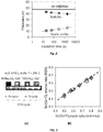
- the flow sequence and a schematic cross-section of the MIMcap stack are shown in Fig. 1 .
- Ruthenium films with a thickness of 5 nm were deposited by ALD with excellent smooth surfaces (lower than 0.2 nm RMS by AFM) on 10 nm TiN. Some wafers were left without Ru, i.e. with TiN bottom electrode (BE), for comparison.
- a controlled oxidation process as shown in Fig. 2 was applied to the wafers with Ru BE, resulting in ultrathin, controlled oxidation of the surface forming a 1 nm ruthenium oxide (hereafter called 'RuOx') layer with no penalty in roughness (i.e. maintaining a value lower than 0.2 nm RMS by AFM).
- This controlled oxidation is obtained by subjecting the Ru bottom electrode layer to a low-pressure atmosphere consisting of O 2 or consisting of a mixture of O 2 and one or more inert gases such as N 2 .
- the pressure or partial pressure of O 2 is between 1mTorr and 10 Torr (i.e. between 0.13Pa and 1333.22Pa).
- the temperature during oxidation is between 200°C and 450°C.
- the oxidation time is between lmin and 30min, with lower oxidation times being applicable for higher temperatures.
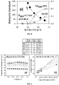
- STO films with a thickness of 7 to 9 nm were then deposited by ALD at 250°C using Sr(t-Bu 3 Cp) 2 and Ti(OCH 3 ) 4 precursors and H 2 O as oxidant.
- Good composition control over a large Sr/Ti range is obtained by adjusting the Sr to Ti pulse ratio as shown in Fig. 3 .
- Crystallized STO films were crystallized by rapid thermal processing (RTP) annealing in N 2 at a temperature lower or equal to 600°C.
- RTP rapid thermal processing
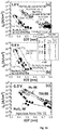
- the properties of crystallized STO films depend on the composition, as shown in Fig. 4 for films without TiO 2 interface layer, with k-value decreasing and lattice parameter increasing with increasing Sr. Only a small change is observed in band gap value.
- the resulting crystallized films Due to the intermixing, the resulting crystallized films have higher Ti content than the deposited STO films, and in consequence a higher k-value and lower EOT as shown in Figs. 9 and 6 . However, the films keep the favorable microstructure of the Sr-rich films.
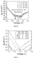
- Jg-EOT plots are shown in Fig. 12 , where data according to the invention are compared to best literature data for benchmarking. It is observed that the addition of TiO 2 layer results in a large decrease in EOT without much penalty in leakage. Low leakage values of Jg of 10 -6 A/cm 2 and 10 -8 A/cm 2 are achieved for EOT of 0.4 nm and 0.5 nm, respectively at 0.8V. These values are compared favorably with the state of the art MIMcaps with ALD grown high-k dielectrics, representing more than 100 x Jg reduction at 0.4 nm EOT.
- RuOx as bottom electrode instead of TiN or Ru provides a great advantage for leakage reduction. In this way leakage is reduced in both polarities for capacitors with TiN top electrodes.
- the improvement is due to the impact of the bottom electrode on STO dielectric quality, i.e. trap distribution, due to differences in oxygen scavenging during crystallization anneal.
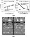
- Sr-rich STO films (7-10nm) were deposited on thin (0, 0.5, 1nm) TiO 2 layers on various bottom electrodes: TiN, Ru, RuO x .
- the RuO x bottom electrode was formed by low pressure oxidation of Ru at 250°C, resulting in a thin (1 Nm) RuO 2 layer on top of the Ru film.
- Both dielectrics were deposited by ALD, using Sr( t Bu 3 Cp) 2 and Ti(OMe) 4 as metal precursors and H 2 O as oxidizer, at 250°C.
- As deposited STO films are amorphous with k value ⁇ 20.
- the STO films were crystallized into the perovskite phase by rapid thermal processing (RTP) at 600°C in N 2 for 60s.
- RTP rapid thermal processing
- TiN top electrodes were then deposited and patterned, forming MIM capacitors.
- Fig. 13(a) shows the schematic cross section of a sample with RuO x bottom electrode and TiO 2 /Sr-rich STO dielectric stack, after dielectric deposition.
- Fig. 14(a) shows the EOT as function of deposited TiO 2 thickness for MIM capacitors with RuO x bottom electrodes and 9 nm (deposited) Sr-rich STO.
- a strong decrease in EOT is observed with increasing TiO 2 thickness.
- X-ray diffraction (XRD) patterns of the same dielectric stacks on RuOx, taken after crystallization anneal showed crystalline peaks corresponding to metastable perovskite STO, with no evidence of crystalline TiO 2 peaks.
- the 2-theta position of the STO (110) XRD peak is seen in Fig. 14(b) to increase with increasing TiO 2 layer thickness, indicating a corresponding decrease in lattice parameter.
- the final STO composition of a fully intermixed stack depends on the deposited thicknesses of both STO and TiO 2 layers, and varies in the range of Sr/(Sr+Ti) ⁇ 54-64% for the stacks explored in this set of experiments.
- the EOT of a fully intermixed layer can be calculated based on the known deposited Ti and Sr areal atomic concentrations as determined by Rutherford Backscattering Spectrometry (RBS), film thickness and densities as extracted from X-ray reflectivity analysis (XRR) and reported k-value dependence on STO Sr content. An excellent agreement is obtained between experimental EOT vs.
- Figure 15 (b) shows the comparison of the JG (EOT) trend lines at +0.8V obtained from the stacks of the disclosure (RuOx/1nmTiO 2 /STO/TiN - crosses, RuOx/0.5nm TiO 2 /STO/TiN - full symbols) with benchmark literature data (RuOx/Al doped Rutile TiO 2 /Pt - stars, and Ru/STO/Pt), showing more than 2 orders of magnitude Jg reduction at 0.45 nm EOT with RuOx/TiO 2 /STO stacks.
- the leakage at 0.45 nm EOT improves from 10 -5 A/cm 2 obtained for Al-doped Rutile TiO 2 to 10 -7 A/cm 2 with RuOx/0.5nm TiO 2 /STO/TiN and can be reduced further to ⁇ 3x10 -8 A/cm 2 when increasing the TiO 2 thickness from 0.5 to 1nm.
- ALD deposited TiO 2 /Sr-rich STO stacks intermix during crystallization anneal to form a perovskite STO dielectric with tailored (optimized) properties, including k-value tuned (by layer thicknesses) in the 50-100 range and small grain-size, crack-free microstructure, enabling to form capacitors with EOT in the 0.35-0.55 nm range with good electrical properties.
- tailored (optimized) properties including k-value tuned (by layer thicknesses) in the 50-100 range and small grain-size, crack-free microstructure, enabling to form capacitors with EOT in the 0.35-0.55 nm range with good electrical properties.
- the use of this stack approach in combination with oxidized Ru BE results in low leakage capacitors even at aggressively scaled EOTs, with significant leakage reduction compared to TiN or Ru BE.
- Leakage improvement for both polarities, larger for e-injection from oxidized Ru is attributed to reduction in trap density in STO in the vicinity of the oxidized Ru BE, in terms attributed to elimination or reversal of oxygen scavenging from the STO to the BE with RuOx BE.
Landscapes
- Engineering & Computer Science (AREA)
- Chemical & Material Sciences (AREA)
- Power Engineering (AREA)
- Microelectronics & Electronic Packaging (AREA)
- Computer Hardware Design (AREA)
- Manufacturing & Machinery (AREA)
- Materials Engineering (AREA)
- Physics & Mathematics (AREA)
- Condensed Matter Physics & Semiconductors (AREA)
- General Physics & Mathematics (AREA)
- Chemical Kinetics & Catalysis (AREA)
- Mechanical Engineering (AREA)
- Organic Chemistry (AREA)
- Metallurgy (AREA)
- General Chemical & Material Sciences (AREA)
- Inorganic Chemistry (AREA)
- Crystallography & Structural Chemistry (AREA)
- Semiconductor Memories (AREA)
- Chemical Vapour Deposition (AREA)
- Semiconductor Integrated Circuits (AREA)
Claims (8)
- Procédé de production d'un empilement de couches sur un substrat semiconducteur, le procédé comprenant les étapes de :• fourniture d'un substrat,• fourniture sur ledit substrat d'une première couche électriquement conductrice,• par dépôt de couche atomique, production d'un sous-empilement de couches sur ladite couche conductrice, au moins l'une desdites couches du sous-empilement étant une couche de TiO2, l'autre couche ou les autres couches du sous-empilement étant des couches d'un matériau diélectrique ayant une composition appropriée pour former une phase pérovskite cubique lors de la cristallisation dudit sous-empilement de couches,et comprenant en outre :• la soumission du substrat incluant ledit sous-empilement de couches à un traitement thermique pour ainsi cristalliser le sous-empilement de couches, de façon à obtenir une couche diélectrique cristallisée ayant une structure pérovskite cubique sur ladite première couche conductrice, par enchevêtrement complet de la couche ou des couches de TiO2 avec l'autre couche ou les autres couches du sous-empilement,• la production d'une seconde couche électriquement conductrice sur ladite couche diélectrique cristallisée.ou :• production d'une seconde couche électriquement conductrice sur ladite sous-empilement de couches,• soumission du substrat incluant ledit sous-empilement de couches et de ladite seconde couche conductrice à un traitement thermique pour ainsi cristalliser le sous-empilement de couches, de façon à obtenir une couche diélectrique cristallisée ayant une structure pérovskite cubique sur ladite première couche conductrice, par enchevêtrement complet de la couche ou des couches de TiO2 avec l'autre couche ou les autres couches du sous-empilement.dans lequel :- la couche ou les couches d'un matériau diélectrique ayant une composition appropriée pour former une phase pérovskite cubique lors de la cristallisation dudit sous-empilement de couches sont :∘ une ou plusieurs couches d'oxyde de strontium et de titane STO riche en strontium dans une phase métastable dans lequel le rapport Sr/(Sr+Ti) est supérieur à 50 %, et éventuellement une ou plusieurs couches d'oxyde de strontium SrO
ou∘ une ou plusieurs couches d'oxyde de strontium et de titane STO riche en titane dans une phase métastable dans lequel le rapport de Sr/(Sr+Ti) est inférieur à 50 % et une ou plusieurs couches d'oxyde de strontium (SrO),- la couche diélectrique cristallisée ayant une structure pérovskite cubique est une couche d'oxyde de strontium et de titane STO riche en strontium dans lequel le rapport Sr/(Sr+Ti) est supérieur à 50 %. - Procédé selon la revendication 1, dans lequel ledit sous-empilement de couches est produit par les étapes suivantes :• par dépôt de couche atomique, dépôt sur ladite première couche conductrice de ladite couche de TiO2,• par dépôt de couche atomique, dépôt sur ladite couche de TiO2 intermédiaire, de ladite couche d'un matériau diélectrique ayant une composition appropriée pour former une phase pérovskite cubique lors de la cristallisation.
- Procédé selon la revendication 1, dans lequel ledit sous-empilement de couches est produit par les étapes suivantes :• par dépôt de couche atomique, dépôt sur ladite première couche conductrice, de ladite couche d'un matériau diélectrique ayant une composition appropriée pour former une phase pérovskite cubique lors de la cristallisation,• par dépôt de couche atomique, dépôt sur ladite couche de matériau diélectrique, de ladite couche de TiO2.
- Procédé selon l'une quelconque des revendications précédentes, dans lequel une séquence de couches de TiO2 et de couches d'un matériau diélectrique alternées ou vice versa est déposée par dépôt de couche atomique sur ladite première couche conductrice de façon à former ledit sous-empilement de couches.
- Procédé selon l'une quelconque des revendications précédentes, dans lequel le rapport Sr/(Sr+Ti) de ladite couche STO métastable est entre 51 % et 65 %.
- Procédé selon l'une quelconque des revendications précédentes, dans lequel ledit traitement thermique est un recuit thermique à une température inférieure ou égale à 600 °C dans une atmosphère inerte.
- Procédé selon l'une quelconque des revendications précédentes, dans lequel ladite première couche conductrice comprend au moins au niveau de sa surface supérieure un matériau qui stocke un excès d'oxygène, créant un réservoir d'oxygène, et entraînant la libération d'oxygène depuis la première couche conductrice vers la diélectrique durant ledit traitement thermique, dans lequel ledit matériau qui stocke un excès d'oxygène est un oxyde de ruthénium.
- Procédé selon l'une quelconque des revendications précédentes dans lequel ladite seconde couche conductrice comprend au moins au niveau de sa surface inférieure un matériau qui stocke un excès d'oxygène, créant un réservoir d'oxygène, et entraînant la libération d'oxygène depuis la seconde couche conductrice vers la diélectrique durant un traitement thermique ultérieur, dans lequel ledit matériau qui stocke un excès d'oxygène est un oxyde de ruthénium.
Priority Applications (1)
| Application Number | Priority Date | Filing Date | Title |
|---|---|---|---|
| EP11182813.3A EP2434531B1 (fr) | 2010-09-28 | 2011-09-26 | Procédé de fabrication pour un condensateur métal-isolant-métal |
Applications Claiming Priority (3)
| Application Number | Priority Date | Filing Date | Title |
|---|---|---|---|
| EP10181359 | 2010-09-28 | ||
| US201161481393P | 2011-05-02 | 2011-05-02 | |
| EP11182813.3A EP2434531B1 (fr) | 2010-09-28 | 2011-09-26 | Procédé de fabrication pour un condensateur métal-isolant-métal |
Publications (3)
| Publication Number | Publication Date |
|---|---|
| EP2434531A2 EP2434531A2 (fr) | 2012-03-28 |
| EP2434531A3 EP2434531A3 (fr) | 2015-06-10 |
| EP2434531B1 true EP2434531B1 (fr) | 2019-12-04 |
Family
ID=44677739
Family Applications (1)
| Application Number | Title | Priority Date | Filing Date |
|---|---|---|---|
| EP11182813.3A Active EP2434531B1 (fr) | 2010-09-28 | 2011-09-26 | Procédé de fabrication pour un condensateur métal-isolant-métal |
Country Status (3)
| Country | Link |
|---|---|
| US (1) | US9343298B2 (fr) |
| EP (1) | EP2434531B1 (fr) |
| JP (1) | JP5888916B2 (fr) |
Families Citing this family (9)
| Publication number | Priority date | Publication date | Assignee | Title |
|---|---|---|---|---|
| US8835273B2 (en) * | 2012-09-19 | 2014-09-16 | Intermolecular, Inc. | High temperature ALD process of metal oxide for DRAM applications |
| US9231046B2 (en) | 2013-03-15 | 2016-01-05 | Globalfoundries Inc. | Capacitor using barrier layer metallurgy |
| US9647094B2 (en) | 2013-08-02 | 2017-05-09 | University Of Kentucky Research Foundation | Method of manufacturing a semiconductor heteroepitaxy structure |
| JP6583014B2 (ja) | 2016-01-22 | 2019-10-02 | 株式会社デンソー | 半導体装置の製造方法 |
| EP3660933A1 (fr) | 2018-11-30 | 2020-06-03 | IMEC vzw | Structure pour une utilisation dans un condensateur métal-isolant-métal |
| CN110415974B (zh) * | 2019-07-17 | 2021-04-02 | 南京大学 | 一种基于纳米叠层结构金属氧化物柔性电容器及其制备方法 |
| US11038013B2 (en) * | 2019-07-24 | 2021-06-15 | International Business Machines Corporation | Back-end-of-line compatible metal-insulator-metal on-chip decoupling capacitor |
| EP3840073A1 (fr) * | 2019-12-18 | 2021-06-23 | Imec VZW | Procédé de fabrication d'une structure magnétique pour un dispositif magnétique présentant un effet vcma géant |
| US20230008075A1 (en) * | 2021-07-08 | 2023-01-12 | Taiwan Semiconductor Manufacturing Company Ltd. | Capacitor structure and manufacturing method and operating method thereof |
Family Cites Families (11)
| Publication number | Priority date | Publication date | Assignee | Title |
|---|---|---|---|---|
| FI108375B (fi) | 1998-09-11 | 2002-01-15 | Asm Microchemistry Oy | Menetelmõ eristõvien oksidiohutkalvojen valmistamiseksi |
| US6388285B1 (en) * | 1999-06-04 | 2002-05-14 | International Business Machines Corporation | Feram cell with internal oxygen source and method of oxygen release |
| US6475854B2 (en) * | 1999-12-30 | 2002-11-05 | Applied Materials, Inc. | Method of forming metal electrodes |
| KR20030025672A (ko) * | 2001-09-22 | 2003-03-29 | 주식회사 하이닉스반도체 | 반도체 소자의 커패시터 제조방법 |
| US20060151822A1 (en) * | 2005-01-07 | 2006-07-13 | Shrinivas Govindarajan | DRAM with high K dielectric storage capacitor and method of making the same |
| US7892964B2 (en) * | 2007-02-14 | 2011-02-22 | Micron Technology, Inc. | Vapor deposition methods for forming a metal-containing layer on a substrate |
| US8945675B2 (en) | 2008-05-29 | 2015-02-03 | Asm International N.V. | Methods for forming conductive titanium oxide thin films |
| JP2010056392A (ja) * | 2008-08-29 | 2010-03-11 | Elpida Memory Inc | キャパシタ用絶縁膜、キャパシタ素子、キャパシタ用絶縁膜の製造方法及び半導体装置 |
| EP2166562B1 (fr) * | 2008-09-22 | 2019-03-20 | IMEC vzw | Procédé de formation par ALD d'un condensateur doté d'une couche diélectrique à base de dioxyde de titane de strontium |
| US7939442B2 (en) * | 2009-04-10 | 2011-05-10 | Micron Technology, Inc. | Strontium ruthenium oxide interface |
| US8202808B2 (en) | 2009-06-03 | 2012-06-19 | Intermolecular, Inc. | Methods of forming strontium titanate films |
-
2011
- 2011-09-26 US US13/245,247 patent/US9343298B2/en active Active
- 2011-09-26 EP EP11182813.3A patent/EP2434531B1/fr active Active
- 2011-09-27 JP JP2011210351A patent/JP5888916B2/ja not_active Expired - Fee Related
Non-Patent Citations (1)
| Title |
|---|
| None * |
Also Published As
| Publication number | Publication date |
|---|---|
| JP5888916B2 (ja) | 2016-03-22 |
| JP2012074702A (ja) | 2012-04-12 |
| EP2434531A2 (fr) | 2012-03-28 |
| US9343298B2 (en) | 2016-05-17 |
| US20120092807A1 (en) | 2012-04-19 |
| EP2434531A3 (fr) | 2015-06-10 |
Similar Documents
| Publication | Publication Date | Title |
|---|---|---|
| EP2434531B1 (fr) | Procédé de fabrication pour un condensateur métal-isolant-métal | |
| KR101123433B1 (ko) | 고 유전률을 갖는 구조물을 형성하는 방법 및 고 유전률을 갖는 구조물 | |
| JP5517918B2 (ja) | キャパシタとそれを有する半導体装置並びにそれらの製造方法 | |
| EP2166562B1 (fr) | Procédé de formation par ALD d'un condensateur doté d'une couche diélectrique à base de dioxyde de titane de strontium | |
| US9887083B2 (en) | Methods of forming capacitors | |
| US8092862B2 (en) | Method for forming dielectric film and method for forming capacitor in semiconductor device using the same | |
| US20130100577A1 (en) | Method for Forming a MIMCAP Structure and the MIMCAP Structure Thereof | |
| US20060289921A1 (en) | Method of manufacturing a capacitor for semiconductor device | |
| US8649154B2 (en) | Method for producing a metal-insulator-metal capacitor for use in semiconductor devices | |
| WO2020102416A1 (fr) | Films minces nanocristallins à faible fuite à k élevé | |
| JP2009027017A (ja) | 絶縁体膜、キャパシタ素子、dram及び半導体装置 | |
| JP5262233B2 (ja) | 窒化ジルコニウム界面層を有するキャパシター構造 | |
| US8530348B1 (en) | Integration of non-noble DRAM electrode | |
| Ko et al. | Improved dielectric constant and leakage current characteristics of BaTiO3 thin film on SrRuO3 seed layer | |
| Menou et al. | Seed Layer and Multistack Approaches to Reduce Leakage in SrTiO3-Based Metal–Insulator–Metal Capacitors Using TiN Bottom Electrode | |
| Pawlak et al. | Enabling 3X nm DRAM: Record low leakage 0.4 nm EOT MIM capacitors with novel stack engineering | |
| Kim et al. | Advanced Capacitor Dielectrics: Towards 2x nm DRAM | |
| US7198959B2 (en) | Process for fabrication of a ferrocapacitor | |
| Popovici et al. | Advanced dielectrics targeting 2X DRAM MIM capacitors | |
| Teng et al. | Effect of TiN treated by rapid thermal annealing on properties of BST capacitors prepared by RF magnetron co-sputter system at low substrate temperature |
Legal Events
| Date | Code | Title | Description |
|---|---|---|---|
| PUAI | Public reference made under article 153(3) epc to a published international application that has entered the european phase |
Free format text: ORIGINAL CODE: 0009012 |
|
| AK | Designated contracting states |
Kind code of ref document: A2 Designated state(s): AL AT BE BG CH CY CZ DE DK EE ES FI FR GB GR HR HU IE IS IT LI LT LU LV MC MK MT NL NO PL PT RO RS SE SI SK SM TR |
|
| AX | Request for extension of the european patent |
Extension state: BA ME |
|
| RIC1 | Information provided on ipc code assigned before grant |
Ipc: H01L 21/02 20060101AFI20150202BHEP Ipc: H01L 49/02 20060101ALI20150202BHEP Ipc: C23C 16/40 20060101ALI20150202BHEP Ipc: C23C 16/455 20060101ALI20150202BHEP |
|
| PUAL | Search report despatched |
Free format text: ORIGINAL CODE: 0009013 |
|
| AK | Designated contracting states |
Kind code of ref document: A3 Designated state(s): AL AT BE BG CH CY CZ DE DK EE ES FI FR GB GR HR HU IE IS IT LI LT LU LV MC MK MT NL NO PL PT RO RS SE SI SK SM TR |
|
| AX | Request for extension of the european patent |
Extension state: BA ME |
|
| RIC1 | Information provided on ipc code assigned before grant |
Ipc: C23C 16/455 20060101ALI20150506BHEP Ipc: H01L 49/02 20060101ALI20150506BHEP Ipc: C23C 16/40 20060101ALI20150506BHEP Ipc: H01L 21/02 20060101AFI20150506BHEP |
|
| 17P | Request for examination filed |
Effective date: 20151208 |
|
| RBV | Designated contracting states (corrected) |
Designated state(s): AL AT BE BG CH CY CZ DE DK EE ES FI FR GB GR HR HU IE IS IT LI LT LU LV MC MK MT NL NO PL PT RO RS SE SI SK SM TR |
|
| 17Q | First examination report despatched |
Effective date: 20160503 |
|
| RAP1 | Party data changed (applicant data changed or rights of an application transferred) |
Owner name: IMEC VZW |
|
| STAA | Information on the status of an ep patent application or granted ep patent |
Free format text: STATUS: EXAMINATION IS IN PROGRESS |
|
| GRAP | Despatch of communication of intention to grant a patent |
Free format text: ORIGINAL CODE: EPIDOSNIGR1 |
|
| STAA | Information on the status of an ep patent application or granted ep patent |
Free format text: STATUS: GRANT OF PATENT IS INTENDED |
|
| INTG | Intention to grant announced |
Effective date: 20190919 |
|
| GRAS | Grant fee paid |
Free format text: ORIGINAL CODE: EPIDOSNIGR3 |
|
| GRAA | (expected) grant |
Free format text: ORIGINAL CODE: 0009210 |
|
| STAA | Information on the status of an ep patent application or granted ep patent |
Free format text: STATUS: THE PATENT HAS BEEN GRANTED |
|
| AK | Designated contracting states |
Kind code of ref document: B1 Designated state(s): AL AT BE BG CH CY CZ DE DK EE ES FI FR GB GR HR HU IE IS IT LI LT LU LV MC MK MT NL NO PL PT RO RS SE SI SK SM TR |
|
| REG | Reference to a national code |
Ref country code: GB Ref legal event code: FG4D |
|
| REG | Reference to a national code |
Ref country code: CH Ref legal event code: EP |
|
| REG | Reference to a national code |
Ref country code: AT Ref legal event code: REF Ref document number: 1210453 Country of ref document: AT Kind code of ref document: T Effective date: 20191215 |
|
| REG | Reference to a national code |
Ref country code: DE Ref legal event code: R096 Ref document number: 602011063762 Country of ref document: DE |
|
| REG | Reference to a national code |
Ref country code: IE Ref legal event code: FG4D |
|
| REG | Reference to a national code |
Ref country code: NL Ref legal event code: MP Effective date: 20191204 |
|
| REG | Reference to a national code |
Ref country code: LT Ref legal event code: MG4D |
|
| PG25 | Lapsed in a contracting state [announced via postgrant information from national office to epo] |
Ref country code: SE Free format text: LAPSE BECAUSE OF FAILURE TO SUBMIT A TRANSLATION OF THE DESCRIPTION OR TO PAY THE FEE WITHIN THE PRESCRIBED TIME-LIMIT Effective date: 20191204 Ref country code: BG Free format text: LAPSE BECAUSE OF FAILURE TO SUBMIT A TRANSLATION OF THE DESCRIPTION OR TO PAY THE FEE WITHIN THE PRESCRIBED TIME-LIMIT Effective date: 20200304 Ref country code: LT Free format text: LAPSE BECAUSE OF FAILURE TO SUBMIT A TRANSLATION OF THE DESCRIPTION OR TO PAY THE FEE WITHIN THE PRESCRIBED TIME-LIMIT Effective date: 20191204 Ref country code: FI Free format text: LAPSE BECAUSE OF FAILURE TO SUBMIT A TRANSLATION OF THE DESCRIPTION OR TO PAY THE FEE WITHIN THE PRESCRIBED TIME-LIMIT Effective date: 20191204 Ref country code: ES Free format text: LAPSE BECAUSE OF FAILURE TO SUBMIT A TRANSLATION OF THE DESCRIPTION OR TO PAY THE FEE WITHIN THE PRESCRIBED TIME-LIMIT Effective date: 20191204 Ref country code: LV Free format text: LAPSE BECAUSE OF FAILURE TO SUBMIT A TRANSLATION OF THE DESCRIPTION OR TO PAY THE FEE WITHIN THE PRESCRIBED TIME-LIMIT Effective date: 20191204 Ref country code: GR Free format text: LAPSE BECAUSE OF FAILURE TO SUBMIT A TRANSLATION OF THE DESCRIPTION OR TO PAY THE FEE WITHIN THE PRESCRIBED TIME-LIMIT Effective date: 20200305 Ref country code: NO Free format text: LAPSE BECAUSE OF FAILURE TO SUBMIT A TRANSLATION OF THE DESCRIPTION OR TO PAY THE FEE WITHIN THE PRESCRIBED TIME-LIMIT Effective date: 20200304 |
|
| PG25 | Lapsed in a contracting state [announced via postgrant information from national office to epo] |
Ref country code: RS Free format text: LAPSE BECAUSE OF FAILURE TO SUBMIT A TRANSLATION OF THE DESCRIPTION OR TO PAY THE FEE WITHIN THE PRESCRIBED TIME-LIMIT Effective date: 20191204 Ref country code: HR Free format text: LAPSE BECAUSE OF FAILURE TO SUBMIT A TRANSLATION OF THE DESCRIPTION OR TO PAY THE FEE WITHIN THE PRESCRIBED TIME-LIMIT Effective date: 20191204 |
|
| PG25 | Lapsed in a contracting state [announced via postgrant information from national office to epo] |
Ref country code: AL Free format text: LAPSE BECAUSE OF FAILURE TO SUBMIT A TRANSLATION OF THE DESCRIPTION OR TO PAY THE FEE WITHIN THE PRESCRIBED TIME-LIMIT Effective date: 20191204 |
|
| PG25 | Lapsed in a contracting state [announced via postgrant information from national office to epo] |
Ref country code: CZ Free format text: LAPSE BECAUSE OF FAILURE TO SUBMIT A TRANSLATION OF THE DESCRIPTION OR TO PAY THE FEE WITHIN THE PRESCRIBED TIME-LIMIT Effective date: 20191204 Ref country code: RO Free format text: LAPSE BECAUSE OF FAILURE TO SUBMIT A TRANSLATION OF THE DESCRIPTION OR TO PAY THE FEE WITHIN THE PRESCRIBED TIME-LIMIT Effective date: 20191204 Ref country code: PT Free format text: LAPSE BECAUSE OF FAILURE TO SUBMIT A TRANSLATION OF THE DESCRIPTION OR TO PAY THE FEE WITHIN THE PRESCRIBED TIME-LIMIT Effective date: 20200429 Ref country code: EE Free format text: LAPSE BECAUSE OF FAILURE TO SUBMIT A TRANSLATION OF THE DESCRIPTION OR TO PAY THE FEE WITHIN THE PRESCRIBED TIME-LIMIT Effective date: 20191204 Ref country code: NL Free format text: LAPSE BECAUSE OF FAILURE TO SUBMIT A TRANSLATION OF THE DESCRIPTION OR TO PAY THE FEE WITHIN THE PRESCRIBED TIME-LIMIT Effective date: 20191204 |
|
| PG25 | Lapsed in a contracting state [announced via postgrant information from national office to epo] |
Ref country code: SK Free format text: LAPSE BECAUSE OF FAILURE TO SUBMIT A TRANSLATION OF THE DESCRIPTION OR TO PAY THE FEE WITHIN THE PRESCRIBED TIME-LIMIT Effective date: 20191204 Ref country code: SM Free format text: LAPSE BECAUSE OF FAILURE TO SUBMIT A TRANSLATION OF THE DESCRIPTION OR TO PAY THE FEE WITHIN THE PRESCRIBED TIME-LIMIT Effective date: 20191204 Ref country code: IS Free format text: LAPSE BECAUSE OF FAILURE TO SUBMIT A TRANSLATION OF THE DESCRIPTION OR TO PAY THE FEE WITHIN THE PRESCRIBED TIME-LIMIT Effective date: 20200404 |
|
| REG | Reference to a national code |
Ref country code: DE Ref legal event code: R097 Ref document number: 602011063762 Country of ref document: DE |
|
| REG | Reference to a national code |
Ref country code: AT Ref legal event code: MK05 Ref document number: 1210453 Country of ref document: AT Kind code of ref document: T Effective date: 20191204 |
|
| PLBE | No opposition filed within time limit |
Free format text: ORIGINAL CODE: 0009261 |
|
| STAA | Information on the status of an ep patent application or granted ep patent |
Free format text: STATUS: NO OPPOSITION FILED WITHIN TIME LIMIT |
|
| PG25 | Lapsed in a contracting state [announced via postgrant information from national office to epo] |
Ref country code: DK Free format text: LAPSE BECAUSE OF FAILURE TO SUBMIT A TRANSLATION OF THE DESCRIPTION OR TO PAY THE FEE WITHIN THE PRESCRIBED TIME-LIMIT Effective date: 20191204 |
|
| 26N | No opposition filed |
Effective date: 20200907 |
|
| PG25 | Lapsed in a contracting state [announced via postgrant information from national office to epo] |
Ref country code: AT Free format text: LAPSE BECAUSE OF FAILURE TO SUBMIT A TRANSLATION OF THE DESCRIPTION OR TO PAY THE FEE WITHIN THE PRESCRIBED TIME-LIMIT Effective date: 20191204 Ref country code: PL Free format text: LAPSE BECAUSE OF FAILURE TO SUBMIT A TRANSLATION OF THE DESCRIPTION OR TO PAY THE FEE WITHIN THE PRESCRIBED TIME-LIMIT Effective date: 20191204 Ref country code: SI Free format text: LAPSE BECAUSE OF FAILURE TO SUBMIT A TRANSLATION OF THE DESCRIPTION OR TO PAY THE FEE WITHIN THE PRESCRIBED TIME-LIMIT Effective date: 20191204 |
|
| PG25 | Lapsed in a contracting state [announced via postgrant information from national office to epo] |
Ref country code: IT Free format text: LAPSE BECAUSE OF FAILURE TO SUBMIT A TRANSLATION OF THE DESCRIPTION OR TO PAY THE FEE WITHIN THE PRESCRIBED TIME-LIMIT Effective date: 20191204 |
|
| REG | Reference to a national code |
Ref country code: DE Ref legal event code: R119 Ref document number: 602011063762 Country of ref document: DE |
|
| PG25 | Lapsed in a contracting state [announced via postgrant information from national office to epo] |
Ref country code: MC Free format text: LAPSE BECAUSE OF FAILURE TO SUBMIT A TRANSLATION OF THE DESCRIPTION OR TO PAY THE FEE WITHIN THE PRESCRIBED TIME-LIMIT Effective date: 20191204 |
|
| REG | Reference to a national code |
Ref country code: CH Ref legal event code: PL |
|
| GBPC | Gb: european patent ceased through non-payment of renewal fee |
Effective date: 20200926 |
|
| REG | Reference to a national code |
Ref country code: BE Ref legal event code: MM Effective date: 20200930 |
|
| PG25 | Lapsed in a contracting state [announced via postgrant information from national office to epo] |
Ref country code: LU Free format text: LAPSE BECAUSE OF NON-PAYMENT OF DUE FEES Effective date: 20200926 |
|
| PG25 | Lapsed in a contracting state [announced via postgrant information from national office to epo] |
Ref country code: FR Free format text: LAPSE BECAUSE OF NON-PAYMENT OF DUE FEES Effective date: 20200930 Ref country code: DE Free format text: LAPSE BECAUSE OF NON-PAYMENT OF DUE FEES Effective date: 20210401 |
|
| PG25 | Lapsed in a contracting state [announced via postgrant information from national office to epo] |
Ref country code: BE Free format text: LAPSE BECAUSE OF NON-PAYMENT OF DUE FEES Effective date: 20200930 Ref country code: CH Free format text: LAPSE BECAUSE OF NON-PAYMENT OF DUE FEES Effective date: 20200930 Ref country code: GB Free format text: LAPSE BECAUSE OF NON-PAYMENT OF DUE FEES Effective date: 20200926 Ref country code: IE Free format text: LAPSE BECAUSE OF NON-PAYMENT OF DUE FEES Effective date: 20200926 Ref country code: LI Free format text: LAPSE BECAUSE OF NON-PAYMENT OF DUE FEES Effective date: 20200930 |
|
| PG25 | Lapsed in a contracting state [announced via postgrant information from national office to epo] |
Ref country code: TR Free format text: LAPSE BECAUSE OF FAILURE TO SUBMIT A TRANSLATION OF THE DESCRIPTION OR TO PAY THE FEE WITHIN THE PRESCRIBED TIME-LIMIT Effective date: 20191204 Ref country code: MT Free format text: LAPSE BECAUSE OF FAILURE TO SUBMIT A TRANSLATION OF THE DESCRIPTION OR TO PAY THE FEE WITHIN THE PRESCRIBED TIME-LIMIT Effective date: 20191204 Ref country code: CY Free format text: LAPSE BECAUSE OF FAILURE TO SUBMIT A TRANSLATION OF THE DESCRIPTION OR TO PAY THE FEE WITHIN THE PRESCRIBED TIME-LIMIT Effective date: 20191204 |
|
| PG25 | Lapsed in a contracting state [announced via postgrant information from national office to epo] |
Ref country code: MK Free format text: LAPSE BECAUSE OF FAILURE TO SUBMIT A TRANSLATION OF THE DESCRIPTION OR TO PAY THE FEE WITHIN THE PRESCRIBED TIME-LIMIT Effective date: 20191204 |