EP2428318A2 - Verfahren zum Polieren eines Objekts zum Bilden einer konvexen oder konkaven Oberfläche auf diesem Objekt und Polierkissen - Google Patents
Verfahren zum Polieren eines Objekts zum Bilden einer konvexen oder konkaven Oberfläche auf diesem Objekt und Polierkissen Download PDFInfo
- Publication number
- EP2428318A2 EP2428318A2 EP11180163A EP11180163A EP2428318A2 EP 2428318 A2 EP2428318 A2 EP 2428318A2 EP 11180163 A EP11180163 A EP 11180163A EP 11180163 A EP11180163 A EP 11180163A EP 2428318 A2 EP2428318 A2 EP 2428318A2
- Authority
- EP
- European Patent Office
- Prior art keywords
- polishing
- polished
- region
- polishing pad
- grooves
- Prior art date
- Legal status (The legal status is an assumption and is not a legal conclusion. Google has not performed a legal analysis and makes no representation as to the accuracy of the status listed.)
- Withdrawn
Links
Images



Classifications
-
- B—PERFORMING OPERATIONS; TRANSPORTING
- B24—GRINDING; POLISHING
- B24B—MACHINES, DEVICES, OR PROCESSES FOR GRINDING OR POLISHING; DRESSING OR CONDITIONING OF ABRADING SURFACES; FEEDING OF GRINDING, POLISHING, OR LAPPING AGENTS
- B24B37/00—Lapping machines or devices; Accessories
- B24B37/04—Lapping machines or devices; Accessories designed for working plane surfaces
- B24B37/042—Lapping machines or devices; Accessories designed for working plane surfaces operating processes therefor
-
- H—ELECTRICITY
- H10—SEMICONDUCTOR DEVICES; ELECTRIC SOLID-STATE DEVICES NOT OTHERWISE PROVIDED FOR
- H10P—GENERIC PROCESSES OR APPARATUS FOR THE MANUFACTURE OR TREATMENT OF DEVICES COVERED BY CLASS H10
- H10P52/00—Grinding, lapping or polishing of wafers, substrates or parts of devices
-
- B—PERFORMING OPERATIONS; TRANSPORTING
- B24—GRINDING; POLISHING
- B24B—MACHINES, DEVICES, OR PROCESSES FOR GRINDING OR POLISHING; DRESSING OR CONDITIONING OF ABRADING SURFACES; FEEDING OF GRINDING, POLISHING, OR LAPPING AGENTS
- B24B13/00—Machines or devices designed for grinding or polishing optical surfaces on lenses or surfaces of similar shape on other work; Accessories therefor
-
- B—PERFORMING OPERATIONS; TRANSPORTING
- B24—GRINDING; POLISHING
- B24B—MACHINES, DEVICES, OR PROCESSES FOR GRINDING OR POLISHING; DRESSING OR CONDITIONING OF ABRADING SURFACES; FEEDING OF GRINDING, POLISHING, OR LAPPING AGENTS
- B24B37/00—Lapping machines or devices; Accessories
-
- B—PERFORMING OPERATIONS; TRANSPORTING
- B24—GRINDING; POLISHING
- B24B—MACHINES, DEVICES, OR PROCESSES FOR GRINDING OR POLISHING; DRESSING OR CONDITIONING OF ABRADING SURFACES; FEEDING OF GRINDING, POLISHING, OR LAPPING AGENTS
- B24B37/00—Lapping machines or devices; Accessories
- B24B37/005—Control means for lapping machines or devices
- B24B37/0056—Control means for lapping machines or devices taking regard of the pH-value of lapping agents
-
- B—PERFORMING OPERATIONS; TRANSPORTING
- B24—GRINDING; POLISHING
- B24B—MACHINES, DEVICES, OR PROCESSES FOR GRINDING OR POLISHING; DRESSING OR CONDITIONING OF ABRADING SURFACES; FEEDING OF GRINDING, POLISHING, OR LAPPING AGENTS
- B24B37/00—Lapping machines or devices; Accessories
- B24B37/11—Lapping tools
- B24B37/20—Lapping pads for working plane surfaces
- B24B37/26—Lapping pads for working plane surfaces characterised by the shape of the lapping pad surface, e.g. grooved
-
- B—PERFORMING OPERATIONS; TRANSPORTING
- B24—GRINDING; POLISHING
- B24B—MACHINES, DEVICES, OR PROCESSES FOR GRINDING OR POLISHING; DRESSING OR CONDITIONING OF ABRADING SURFACES; FEEDING OF GRINDING, POLISHING, OR LAPPING AGENTS
- B24B57/00—Devices for feeding, applying, grading or recovering grinding, polishing or lapping agents
- B24B57/02—Devices for feeding, applying, grading or recovering grinding, polishing or lapping agents for feeding of fluid, sprayed, pulverised, or liquefied grinding, polishing or lapping agents
-
- B—PERFORMING OPERATIONS; TRANSPORTING
- B24—GRINDING; POLISHING
- B24B—MACHINES, DEVICES, OR PROCESSES FOR GRINDING OR POLISHING; DRESSING OR CONDITIONING OF ABRADING SURFACES; FEEDING OF GRINDING, POLISHING, OR LAPPING AGENTS
- B24B7/00—Machines or devices designed for grinding plane surfaces on work, including polishing plane glass surfaces; Accessories therefor
- B24B7/20—Machines or devices designed for grinding plane surfaces on work, including polishing plane glass surfaces; Accessories therefor characterised by a special design with respect to properties of the material of non-metallic articles to be ground
- B24B7/22—Machines or devices designed for grinding plane surfaces on work, including polishing plane glass surfaces; Accessories therefor characterised by a special design with respect to properties of the material of non-metallic articles to be ground for grinding inorganic material, e.g. stone, ceramics, porcelain
- B24B7/228—Machines or devices designed for grinding plane surfaces on work, including polishing plane glass surfaces; Accessories therefor characterised by a special design with respect to properties of the material of non-metallic articles to be ground for grinding inorganic material, e.g. stone, ceramics, porcelain for grinding thin, brittle parts, e.g. semiconductors, wafers
Definitions
- the present invention relates to: a method of polishing an object to be polished for processing the surface of the obj ect to be polished into a convex or concave state; and a polishing pad.
- CMP Chemical mechanical polishing
- An object of the present invention is to provide: a polishing method of an object to be polished for processing a surface of the object to be polished into a concave or convex state with a high degree of accuracy by polishing the surface; and a polishing pad.
- a method of polishing an object to be polished according to the present invention makes it possible to process the surface of the object to be polished such as a semiconductor wafer into a concave or convex state.
- the present invention provides a method of polishing an object to be polished and a polishing pad, stated below.
- a method of polishing an object to be polished according to the present invention makes it possible to process the surface of the object to be polished into a concave or convex state. Since polishing conditions can be determined by the type of a polishing pad, number of revolutions, and slurry, the optimization of the conditions is facilitated.
- a polishing method according to the present invention is a polishing method used in chemical mechanical polishing (CMP) for polishing the surface of an object to be polished such as a semiconductor wafer.
- CMP chemical mechanical polishing
- a schematic view of a CMP apparatus 1 is shown in Fig. 1 .
- the CMP apparatus 1 includes a platen 2, a polishing head 3, and a slurry supply unit 4.
- a polishing pad 10 is attached to the platen 2.
- the surface of an object to be polished 20 is polished chemically and mechanically by: supplying slurry onto the polishing pad 10 from the slurry supply unit 4; rotating the platen 2; and rotating the polishing head 3 in the same direction as the platen 2 while the polishing head 3 pushes the object to be polished 20 positioned on the polishing pad 10, with respect to the polishing pad 10.
- a polishing pad 10 has a first polishing region 11 where grooves 15 are formed and a second polishing region 12 where grooves 15 are formed in a different state from that of the first polishing region 11, wherein either one of the first polishing region 11 and the second polishing region 12 is formed on a region on the center side, and the other is formed on a region on the outer side in a radial direction on the surface of the polishing pad 10.
- the expression "different state from that of the first polishing region” includes a state where grooves 15 different from the ones of the first polishing region 11 are formed, or a state where no groove 15 is practically formed.
- the object to be polished 20 may be polished to a certain degree by this second polishing region 12 due to the friction between the surface of the second polishing region 12 and that of the object to be polished 20.
- the first polishing region 11 is a region where polishing is prone to proceed compared to the second polishing region 12. That is, the amount to be polished is larger in the first polishing region 11 compared to the second polishing region 12. As such, the first polishing region 11 may have more grooves in number per unit length in the radial direction compared to the second polishing region 12.
- the number, depth, width and the like of the grooves 15 of the first polishing region 11 may be freely chosen, depending upon the kind of the object to be polished 20, the aim of the polishing and the like.
- the width of the grooves 15 of the first polishing region 11 may be 0.2 mm to 0.8 mm, and the pitch of the grooves 15 (the distance between the centers of two grooves 15) may be about 1 mm to 2 mm.
- the pitch of the grooves 15 may be about 2.5 mm to 3.5 mm.
- the first polishing region 11 is formed on a region on the outer side and the second polishing region 12 on the inner side.
- the first polishing region 11 is formed on a region on the inner side and the second polishing region 12 on the outer side.
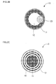
- FIG. 2A An embodiment of a polishing pad 10 is shown in Fig. 2A (an object to be polished 20 is placed in Fig. 2A ).
- the polishing pad 10 is formed into a disk shape, has a plurality of grooves 15 processed on the surface, is attached to a platen 2, and polishes an object to be polished 20.
- the polishing pad 10 is formed of, for example, foamed rigid urethane, suede or the like.
- Fig. 2A shows a polishing pad 10 having a first polishing region 11 formed on the center side in a radial direction and having concentric grooves 15 formed in the first polishing region 11.
- the region on the outer side in a radial direction is a second polishing region 12.
- Fig. 2A shows a case where the grooves 15 are not formed. It is possible to process the surface of an object to be polished 20 into a concave state (lower right side in Fig. 3 ) by using a polishing pad 10 having a first polishing region 11 formed on the center side as shown in Fig. 2A .
- Fig. 2B shows a polishing pad 10 having a first polishing region 11 formed on the outer side and having concentric grooves 15 formed in the first polishing region 11 (an object to be polished 20 is placed in Fig. 2B ).
- the region on the center side is a second polishing region 12.
- Fig. 2B shows a case where the grooves 15 are not formed. It is possible to process the surface of an object to be polished 20 into a convex state (lower left side in Fig. 3 ) by using a polishing pad 10 having a first polishing region 11 formed on the outer side as shown in Fig. 2B .
- FIG. 2C shows an embodiment where the second polishing region 12 is formed on the outer side of the polishing pad 10 with a small number of grooves 15.
- Fig. 2D shows an embodiment where the second polishing region 12 is formed on the center side of the polishing pad 10 with a small number of grooves 15.
- the second polishing region 12 has a smaller number of grooves 15 per unit length in the radial direction compared with the first polishing region 11.
- a method of polishing an object to be polished comprises the steps of: placing an object to be polished 20 on a polishing pad 10 over the boundary between the first polishing region 11 and the second polishing region 12, the polishing pad 10 having a first polishing region 11 where grooves 15 are formed and a second polishing region 12 where grooves 15 are formed in a different state from that of the first polishing region, and either one of the first polishing region 11 and the second polishing region 12 being formed on a region on the center side, and the other being formed on a region on the outer side in a radial direction on the surface of the polishing pad 10; and polishing the object to be polished 20 by rotating the polishing pad 10 and the object to be polished 20. Then, as shown in Fig.
- the surface of the object to be polished 20 is processed into a concave (lower right side in Fig. 3 ) or convex (lower left side in Fig. 3 ) state.
- a concave or convex crowning shape having a curvature radius of R 2 million mm to R 50 million mm.
- Examples of an object to be polished 20 in a method of polishing an object to be polished according to the present invention are: semiconductor wafers including Si, SiO 2 , etc.; monocrystal wafers including LN, LT, GaN, etc.; ceramics including alumina, zirconia, piezoelectric body, etc.; and metals including alloys of beryllium, copper, etc.
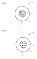
- FIG. 4A shows a polishing pad 10 having a first polishing region 11 formed on the center side and having lattice-shaped grooves 15 formed in the first polishing region 11.
- Fig. 4B shows a polishing pad 10 having a first polishing region 11 formed on the center side and having hole-shaped grooves 15 formed in the first polishing region 11.
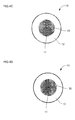
- Figs. 4C and 4D shows a polishing pad 10 having a first polishing region 11 formed on the center side and having spiral-shaped grooves 15 formed from the center of the polishing pad 10 in the first polishing region 11.
- each of Fig. 4A to 4D is the case of a polishing pad 10 having a first polishing region 11 formed on the center side, it is also possible to form a first polishing region 11 in the region on the outer side as shown in Fig. 2B .
- a polishing pad 10 having a first polishing region 11 formed on the outer side it is possible to process the surface of an object to be polished 20 into a convex state (lower left side in Fig. 3 ).
- the method of polishing an object to be polished according to Embodiment 2 of the present invention comprises the steps of placing an object to be polished 20 on a polishing pad 10 having grooves 15 formed on its surface; and polishing the object to be polished 20 by rotating the polishing pad 10 and the object to be polished 20 at number of revolutions different from each other so as to make polishing speed have a distribution on the surface of the object to be polished 20. By so doing, it is possible to process the surface of the object to be polished 20 into a concave or convex state.
- a polishing pad shown in Fig. 5 has a first polishing region 11 on the whole surface and lattice-shaped grooves 15 are formed in the first polishing region 11.
- a polishing pad 10 used in the method of polishing an object to be polished according to Embodiment 2 may be any polishing pad as long as grooves 15 are formed on the whole surface.
- the shape of the grooves in the first polishing region 11 is not limited.
- the revolution speed of a platen 2 is preferably 5 to 1,000 rpm, more preferably 10 to 500 rpm, and further preferably 10 to 150 rpm.
- the revolution speed of an object to be polished 20 is preferably 5 to 1,000 rpm, more preferably 10 to 500 rpm, and further preferably 10 to 150 rpm.
- the difference between the revolution speed of a platen 2 (a polishing pad 10) and the revolution speed of an object to be polished 20 is preferably 0 to 500 rpm (here 0 rpm is excluded), more preferably 0 to 450 rpm, and further preferably 0 to 100 rpm. If the increase in the curvature radius of the surface to be polished of an object to be polished 20 is required (for example, 50 million mm), it is preferable to bring the difference of the revolution speeds close to 0, but 0 rpm is not included.
- a method of polishing an object to be polished comprises the steps of: placing the object to be polished 20 on a polishing pad 10 having grooves 15 formed on its surface; and polishing the object to be polished 20 by rotating the polishing pad 10 and the object to be polished 20 while supplying one of two slurries having different properties each other to a region of the polishing pad 10 on the center side of the central part 20c of the object to be polished 20 in a radial direction of the polishing pad 10, and supplying the other slurry to a region of the polishing pad 10 on the outer side of the central part 20c of the object to be polished 20, respectively.
- the slurry may be supplied to only one of the said two regions, i.e. the region on the center side or the region on the outer side.
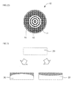
- a polishing pad 10 having concentric grooves 15 formed as shown in Fig. 6A is used.
- Fig. 6B is a schematic view showing the supply region of slurry. It is possible to form a concave surface on an object to be polished 20 by supplying slurry for polishing to the region of a polishing pad 10 on the center side of the central part 20c of the object to be polished 20 and supplying slurry for suppressing polishing to the region of the polishing pad 10 on the outer side of the central part 20c of the object to be polished 20.
- the slurry for polishing and the slurry for suppressing polishing have different pHs from each other.
- the polishing speed in the suppressing region is lower than the polishing speed in the polishing region by 30% to 100%.
- the slurry includes a polishing member, an acid, an oxidizer, and water.
- a polishing member colloidal silica, fumed silica, alumina, titania, zirconia, a mixture of these, etc. can be used.
- an oxidizer peroxide, nitrate, etc. can be used.
- the slurry may contain a pH adjuster.
- a pH adjuster an acidic substance or a basic substance is arbitrarily used in order to adjust the pH of the slurry to a desired value.
- the pH in the region of a polishing pad 10 on the center side of the central part 20c of an object to be polished 20 is preferably 0 to 12.0, more preferably 3.0 to 10.0, and further preferably 4.0 to 10.0.
- the pH in the region of a polishing pad 10 on the outer side of the central part 20c of an object to be polished 20 is preferably 10.0 to 14.0, more preferably 12.0 to 14.0, and further preferably 13.0 to 14.0. It should be noted that, if the pH value in the region on the center side and the pH value in the region on the outer side are reversed from the above values, concave and convex of a surface are also formed reversely.
- the polishing speed in acid (pH 3 to 5) is 200% (two times) and the polishing speed in strong alkali (pH 13 or higher) is approximately zero (0%) when the ordinary polishing speed through the use of colloidal silica is 1.
- an object to be polished 20 may also be polished while slurry is supplied only to either the region of a polishing pad 10 on the center side of the central part 20c of the object to be polished 20 or the region of a polishing pad 10 on the outer side of the central part 20c of the object to be polished 20 in a radial direction of the polishing pad 10.
- a polishing pad 10 ( Fig. 2A ) having a first polishing region 11 formed on the center side and having concentric grooves 15 formed in the first polishing region 11 was attached to a CMP apparatus 1 (refer to Fig. 1 ) and an object to be polished 20 was polished.
- a slurry a slurry containing colloidal silica as a polishing member was used.
- the width of the grooves 15 formed on the first polishing region 11 of the polishing pad 10 was 0.5 mm and the pitch was 1. 5 mm.
- a polishing pad 10 made of foamed rigid urethane was used.
- As the object to be polished 20, as shown in Fig. 7A a Si wafer 20b having a diameter of 100 mm where an SiO 2 film 20a having a thickness of 10,000 ⁇ is formed thereon was used.
- the object to be polished was placed at the boundary between the first polishing region 11 and the second polishing region 12 and polished as shown in Fig. 2A . Then the thickness of the SiO 2 film 20a of the wafer after having polished was measured at the positions shown in Fig. 8 through the use of a film thickness meter.
- Fig. 9 The results are shown in Fig. 9 .
- Fig. 9 it was possible to process the surface of an object to be polished 20 into a concave state as shown in Fig. 7B by using a polishing pad 10 having a first polishing region 11 formed on the center side.
- the curvature radius was R 36 million mm.
- An object to be polished 20 was polished by using a polishing pad 10 having lattice-shaped grooves 15 formed on the whole surface and having a diameter of 300 mm, and rotating the polishing pad 10 and the object to be polished 20 at different numbers of revolutions (refer to Fig. 5 ).
- the width of the grooves 15 formed on the first polishing region 11 of the polishing pad 10 was 0.5 mm and the pitch was 1.5 mm.
- a polishing pad 10 made of foamed rigid urethane was used.
- a Si wafer 20b having a diameter of 100 mm where an SiO 2 film 20a having a thickness of 10,000 ⁇ is formed thereon was used.
- the polishing pad 10 was rotated at 80 rpm and the object to be polished 20 was rotated at 40 rpm in the same direction.
- the results are shown in Fig. 10 .
- the 9 points in the range between -40 to 40 mm on the horizontal axis representing a measurement position in Fig. 10 correspond to the measurement positions 1 to 9 in Fig. 8 .
- the thickness of SiO 2 in the center region was reduced, showing that a concave surface was formed as shown in Fig. 7B .
- the curvature radius was R 13 million mm.
- An object to be polished 20 was polished by using the polishing pad 10 of Example 2 and rotating the polishing pad 10 and the object to be polished 20 at different numbers of revolutions (refer to Fig. 5 ).
- a Si wafer 20b having a diameter of 100 mm where an SiO 2 film 20a having a thickness of 10,000 ⁇ is formed thereon, which is the same as in Example 2 was used.
- the polishing pad 10 was rotated at 40 rpm and the object to be polished 20 was rotated at 80 rpm in the same direction.
- the results are shown in Fig. 11 .
- the thickness of SiO 2 in the center region was increased showing that a convex surface was formed as shown in Fig. 7C .
- the curvature radius was R 8.9 million mm.
- An object to be polished 20 was polished by using a polishing pad 10 having concentric grooves 15 formed on the whole surface and having a diameter of 300 mm (refer to Figs. 6A and 6B ).
- the width of the grooves 15 formed on the first polishing region 11 of the polishing pad 10 was 0.5 mm and the pitch was 1.5 mm.
- a polishing pad 10 made of foamed rigid urethane was used.
- a Si wafer 20b having a diameter of 100 mm where an SiO 2 film 20a having a thickness of 10,000 ⁇ is formed thereon was used.
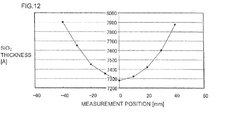
- the object to be polished 20 was polished while different slurries were supplied to the region of the polishing pad 10 on the center side of the central part 20c of the object to be polished 20 and to the region of the polishing pad 10 on the outer side of the central part 20c of the object to be polished 20, respectively, in a radial direction of the polishing pad 10.
- the slurries contained colloidal silica as abrasive grain, and pH of the slurry supplied to the region on the center side was 9 to 10 and pH of the slurry supplied to the region on the outer side was 13.
- the results are shown in Fig. 12 .
- the thickness of SiO 2 in the center region was reduced showing that a concave surface was formed as shown in Fig. 7B .
Landscapes
- Engineering & Computer Science (AREA)
- Mechanical Engineering (AREA)
- Chemical & Material Sciences (AREA)
- Ceramic Engineering (AREA)
- Inorganic Chemistry (AREA)
- Mechanical Treatment Of Semiconductor (AREA)
- Finish Polishing, Edge Sharpening, And Grinding By Specific Grinding Devices (AREA)
Priority Applications (1)
| Application Number | Priority Date | Filing Date | Title |
|---|---|---|---|
| EP19193021.3A EP3597365A1 (de) | 2010-09-09 | 2011-09-06 | Verfahren zum polieren eines zu polierenden objekts und polierkissen |
Applications Claiming Priority (2)
| Application Number | Priority Date | Filing Date | Title |
|---|---|---|---|
| JP2010201729 | 2010-09-09 | ||
| JP2011191422A JP5635957B2 (ja) | 2010-09-09 | 2011-09-02 | 被研磨物の研磨方法、及び研磨パッド |
Related Child Applications (1)
| Application Number | Title | Priority Date | Filing Date |
|---|---|---|---|
| EP19193021.3A Division EP3597365A1 (de) | 2010-09-09 | 2011-09-06 | Verfahren zum polieren eines zu polierenden objekts und polierkissen |
Publications (2)
| Publication Number | Publication Date |
|---|---|
| EP2428318A2 true EP2428318A2 (de) | 2012-03-14 |
| EP2428318A3 EP2428318A3 (de) | 2014-12-17 |
Family
ID=44763868
Family Applications (2)
| Application Number | Title | Priority Date | Filing Date |
|---|---|---|---|
| EP19193021.3A Withdrawn EP3597365A1 (de) | 2010-09-09 | 2011-09-06 | Verfahren zum polieren eines zu polierenden objekts und polierkissen |
| EP11180163.5A Withdrawn EP2428318A3 (de) | 2010-09-09 | 2011-09-06 | Verfahren zum Polieren eines Objekts zum Bilden einer konvexen oder konkaven Oberfläche auf diesem Objekt und Polierkissen |
Family Applications Before (1)
| Application Number | Title | Priority Date | Filing Date |
|---|---|---|---|
| EP19193021.3A Withdrawn EP3597365A1 (de) | 2010-09-09 | 2011-09-06 | Verfahren zum polieren eines zu polierenden objekts und polierkissen |
Country Status (6)
| Country | Link |
|---|---|
| US (1) | US9033764B2 (de) |
| EP (2) | EP3597365A1 (de) |
| JP (1) | JP5635957B2 (de) |
| KR (1) | KR101715407B1 (de) |
| CN (1) | CN102398209B (de) |
| TW (1) | TWI535524B (de) |
Cited By (1)
| Publication number | Priority date | Publication date | Assignee | Title |
|---|---|---|---|---|
| CN113878491A (zh) * | 2021-10-20 | 2022-01-04 | 北京烁科精微电子装备有限公司 | 一种枝叶密布型沟槽分布的研磨垫及研磨装置 |
Families Citing this family (25)
| Publication number | Priority date | Publication date | Assignee | Title |
|---|---|---|---|---|
| CN102642173A (zh) * | 2012-04-19 | 2012-08-22 | 浙江工业大学 | 同心圆式平面双研磨盘装置 |
| TW201401556A (zh) * | 2012-06-28 | 2014-01-01 | Chi Mei Lighting Tech Corp | 發光二極體結構及其製造方法 |
| CN102744676A (zh) * | 2012-07-26 | 2012-10-24 | 上海宏力半导体制造有限公司 | 用于化学机械研磨的研磨垫以及化学机械研磨设备 |
| US9776078B2 (en) | 2012-10-02 | 2017-10-03 | Razer (Asia-Pacific) Pte. Ltd. | Application state backup and restoration across multiple devices |
| CN102909648A (zh) * | 2012-11-01 | 2013-02-06 | 昆山市大金机械设备厂 | 自动研磨装置 |
| JP2016507896A (ja) * | 2013-01-11 | 2016-03-10 | アプライド マテリアルズ インコーポレイテッドApplied Materials,Incorporated | 化学機械研磨装置及び方法 |
| US20160027668A1 (en) * | 2014-07-25 | 2016-01-28 | Applied Materials, Inc. | Chemical mechanical polishing apparatus and methods |
| US9873180B2 (en) | 2014-10-17 | 2018-01-23 | Applied Materials, Inc. | CMP pad construction with composite material properties using additive manufacturing processes |
| WO2016060712A1 (en) | 2014-10-17 | 2016-04-21 | Applied Materials, Inc. | Cmp pad construction with composite material properties using additive manufacturing processes |
| US11745302B2 (en) | 2014-10-17 | 2023-09-05 | Applied Materials, Inc. | Methods and precursor formulations for forming advanced polishing pads by use of an additive manufacturing process |
| US10875153B2 (en) | 2014-10-17 | 2020-12-29 | Applied Materials, Inc. | Advanced polishing pad materials and formulations |
| US9776361B2 (en) | 2014-10-17 | 2017-10-03 | Applied Materials, Inc. | Polishing articles and integrated system and methods for manufacturing chemical mechanical polishing articles |
| US10618141B2 (en) * | 2015-10-30 | 2020-04-14 | Applied Materials, Inc. | Apparatus for forming a polishing article that has a desired zeta potential |
| US10593574B2 (en) | 2015-11-06 | 2020-03-17 | Applied Materials, Inc. | Techniques for combining CMP process tracking data with 3D printed CMP consumables |
| US10391605B2 (en) | 2016-01-19 | 2019-08-27 | Applied Materials, Inc. | Method and apparatus for forming porous advanced polishing pads using an additive manufacturing process |
| CN105619202A (zh) * | 2016-02-26 | 2016-06-01 | 上海华力微电子有限公司 | 一种化学机械研磨装置及其化学机械研磨方法 |
| US11471999B2 (en) | 2017-07-26 | 2022-10-18 | Applied Materials, Inc. | Integrated abrasive polishing pads and manufacturing methods |
| WO2019032286A1 (en) | 2017-08-07 | 2019-02-14 | Applied Materials, Inc. | ABRASIVE DISTRIBUTION POLISHING PADS AND METHODS OF MAKING SAME |
| US10792783B2 (en) * | 2017-11-27 | 2020-10-06 | Taiwan Semiconductor Manufacturing Company, Ltd. | System, control method and apparatus for chemical mechanical polishing |
| CN112654655A (zh) | 2018-09-04 | 2021-04-13 | 应用材料公司 | 先进抛光垫配方 |
| JP7178662B2 (ja) * | 2019-04-10 | 2022-11-28 | パナソニックIpマネジメント株式会社 | 研磨装置および研磨方法 |
| US11851570B2 (en) | 2019-04-12 | 2023-12-26 | Applied Materials, Inc. | Anionic polishing pads formed by printing processes |
| US11878389B2 (en) | 2021-02-10 | 2024-01-23 | Applied Materials, Inc. | Structures formed using an additive manufacturing process for regenerating surface texture in situ |
| KR102962543B1 (ko) | 2021-08-12 | 2026-05-08 | 삼성전자주식회사 | 기판 연마 장치, 이를 이용한 기판 연마 방법 및 이를 포함하는 반도체 소자 제조 방법 |
| CN116551561A (zh) * | 2023-04-07 | 2023-08-08 | 长鑫存储技术有限公司 | 研磨垫组件和研磨装置 |
Citations (1)
| Publication number | Priority date | Publication date | Assignee | Title |
|---|---|---|---|---|
| JP2004327567A (ja) | 2003-04-23 | 2004-11-18 | Rodel Nitta Co | 研磨パッド |
Family Cites Families (21)
| Publication number | Priority date | Publication date | Assignee | Title |
|---|---|---|---|---|
| US3583111A (en) * | 1966-08-22 | 1971-06-08 | David Volk | Lens grinding apparatus |
| EP0054368B1 (de) * | 1980-11-28 | 1986-05-21 | Thomas Hunter Limited | Polierkissen |
| US5441598A (en) * | 1993-12-16 | 1995-08-15 | Motorola, Inc. | Polishing pad for chemical-mechanical polishing of a semiconductor substrate |
| JP3734289B2 (ja) * | 1995-01-24 | 2006-01-11 | 株式会社荏原製作所 | ポリッシング装置 |
| JPH0994757A (ja) * | 1995-09-29 | 1997-04-08 | Sony Corp | 半導体基板の研磨方法 |
| KR20000025003A (ko) * | 1998-10-07 | 2000-05-06 | 윤종용 | 반도체 기판의 화학 기계적 연마에 사용되는 연마 패드 |
| CN1146866C (zh) | 1998-11-17 | 2004-04-21 | 阿尔卑斯电气株式会社 | 浮起式磁头的冠顶形成方法及冠顶形成装置 |
| JP2000155924A (ja) * | 1998-11-17 | 2000-06-06 | Alps Electric Co Ltd | 浮上式磁気ヘッドのクラウン形成方法及びクラウン形成装置 |
| JP2000159398A (ja) | 1998-11-26 | 2000-06-13 | Mitsubishi Heavy Ind Ltd | ウェブ巻取装置 |
| US6309277B1 (en) * | 1999-03-03 | 2001-10-30 | Advanced Micro Devices, Inc. | System and method for achieving a desired semiconductor wafer surface profile via selective polishing pad conditioning |
| US6376378B1 (en) * | 1999-10-08 | 2002-04-23 | Chartered Semiconductor Manufacturing, Ltd. | Polishing apparatus and method for forming an integrated circuit |
| US7137874B1 (en) | 2000-11-21 | 2006-11-21 | Memc Electronic Materials, Spa | Semiconductor wafer, polishing apparatus and method |
| JP2003173992A (ja) * | 2001-12-05 | 2003-06-20 | Hitachi Ltd | 化学機械研磨装置 |
| JP2004261954A (ja) * | 2003-02-14 | 2004-09-24 | Seiko Epson Corp | 研磨方法 |
| EP1655102B1 (de) * | 2004-11-09 | 2008-01-09 | Seiko Epson Corporation | Elastisches Polierwerkzeug und Verfahren zum Polieren einer Linse mit einem solchen Werkzeug |
| JP2006159398A (ja) * | 2004-11-09 | 2006-06-22 | Seiko Epson Corp | 弾性研磨工具及びそれを用いた研磨方法 |
| JP2007005482A (ja) | 2005-06-22 | 2007-01-11 | Fujitsu Ltd | 半導体装置の製造方法 |
| JP2007054944A (ja) * | 2005-07-25 | 2007-03-08 | Hoya Corp | マスクブランク用基板の製造方法、マスクブランクの製造方法及びマスクの製造方法 |
| US7300340B1 (en) * | 2006-08-30 | 2007-11-27 | Rohm and Haas Electronics Materials CMP Holdings, Inc. | CMP pad having overlaid constant area spiral grooves |
| JP2009000749A (ja) * | 2007-06-19 | 2009-01-08 | Shimadzu Corp | 非球面研磨工具 |
| US8062103B2 (en) | 2008-12-23 | 2011-11-22 | Rohm And Haas Electronic Materials Cmp Holdings, Inc. | High-rate groove pattern |
-
2011
- 2011-09-02 JP JP2011191422A patent/JP5635957B2/ja not_active Expired - Fee Related
- 2011-09-06 TW TW100132036A patent/TWI535524B/zh not_active IP Right Cessation
- 2011-09-06 EP EP19193021.3A patent/EP3597365A1/de not_active Withdrawn
- 2011-09-06 EP EP11180163.5A patent/EP2428318A3/de not_active Withdrawn
- 2011-09-06 US US13/225,961 patent/US9033764B2/en not_active Expired - Fee Related
- 2011-09-08 CN CN201110265297.0A patent/CN102398209B/zh not_active Expired - Fee Related
- 2011-09-08 KR KR1020110091213A patent/KR101715407B1/ko not_active Expired - Fee Related
Patent Citations (1)
| Publication number | Priority date | Publication date | Assignee | Title |
|---|---|---|---|---|
| JP2004327567A (ja) | 2003-04-23 | 2004-11-18 | Rodel Nitta Co | 研磨パッド |
Cited By (1)
| Publication number | Priority date | Publication date | Assignee | Title |
|---|---|---|---|---|
| CN113878491A (zh) * | 2021-10-20 | 2022-01-04 | 北京烁科精微电子装备有限公司 | 一种枝叶密布型沟槽分布的研磨垫及研磨装置 |
Also Published As
| Publication number | Publication date |
|---|---|
| KR101715407B1 (ko) | 2017-03-10 |
| US20120064803A1 (en) | 2012-03-15 |
| CN102398209B (zh) | 2015-10-28 |
| US9033764B2 (en) | 2015-05-19 |
| TW201210740A (en) | 2012-03-16 |
| EP2428318A3 (de) | 2014-12-17 |
| JP2012076220A (ja) | 2012-04-19 |
| JP5635957B2 (ja) | 2014-12-03 |
| CN102398209A (zh) | 2012-04-04 |
| EP3597365A1 (de) | 2020-01-22 |
| TWI535524B (zh) | 2016-06-01 |
| KR20120026460A (ko) | 2012-03-19 |
Similar Documents
| Publication | Publication Date | Title |
|---|---|---|
| US9033764B2 (en) | Method of polishing object to be polished | |
| US8772177B2 (en) | Semiconductor wafer and method of producing the same | |
| US6334808B1 (en) | Method for processing peripheral portion of thin plate and apparatus therefor | |
| WO2006046403A1 (ja) | 半導体ウエーハの製造方法及び半導体ウエーハ | |
| KR20030040204A (ko) | 경면 면취 웨이퍼, 경면 면취용 연마 클로스 및 경면 면취연마장치 및 방법 | |
| JP6528527B2 (ja) | ツルーアーの製造方法および半導体ウェーハの製造方法、ならびに半導体ウェーハの面取り加工装置 | |
| JP5472073B2 (ja) | 半導体ウェーハ及びその製造方法 | |
| US8952496B2 (en) | Semiconductor wafer and method of producing same | |
| WO2018012097A1 (ja) | 両面研磨装置 | |
| US9202505B2 (en) | Method for manufacturing glass substrate for magnetic recording medium | |
| JP2011023422A (ja) | エピタキシャルウェーハの製造方法 | |
| JP2010040549A (ja) | 半導体ウェーハ及びその製造方法 | |
| JP5074845B2 (ja) | 半導体ウェハの研削方法、及び半導体ウェハの加工方法 | |
| US12191152B2 (en) | Method of helical chamfer machining silicon wafer | |
| KR100931787B1 (ko) | 양면 연마 공정에서 웨이퍼의 평탄도를 제어하는 방법 | |
| TW202112494A (zh) | 工件的兩面研磨方法 | |
| JP6471686B2 (ja) | シリコンウェーハの面取り方法、シリコンウェーハの製造方法およびシリコンウェーハ | |
| US20090311460A1 (en) | Semiconductor wafer | |
| US20090297755A1 (en) | Semiconductor wafer | |
| JP4681970B2 (ja) | 研磨パッドおよび研磨機 | |
| TW202407790A (zh) | 晶圓的單面拋光方法、晶圓的製造方法、及晶圓的單面拋光裝置 | |
| JP2009283720A (ja) | 半導体ウェーハ | |
| JP2009289875A (ja) | 半導体ウェーハ | |
| JP2006334706A (ja) | 研磨パッドおよび該研磨パッドを用いた研磨方法 |
Legal Events
| Date | Code | Title | Description |
|---|---|---|---|
| AK | Designated contracting states |
Kind code of ref document: A2 Designated state(s): AL AT BE BG CH CY CZ DE DK EE ES FI FR GB GR HR HU IE IS IT LI LT LU LV MC MK MT NL NO PL PT RO RS SE SI SK SM TR |
|
| AX | Request for extension of the european patent |
Extension state: BA ME |
|
| PUAI | Public reference made under article 153(3) epc to a published international application that has entered the european phase |
Free format text: ORIGINAL CODE: 0009012 |
|
| PUAL | Search report despatched |
Free format text: ORIGINAL CODE: 0009013 |
|
| AK | Designated contracting states |
Kind code of ref document: A3 Designated state(s): AL AT BE BG CH CY CZ DE DK EE ES FI FR GB GR HR HU IE IS IT LI LT LU LV MC MK MT NL NO PL PT RO RS SE SI SK SM TR |
|
| AX | Request for extension of the european patent |
Extension state: BA ME |
|
| RIC1 | Information provided on ipc code assigned before grant |
Ipc: B24B 37/005 20120101ALI20141110BHEP Ipc: B24B 37/26 20120101ALI20141110BHEP Ipc: B24B 37/00 20120101ALI20141110BHEP Ipc: B24B 57/02 20060101ALI20141110BHEP Ipc: B24B 37/10 20120101ALI20141110BHEP Ipc: B24B 13/00 20060101ALI20141110BHEP Ipc: B24B 37/04 20120101AFI20141110BHEP |
|
| 17P | Request for examination filed |
Effective date: 20150617 |
|
| RBV | Designated contracting states (corrected) |
Designated state(s): AL AT BE BG CH CY CZ DE DK EE ES FI FR GB GR HR HU IE IS IT LI LT LU LV MC MK MT NL NO PL PT RO RS SE SI SK SM TR |
|
| STAA | Information on the status of an ep patent application or granted ep patent |
Free format text: STATUS: EXAMINATION IS IN PROGRESS |
|
| 17Q | First examination report despatched |
Effective date: 20180605 |
|
| REG | Reference to a national code |
Ref country code: DE Ref legal event code: R079 Free format text: PREVIOUS MAIN CLASS: B24B0037040000 Ipc: B24B0007220000 |
|
| RIC1 | Information provided on ipc code assigned before grant |
Ipc: B24B 37/10 20120101ALI20221129BHEP Ipc: B24B 37/26 20120101ALI20221129BHEP Ipc: B24B 37/005 20120101ALI20221129BHEP Ipc: B24B 57/02 20060101ALI20221129BHEP Ipc: B24B 37/00 20120101ALI20221129BHEP Ipc: B24B 13/00 20060101ALI20221129BHEP Ipc: B24B 37/04 20120101ALI20221129BHEP Ipc: B24B 7/22 20060101AFI20221129BHEP |
|
| GRAP | Despatch of communication of intention to grant a patent |
Free format text: ORIGINAL CODE: EPIDOSNIGR1 |
|
| STAA | Information on the status of an ep patent application or granted ep patent |
Free format text: STATUS: GRANT OF PATENT IS INTENDED |
|
| INTG | Intention to grant announced |
Effective date: 20230222 |
|
| RIN1 | Information on inventor provided before grant (corrected) |
Inventor name: NAGAE, TOMOKI Inventor name: KITAMURA, KAZUMASA |
|
| STAA | Information on the status of an ep patent application or granted ep patent |
Free format text: STATUS: THE APPLICATION IS DEEMED TO BE WITHDRAWN |
|
| 18D | Application deemed to be withdrawn |
Effective date: 20230705 |