EP2426698A1 - Capacitè intégrèe comprenant une couche d'isolation électrique en matériau de type pérovskite amorphe et procédé de fabrication - Google Patents
Capacitè intégrèe comprenant une couche d'isolation électrique en matériau de type pérovskite amorphe et procédé de fabrication Download PDFInfo
- Publication number
- EP2426698A1 EP2426698A1 EP11178220A EP11178220A EP2426698A1 EP 2426698 A1 EP2426698 A1 EP 2426698A1 EP 11178220 A EP11178220 A EP 11178220A EP 11178220 A EP11178220 A EP 11178220A EP 2426698 A1 EP2426698 A1 EP 2426698A1
- Authority
- EP
- European Patent Office
- Prior art keywords
- layer
- capacitor according
- integrated capacitor
- dielectric material
- amorphous
- Prior art date
- Legal status (The legal status is an assumption and is not a legal conclusion. Google has not performed a legal analysis and makes no representation as to the accuracy of the status listed.)
- Granted
Links
Images


Classifications
-
- H—ELECTRICITY
- H10—SEMICONDUCTOR DEVICES; ELECTRIC SOLID-STATE DEVICES NOT OTHERWISE PROVIDED FOR
- H10D—INORGANIC ELECTRIC SEMICONDUCTOR DEVICES
- H10D1/00—Resistors, capacitors or inductors
- H10D1/60—Capacitors
- H10D1/68—Capacitors having no potential barriers
- H10D1/682—Capacitors having no potential barriers having dielectrics comprising perovskite structures
-
- H—ELECTRICITY
- H10—SEMICONDUCTOR DEVICES; ELECTRIC SOLID-STATE DEVICES NOT OTHERWISE PROVIDED FOR
- H10D—INORGANIC ELECTRIC SEMICONDUCTOR DEVICES
- H10D1/00—Resistors, capacitors or inductors
- H10D1/60—Capacitors
- H10D1/68—Capacitors having no potential barriers
-
- H—ELECTRICITY
- H10—SEMICONDUCTOR DEVICES; ELECTRIC SOLID-STATE DEVICES NOT OTHERWISE PROVIDED FOR
- H10D—INORGANIC ELECTRIC SEMICONDUCTOR DEVICES
- H10D1/00—Resistors, capacitors or inductors
- H10D1/60—Capacitors
- H10D1/68—Capacitors having no potential barriers
- H10D1/692—Electrodes
- H10D1/694—Electrodes comprising noble metals or noble metal oxides
-
- H—ELECTRICITY
- H10—SEMICONDUCTOR DEVICES; ELECTRIC SOLID-STATE DEVICES NOT OTHERWISE PROVIDED FOR
- H10P—GENERIC PROCESSES OR APPARATUS FOR THE MANUFACTURE OR TREATMENT OF DEVICES COVERED BY CLASS H10
- H10P14/00—Formation of materials, e.g. in the shape of layers or pillars
- H10P14/60—Formation of materials, e.g. in the shape of layers or pillars of insulating materials
- H10P14/63—Formation of materials, e.g. in the shape of layers or pillars of insulating materials characterised by the formation processes
- H10P14/6326—Deposition processes
- H10P14/6342—Liquid deposition, e.g. spin-coating, sol-gel techniques or spray coating
-
- H—ELECTRICITY
- H10—SEMICONDUCTOR DEVICES; ELECTRIC SOLID-STATE DEVICES NOT OTHERWISE PROVIDED FOR
- H10P—GENERIC PROCESSES OR APPARATUS FOR THE MANUFACTURE OR TREATMENT OF DEVICES COVERED BY CLASS H10
- H10P14/00—Formation of materials, e.g. in the shape of layers or pillars
- H10P14/60—Formation of materials, e.g. in the shape of layers or pillars of insulating materials
- H10P14/69—Inorganic materials
- H10P14/692—Inorganic materials composed of oxides, glassy oxides or oxide-based glasses
- H10P14/6938—Inorganic materials composed of oxides, glassy oxides or oxide-based glasses the material containing at least one metal element, e.g. metal oxides, metal oxynitrides or metal oxycarbides
- H10P14/69398—Inorganic materials composed of oxides, glassy oxides or oxide-based glasses the material containing at least one metal element, e.g. metal oxides, metal oxynitrides or metal oxycarbides the material having a perovskite structure, e.g. BaTiO3
Definitions
- the field of the invention is that integrated capacity type components comprising a dielectric layer between an upper electrode and a lower electrode and with contact recovery, requiring the use of electrical insulation between the two types of electrodes.
- this type of component can be used in the context of piezoelectric actuators, especially for adaptive optics or actuators for inkjet printers.
- Such components can also be used to make resonators and acoustic radio frequency filters using a piezoelectric effect for mobile telephony. They are also interesting for the development of ferroelectric variable capacities, very high value capabilities used for mobile telephony or nomadic objects in general (pacemaker, communicating objects).
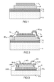
- a typical MIM capacity structure comprises a so-called functional dielectric layer DF sandwiched between two electrodes Es and Ei, the lower electrode being on the surface of a substrate S covered with an insulating layer Ci as illustrated in FIG. figure 1 .
- This insulating dielectric may be a silicon oxide SiO 2 deposited by PECVD, by spraying, or by a spin coating commonly identified by the acronym "SOG” for "Spin On Glass” for example. It can also be a silicon nitride Si x N y deposited by PECVD, LPCVD for example, it could equally well be other insulating materials such as the following compounds: Ta 2 O 5 , Al 2 O 3 , MgO , AIN ...
- a constraint for this dielectric insulation DI is that it must not interfere with the operation of the functional dielectric DF. In particular, he It is important that the capacity that he adds in parallel on the device is negligible compared to the functional capacity. To do this, the state of the art uses an insulating dielectric DI of low dielectric constant with respect to the functional dielectric DF.
- the functional dielectric DF is Pb (Zr, Ti) O 3 (PZT) whose dielectric constant is typically 1000
- PZT Pb (Zr, Ti) O 3
- DI dielectric insulation
- the capacity added by the SiO 2 will be much lower than the capacity of PZT, given equivalent area.
- the use of the dielectric insulation DI can pose a problem of reliability. Indeed, Bouyssou et al. (thesis Emilien Bouyssou, p.20, thesis of the University of Tours, 2006 ), have observed that the SiO 2 used as dielectric insulation DI is at the origin of the appearance of fragility in PZT capacitors, more precisely of premature aging of the capacitors in constant voltage stress test. . This is explained by the hydrogenated compounds used in the CVD deposits of dielectric insulation DI, the method most commonly used in industry and particularly illustrated in figure 3 , coated with a USG (for "Undoped Silicon Glass") layer with Rc contact recovery.
- USG for "Undoped Silicon Glass
- the present invention relates to an integrated capacitance type component using an electrical insulation dielectric not having the aforementioned drawbacks and whose manufacturing process proves to be particularly interesting.
- the electrical insulating material is disposed on or under the upper electrode.
- the crystallized functional dielectric material is an oxide among the following oxides: Pb (Sr, Ti) O 3 , SrTiO 3 , (Ba, Sr) TiO 3 , (Pb, La) (Zr, Ti O 3 , Pb (Mg, Nb, Ti) O 3 , Pb (Zn, Nb, Ti) O 3 , BiFeO 3 , BaTiO 3 .
- the amorphous electrical insulating dielectric material is an oxide among the following oxides: PZT, SrTiO 3 , (Ba, Sr) TiO 3 , (Pb, La) (Zr, Ti) O 3 , Pb ( Mg, Nb, Ti) O 3 , Pb (Zn, Nb, Ti) O 3 , BiFeO 3 , BaTiO 3 .
- the functional dielectric materials and electrical insulator are of the same chemical composition.
- the electrodes are platinum or ruthenium, or ruthenium oxide, or iridium, or iridium oxide, or gold.
- the substrate is made of silicon and comprises a top layer of oxide.
- the capacitance further comprises a bonding layer between the substrate and the lower electrode layer.
- the crystallization is carried out by rapid annealing (RTA).
- RTA rapid annealing
- the present invention proposes, advantageously, the use of a sol-gel type method in a mode that can appear as a "degraded" mode that does not give crystallized layers for the amorphous material, since the production of the latter is stopped after the calcination step, without performing the crystallization step, which requires an annealing operation at a higher temperature.
- a sol-gel process making it possible to produce components having a high permittivity dielectric layer and a layer of material having a lower permittivity ensuring an electrical isolation function between the two types of material. said lower and upper electrodes.
- sol gel method In the case of materials with a very high permittivity, a known technique is the sol gel method and in particular of the sol-gel polymerization type.
- the sol-gel deposition of PbTiO 3 (PT) was reported for the first time in 1984 by GURKOVICH SR, Blum JB, Preparation of monolithic lead-titanate by sol-gel process, in Ultrastructure Processing of Ceramics, Glasses and Composites, LLHa.DR Ulrich, Editor, Wiley-Interscience: New-York, 152-160, 1984 .
- the principle of the sol-gel process is based on a succession of hydrolysis-condensation reactions, at a temperature close to ambient, which leads to the formation of a mineral polymer, which can then be heat-treated.
- the hydrolysis step of the metal alkoxides is schematized by the following reaction: M-OR + H 2 O ⁇ M-OH + ROH where M is a metal cation, and R is an alkyl organic group.
- M is a metal cation
- R is an alkyl organic group.
- This reaction allows the conversion of alkoxy functions to hydroxy function.
- the solution obtained is called soil; that is to say a solid phase, consisting of small entities, dispersed in a liquid (the solvent).
- the hydroxyl functions are then converted into MOM species corresponding to the formation of a mineral macromolecular network constituting the gel.
- the production of piezoelectric films by the sol-gel technique consists of a succession of stages of spreading of the sol-gel solution and heat treatments, as diagrammed below:
- the solution is usually spread on a substrate by centrifugal coating.
- the deposited film thickness depends mainly on the speed of rotation of the spin and the physicochemical parameters of the solution (viscosity, concentration, evaporation rate).
- a drying step makes it possible to evaporate part of the solvents and to obtain a solid deposit.
- the layer then undergoes pyrolysis (or calcination) to remove organic residues.
- This step is crucial because it greatly conditions the structural quality of the piezoelectric film.
- the calcination temperature must be sufficiently high in order to eliminate all the organic residues (typically between 300 ° C. and 450 ° C.). Otherwise, the trapping of organic matter can lead to the presence of porosities. However, too high a temperature may favor the appearance of parasitic phase, such as pyrochlore in the case of PZ, described in the publication: GONG W., L JF, CHU X., Li L., J. Eur. Ceram. Soc. 24, 2977-2982, 2004 .
- the amorphous layer obtained is crystallized and densified at a temperature of between 600 ° C. and 800 ° C.
- This crystallization step is most often carried out by rapid annealing RTA acronym for the name "Rapid Thermal Annealing", rather than by conventional annealing, in particular to limit the thermal budget.
- the fast annealing RTA process is today one of the most used for the crystallization of thin films. Its main asset is a transmission of thermal energy by radiation and not by convection. The result is extremely fast temperature rise of up to 300 ° C / s thanks to the use of halogen lamps. The anneals last a few tens of seconds.
- the thickness of a layer after crystallization is generally about 50 nm.
- the crystallization step is often performed every two or three pyrolyzed layers.
- the advantage of using the RTA process is then understood in order to reduce both the thermal budget and the production time of the films.
- the sol-gel process has the advantage of being inexpensive and relatively simple to implement, requiring only a spreading strip, hot plates and an RTA oven. In addition, it does not require significant maintenance, which is a significant advantage over vacuum deposition techniques. It is also very flexible for the development of complex materials. It is thus easy to vary the compositions by means of the organometallic precursor assay, or to incorporate dopants to optimize the properties of the films.
- the sol gel deposited material undergoes several steps. After pyrolysis, the material was stripped of all its organic compounds (thus H and C). The resulting material is therefore exclusively composed of inorganic materials after this pyrolysis (sometimes called calcination). As the material is not crystallized, it does not have a very high dielectric constant.
- the present invention proposes to exploit this property of lower dielectric constant to use this layer called calcined or pyrolyzed, as DI isolation dielectric as illustrated in FIG. figure 2 .
- This has the advantage of making it possible to use a single material such as dielectric insulation DI and dielectric functional diode DF, the dielectric insulation DI does not have any hydrogenated compounds capable of damaging the properties of the functional dielectric DF, the dielectric constant the insulation dielectric DI remains low compared to that of the functional dielectric DF (typically for the PZT, the dielectric constant of the non-crystallized calcined PZT is between 20 and 30, whereas the dielectric constant of the crystallized PZT is between 400 and 1500 ).
- the integrated capacitor according to the invention comprises, in this example, a functional dielectric material of the perovskite type having a high dielectric constant which may notably be PZT and an amorphous perovskite-type dielectric type electrical insulator which has not undergone a final phase of annealing of crystallization, between the lower electrode and the upper electrode, as illustrated in FIG. figure 5 which shows a possible stack for an integrated capacitance of very high value using PZT as insulating dielectric di am (calcined) and DF functional dielectric cry (crystallized), from a substrate S 0 covered with a layer of oxide S 1 and an adhesion layer C ac and having a lower electrode Ei and an upper electrode Es.
- a functional dielectric material of the perovskite type having a high dielectric constant which may notably be PZT and an amorphous perovskite-type dielectric type electrical insulator which has not undergone a final phase of annealing of crystallization, between the
- a silicon substrate S 0 typically 200mm in diameter.
- An oxidation step is carried out defining a surface layer S 1 of SiO 2 with a thickness of 500 nm, as illustrated in FIG. figure 6a . This prevents diffusion to the substrate.
- a bonding layer C ac made by sputtering 5 nm Ti titanium followed by a rapid annealing oxidation of 2 is then carried out. minutes at 750 ° C under oxygen O 2 .
- This tie layer can also be made tantaleTa.
- the lower electrode Ei is deposited as illustrated in FIG. figure 6b in Pt (100nm) by spraying.
- This electrode can also be made of iridium.
- the lower electrode may or may not be etched for example by ion milling in a suitable pattern.
- the functional dielectric in PZT is made by sol-gel method as evoked according to the reaction scheme previously described, referenced DF Cree and illustrated in FIG. Figure 6c .
- 200 nm of PZT can be deposited by at least one spin coating, followed by a drying operation at 110 ° C. for 5 minutes on a heating plate, and a pyrolysis step at 350 ° C. C for 5 minutes on a hotplate.
- each deposition is followed by a drying and pyrolysis operation before the next deposition.
- the PZT is then etched by a so-called wet process based on the following preparation: 1% HF, 37% HCl in water and in the following relative proportions: 5/9/50.
- This etching can also be done by dry etching using a RIE (Reactive Ion Etching) equipment with chlorine type gases with argon addition as illustrated in FIG. figure 6d .
- the definition of this etching is done by using prior to etching a photosensitive resin defined by a photolithography step using a dedicated mask.
- the sputtering electrode Es is then deposited in Pt, typically 100 nm thick, as illustrated in FIG. figure 6e .
- This electrode can be just as well as ruthenium, or ruthenium oxide, iridium, or iridium oxide, or even gold.
- This electrode is etched by ionic machining. The definition of this engraving by using prior to etching a photosensitive resin defined by a photolithography step using a dedicated mask.
- the insulating dielectric is then deposited by a gel sol method but by not doing the final crystallization step, referenced D1 am and illustrated in FIG. figure 6f .
- PZT or other materials which may especially be SrTiO 3 , (Ba, Sr) TiO 3 , (Pb, La) (Zr, Ti) O 3 , Pb (Mg, Nb, Ti) O 3 , Pb (Zn, Nb, Ti) O 3 , BiFeO 3 , BaTiO 3 ).
- the insulation dielectric layer may have a thickness of about 400 nm, obtained by six calcined deposits made by spin coating, followed by a drying operation at 110 ° C.
- This insulating dielectric is then etched by wet process based on the preparation HF 1% - HCl 37% - H 2 O in the proportions 5/9/200.
- the definition of this etching is done by using prior to etching a photosensitive resin defined by a photolithography step using a dedicated mask as illustrated in FIG. figure 6g .
- a metal is then deposited to make the contact resumption Rc as illustrated in FIG. figure 6h .
- This metal may be in a nonlimiting manner Al, Al / Cu, Al / Si, Cu, Pt .... It is especially possible to use an Al / Cu1% alloy over 1 ⁇ m of aluminum. thickness, deposited by spraying.
- This layer is then etched by wet or dry process as illustrated in figure 6i .
- the definition of this etching is done by using prior to etching a photosensitive resin defined by a photolithography step using a dedicated mask.
- an insulating protective layer I is deposited as illustrated in FIG. figure 6j , which is etched to access the contact layer Rc as illustrated in FIG. figure 6k .
Landscapes
- Semiconductor Memories (AREA)
- Semiconductor Integrated Circuits (AREA)
- Engineering & Computer Science (AREA)
- Power Engineering (AREA)
- Chemical & Material Sciences (AREA)
- Materials Engineering (AREA)
Abstract
Description
- Le domaine de l'invention est celui des composants de type capacité intégrée comprenant une couche de diélectrique comprise entre une électrode supérieure et une électrode inférieure et avec reprise de contact, nécessitant l'utilisation d'isolant électrique entre les deux types d'électrodes.
- Typiquement ce type de composant peut être utilisé dans le cadre d'actionneurs piézoélectriques, notamment pour l'optique adaptative ou des actionneurs pour imprimantes à jet d'encre. De tels composants peuvent également être utilisés pour réaliser des résonateurs et des filtres radiofréquences acoustiques utilisant un effet piézoélectrique pour la téléphonie mobile. Ils sont également intéressants pour l'élaboration de capacités variables ferroélectriques, de capacités à très fortes valeurs utilisées pour la téléphonie mobile ou les objets nomades en général (pacemaker, objets communicants).
- Actuellement pour réaliser des capacités intégrées en technologie plane (appelée MIM pour Métal Isolant Métal), on a besoin de reprendre les contacts électriques sur les électrodes. En effet, une structure typique de capacité MIM comporte une couche de diélectrique dit fonctionnel DF en sandwich entre deux électrodes Es et Ei, l'électrode inférieure étant à la surface d'un substrat S recouvert d'une couche isolante Ci comme illustré en
figure 1 . - Pour reprendre les contacts via une couche de reprise de contacts RCsup et RCinf, et pour éviter le court circuit entre les électrodes supérieure et inférieure, il est nécessaire d'utiliser un diélectrique d'isolation DI comme illustré sur la
figure 2 . - Ce diélectrique d'isolation peut être un oxyde de silicium SiO2 déposé par PECVD, par pulvérisation, ou par un dépôt à la tournette couramment identifié par l'acronyme « SOG » pour « Spin On Glass » par exemple. Cela peut être aussi un nitrure de silicium SixNy déposé par PECVD, LPCVD par exemple, il pourrait tout aussi bien s'agir d'autres matériaux isolants tels que les composés suivants : Ta2O5, Al2O3, MgO, AIN...
- Une contrainte pour ce diélectrique d'isolation DI est qu'il ne doit pas perturber le fonctionnement du diélectrique fonctionnel DF. En particulier, il est important que la capacité qu'il rajoute en parallèle sur le dispositif soit négligeable par rapport à la capacité fonctionnelle. Pour ce faire, l'état de l'art utilise un diélectrique d'isolation DI de constante diélectrique faible par rapport au diélectrique fonctionnel DF.
- Par exemple, si le diélectrique fonctionnel DF est du Pb(Zr,Ti)O3 (PZT) dont la constante diélectrique vaut typiquement 1000, il est courant d'utiliser un oxyde de silicium comme diélectrique d'isolation DI dont la constante diélectrique vaut 4. Ainsi, la capacité ajoutée par le SiO2 sera beaucoup plus faible que la capacité de PZT, à surface équivalente donnée.
- Pour le PZT et autres oxydes à très forte permittivité, l'utilisation du diélectrique d'isolation DI peut poser un problème de fiabilité. En effet, Bouyssou et al. (thèse Emilien Bouyssou, p.20, thèse de l'Université de Tours, 2006), ont observé que le SiO2 utilisé comme diélectrique d'isolation DI est à l'origine de l'apparition d'une fragilité dans des capacités de PZT, plus précisément d'un vieillissement prématuré des condensateurs en test de contrainte en tension constante. Ceci est expliqué par les composés hydrogénés utilisés lors des dépôts CVD des diélectriques d'isolation DI, méthode la plus couramment utilisée dans l'industrie et notamment illustré en
figure 3 , recouvert d'une couche USG (pour « Undoped Silicon Glass) avec reprise de contact Rc. - Dans ce contexte, la présente invention a pour objet un composant de type capacité intégrée utilisant un diélectrique d'isolation électrique ne présentant pas les inconvénients précités et dont le procédé de fabrication s'avère être particulièrement intéressant.
- Plus précisément la présente invention a pour objet une capacité intégrée comprenant une couche de matériau diélectrique dit fonctionnel à base de matériau cristallisé de type pérovskite, comprise entre au moins une première électrode dite inférieure à la surface d'un substrat et au moins d'une deuxième électrode dite supérieure, lesdites électrodes étant isolées électriquement par une couche de matériau isolant électrique pour permettre au moins une reprise de contact sur l'électrode supérieure, caractérisée en ce que :
- le matériau isolant électrique est en matériau diélectrique amorphe de type pérovskite présentant une constante diélectrique inférieure à celle du matériau cristallisé de type pérovskite et
- la reprise de contact est formée à partir d'une couche de reprise de contact gravée en contact avec la couche de diélectrique isolant électrique au niveau de sa surface parallèle au plan des couches.
- Selon une variante de l'invention, le matériau isolant électrique est disposé sur ou sous l'électrode supérieure.
- Selon une variante de l'invention, le matériau diélectrique fonctionnel cristallisé est un oxyde parmi les oxydes suivants : Pb(Sr,Ti)O3, SrTiO3, (Ba,Sr)TiO3, (Pb,La)(Zr,Ti)O3, Pb(Mg,Nb,Ti)O3, Pb(Zn,Nb,Ti)O3, BiFeO3, BaTiO3.
- Selon une variante de l'invention, le matériau diélectrique isolant électrique amorphe est un oxyde parmi les oxydes suivants : PZT, SrTiO3, (Ba,Sr)TiO3, (Pb,La)(Zr,Ti)O3, Pb(Mg,Nb,Ti)O3, Pb(Zn,Nb,Ti)O3, BiFeO3, BaTiO3.
- Selon une variante de l'invention, les matériaux diélectriques fonctionnel et isolant électrique sont de même composition chimique.
- Selon une variante de l'invention, les électrodes sont en platine ou en ruthénium, ou en oxyde de ruthénium, ou en iridium, ou en oxyde d'iridium, ou en or.
- Selon une variante de l'invention, le substrat est en silicium et comporte une couche supérieure d'oxyde.
- Selon une variante de l'invention, la capacité comporte en outre une couche d'accrochage entre le substrat et la couche d'électrode inférieure.
- L'invention a aussi pour obet un procédé de fabrication d'une capacité intégrée selon l'invention, caractérisé en ce qu'il comprend au moins une étape de réalisation d'une couche de matériau diélectrique amorphe et isolant électrique, au dessus ou au dessous de l'électrode supérieure, par procédé sol-gel comportant :
- l'étalement d'une solution sol-gel ;
- le séchage de ladite solution à une température comprise entre environ 100°C et 150°C ;
- la pyrolyse de ladite solution séchée à une température comprise entre environ 300°C et 500°C conduisant au matériau diélectrique isolant amorphe.
- Selon une variante de l'invention, le procédé comprend au moins :
- une étape de réalisation d'une couche de matériau diélectrique fonctionnel cristallisé (DFcris) entre l'électrode inférieure et l'électrode supérieure par procédé sol-gel comportant :
- l'étalement d'une solution sol-gel à la surface d'un substrat comportant une électrode inférieure ;
- le séchage de ladite solution à une température comprise entre environ 100°C et 150°C;
- la pyrolyse de ladite solution séchée à une température comprise entre environ 300°C et 500°C conduisant à un matériau diélectrique fonctionnel amorphe;
- la cristallisation dudit matériau fonctionnel amorphe porté à une température supérieure ou égale à la température de cristallisation dudit matériau de manière à obtenir le matériau diélectrique fonctionnel cristallisé (DFcris).
- Selon une variante de l'invention, la cristallisation est effectuée par recuit rapide (RTA).
- Ainsi la présente invention propose notamment avantageusement d'utiliser un procédé de type sol-gel dans un mode pouvant apparaître comme un mode « dégradé » ne donnant pas de couches cristallisées pour le matériau amorphe, puisque la réalisation de ce dernier, s'arrête après l'étape de calcination, sans réaliser l'étape de cristallisation, qui requière une opération de recuit à plus haute température.
- L'invention sera mieux comprise et d'autres avantages apparaîtront à la lecture de la description qui va suivre donnée à titre non limitatif et grâce aux figures annexées parmi lesquelles :
- la
figure 1 illustre un exemple de structure capacité MIM selon l'art connu ; - la
figure 2 illustre un exemple d'utilisation d'un diélectrique d'isolation pour reprendre les contacts sur la capacité MIM selon l'art connu ; - la
figure 3 illustre l'apparition de défauts dans le PZT, dus à la présence d'hydrogène dans un verre non dopé de silice ; - les
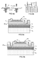
figures 4a et 4b illustrent deux exemples de procédés d'étalement de type sol-gel sur un substrat par enduction centrifuge et par trempage-retrait ; - les
figures 5a et 5b illustrent un exemple d'empilement pour une capacité à forte permittivité selon l'invention avec électrode inférieure non gravée ou gravée ; - les étapes 6a à 6k illustrent les différentes étapes d'un procédé de fabrication d'une capacité intégrée selon l'invention.
- Selon l'invention, il est proposé d'utiliser un procédé sol-gel permettant de réaliser des composants présentant une couche diélectrique de forte permittivité et une couche de matériau ayant une permittivité plus faible assurant une fonction d'isolation électrique entre les deux types d'électrodes dite inférieure et supérieure.
- Dans le cas de matériaux à très forte permittivité, une technique connue est le procédé sol gel et notamment de type polymérisation sol-gel. Le dépôt par voie sol-gel de PbTiO3 (PT) a été rapporté pour la première fois en 1984 par GURKOVICH S. R., Blum J. B., Preparation of monolithic lead-titanate by sol-gel process, in Ultrastructure Processing of Ceramics, Glasses and Composites, L.L.Ha.D.R. Ulrich, Editor, Wiley-Interscience: New-York, 152-160, 1984.
- L'année suivante, Budd ans al. BUDD K. D., Dey S. K., PAYNE D. A., Sol-gel processing of PT, PZ, PZT and PLZT thin films. Br. Ceram. Proc. 107-121, 1985, ont décrit la synthèse de films minces pérovskites à base de plomb (PT, PZ, PZT, PLZT)]. Ce procédé utilise une solution contenant des précurseurs réactifs tels que les sels métalliques ou les alcoxydes, et un solvant. Le dépôt des couches minces peut se faire par enduction centrifuge (spin-coating) ou bien par trempage-retrait (dip-coating) comme illustré sur les
figures 4a et 4b . - Le principe du procédé sol-gel repose sur une succession de réactions d'hydrolyse-condensation, à une température proche de l'ambiante, qui conduit à la formation d'un polymère minéral, lequel peut ensuite être traité thermiquement. L'étape d'hydrolyse des alcoxydes métalliques est schématisée par la réaction suivante :
M-OR + H2O → M-OH + ROH
où M est un cation métallique, et R un groupe organique alkyl. Cette réaction permet la conversion des fonctions alcoxy en fonction hydroxy. La solution obtenue est appelée sol ; c'est-à-dire une phase solide, constituée de petites entités, dispersée dans un liquide (le solvant). Les fonctions hydroxy sont ensuite converties en espèces M-O-M correspondant à la formation d'un réseau macromoléculaire minéral constituant le gel. Cela se fait suivant plusieurs réactions de condensation (formation de ponts oxo, -O-, par réactions d'oxolation) avec élimination d'alcool et d'eau.
M-OH + M-OR → M-O-M + ROH
M-OH + M-OH → M-O-M + H20
- La réalisation des films piézoélectriques par la technique sol-gel consiste en une succession d'étapes d'étalement de la solution sol-gel et de traitements thermiques, comme schématisé ci-après :

- La solution est habituellement étalée sur un substrat par enduction centrifuge. L'épaisseur de film déposée dépend principalement de la vitesse de rotation de la tournette et des paramètres physico-chimiques de la solution (viscosité, concentration, taux d'évaporation). Une étape de séchage permet d'évaporer une partie des solvants et d'obtenir un dépôt solide. La couche subit ensuite une pyrolyse (ou calcination) afin d'éliminer les résidus organiques.
- Cette étape, généralement effectuée sur plaque chauffante, est cruciale car elle conditionne grandement la qualité structurale du film piézoélectrique. La température de calcination doit être suffisamment élevée afin d'éliminer la totalité des résidus organiques (typiquement comprise entre 300°C et 450°C). Dans le cas contraire, le piégeage de matière organique peut conduire à la présence de porosités. Cependant, une température trop élevée risque de favoriser l'apparition de phase parasite, comme la pyrochlore dans le cas du PZ, décrit dans la publication : GONG W., L J. F., CHU X., Li L., J. Eur. Ceram. Soc. 24, 2977-2982, 2004.
- Après pyrolyse, la couche amorphe obtenue est cristallisée et densifiée à une température comprise entre 600°C et 800°C. Cette étape de cristallisation est le plus souvent réalisée par recuit rapide RTA acronyme de l'appelation « Rapid Thermal Annealing », plutôt que par recuit conventionnel, afin notamment de limiter le budget thermique. Le procédé de recuit rapide RTA est aujourd'hui parmi les plus utilisés pour la cristallisation des films minces. Son principal atout est une transmission de l'énergie thermique par rayonnement et non par convection. Il en résulte des montées en température extrêmement rapide pouvant atteindre jusqu'à 300°C/s grâce à l'utilisation de lampes halogènes. Les recuits durent quelques dizaines de secondes. L'épaisseur d'une couche après cristallisation est généralement d'environ 50 nm. Suivant l'épaisseur finale de matériau désirée, il faut répéter à plusieurs reprises l'ensemble des étapes précédemment décrites. Toutefois, l'étape de cristallisation est bien souvent effectuée toutes les deux ou trois couches pyrolysées. On comprend alors l'intérêt d'utiliser le procédé RTA afin de réduire à la fois le budget thermique et le temps de fabrication des films.
- Le procédé sol-gel présente l'avantage d'être peu onéreux et relativement simple à mettre en oeuvre, ne nécessitant qu'une piste d'étalement, des plaques chauffantes et un four RTA. De plus, il ne requiert pas une maintenance importante, ce qui est un atout non négligeable par rapport aux techniques de dépôt sous vide. Il est par ailleurs très flexible pour le développement de matériaux complexes. On peut ainsi facilement faire varier les compositions par le biais du dosage des précurseurs organométalliques, ou bien incorporer des dopants pour optimiser les propriétés des films.
- De manière générale, le matériau déposé par procédé sol gel subit plusieurs étapes. Après pyrolyse, le matériau a été débarrassé de tous ses composés organiques (donc H et C). Le matériau résultant est donc exclusivement composé de matières non organiques après cette pyrolyse (parfois appelé calcination). Comme le matériau n'est pas cristallisé, il ne possède pas de constante diélectrique très élevée.
- La présente invention propose d'exploiter cette propriété de plus faible constante diélectrique pour utiliser cette couche appelée calcinée ou pyrolysée, comme diélectrique d'isolation DI comme illustré en
figure 2 . Cela présente l'avantage de permettre d'utiliser un matériau unique comme diélectrique d'isolation DI et diélectrique fonctionnel DF, le diélectrique d'isolation DI ne possède pas de composés hydrogénés susceptibles d'abimer les propriétés du diélectrique fonctionnel DF, la constante diélectrique du diélectrique d'isolation DI reste faible comparée à celle du diélectrique fonctionnel DF (typiquement pour le PZT, la constante diélectrique du PZT calciné non cristallisé se situe entre 20 et 30, alors que la constante diélectrique du PZT cristallisé se situe entre 400 et 1500). - La capacité intégrée selon l'invention comprend dans cet exemple un matériau diélectrique fonctionnel de type pérovskite présentant une constante diélectrique élevée pouvant notamment être du PZT et un isolant électrique de type diélectrique de type pérovskite amorphe n'ayant pas subi de phase finale de recuit de cristallisation, entre l'électrode inférieure et l'électrode supérieure, comme illustré en
figure 5 qui montre un empilement possible pour une capacité intégrée de très forte valeur utilisant du PZT comme diélectrique d'isolation DIam (calciné) et diélectrique fonctionnel DFcris (cristallisé), à partir d'un substrat S0 recouvert d'une couche d'oxyde S1 et d'une couche d'accrochage Cac et comportant une électrode inférieure Ei et une électrode supérieure Es. - Les différentes étapes du procédé sont décrites ci-après à l'aide des
figures 6a à 6k . - Pour réaliser un tel empilement, on peut utiliser un substrat silicium S0, typiquement de 200mm de diamètre. On procède à une étape d'oxydation définissant une couche surfacique S1 de SiO2 d'épaisseur de 500nm, comme illustré en
figure 6a . Cela permet de prévenir les diffusions vers le substrat. - On réalise alors le dépôt d'une couche d'accroche Cac faite par pulvérisation de 5nm de titane Ti suivi d'une oxydation par recuit rapide de 2 minutes à 750°C sous oxygène O2. Cette couche d'accroche peut être également faite en tantaleTa.
- On réalise le dépôt de l'électrode inférieure Ei comme illustré en
figure 6b , en Pt (100nm) par pulvérisation. Cette électrode peut également être en iridium. L'électrode inférieure peut ou non être gravée par exemple par usinage ionique selon un motif approprié. - On procède à la réalisation du diélectrique fonctionnel en PZT par procédé sol gel comme évoqué selon le schéma réactionnel précédemment décrit, référencé DFcris et illustré en
figure 6c . Typiquement, on peut déposer 200 nm de PZT en faisant au moins un dépôt à la tournette, suivi d'une d'opération de séchage à 110°C durant 5 minutes sur une plaque chauffante, et d'une étape de pyrolyse à 350°C durant 5 minutes sur plaque chauffante. Dans le cas de l'utilisation de dépôt successifs pour obtenir l'épaisseur souhaité de PZT, chaque dépôt est suivi d'une opération de séchage et de pyrolyse avant le dépôt suivant . - On procède alors à une opération de recuit final de cristallisation à 700°C sous air pendant 30 secondes. Généralement ce recuit doit-être réalisé tous les 3 (dépôt/séchage/ pyrolyse) de PZT.
- Il est possible d'utiliser d'autres matériaux que le PZT, à très forte permittivité pouvant être notamment l'un des oxydes suivants : SrTiO3, (Ba,Sr)TiO3, (Pb,La)(Zr,Ti)O3, Pb(Mg,Nb,Ti)O3, Pb(Zn,Nb,Ti)O3, BiFeO3, BaTiO3.
- Le PZT est ensuite gravé par un procédé dit humide à base de la préparation suivante : HF à 1%, HCl à 37% dans de l'eau et dans les proportions relatives suivantes : 5/ 9/ 50. Cette gravure peut également être faire par gravure sèche en utilisant un équipement de RIE (Reactive Ion Etching) avec des gaz de type chloré avec adjonction d'argon comme illustré en
figure 6d . La définition de cette gravure se fait en utilisant préalablement à la gravure une résine photosensible définie par une étape de photolithographie en utilisant un masque dédié. - On procède alors au dépôt par pulvérisation de l'électrode supérieure Es en Pt d'épaisseur typiquement de 100nm comme illustré en
figure 6e . Cette électrode peut être tout aussi bien être en ruthénium, ou oxyde de ruthénium, en iridium, ou en oxyde d'iridium, ou bien encore en or. Cette électrode est gravée par usinage ionique. La définition de cette gravure se fait en utilisant préalablement à la gravure une résine photosensible définie par une étape de photolithographie en utilisant un masque dédié. - On dépose ensuite le diélectrique d'isolation par procédé sol gel mais en ne faisant pas l'étape finale de cristallisation, référencé Dlam et illustré en
figure 6f . Dans ce cas, on utilise du PZT ou d'autres matériaux pouvant notamment être du SrTiO3, (Ba,Sr)TiO3, (Pb,La)(Zr,Ti)O3, Pb(Mg,Nb,Ti)O3, Pb(Zn,Nb,Ti)O3, BiFeO3, BaTiO3). Typiquement la couche de diélectrique d'isolation peut avoir une épaisseur de l'ordre de 400nm environ, obtenue par six dépôts calcinés réalisés par dépôts à la tournette, suivis d'une opération de séchage à 110°C pendant 5 minutes sur plaque chauffante, suivie d'une opération de pyrolyse à 350°C durant 5 minutes sur plaque chauffante, réitérée six fois. Il est possible de diminuer ou d'augmenter l'épaisseur en réduisant ou en augmentant le nombre de dépôt (dépôt tournette + séchage à 110°C durant 5minutes sur plaque chauffante + pyrolyse à 350°C durant 5 minutes sur plaque chauffante) ou la viscosité du liquide sol gel. - Ce diélectrique d'isolation est ensuite gravé par procédé humide à base de la préparation HF 1% - HCl 37% - H2O dans les proportions 5/9/200 . La définition de cette gravure se fait en utilisant préalablement à la gravure une résine photosensible définie par une étape de photolithographie en utilisant un masque dédié comme illustré en
figure 6g . - On dépose ensuite un métal pour faire la reprise de contact Rc comme illustré en
figure 6h . Ce métal peut être de manière non limitative de l'Al, de l'Al/Cu, de l'Al/Si, du Cu, du Pt....On peut notamment utiliser un alliage Al/Cu1% sur 1µm d'épaisseur, déposé par pulvérisation. - Cette couche est ensuite gravée par procédé humide ou sec comme illustré en
figure 6i . La définition de cette gravure se fait en utilisant préalablement à la gravure une résine photosensible définie par une étape de photolithographie en utilisant un masque dédié. - On dépose enfin une couche isolante de protection I comme illustré en
figure 6j , qui est gravée afin d'accéder à la couche de contact Rc comme illustré enfigure 6k .
Claims (11)
- Capacité intégrée comprenant une couche de matériau diélectrique dit fonctionnel (DFcris) à base de matériau cristallisé de type pérovskite, comprise entre au moins une première électrode dite inférieure (Ei) à la surface d'un substrat et au moins d'une deuxième électrode dite supérieure (Es), lesdites électrodes étant isolées électriquement par une couche de matériau isolant électrique pour permettre au moins une reprise de contact sur l'électrode supérieure, caractérisée en ce que :- le matériau isolant électrique est en matériau diélectrique amorphe de type pérovskite (DIam) présentant une constante diélectrique inférieure à celle du matériau cristallisé de type pérovskite et- la reprise de contact est formée à partir d'une couche de reprise de contact (Rc) gravée en contact avec la couche de diélectrique isolant électrique au niveau de sa surface parallèle au plan des couches.
- Capacité intégrée selon la revendication 1, caractérisée en ce que le matériau isolant électrique est disposé sur ou sous l'électrode supérieure.
- Capacité intégrée selon l'une des revendications 1 ou 2, caractérisée en ce que le matériau diélectrique fonctionnel cristallisé est un oxyde parmi les oxydes suivants : Pb(Sr,Ti)O3, SrTiO3, (Ba,Sr)TiO3, (Pb,La)(Zr,Ti)O3, Pb(Mg,Nb,Ti)O3, Pb(Zn,Nb,Ti)O3, BiFeO3, BaTiO3.
- Capacité intégrée selon l'une des revendications 1 à 3, caractérisée en ce que le matériau diélectrique isolant électrique amorphe est un oxyde parmi les oxydes suivants : PZT, SrTiO3, (Ba,Sr)TiO3, (Pb,La)(Zr,Ti)O3, Pb(Mg,Nb,Ti)O3, Pb(Zn,Nb,Ti)O3, BiFeO3, BaTiO3.
- Capacité intégrée selon l'une des revendications 1 à 4, caractérisé en ce que les matériaux diélectriques fonctionnel et isolant électrique sont de même composition chimique.
- Capacité intégrée selon l'une des revendications 1 à 5, caractérisée en ce que les électrodes sont en platine ou en ruthénium, ou en oxyde de ruthénium, ou en iridium, ou en oxyde d'iridium, ou en or.
- Capacité intégrée selon l'une des revendications 1 à 6, caractérisée en ce que le substrat est en silicium (S0) et comporte une couche supérieure d'oxyde (S1).
- Capacité intégrée selon l'une des revendications 1 à 7, caractérisée en ce qu'elle comporte en outre une couche d'accrochage entre le substrat et la couche d'électrode inférieure (Cac).
- Procédé de fabrication d'une capacité intégrée selon l'une des revendications 1 à 8, caractérisé en ce qu'il comprend au moins une étape de réalisation d'une couche de matériau diélectrique amorphe et isolant électrique (Dl am), au dessus ou au dessous de l'électrode supérieure, par procédé sol-gel comportant :- l'étalement d'une solution sol-gel ;- le séchage de ladite solution à une température comprise entre environ 100°C et 150°C ;- la pyrolyse de ladite solution séchée à une température comprise entre environ 300°C et 500°C conduisant au matériau diélectrique isolant amorphe (Dlam).
- Procédé de fabrication d'une capacité intégrée selon la revendication 9, caractérisé en ce qu'il comprend au moins une étape de réalisation d'une couche de matériau diélectrique fonctionnel cristallisé (DFcris) entre l'électrode inférieure et l'électrode supérieure par procédé sol-gel comportant :- l'étalement d'une solution sol-gel à la surface d'un substrat comportant une électrode inférieure ;- le séchage de ladite solution à une température comprise entre environ 100°C et 150°C ;- la pyrolyse de ladite solution séchée à une température comprise entre environ 300°C et 500°C conduisant à un matériau diélectrique fonctionnel amorphe;- la cristallisation dudit matériau fonctionnel amorphe porté à une température supérieure ou égale à la température de cristallisation dudit matériau de manière à obtenir le matériau diélectrique fonctionnel cristallisé (DFcris).
- Procédé de fabrication d'une capacité intégrée selon la revendication 10, caractérisé en ce que la cristallisation est effectuée par recuit rapide (RTA).
Applications Claiming Priority (1)
| Application Number | Priority Date | Filing Date | Title |
|---|---|---|---|
| FR1003527A FR2964497B1 (fr) | 2010-09-03 | 2010-09-03 | Capacité intégrée comprenant une couche d'isolation électrique en matériau de type perovskite amorphe et procédé de fabrication |
Publications (2)
| Publication Number | Publication Date |
|---|---|
| EP2426698A1 true EP2426698A1 (fr) | 2012-03-07 |
| EP2426698B1 EP2426698B1 (fr) | 2022-09-28 |
Family
ID=43589620
Family Applications (1)
| Application Number | Title | Priority Date | Filing Date |
|---|---|---|---|
| EP11178220.7A Active EP2426698B1 (fr) | 2010-09-03 | 2011-08-22 | Capacité intégrée comprenant une couche d'isolation électrique en matériau de type pérovskite amorphe et procédé de fabrication |
Country Status (3)
| Country | Link |
|---|---|
| US (1) | US9673269B2 (fr) |
| EP (1) | EP2426698B1 (fr) |
| FR (1) | FR2964497B1 (fr) |
Families Citing this family (7)
| Publication number | Priority date | Publication date | Assignee | Title |
|---|---|---|---|---|
| FR2951336B1 (fr) | 2009-10-09 | 2017-02-10 | Commissariat Energie Atomique | Dispositif a ondes acoustiques comprenant un filtre a ondes de surface et un filtre a ondes de volume et procede de fabrication |
| FR2968861B1 (fr) | 2010-12-10 | 2013-09-27 | Commissariat Energie Atomique | Procédé de fabrication d'un résonateur a ondes acoustiques comprenant une membrane suspendue |
| FR2974691B1 (fr) | 2011-04-28 | 2019-08-30 | Commissariat A L'energie Atomique Et Aux Energies Alternatives | Dispositif electromecanique a ondes acoustiques comprenant une zone de transduction et une cavite etendue |
| FR2976126B1 (fr) | 2011-06-01 | 2014-05-09 | Commissariat Energie Atomique | Composant electrique comprenant un materiau de structure perovskite et des electrodes optimisees et procede de fabrication |
| CN110885473B (zh) * | 2019-12-09 | 2022-06-17 | 中国科学院深圳先进技术研究院 | 一种纳米颗粒、复合薄膜及其制备方法和应用 |
| US12047744B2 (en) * | 2021-04-26 | 2024-07-23 | Rf360 Singapore Pte. Ltd. | Etch stop and protection layer for capacitor processing in electroacoustic devices |
| CN120473335B (zh) * | 2025-07-16 | 2025-10-21 | 昆山清元电子科技有限公司 | 高压多层薄膜电容器及其制备方法 |
Citations (4)
| Publication number | Priority date | Publication date | Assignee | Title |
|---|---|---|---|---|
| US20010001488A1 (en) * | 1996-08-20 | 2001-05-24 | Eastep Brian Lee | Completely encapsulated top electrode of a ferroelectric capacitor using a lead-enhanced encapsulation layer |
| EP1217658A2 (fr) * | 2000-12-20 | 2002-06-26 | Fujitsu Limited | Méthode de production de films en PZT de haute qualité pour mémoires ferroélectriques de circuits intégrés |
| US20020175361A1 (en) * | 2001-05-22 | 2002-11-28 | Glen Fox | Charge pump or other charge storage capacitor including pzt layer for combined use as encapsulation layer and dielectric layer of ferroelectric capacitor and a method for manufacturing the same |
| US20070196932A1 (en) * | 2006-02-20 | 2007-08-23 | Fujitsu Limited | Method for forming ferroelectric capacitor and method for fabricating semiconductor device |
Family Cites Families (10)
| Publication number | Priority date | Publication date | Assignee | Title |
|---|---|---|---|---|
| US7005695B1 (en) * | 2000-02-23 | 2006-02-28 | Micron Technology, Inc. | Integrated circuitry including a capacitor with an amorphous and a crystalline high K capacitor dielectric region |
| US7011978B2 (en) * | 2001-08-17 | 2006-03-14 | Micron Technology, Inc. | Methods of forming capacitor constructions comprising perovskite-type dielectric materials with different amount of crystallinity regions |
| US7161793B2 (en) * | 2002-11-14 | 2007-01-09 | Fujitsu Limited | Layer capacitor element and production process as well as electronic device |
| WO2006008789A1 (fr) * | 2004-07-15 | 2006-01-26 | Fujitsu Limited | Élément capacitif et son procédé de fabrication, et dispositif semi-conducteur |
| JP2006253631A (ja) * | 2005-02-14 | 2006-09-21 | Fujitsu Ltd | 半導体装置及びその製造方法、キャパシタ構造体及びその製造方法 |
| WO2006117912A1 (fr) * | 2005-04-27 | 2006-11-09 | Murata Manufacturing Co., Ltd | Condensateur a couches minces et son procede de fabrication |
| FR2950197A1 (fr) | 2009-09-15 | 2011-03-18 | Commissariat Energie Atomique | Membrane piezoelectrique a actionnement optimise et procede de fabrication de la membrane |
| FR2951014B1 (fr) | 2009-10-06 | 2011-11-25 | Commissariat Energie Atomique | Structure d'actionnement piezoelectrique comportant une jauge de contrainte piezoresistive integree et son procede de realisation |
| US20110311718A1 (en) * | 2009-12-17 | 2011-12-22 | E.I. Du Pont De Nemours And Company | Method of manufacturing thin-film dielectrics and capacitors on metal foils |
| FR2962613B1 (fr) | 2010-07-06 | 2013-08-16 | Commissariat Energie Atomique | Dispositif d'adaptation d'impedance d'un composant comportant un filtre a impedance adaptable a base de materiau de type perovskite |
-
2010
- 2010-09-03 FR FR1003527A patent/FR2964497B1/fr not_active Expired - Fee Related
-
2011
- 2011-08-22 EP EP11178220.7A patent/EP2426698B1/fr active Active
- 2011-09-04 US US13/225,451 patent/US9673269B2/en active Active
Patent Citations (4)
| Publication number | Priority date | Publication date | Assignee | Title |
|---|---|---|---|---|
| US20010001488A1 (en) * | 1996-08-20 | 2001-05-24 | Eastep Brian Lee | Completely encapsulated top electrode of a ferroelectric capacitor using a lead-enhanced encapsulation layer |
| EP1217658A2 (fr) * | 2000-12-20 | 2002-06-26 | Fujitsu Limited | Méthode de production de films en PZT de haute qualité pour mémoires ferroélectriques de circuits intégrés |
| US20020175361A1 (en) * | 2001-05-22 | 2002-11-28 | Glen Fox | Charge pump or other charge storage capacitor including pzt layer for combined use as encapsulation layer and dielectric layer of ferroelectric capacitor and a method for manufacturing the same |
| US20070196932A1 (en) * | 2006-02-20 | 2007-08-23 | Fujitsu Limited | Method for forming ferroelectric capacitor and method for fabricating semiconductor device |
Non-Patent Citations (6)
| Title |
|---|
| BUDD K. D., DEY S. K., PAYNE D. A.: "Sol-gel processing of PT, PZ, PZT and PLZT thin films", BR. CERAM. PROC., 1985, pages 107 - 121, XP000910602 |
| EMILIEN BOUYSSOU, THÈSE DE L'UNIVERSITÉ DE TOURS, 2006, pages 20 |
| GONG W ET AL: "Effect of pyrolysis temperature on preferential orientation and electrical properties of sol-gel derived lead zirconate titanate films", JOURNAL OF THE EUROPEAN CERAMIC SOCIETY, ELSEVIER SCIENCE PUBLISHERS, BARKING, ESSEX, GB, vol. 24, no. 10-11, 1 September 2004 (2004-09-01), pages 2977 - 2982, XP004504401, ISSN: 0955-2219, DOI: 10.1016/J.JEURCERAMSOC.2003.10.007 * |
| GONG W., L J. F., CHU X., LI L., J. EUR. CERAM. SOC., vol. 24, 2004, pages 2977 - 2982 |
| GURKOVICH S. R., BLUM J. B.: "Ultrastructure Processing of Ceramics, Glasses and Composites", 1984, WILEY-INTERSCIENCE, article "Preparation of monolithic lead- titanate by sol-gel process", pages: 152 - 160 |
| XU Y ET AL: "Electrical characterizations of polycrystalline and amorphous thin films of Pb(ZrxTi1-x)O3 and BaTiO3 prepared by sol-gel technique", JOURNAL OF NON-CRYSTALLINE SOLIDS, NORTH-HOLLAND PHYSICS PUBLISHING. AMSTERDAM, NL, vol. 176, no. 1, 2 October 1994 (1994-10-02), pages 1 - 17, XP024061984, ISSN: 0022-3093, [retrieved on 19941002], DOI: 10.1016/0022-3093(94)90205-4 * |
Also Published As
| Publication number | Publication date |
|---|---|
| EP2426698B1 (fr) | 2022-09-28 |
| US9673269B2 (en) | 2017-06-06 |
| US20120056299A1 (en) | 2012-03-08 |
| FR2964497A1 (fr) | 2012-03-09 |
| FR2964497B1 (fr) | 2013-04-19 |
Similar Documents
| Publication | Publication Date | Title |
|---|---|---|
| EP2426698B1 (fr) | Capacité intégrée comprenant une couche d'isolation électrique en matériau de type pérovskite amorphe et procédé de fabrication | |
| EP1899048B1 (fr) | Revetement de surface hydrophobe et a faible hysteresis de mouillage, procede de depot d'un tel revetement, micro-composant et utilisation | |
| KR20020077203A (ko) | 비휘발성 메모리에 사용되는 지르코늄상의 단일 씨-축납게르마늄산화물 박막과 그 제조방법 | |
| KR20030076927A (ko) | 금속 포일상의 pzt 유전체 박막 조성물 | |
| FR2944147A1 (fr) | Procede de fabrication d'une structure a surfacee externe texturee pour dispositif a diode electroluminescente organique et struture a surface externe texturee | |
| EP2080204B1 (fr) | Condensateur a films minces a stabilite elevee et procede de fabrication | |
| CN103547700B (zh) | 制备由锆钛酸铅制成的薄膜的方法 | |
| EP3125293A2 (fr) | Electrode pour structure métal-isolant-métal, capacité de type métal- isolant-métal, et procédé de réalisation d'une telle électrode et d'une telle capacité | |
| EP1969155B1 (fr) | Procede de realisation d'un revetement a base d'une ceramique oxyde conforme a la geometrie d'un substrat presentant des motifs en relief | |
| EP3492892A1 (fr) | Capteur de motif thermique a capacite pyroelectrique | |
| US6139971A (en) | Stratified structure with a ferroelectric layer and process for producing the same | |
| BE1019826A3 (fr) | Substrat verrier transparent conducteur pour cellule photovoltaique. | |
| JPH01307247A (ja) | 半導体装置の製造方法 | |
| EP3605626A1 (fr) | Dispositif a base de niobate alcalin comprenant une couche barriere et procede de fabrication | |
| EP1846344B1 (fr) | Procede de preparation de ceramiques oxydes a base de plomb, de titane, de zirconium et de lanthanide(s) | |
| EP3588595A1 (fr) | Structure mim et procede de realisation d'une telle structure | |
| JP5059290B2 (ja) | 薄膜キャパシタ装置の電極および薄膜キャパシタ装置の電極形成方法 | |
| WO2019186265A1 (fr) | Procédé de fabrication d'un substrat pour filtre radiofréquence | |
| KR100459018B1 (ko) | 양호한 표면 매끄러움 및 균일성을 가지는 단일 c-축PGO박막 전극 및 그 제조방법 | |
| JP2009038169A (ja) | 圧電素子の製造方法、誘電体層の製造方法、およびアクチュエータの製造方法 | |
| EP2166547B1 (fr) | Procédé de préparation d'un matériau oxyde céramique a structure pyrochlore présentant une constante diélectrique élevée et mise en oeuvre de ce procédé pour des applications de microélectronique | |
| Mueller et al. | Inorganic materials integrated optics | |
| EP3503143B1 (fr) | Réalisation d'un collecteur de dispositif microélectronique | |
| KR100485409B1 (ko) | 강유전체층을가진층구조물및이의제조방법 | |
| WO2002005340A1 (fr) | Resine reticulee et procede de fabrication d'oxydes utilisant cette resine reticulee |
Legal Events
| Date | Code | Title | Description |
|---|---|---|---|
| AK | Designated contracting states |
Kind code of ref document: A1 Designated state(s): AL AT BE BG CH CY CZ DE DK EE ES FI FR GB GR HR HU IE IS IT LI LT LU LV MC MK MT NL NO PL PT RO RS SE SI SK SM TR |
|
| AX | Request for extension of the european patent |
Extension state: BA ME |
|
| PUAI | Public reference made under article 153(3) epc to a published international application that has entered the european phase |
Free format text: ORIGINAL CODE: 0009012 |
|
| 17P | Request for examination filed |
Effective date: 20120821 |
|
| RIN1 | Information on inventor provided before grant (corrected) |
Inventor name: SUHM, AURELIEN Inventor name: LE RHUN, GWENAEL Inventor name: DEFAY, EMMANUEL |
|
| STAA | Information on the status of an ep patent application or granted ep patent |
Free format text: STATUS: EXAMINATION IS IN PROGRESS |
|
| 17Q | First examination report despatched |
Effective date: 20180103 |
|
| RIC1 | Information provided on ipc code assigned before grant |
Ipc: H01L 49/02 20060101ALI20220218BHEP Ipc: H01L 21/02 20060101AFI20220218BHEP |
|
| GRAP | Despatch of communication of intention to grant a patent |
Free format text: ORIGINAL CODE: EPIDOSNIGR1 |
|
| STAA | Information on the status of an ep patent application or granted ep patent |
Free format text: STATUS: GRANT OF PATENT IS INTENDED |
|
| INTG | Intention to grant announced |
Effective date: 20220408 |
|
| GRAS | Grant fee paid |
Free format text: ORIGINAL CODE: EPIDOSNIGR3 |
|
| GRAA | (expected) grant |
Free format text: ORIGINAL CODE: 0009210 |
|
| STAA | Information on the status of an ep patent application or granted ep patent |
Free format text: STATUS: THE PATENT HAS BEEN GRANTED |
|
| AK | Designated contracting states |
Kind code of ref document: B1 Designated state(s): AL AT BE BG CH CY CZ DE DK EE ES FI FR GB GR HR HU IE IS IT LI LT LU LV MC MK MT NL NO PL PT RO RS SE SI SK SM TR |
|
| REG | Reference to a national code |
Ref country code: GB Ref legal event code: FG4D Free format text: NOT ENGLISH |
|
| REG | Reference to a national code |
Ref country code: CH Ref legal event code: EP |
|
| REG | Reference to a national code |
Ref country code: DE Ref legal event code: R096 Ref document number: 602011073310 Country of ref document: DE |
|
| REG | Reference to a national code |
Ref country code: AT Ref legal event code: REF Ref document number: 1521798 Country of ref document: AT Kind code of ref document: T Effective date: 20221015 |
|
| REG | Reference to a national code |
Ref country code: IE Ref legal event code: FG4D Free format text: LANGUAGE OF EP DOCUMENT: FRENCH |
|
| REG | Reference to a national code |
Ref country code: LT Ref legal event code: MG9D |
|
| PG25 | Lapsed in a contracting state [announced via postgrant information from national office to epo] |
Ref country code: SE Free format text: LAPSE BECAUSE OF FAILURE TO SUBMIT A TRANSLATION OF THE DESCRIPTION OR TO PAY THE FEE WITHIN THE PRESCRIBED TIME-LIMIT Effective date: 20220928 Ref country code: RS Free format text: LAPSE BECAUSE OF FAILURE TO SUBMIT A TRANSLATION OF THE DESCRIPTION OR TO PAY THE FEE WITHIN THE PRESCRIBED TIME-LIMIT Effective date: 20220928 Ref country code: NO Free format text: LAPSE BECAUSE OF FAILURE TO SUBMIT A TRANSLATION OF THE DESCRIPTION OR TO PAY THE FEE WITHIN THE PRESCRIBED TIME-LIMIT Effective date: 20221228 Ref country code: LV Free format text: LAPSE BECAUSE OF FAILURE TO SUBMIT A TRANSLATION OF THE DESCRIPTION OR TO PAY THE FEE WITHIN THE PRESCRIBED TIME-LIMIT Effective date: 20220928 Ref country code: LT Free format text: LAPSE BECAUSE OF FAILURE TO SUBMIT A TRANSLATION OF THE DESCRIPTION OR TO PAY THE FEE WITHIN THE PRESCRIBED TIME-LIMIT Effective date: 20220928 Ref country code: FI Free format text: LAPSE BECAUSE OF FAILURE TO SUBMIT A TRANSLATION OF THE DESCRIPTION OR TO PAY THE FEE WITHIN THE PRESCRIBED TIME-LIMIT Effective date: 20220928 |
|
| REG | Reference to a national code |
Ref country code: NL Ref legal event code: MP Effective date: 20220928 |
|
| REG | Reference to a national code |
Ref country code: AT Ref legal event code: MK05 Ref document number: 1521798 Country of ref document: AT Kind code of ref document: T Effective date: 20220928 |
|
| PG25 | Lapsed in a contracting state [announced via postgrant information from national office to epo] |
Ref country code: HR Free format text: LAPSE BECAUSE OF FAILURE TO SUBMIT A TRANSLATION OF THE DESCRIPTION OR TO PAY THE FEE WITHIN THE PRESCRIBED TIME-LIMIT Effective date: 20220928 Ref country code: GR Free format text: LAPSE BECAUSE OF FAILURE TO SUBMIT A TRANSLATION OF THE DESCRIPTION OR TO PAY THE FEE WITHIN THE PRESCRIBED TIME-LIMIT Effective date: 20221229 |
|
| PG25 | Lapsed in a contracting state [announced via postgrant information from national office to epo] |
Ref country code: SM Free format text: LAPSE BECAUSE OF FAILURE TO SUBMIT A TRANSLATION OF THE DESCRIPTION OR TO PAY THE FEE WITHIN THE PRESCRIBED TIME-LIMIT Effective date: 20220928 Ref country code: RO Free format text: LAPSE BECAUSE OF FAILURE TO SUBMIT A TRANSLATION OF THE DESCRIPTION OR TO PAY THE FEE WITHIN THE PRESCRIBED TIME-LIMIT Effective date: 20220928 Ref country code: PT Free format text: LAPSE BECAUSE OF FAILURE TO SUBMIT A TRANSLATION OF THE DESCRIPTION OR TO PAY THE FEE WITHIN THE PRESCRIBED TIME-LIMIT Effective date: 20230130 Ref country code: ES Free format text: LAPSE BECAUSE OF FAILURE TO SUBMIT A TRANSLATION OF THE DESCRIPTION OR TO PAY THE FEE WITHIN THE PRESCRIBED TIME-LIMIT Effective date: 20220928 Ref country code: CZ Free format text: LAPSE BECAUSE OF FAILURE TO SUBMIT A TRANSLATION OF THE DESCRIPTION OR TO PAY THE FEE WITHIN THE PRESCRIBED TIME-LIMIT Effective date: 20220928 Ref country code: AT Free format text: LAPSE BECAUSE OF FAILURE TO SUBMIT A TRANSLATION OF THE DESCRIPTION OR TO PAY THE FEE WITHIN THE PRESCRIBED TIME-LIMIT Effective date: 20220928 |
|
| PG25 | Lapsed in a contracting state [announced via postgrant information from national office to epo] |
Ref country code: SK Free format text: LAPSE BECAUSE OF FAILURE TO SUBMIT A TRANSLATION OF THE DESCRIPTION OR TO PAY THE FEE WITHIN THE PRESCRIBED TIME-LIMIT Effective date: 20220928 Ref country code: PL Free format text: LAPSE BECAUSE OF FAILURE TO SUBMIT A TRANSLATION OF THE DESCRIPTION OR TO PAY THE FEE WITHIN THE PRESCRIBED TIME-LIMIT Effective date: 20220928 Ref country code: IS Free format text: LAPSE BECAUSE OF FAILURE TO SUBMIT A TRANSLATION OF THE DESCRIPTION OR TO PAY THE FEE WITHIN THE PRESCRIBED TIME-LIMIT Effective date: 20230128 Ref country code: EE Free format text: LAPSE BECAUSE OF FAILURE TO SUBMIT A TRANSLATION OF THE DESCRIPTION OR TO PAY THE FEE WITHIN THE PRESCRIBED TIME-LIMIT Effective date: 20220928 |
|
| REG | Reference to a national code |
Ref country code: DE Ref legal event code: R097 Ref document number: 602011073310 Country of ref document: DE |
|
| PG25 | Lapsed in a contracting state [announced via postgrant information from national office to epo] |
Ref country code: NL Free format text: LAPSE BECAUSE OF FAILURE TO SUBMIT A TRANSLATION OF THE DESCRIPTION OR TO PAY THE FEE WITHIN THE PRESCRIBED TIME-LIMIT Effective date: 20220928 Ref country code: AL Free format text: LAPSE BECAUSE OF FAILURE TO SUBMIT A TRANSLATION OF THE DESCRIPTION OR TO PAY THE FEE WITHIN THE PRESCRIBED TIME-LIMIT Effective date: 20220928 |
|
| PG25 | Lapsed in a contracting state [announced via postgrant information from national office to epo] |
Ref country code: DK Free format text: LAPSE BECAUSE OF FAILURE TO SUBMIT A TRANSLATION OF THE DESCRIPTION OR TO PAY THE FEE WITHIN THE PRESCRIBED TIME-LIMIT Effective date: 20220928 |
|
| PLBE | No opposition filed within time limit |
Free format text: ORIGINAL CODE: 0009261 |
|
| STAA | Information on the status of an ep patent application or granted ep patent |
Free format text: STATUS: NO OPPOSITION FILED WITHIN TIME LIMIT |
|
| 26N | No opposition filed |
Effective date: 20230629 |
|
| PG25 | Lapsed in a contracting state [announced via postgrant information from national office to epo] |
Ref country code: SI Free format text: LAPSE BECAUSE OF FAILURE TO SUBMIT A TRANSLATION OF THE DESCRIPTION OR TO PAY THE FEE WITHIN THE PRESCRIBED TIME-LIMIT Effective date: 20220928 |
|
| PG25 | Lapsed in a contracting state [announced via postgrant information from national office to epo] |
Ref country code: MC Free format text: LAPSE BECAUSE OF FAILURE TO SUBMIT A TRANSLATION OF THE DESCRIPTION OR TO PAY THE FEE WITHIN THE PRESCRIBED TIME-LIMIT Effective date: 20220928 |
|
| REG | Reference to a national code |
Ref country code: CH Ref legal event code: PL |
|
| PG25 | Lapsed in a contracting state [announced via postgrant information from national office to epo] |
Ref country code: MC Free format text: LAPSE BECAUSE OF FAILURE TO SUBMIT A TRANSLATION OF THE DESCRIPTION OR TO PAY THE FEE WITHIN THE PRESCRIBED TIME-LIMIT Effective date: 20220928 |
|
| PG25 | Lapsed in a contracting state [announced via postgrant information from national office to epo] |
Ref country code: LU Free format text: LAPSE BECAUSE OF NON-PAYMENT OF DUE FEES Effective date: 20230822 |
|
| PG25 | Lapsed in a contracting state [announced via postgrant information from national office to epo] |
Ref country code: LU Free format text: LAPSE BECAUSE OF NON-PAYMENT OF DUE FEES Effective date: 20230822 Ref country code: CH Free format text: LAPSE BECAUSE OF NON-PAYMENT OF DUE FEES Effective date: 20230831 |
|
| REG | Reference to a national code |
Ref country code: BE Ref legal event code: MM Effective date: 20230831 |
|
| REG | Reference to a national code |
Ref country code: IE Ref legal event code: MM4A |
|
| PG25 | Lapsed in a contracting state [announced via postgrant information from national office to epo] |
Ref country code: IT Free format text: LAPSE BECAUSE OF FAILURE TO SUBMIT A TRANSLATION OF THE DESCRIPTION OR TO PAY THE FEE WITHIN THE PRESCRIBED TIME-LIMIT Effective date: 20220928 |
|
| PG25 | Lapsed in a contracting state [announced via postgrant information from national office to epo] |
Ref country code: IE Free format text: LAPSE BECAUSE OF NON-PAYMENT OF DUE FEES Effective date: 20230822 |
|
| PG25 | Lapsed in a contracting state [announced via postgrant information from national office to epo] |
Ref country code: IE Free format text: LAPSE BECAUSE OF NON-PAYMENT OF DUE FEES Effective date: 20230822 |
|
| PG25 | Lapsed in a contracting state [announced via postgrant information from national office to epo] |
Ref country code: BE Free format text: LAPSE BECAUSE OF NON-PAYMENT OF DUE FEES Effective date: 20230831 |
|
| PG25 | Lapsed in a contracting state [announced via postgrant information from national office to epo] |
Ref country code: BG Free format text: LAPSE BECAUSE OF FAILURE TO SUBMIT A TRANSLATION OF THE DESCRIPTION OR TO PAY THE FEE WITHIN THE PRESCRIBED TIME-LIMIT Effective date: 20220928 |
|
| PG25 | Lapsed in a contracting state [announced via postgrant information from national office to epo] |
Ref country code: BG Free format text: LAPSE BECAUSE OF FAILURE TO SUBMIT A TRANSLATION OF THE DESCRIPTION OR TO PAY THE FEE WITHIN THE PRESCRIBED TIME-LIMIT Effective date: 20220928 |
|
| PG25 | Lapsed in a contracting state [announced via postgrant information from national office to epo] |
Ref country code: CY Free format text: LAPSE BECAUSE OF FAILURE TO SUBMIT A TRANSLATION OF THE DESCRIPTION OR TO PAY THE FEE WITHIN THE PRESCRIBED TIME-LIMIT; INVALID AB INITIO Effective date: 20110822 |
|
| PG25 | Lapsed in a contracting state [announced via postgrant information from national office to epo] |
Ref country code: HU Free format text: LAPSE BECAUSE OF FAILURE TO SUBMIT A TRANSLATION OF THE DESCRIPTION OR TO PAY THE FEE WITHIN THE PRESCRIBED TIME-LIMIT; INVALID AB INITIO Effective date: 20110822 |
|
| PGFP | Annual fee paid to national office [announced via postgrant information from national office to epo] |
Ref country code: DE Payment date: 20250819 Year of fee payment: 15 |
|
| PGFP | Annual fee paid to national office [announced via postgrant information from national office to epo] |
Ref country code: GB Payment date: 20250825 Year of fee payment: 15 |
|
| PGFP | Annual fee paid to national office [announced via postgrant information from national office to epo] |
Ref country code: FR Payment date: 20250827 Year of fee payment: 15 |
|
| REG | Reference to a national code |
Ref country code: DE Ref legal event code: R079 Ref document number: 602011073310 Country of ref document: DE Free format text: PREVIOUS MAIN CLASS: H01L0021020000 Ipc: H10P0095000000 |
|
| PG25 | Lapsed in a contracting state [announced via postgrant information from national office to epo] |
Ref country code: TR Free format text: LAPSE BECAUSE OF FAILURE TO SUBMIT A TRANSLATION OF THE DESCRIPTION OR TO PAY THE FEE WITHIN THE PRESCRIBED TIME-LIMIT Effective date: 20220928 |