EP2425690B1 - Combineur de signaux hf et rch statement et procédés associés - Google Patents
Combineur de signaux hf et rch statement et procédés associés Download PDFInfo
- Publication number
- EP2425690B1 EP2425690B1 EP10719162.9A EP10719162A EP2425690B1 EP 2425690 B1 EP2425690 B1 EP 2425690B1 EP 10719162 A EP10719162 A EP 10719162A EP 2425690 B1 EP2425690 B1 EP 2425690B1
- Authority
- EP
- European Patent Office
- Prior art keywords
- pcb
- splitter
- ferromagnetic body
- signal combiner
- circuitry
- Prior art date
- Legal status (The legal status is an assumption and is not a legal conclusion. Google has not performed a legal analysis and makes no representation as to the accuracy of the status listed.)
- Not-in-force
Links
Images



Classifications
-
- H—ELECTRICITY
- H05—ELECTRIC TECHNIQUES NOT OTHERWISE PROVIDED FOR
- H05K—PRINTED CIRCUITS; CASINGS OR CONSTRUCTIONAL DETAILS OF ELECTRIC APPARATUS; MANUFACTURE OF ASSEMBLAGES OF ELECTRICAL COMPONENTS
- H05K1/00—Printed circuits
- H05K1/16—Printed circuits incorporating printed electric components, e.g. printed resistors, capacitors or inductors
- H05K1/165—Printed circuits incorporating printed electric components, e.g. printed resistors, capacitors or inductors incorporating printed inductors
-
- H—ELECTRICITY
- H01—ELECTRIC ELEMENTS
- H01F—MAGNETS; INDUCTANCES; TRANSFORMERS; SELECTION OF MATERIALS FOR THEIR MAGNETIC PROPERTIES
- H01F19/00—Fixed transformers or mutual inductances of the signal type
- H01F19/04—Transformers or mutual inductances suitable for handling frequencies considerably beyond the audio range
-
- H—ELECTRICITY
- H01—ELECTRIC ELEMENTS
- H01F—MAGNETS; INDUCTANCES; TRANSFORMERS; SELECTION OF MATERIALS FOR THEIR MAGNETIC PROPERTIES
- H01F27/00—Details of transformers or inductances, in general
- H01F27/28—Coils; Windings; Conductive connections
- H01F27/2804—Printed windings
-
- H—ELECTRICITY
- H01—ELECTRIC ELEMENTS
- H01F—MAGNETS; INDUCTANCES; TRANSFORMERS; SELECTION OF MATERIALS FOR THEIR MAGNETIC PROPERTIES
- H01F3/00—Cores, Yokes, or armatures
- H01F3/10—Composite arrangements of magnetic circuits
- H01F3/12—Magnetic shunt paths
-
- H—ELECTRICITY
- H01—ELECTRIC ELEMENTS
- H01F—MAGNETS; INDUCTANCES; TRANSFORMERS; SELECTION OF MATERIALS FOR THEIR MAGNETIC PROPERTIES
- H01F38/00—Adaptations of transformers or inductances for specific applications or functions
-
- H—ELECTRICITY
- H01—ELECTRIC ELEMENTS
- H01P—WAVEGUIDES; RESONATORS, LINES, OR OTHER DEVICES OF THE WAVEGUIDE TYPE
- H01P5/00—Coupling devices of the waveguide type
- H01P5/12—Coupling devices having more than two ports
-
- H—ELECTRICITY
- H03—ELECTRONIC CIRCUITRY
- H03H—IMPEDANCE NETWORKS, e.g. RESONANT CIRCUITS; RESONATORS
- H03H7/00—Multiple-port networks comprising only passive electrical elements as network components
- H03H7/48—Networks for connecting several sources or loads, working on the same frequency or frequency band, to a common load or source
-
- H—ELECTRICITY
- H01—ELECTRIC ELEMENTS
- H01F—MAGNETS; INDUCTANCES; TRANSFORMERS; SELECTION OF MATERIALS FOR THEIR MAGNETIC PROPERTIES
- H01F21/00—Variable inductances or transformers of the signal type
- H01F21/12—Variable inductances or transformers of the signal type discontinuously variable, e.g. tapped
Definitions
- the present invention relates to the field of radio frequency combiner/splitter circuits, and, more particularly, to toroidal radio frequency combiner/splitter circuits and related methods.
- Wireless communications devices are an integral part of society and permeate daily life.
- the typical wireless communications device includes an antenna, and a transceiver coupled to the antenna.
- the transceiver and the antenna cooperate to transmit and receive communications signals.
- a typical radio frequency (RF) transceiver includes a power amplifier for amplifying low amplitude signals for transmission via the antenna.
- energy efficient power amplifiers may be desirable. More specifically and as will be appreciated by those skilled in the art, Class C and E power amplifiers are common in mobile communications devices since they are efficient power amplifiers. These classes of power amplifiers are more efficient than Class A or B amplifiers, for example, but are subject to performance tradeoffs. For example, they may be nonlinear over certain frequencies and may introduce greater amounts of distortion into the amplified signal (if the signal requires a linear amplifier).
- two or more smaller power amplifiers may be combined to provide a cumulative output without the incumbent complexity of a larger device.
- a single amplifier may not be able to provide the needed performance in a practical implementation.
- This combination of two smaller amplifiers may be provided with a power RF combiner circuit.
- the "Wilkinson" type combiner is a typical RF combiner circuit with a number of input ports, for example, as disclosed in U.S. Patent No. 3,091,743 to Wilkinson .
- the "Wilkinson" type power combiner may obtain input port-to-port isolation for each port by feeding each of the other ports with the signal applied to any one port through resistors with a 180 degree phase shifted voltage, with one-quarter wavelength transmission lines providing the 180 degree phase shift required for cancellation.
- HF high frequency
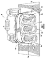
- FIGS. 1-2 another such power combiner 20 is shown.
- This wound-wire type toroidal power combiner 20 illustratively includes a circuit board 23, a 100-Ohm bridging resistor 24 installed on the circuit board for dissipating any power mismatch in input power supplies 31-32 (50-Ohm input impendence), and three toroidal transformers 25a-25c installed on the circuit board and defining a power combiner circuit.
- Each toroidal transformer 25a-25c illustratively includes a ferrite core 22a-22c and Teflon coated windings 21a-21c surrounding the respective ferrite core.
- the wound-wire type power combiner 20 illustratively includes a 50-Ohm load resistor 27 coupled to the toroidal transformer 25c .
- Teflon coated windings 21a-21c are typically hand wound through the ferrite cores 22a-22c and are used for their desirable high breakdown voltage properties. Moreover, Teflon coated windings may be costly. This makes the manufacturer of such HF power combiners time consuming and expensive.
- US 4,201,965 discloses a hi-Q inductor comprising a printed inductance.
- the printed inductance is obtained through four conductive traces structured as coils which are connected in series each other.
- the conductive coils are wound around sections of a ring-like electromagnetic core. The sections are inserted into opening 36 of the support of the printed inductance.
- RF radio frequency
- a printed circuit board according to claim 1 and having first and second opposing major surfaces, and a plurality of openings therethrough.
- the RF signal combiner/splitter also includes a ferromagnetic body comprising a first portion spaced from the first major surface of the PCB, a second portion spaced from the second major surface of the PCB, and a plurality of interconnecting portions coupling the first and second portions and extending through respective openings in the PCB.
- the PCB includes conductive traces cooperating with the ferromagnetic body to define circuitry, for example, operable over a frequency range of 2 to 30 MHz, for combining/splitting RF signals.
- the toroidal RF signal combiner/splitter may be manufactured without cumbersome wire windings.
- the circuitry for combining/splitting RF signals comprises a plurality of summing toroidal inductors.
- the PCB may further comprise additional conductive traces cooperating with the ferromagnetic body to define impedance matching circuitry coupled to the circuitry for combining/splitting RF signals.
- the impedance matching circuitry may comprise a plurality of transformer toroidal inductors.
- the RF signal combiner/splitter may further comprise a plurality of RF signal ports coupled to the conductive traces.
- the ferromagnetic body may also comprise a plurality of joined together segments.
- the RF signal combiner/splitter may further comprise at least one load resistor coupled to the conductive traces.
- the PCB may comprise at least one planar dielectric layer.
- Another aspect is directed to a method of making a circuit board PCB to operate as a radio frequency (RF) signal combiner/splitter defined in claim 6.
- the method includes providing a printed circuit board (PCB) having first and second opposing major surfaces, and a plurality of openings therethrough.
- the method also includes positioning a ferromagnetic body comprising a first portion spaced from the first major surface of the PCB, a second portion spaced from the second major surface of the PCB, and a plurality of interconnecting portions coupling the first and second portions and extending through respective openings in the PCB.
- the PCB comprises conductive traces cooperating with the ferromagnetic body to define circuitry for combining/splitting RF signals.
- the RF signal combiner/splitter 40 may be used as a combiner or a splitter depending on the direction of the signals.
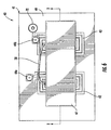
- the RF signal combiner/splitter 40 illustratively includes a printed circuit board (PCB) 41 .
- the PCB 41 has first 49 and second 51 opposing major surfaces and may include at least one planar dielectric layer and/or a ground plane.
- the PCB 41 also illustratively includes a plurality of openings 55a-55e therethrough.
- the openings 55a-55e are illustratively rectangle-shaped, but may have other shapes, for example, circular or N-sided polygonal shapes.
- the RF signal combiner/splitter 40 illustratively includes a ferromagnetic body 45 coupled through the PCB 41 .
- the ferromagnetic body 45 may comprise ferrite, for example, and illustratively includes a first portion 47 spaced from the first major surface 49 of the PCB 41 and a second portion 48 spaced from the second major surface 51 of the PCB.
- the ferromagnetic body 45 also illustratively includes a plurality of interconnecting portions 46a-46e coupling the first 47 and second 48 portions and extending through respective openings 55a-55e in the PCB 41 . Perhaps as best seen in FIGS. 4b and 5 , the ferromagnetic body 45 may also comprise a plurality of joined together segments 47-48.
- first 47 and second 48 portions of the ferromagnetic body 45 may be joined together with ferrite adhesive, for example.
- the ferromagnetic body may also comprise an integrally formed monolithic block, i.e. one piece.
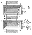
- the PCB 41 illustratively includes conductive traces 42-43 formed on the first major surface 49 .
- the conductive traces 42-43 may comprise copper or aluminum, for example.
- the conductive traces 42-43 cooperate with the ferromagnetic body 45 to define circuitry for combining/splitting RF signals.
- the RF signal combiner/splitter 40 illustratively includes a plurality of RF signal ports 44a-44b coupled to the conductive traces 42-43 .
- the circuitry of the RF signal combiner/splitter 40 illustratively includes a pair of radio frequency signal sources 54a-54b (50-Ohm input impendence) coupled to the RF signal ports 44a-44b , a 100-Ohm bridging resistor 70 coupled therebetween and for dissipating any power differential in the radio frequency signal sources, and a first set 52 of summing (combiner) toroidal inductors, i.e. coupled toroidal inductors, (2-three turn inductors), formed from the conductive traces and the ferromagnetic body, for combining the input power supplies.
- summing (combiner) toroidal inductors i.e. coupled toroidal inductors, (2-three turn inductors
- the circuitry of the RF signal combiner/splitter 40 also illustratively includes a second set 53 of transformer toroidal inductors (1-two turn inductor and 1-four turn inductor, i.e. 4T:6T auto transformer 1:2.25 Z(impedance)-ratio) for providing a step-up impedance transformer, and a 56.25 load impedance 73 also coupled to the conductive traces 42-43.
- the ideal load impedance would a 50-Ohm load; nonetheless, the illustrated embodiment includes a near ideal 56.25-Ohm load impedance 73.
- the RF signal combiner/splitter 40 illustratively includes a center tap wire 58 coupling the first set 52 of summing toroidal inductors to the second set 53 of transformer toroidal inductors.
- the center tap wire 58 may alternatively be formed on the first major surface 49 of the PCB 41 as a conductive trace.
- the circuitry of the RF signal combiner/splitter 40 is operable over a frequency range of, for example, 2 to 30 MHz for combining/splitting RF signals, i.e. high frequency signals.
- a chart 60 illustrates the electrical performance of the RF signal combiner/splitter 40 . More particularly, the left-side y-axis represents port loss in decibels and the x-axis represents frequency in MHz. The right-side y-axis represents port return loss in decibels.
- the RF signal combiner/splitter 40 is operated as a splitter, i.e. a single power source is fed into the output of the second set 53 of transformer toroidal inductors and two split signals are provided at the RF signal ports 44a-44b.
- the ideal splitter would receive input signal x(t) and output two split signals equaling 0.5*x(t), i.e. a power reduction of 3 decibels.
- Curves 61-62 demonstrate the near ideal performance (approximately -3 decibels) of the RF signal combiner/splitter 40 in the HF range, i.e. 2-30 MHz.
- Curves 63-64 demonstrate the near ideal return loss performance of the RF signal combiner/splitter 40 in the HF range, i.e. 2-30 MHz.
- the above described RF signal combiner/splitter 40 is toroidal and well suited for HF applications yet may be manufactured without cumbersome hand wound wire coils.
- the RF signal combiner/splitter 40 may be manufactured without intensive manual labor.
- the RF signal combiner/splitter 40 uses no soldering for assembly and may be manufactured before any wave soldering is used.
- the RF signal combiner/splitter 40 uses no external assemblies and is more mechanically robust than the typical wound-wire type power combiner.
- the RF signal combiner/splitter 40 is readily manufactured with repeatable and consistent performance since the manual manufacture component of the typical power combiner is removed.
- the RF signal combiner/splitter 40 does not use expensive Teflon coated windings, the cost of manufacture is reduced.
- Another aspect is directed to a method of making a circuit board PCB to operate as a RF signal combiner/splitter 40.
- the method includes providing a PCB 41 having first 49 and second 51 opposing major surfaces, and a plurality of openings 55a-55e therethrough.
- the method also includes positioning a ferromagnetic body 45 comprising a first portion 47 spaced from the first major surface 49 of the PCB 41, a second portion 48 spaced from the second major surface 51 of the PCB, and a plurality of interconnecting portions 46a-46e coupling the first and second portions and extending through respective openings 55a-55e in the PCB.
- the PCB 41 comprises conductive traces 42-43 cooperating with the ferromagnetic body 45 to define circuitry for combining/splitting RF signals.
Landscapes
- Engineering & Computer Science (AREA)
- Power Engineering (AREA)
- Multimedia (AREA)
- Microelectronics & Electronic Packaging (AREA)
- Chemical & Material Sciences (AREA)
- Composite Materials (AREA)
- Coils Or Transformers For Communication (AREA)
Claims (8)
- Carte de circuits imprimés PCB (41) ayant des première et deuxième surfaces principales (49, 51) opposées, et une pluralité d'ouvertures (55a-55c) à travers celles-ci ; et
un corps ferromagnétique (45) comprenant une première partie (47) espacée de la première surface principale (49) de ladite PCB (41), une deuxième partie (48) espacée de la deuxième surface principale (51) de ladite PCB (41), et une pluralité de parties d'interconnexion (46a-46e) couplant lesdites première et deuxième parties (47, 48) et s'étendant à travers des ouvertures (55a-55c) respectives dans ladite PCB (41) ;
ladite PCB (41) comprenant un premier et un deuxième tracé conducteur (42, 43) coopérant avec ledit corps ferromagnétique (45),
caractérisée en ce que le premier et le deuxième tracé conducteur (42, 43) coopèrent avec ledit corps ferromagnétique (45) pour définir un ensemble de circuits pour combiner/séparer des signaux RF, ledit ensemble de circuits comprenant une pluralité d'inducteurs (52) toroïdaux de sommation,
dans laquelle la pluralité de parties d'interconnexion (46a-46e) consiste en une première, une deuxième, une troisième, une quatrième et une cinquième partie d'interconnexion (46a-46e) consécutives et dans laquelle le premier et le deuxième tracé conducteur (42, 43) sont placés autour de la deuxième et de la quatrième partie d'interconnexion (46b, 46d). - Combineur/séparateur de signaux RF selon la revendication 1, dans lequel ladite PCB (41) comprend en outre des tracés conducteurs additionnels coopérant avec ledit corps ferromagnétique (45) pour définir un ensemble de circuits d'adaptation d'impédance couplé audit ensemble de circuits pour combiner/séparer des signaux RF.
- Combineur/séparateur de signaux RF selon la revendication 2, dans lequel ledit ensemble de circuits d'adaptation d'impédance comprend une pluralité d'inducteurs (53) toroïdaux de transformateur.
- Combineur/séparateur de signaux RF selon la revendication 1, comprenant en outre deux ports (44a, 44b) de signaux RF couplés auxdits premier et deuxième tracés conducteurs (42, 43).
- Combineur/séparateur de signaux RF selon la revendication 1 dans lequel ledit corps ferromagnétique (45) comprend une pluralité de segments (47, 48) joints ensemble.
- Procédé de fabrication d'une carte de circuits PCB (41) pour fonctionner comme un combineur/séparateur (40) de signaux en fréquence radio RF, comprenant :la prévision d'une carte de circuits imprimés PCB (41) ayant des première et deuxième surfaces principales (49, 51) opposées, et une pluralité d'ouvertures (55a-55c) à travers celles-ci ; etla mise en place d'un corps ferromagnétique (45) comprenant une première partie (47) espacée de la première surface principale (49) de la PCB (41), une deuxième partie (48) espacée de la deuxième surface principale (51) de la PCB (41), et une pluralité de parties d'interconnexion (46a-46e) couplant les première et deuxième parties (47, 48) et s'étendant à travers des ouvertures respectives dans la PCB (41) ;la PCB (41) comprenant un premier et un deuxième tracé conducteur (42, 43) coopérant avec le corps ferromagnétique (45) pour définir un ensemble de circuits pour combiner/séparer des signaux RF, ledit ensemble de circuits comprenant une pluralité d'inducteurs (52) toroïdaux de sommation,dans lequel la pluralité de parties d'interconnexion (46a-46e) consiste en une première, une deuxième, une troisième, une quatrième et une cinquième partie d'interconnexion (46a-46e) consécutives et dans lequel le premier et le deuxième tracé conducteur (42, 43) sont placés autour de la deuxième et de la quatrième partie d'interconnexion (46b, 46d).
- Procédé selon la revendication 6, comprenant en outre la prévision de la PCB (41) ayant des tracés conducteurs (43) additionnels coopérant avec le corps ferromagnétique (45) pour définir un ensemble de circuits d'adaptation d'impédance couplé à l'ensemble de circuits pour combiner/séparer des signaux RF.
- Procédé selon la revendication 6, comprenant en outre le couplage d'une pluralité de ports (44a, 44b) de signaux RF aux tracés conducteurs (42).
Applications Claiming Priority (2)
| Application Number | Priority Date | Filing Date | Title |
|---|---|---|---|
| US12/433,218 US8354894B2 (en) | 2009-04-30 | 2009-04-30 | RF signal combiner/splitter and related methods |
| PCT/US2010/032906 WO2010127073A1 (fr) | 2009-04-30 | 2010-04-29 | Combinateur/diviseur de signal rf et procédés associés |
Publications (2)
| Publication Number | Publication Date |
|---|---|
| EP2425690A1 EP2425690A1 (fr) | 2012-03-07 |
| EP2425690B1 true EP2425690B1 (fr) | 2014-07-16 |
Family
ID=42289463
Family Applications (1)
| Application Number | Title | Priority Date | Filing Date |
|---|---|---|---|
| EP10719162.9A Not-in-force EP2425690B1 (fr) | 2009-04-30 | 2010-04-29 | Combineur de signaux hf et rch statement et procédés associés |
Country Status (3)
| Country | Link |
|---|---|
| US (1) | US8354894B2 (fr) |
| EP (1) | EP2425690B1 (fr) |
| WO (1) | WO2010127073A1 (fr) |
Families Citing this family (10)
| Publication number | Priority date | Publication date | Assignee | Title |
|---|---|---|---|---|
| FR2938979B1 (fr) * | 2008-11-25 | 2010-12-31 | Thales Sa | Coupleur radiofrequence compact. |
| CN102291725B (zh) * | 2011-01-04 | 2014-09-10 | 京信通信系统(中国)有限公司 | 多模数字射频拉远系统 |
| US9251945B2 (en) * | 2013-04-09 | 2016-02-02 | Fred O. Barthold | Planar core with high magnetic volume utilization |
| CN107205666A (zh) | 2014-11-07 | 2017-09-26 | 伟伦公司 | 医疗设备 |
| US10157702B2 (en) * | 2014-12-07 | 2018-12-18 | Alpha And Omega Semiconductor (Cayman) Ltd. | Pulse transformer |
| CN107360142B (zh) * | 2017-06-26 | 2019-10-08 | 京信通信系统(中国)有限公司 | 基于cpri架构的多制式混合组网传输系统及传输方法 |
| US10554177B2 (en) | 2017-11-27 | 2020-02-04 | Skyworks Solutions, Inc. | Quadrature combined doherty amplifiers |
| WO2019103899A1 (fr) | 2017-11-27 | 2019-05-31 | Skyworks Solutions, Inc. | Combineur et diviseur de puissance à large bande |
| US10505700B1 (en) | 2018-07-12 | 2019-12-10 | T-Mobile Usa, Inc. | Reducing intermodulation distortion for intra-band dual connectivity |
| GB2623346A (en) * | 2022-10-13 | 2024-04-17 | Technetix Bv | Face plate for cable tap unit |
Family Cites Families (31)
| Publication number | Priority date | Publication date | Assignee | Title |
|---|---|---|---|---|
| US3428920A (en) * | 1966-11-29 | 1969-02-18 | Adams Russel Co Inc | N-way electrical power divider wherein n is an odd number |
| GB1440304A (en) * | 1974-11-29 | 1976-06-23 | Mullard Ltd | Transmission line pulse transformers |
| US4201965A (en) * | 1978-06-29 | 1980-05-06 | Rca Corporation | Inductance fabricated on a metal base printed circuit board |
| US4386324A (en) * | 1980-12-05 | 1983-05-31 | Hughes Aircraft Company | Planar chip-level power combiner |
| US4463326A (en) * | 1980-12-29 | 1984-07-31 | International Telephone And Telegraph Corporation | Planar N-way combiner/divider for microwave circuits |
| US4839616A (en) * | 1983-07-18 | 1989-06-13 | Harris Corporation | Broadband impedance transformer |
| US4647957A (en) * | 1983-10-11 | 1987-03-03 | At&T Bell Laboratories | Latchup-preventing CMOS device |
| DE3425153A1 (de) * | 1984-07-07 | 1986-01-16 | Robert Bosch Gmbh, 7000 Stuttgart | Elektrischer uebertrager |
| US4647868A (en) | 1985-03-25 | 1987-03-03 | General Electric Company | Push-pull radio-frequency power splitter/combiner apparatus |
| US5598327A (en) * | 1990-11-30 | 1997-01-28 | Burr-Brown Corporation | Planar transformer assembly including non-overlapping primary and secondary windings surrounding a common magnetic flux path area |
| GB2252208B (en) * | 1991-01-24 | 1995-05-03 | Burr Brown Corp | Hybrid integrated circuit planar transformer |
| US5334957A (en) | 1992-11-09 | 1994-08-02 | Harris Corporation | RF high power, two and three way in phase combiner and method |
| US5801602A (en) * | 1996-04-30 | 1998-09-01 | 3Com Corporation | Isolation and signal filter transformer |
| FI962803A0 (fi) * | 1996-07-10 | 1996-07-10 | Nokia Telecommunications Oy | Planartransformator |
| US5781093A (en) * | 1996-08-05 | 1998-07-14 | International Power Devices, Inc. | Planar transformer |
| US6529389B2 (en) * | 2000-04-06 | 2003-03-04 | Aria Corporation | Universal input miniature power supply with a single split transformer primary winding |
| US6420953B1 (en) * | 2000-05-19 | 2002-07-16 | Pulse Engineering. Inc. | Multi-layer, multi-functioning printed circuit board |
| US20040113739A1 (en) * | 2000-12-07 | 2004-06-17 | Delta Electronics Inc. | Low profile transformer |
| JP2002175922A (ja) * | 2000-12-08 | 2002-06-21 | Sansha Electric Mfg Co Ltd | 高周波大電流変圧器 |
| JP2002353032A (ja) * | 2001-05-18 | 2002-12-06 | Rotra Leiterplatten Produktions & Vertriebs Gmbh | 多層プリント板複合物とその製造のための方法 |
| US6888438B2 (en) * | 2001-06-15 | 2005-05-03 | City University Of Hong Kong | Planar printed circuit-board transformers with effective electromagnetic interference (EMI) shielding |
| DE10148133A1 (de) * | 2001-09-28 | 2003-04-24 | Ascom Energy Systems Ag Bern | Flachtransformator mit gesteckten Sekundärwicklungen |
| AU2002360464A1 (en) * | 2001-12-03 | 2003-06-17 | Memgen Corporation | Miniature rf and microwave components and methods for fabricating such components |
| US7239219B2 (en) | 2001-12-03 | 2007-07-03 | Microfabrica Inc. | Miniature RF and microwave components and methods for fabricating such components |
| US6750752B2 (en) * | 2002-11-05 | 2004-06-15 | Werlatone, Inc. | High power wideband balun and power combiner/divider incorporating such a balun |
| US7164903B1 (en) * | 2003-06-10 | 2007-01-16 | Smiths Interconnect Microwave Components, Inc. | Integrated N-way Wilkinson power divider/combiner |
| EP1699107B1 (fr) * | 2005-03-05 | 2017-05-31 | TRUMPF Hüttinger GmbH + Co. KG | Coupleur 3dB |
| GB0525799D0 (en) * | 2005-12-20 | 2006-01-25 | Rolls Royce Plc | Lightweight components |
| US7864013B2 (en) * | 2006-07-13 | 2011-01-04 | Double Density Magnetics Inc. | Devices and methods for redistributing magnetic flux density |
| JP4222490B2 (ja) * | 2006-09-29 | 2009-02-12 | Tdk株式会社 | プレーナ型トランス及びスイッチング電源 |
| US7872560B2 (en) * | 2007-03-19 | 2011-01-18 | Abc Taiwan Electronics Corp. | Independent planar transformer |
-
2009
- 2009-04-30 US US12/433,218 patent/US8354894B2/en active Active
-
2010
- 2010-04-29 EP EP10719162.9A patent/EP2425690B1/fr not_active Not-in-force
- 2010-04-29 WO PCT/US2010/032906 patent/WO2010127073A1/fr not_active Ceased
Also Published As
| Publication number | Publication date |
|---|---|
| US20100277253A1 (en) | 2010-11-04 |
| US8354894B2 (en) | 2013-01-15 |
| WO2010127073A1 (fr) | 2010-11-04 |
| EP2425690A1 (fr) | 2012-03-07 |
Similar Documents
| Publication | Publication Date | Title |
|---|---|---|
| US8354894B2 (en) | RF signal combiner/splitter and related methods | |
| Yeung | A compact dual-band 90° coupler with coupled-line sections | |
| JP4834551B2 (ja) | 平面結合器を一体成形したアンテナシステム | |
| US9298873B2 (en) | Method of designing impedance transformation circuit | |
| EP3853875B1 (fr) | Amplificateur de puissance rf avec transformateur symétrique-dissymétrique | |
| US9537198B2 (en) | Wideband impedance transformer | |
| Abbosh | Planar out-of-phase power divider/combiner for wideband high power microwave applications | |
| US6504464B2 (en) | Choke coil | |
| SG187775A1 (en) | Lcl high power combiner | |
| Liu et al. | A novel patterned ground structure with shunt and series lumped elements for synthesizing absorption common-mode filters | |
| US9614694B2 (en) | Wideband RF device | |
| US8077006B2 (en) | Transmission line impedance transformer and related methods | |
| US9362883B2 (en) | Passive radio frequency signal handler | |
| JP2643822B2 (ja) | バラントランス | |
| US20120040631A1 (en) | Compact Radiofrequency Coupler | |
| CN101233649A (zh) | 不可逆电路元件、复合电子零件及通信装置 | |
| US12519447B2 (en) | Electronic component and communication apparatus | |
| EP3155720B1 (fr) | Transformateur d'impédance à large bande | |
| KR101363251B1 (ko) | 광대역 전송선 발룬 트랜스포머 및 이를 이용한 전력 증폭기 | |
| Kang et al. | Differential transformer using bonder-wires and patterns on a printed circuit board for RF circuit applications | |
| JP2001006941A (ja) | 高周波トランスおよびインピーダンス変換器 | |
| JP4143950B2 (ja) | アイソレータ内蔵高周波複合回路 | |
| Heuermann | Passive RF Components Made from Concentrated Components | |
| Prajapati et al. | 2-Way UHF Compact Broadband High-Power Combiner/Divider with Unbalanced 50Ω Isolation Resistors | |
| WO2016136569A1 (fr) | Élément inductif, élément de transformateur à haute fréquence, élément de conversion d'impédance et dispositif d'antenne |
Legal Events
| Date | Code | Title | Description |
|---|---|---|---|
| PUAI | Public reference made under article 153(3) epc to a published international application that has entered the european phase |
Free format text: ORIGINAL CODE: 0009012 |
|
| 17P | Request for examination filed |
Effective date: 20111020 |
|
| AK | Designated contracting states |
Kind code of ref document: A1 Designated state(s): AT BE BG CH CY CZ DE DK EE ES FI FR GB GR HR HU IE IS IT LI LT LU LV MC MK MT NL NO PL PT RO SE SI SK SM TR |
|
| DAX | Request for extension of the european patent (deleted) | ||
| GRAP | Despatch of communication of intention to grant a patent |
Free format text: ORIGINAL CODE: EPIDOSNIGR1 |
|
| INTG | Intention to grant announced |
Effective date: 20130716 |
|
| GRAS | Grant fee paid |
Free format text: ORIGINAL CODE: EPIDOSNIGR3 |
|
| GRAP | Despatch of communication of intention to grant a patent |
Free format text: ORIGINAL CODE: EPIDOSNIGR1 |
|
| GRAS | Grant fee paid |
Free format text: ORIGINAL CODE: EPIDOSNIGR3 |
|
| GRAA | (expected) grant |
Free format text: ORIGINAL CODE: 0009210 |
|
| INTG | Intention to grant announced |
Effective date: 20140519 |
|
| AK | Designated contracting states |
Kind code of ref document: B1 Designated state(s): AT BE BG CH CY CZ DE DK EE ES FI FR GB GR HR HU IE IS IT LI LT LU LV MC MK MT NL NO PL PT RO SE SI SK SM TR |
|
| REG | Reference to a national code |
Ref country code: GB Ref legal event code: FG4D |
|
| REG | Reference to a national code |
Ref country code: CH Ref legal event code: EP |
|
| REG | Reference to a national code |
Ref country code: IE Ref legal event code: FG4D |
|
| REG | Reference to a national code |
Ref country code: AT Ref legal event code: REF Ref document number: 678291 Country of ref document: AT Kind code of ref document: T Effective date: 20140815 |
|
| REG | Reference to a national code |
Ref country code: DE Ref legal event code: R096 Ref document number: 602010017495 Country of ref document: DE Effective date: 20140828 |
|
| REG | Reference to a national code |
Ref country code: NL Ref legal event code: VDEP Effective date: 20140716 |
|
| REG | Reference to a national code |
Ref country code: AT Ref legal event code: MK05 Ref document number: 678291 Country of ref document: AT Kind code of ref document: T Effective date: 20140716 |
|
| REG | Reference to a national code |
Ref country code: LT Ref legal event code: MG4D |
|
| PG25 | Lapsed in a contracting state [announced via postgrant information from national office to epo] |
Ref country code: LT Free format text: LAPSE BECAUSE OF FAILURE TO SUBMIT A TRANSLATION OF THE DESCRIPTION OR TO PAY THE FEE WITHIN THE PRESCRIBED TIME-LIMIT Effective date: 20140716 Ref country code: ES Free format text: LAPSE BECAUSE OF FAILURE TO SUBMIT A TRANSLATION OF THE DESCRIPTION OR TO PAY THE FEE WITHIN THE PRESCRIBED TIME-LIMIT Effective date: 20140716 Ref country code: PT Free format text: LAPSE BECAUSE OF FAILURE TO SUBMIT A TRANSLATION OF THE DESCRIPTION OR TO PAY THE FEE WITHIN THE PRESCRIBED TIME-LIMIT Effective date: 20141117 Ref country code: FI Free format text: LAPSE BECAUSE OF FAILURE TO SUBMIT A TRANSLATION OF THE DESCRIPTION OR TO PAY THE FEE WITHIN THE PRESCRIBED TIME-LIMIT Effective date: 20140716 Ref country code: GR Free format text: LAPSE BECAUSE OF FAILURE TO SUBMIT A TRANSLATION OF THE DESCRIPTION OR TO PAY THE FEE WITHIN THE PRESCRIBED TIME-LIMIT Effective date: 20141017 Ref country code: BG Free format text: LAPSE BECAUSE OF FAILURE TO SUBMIT A TRANSLATION OF THE DESCRIPTION OR TO PAY THE FEE WITHIN THE PRESCRIBED TIME-LIMIT Effective date: 20141016 Ref country code: SE Free format text: LAPSE BECAUSE OF FAILURE TO SUBMIT A TRANSLATION OF THE DESCRIPTION OR TO PAY THE FEE WITHIN THE PRESCRIBED TIME-LIMIT Effective date: 20140716 Ref country code: NO Free format text: LAPSE BECAUSE OF FAILURE TO SUBMIT A TRANSLATION OF THE DESCRIPTION OR TO PAY THE FEE WITHIN THE PRESCRIBED TIME-LIMIT Effective date: 20141016 |
|
| PG25 | Lapsed in a contracting state [announced via postgrant information from national office to epo] |
Ref country code: AT Free format text: LAPSE BECAUSE OF FAILURE TO SUBMIT A TRANSLATION OF THE DESCRIPTION OR TO PAY THE FEE WITHIN THE PRESCRIBED TIME-LIMIT Effective date: 20140716 Ref country code: NL Free format text: LAPSE BECAUSE OF FAILURE TO SUBMIT A TRANSLATION OF THE DESCRIPTION OR TO PAY THE FEE WITHIN THE PRESCRIBED TIME-LIMIT Effective date: 20140716 Ref country code: IS Free format text: LAPSE BECAUSE OF FAILURE TO SUBMIT A TRANSLATION OF THE DESCRIPTION OR TO PAY THE FEE WITHIN THE PRESCRIBED TIME-LIMIT Effective date: 20141116 Ref country code: PL Free format text: LAPSE BECAUSE OF FAILURE TO SUBMIT A TRANSLATION OF THE DESCRIPTION OR TO PAY THE FEE WITHIN THE PRESCRIBED TIME-LIMIT Effective date: 20140716 Ref country code: LV Free format text: LAPSE BECAUSE OF FAILURE TO SUBMIT A TRANSLATION OF THE DESCRIPTION OR TO PAY THE FEE WITHIN THE PRESCRIBED TIME-LIMIT Effective date: 20140716 Ref country code: CY Free format text: LAPSE BECAUSE OF FAILURE TO SUBMIT A TRANSLATION OF THE DESCRIPTION OR TO PAY THE FEE WITHIN THE PRESCRIBED TIME-LIMIT Effective date: 20140716 |
|
| REG | Reference to a national code |
Ref country code: DE Ref legal event code: R097 Ref document number: 602010017495 Country of ref document: DE |
|
| PG25 | Lapsed in a contracting state [announced via postgrant information from national office to epo] |
Ref country code: SK Free format text: LAPSE BECAUSE OF FAILURE TO SUBMIT A TRANSLATION OF THE DESCRIPTION OR TO PAY THE FEE WITHIN THE PRESCRIBED TIME-LIMIT Effective date: 20140716 Ref country code: EE Free format text: LAPSE BECAUSE OF FAILURE TO SUBMIT A TRANSLATION OF THE DESCRIPTION OR TO PAY THE FEE WITHIN THE PRESCRIBED TIME-LIMIT Effective date: 20140716 Ref country code: CZ Free format text: LAPSE BECAUSE OF FAILURE TO SUBMIT A TRANSLATION OF THE DESCRIPTION OR TO PAY THE FEE WITHIN THE PRESCRIBED TIME-LIMIT Effective date: 20140716 Ref country code: DK Free format text: LAPSE BECAUSE OF FAILURE TO SUBMIT A TRANSLATION OF THE DESCRIPTION OR TO PAY THE FEE WITHIN THE PRESCRIBED TIME-LIMIT Effective date: 20140716 Ref country code: RO Free format text: LAPSE BECAUSE OF FAILURE TO SUBMIT A TRANSLATION OF THE DESCRIPTION OR TO PAY THE FEE WITHIN THE PRESCRIBED TIME-LIMIT Effective date: 20140716 |
|
| PLBE | No opposition filed within time limit |
Free format text: ORIGINAL CODE: 0009261 |
|
| STAA | Information on the status of an ep patent application or granted ep patent |
Free format text: STATUS: NO OPPOSITION FILED WITHIN TIME LIMIT |
|
| 26N | No opposition filed |
Effective date: 20150417 |
|
| PG25 | Lapsed in a contracting state [announced via postgrant information from national office to epo] |
Ref country code: SI Free format text: LAPSE BECAUSE OF FAILURE TO SUBMIT A TRANSLATION OF THE DESCRIPTION OR TO PAY THE FEE WITHIN THE PRESCRIBED TIME-LIMIT Effective date: 20140716 Ref country code: MC Free format text: LAPSE BECAUSE OF FAILURE TO SUBMIT A TRANSLATION OF THE DESCRIPTION OR TO PAY THE FEE WITHIN THE PRESCRIBED TIME-LIMIT Effective date: 20140716 Ref country code: LU Free format text: LAPSE BECAUSE OF FAILURE TO SUBMIT A TRANSLATION OF THE DESCRIPTION OR TO PAY THE FEE WITHIN THE PRESCRIBED TIME-LIMIT Effective date: 20150429 |
|
| REG | Reference to a national code |
Ref country code: CH Ref legal event code: PL |
|
| REG | Reference to a national code |
Ref country code: IE Ref legal event code: MM4A |
|
| PG25 | Lapsed in a contracting state [announced via postgrant information from national office to epo] |
Ref country code: CH Free format text: LAPSE BECAUSE OF NON-PAYMENT OF DUE FEES Effective date: 20150430 Ref country code: LI Free format text: LAPSE BECAUSE OF NON-PAYMENT OF DUE FEES Effective date: 20150430 |
|
| REG | Reference to a national code |
Ref country code: FR Ref legal event code: PLFP Year of fee payment: 7 |
|
| PG25 | Lapsed in a contracting state [announced via postgrant information from national office to epo] |
Ref country code: IE Free format text: LAPSE BECAUSE OF NON-PAYMENT OF DUE FEES Effective date: 20150429 |
|
| PG25 | Lapsed in a contracting state [announced via postgrant information from national office to epo] |
Ref country code: BE Free format text: LAPSE BECAUSE OF FAILURE TO SUBMIT A TRANSLATION OF THE DESCRIPTION OR TO PAY THE FEE WITHIN THE PRESCRIBED TIME-LIMIT Effective date: 20140716 |
|
| PGFP | Annual fee paid to national office [announced via postgrant information from national office to epo] |
Ref country code: DE Payment date: 20160427 Year of fee payment: 7 Ref country code: GB Payment date: 20160427 Year of fee payment: 7 |
|
| PGFP | Annual fee paid to national office [announced via postgrant information from national office to epo] |
Ref country code: IT Payment date: 20160421 Year of fee payment: 7 Ref country code: FR Payment date: 20160425 Year of fee payment: 7 |
|
| PG25 | Lapsed in a contracting state [announced via postgrant information from national office to epo] |
Ref country code: MT Free format text: LAPSE BECAUSE OF FAILURE TO SUBMIT A TRANSLATION OF THE DESCRIPTION OR TO PAY THE FEE WITHIN THE PRESCRIBED TIME-LIMIT Effective date: 20140716 |
|
| PG25 | Lapsed in a contracting state [announced via postgrant information from national office to epo] |
Ref country code: SM Free format text: LAPSE BECAUSE OF FAILURE TO SUBMIT A TRANSLATION OF THE DESCRIPTION OR TO PAY THE FEE WITHIN THE PRESCRIBED TIME-LIMIT Effective date: 20140716 Ref country code: HU Free format text: LAPSE BECAUSE OF FAILURE TO SUBMIT A TRANSLATION OF THE DESCRIPTION OR TO PAY THE FEE WITHIN THE PRESCRIBED TIME-LIMIT; INVALID AB INITIO Effective date: 20100429 |
|
| PG25 | Lapsed in a contracting state [announced via postgrant information from national office to epo] |
Ref country code: HR Free format text: LAPSE BECAUSE OF FAILURE TO SUBMIT A TRANSLATION OF THE DESCRIPTION OR TO PAY THE FEE WITHIN THE PRESCRIBED TIME-LIMIT Effective date: 20140716 |
|
| PG25 | Lapsed in a contracting state [announced via postgrant information from national office to epo] |
Ref country code: TR Free format text: LAPSE BECAUSE OF FAILURE TO SUBMIT A TRANSLATION OF THE DESCRIPTION OR TO PAY THE FEE WITHIN THE PRESCRIBED TIME-LIMIT Effective date: 20140716 |
|
| REG | Reference to a national code |
Ref country code: DE Ref legal event code: R119 Ref document number: 602010017495 Country of ref document: DE |
|
| GBPC | Gb: european patent ceased through non-payment of renewal fee |
Effective date: 20170429 |
|
| REG | Reference to a national code |
Ref country code: FR Ref legal event code: ST Effective date: 20171229 |
|
| PG25 | Lapsed in a contracting state [announced via postgrant information from national office to epo] |
Ref country code: FR Free format text: LAPSE BECAUSE OF NON-PAYMENT OF DUE FEES Effective date: 20170502 Ref country code: DE Free format text: LAPSE BECAUSE OF NON-PAYMENT OF DUE FEES Effective date: 20171103 |
|
| PG25 | Lapsed in a contracting state [announced via postgrant information from national office to epo] |
Ref country code: GB Free format text: LAPSE BECAUSE OF NON-PAYMENT OF DUE FEES Effective date: 20170429 |
|
| PG25 | Lapsed in a contracting state [announced via postgrant information from national office to epo] |
Ref country code: IT Free format text: LAPSE BECAUSE OF NON-PAYMENT OF DUE FEES Effective date: 20170429 |
|
| PG25 | Lapsed in a contracting state [announced via postgrant information from national office to epo] |
Ref country code: MK Free format text: LAPSE BECAUSE OF FAILURE TO SUBMIT A TRANSLATION OF THE DESCRIPTION OR TO PAY THE FEE WITHIN THE PRESCRIBED TIME-LIMIT Effective date: 20140716 |