EP2423989A2 - Coated reflective film for a light emitting device and method of manufacturing thereof - Google Patents
Coated reflective film for a light emitting device and method of manufacturing thereof Download PDFInfo
- Publication number
- EP2423989A2 EP2423989A2 EP11178646A EP11178646A EP2423989A2 EP 2423989 A2 EP2423989 A2 EP 2423989A2 EP 11178646 A EP11178646 A EP 11178646A EP 11178646 A EP11178646 A EP 11178646A EP 2423989 A2 EP2423989 A2 EP 2423989A2
- Authority
- EP
- European Patent Office
- Prior art keywords
- light emitting
- reflective film
- protective film
- emitting element
- electrically conductive
- Prior art date
- Legal status (The legal status is an assumption and is not a legal conclusion. Google has not performed a legal analysis and makes no representation as to the accuracy of the status listed.)
- Granted
Links
Images


Classifications
-
- H—ELECTRICITY
- H10—SEMICONDUCTOR DEVICES; ELECTRIC SOLID-STATE DEVICES NOT OTHERWISE PROVIDED FOR
- H10H—INORGANIC LIGHT-EMITTING SEMICONDUCTOR DEVICES HAVING POTENTIAL BARRIERS
- H10H20/00—Individual inorganic light-emitting semiconductor devices having potential barriers, e.g. light-emitting diodes [LED]
- H10H20/80—Constructional details
- H10H20/85—Packages
- H10H20/8506—Containers
-
- H—ELECTRICITY
- H10—SEMICONDUCTOR DEVICES; ELECTRIC SOLID-STATE DEVICES NOT OTHERWISE PROVIDED FOR
- H10H—INORGANIC LIGHT-EMITTING SEMICONDUCTOR DEVICES HAVING POTENTIAL BARRIERS
- H10H20/00—Individual inorganic light-emitting semiconductor devices having potential barriers, e.g. light-emitting diodes [LED]
- H10H20/80—Constructional details
- H10H20/81—Bodies
- H10H20/822—Materials of the light-emitting regions
- H10H20/824—Materials of the light-emitting regions comprising only Group III-V materials, e.g. GaP
- H10H20/825—Materials of the light-emitting regions comprising only Group III-V materials, e.g. GaP containing nitrogen, e.g. GaN
-
- H—ELECTRICITY
- H10—SEMICONDUCTOR DEVICES; ELECTRIC SOLID-STATE DEVICES NOT OTHERWISE PROVIDED FOR
- H10H—INORGANIC LIGHT-EMITTING SEMICONDUCTOR DEVICES HAVING POTENTIAL BARRIERS
- H10H20/00—Individual inorganic light-emitting semiconductor devices having potential barriers, e.g. light-emitting diodes [LED]
- H10H20/80—Constructional details
- H10H20/83—Electrodes
- H10H20/831—Electrodes characterised by their shape
-
- H—ELECTRICITY
- H10—SEMICONDUCTOR DEVICES; ELECTRIC SOLID-STATE DEVICES NOT OTHERWISE PROVIDED FOR
- H10H—INORGANIC LIGHT-EMITTING SEMICONDUCTOR DEVICES HAVING POTENTIAL BARRIERS
- H10H20/00—Individual inorganic light-emitting semiconductor devices having potential barriers, e.g. light-emitting diodes [LED]
- H10H20/80—Constructional details
- H10H20/84—Coatings, e.g. passivation layers or antireflective coatings
-
- H—ELECTRICITY
- H10—SEMICONDUCTOR DEVICES; ELECTRIC SOLID-STATE DEVICES NOT OTHERWISE PROVIDED FOR
- H10H—INORGANIC LIGHT-EMITTING SEMICONDUCTOR DEVICES HAVING POTENTIAL BARRIERS
- H10H20/00—Individual inorganic light-emitting semiconductor devices having potential barriers, e.g. light-emitting diodes [LED]
- H10H20/80—Constructional details
- H10H20/85—Packages
-
- H—ELECTRICITY
- H10—SEMICONDUCTOR DEVICES; ELECTRIC SOLID-STATE DEVICES NOT OTHERWISE PROVIDED FOR
- H10H—INORGANIC LIGHT-EMITTING SEMICONDUCTOR DEVICES HAVING POTENTIAL BARRIERS
- H10H20/00—Individual inorganic light-emitting semiconductor devices having potential barriers, e.g. light-emitting diodes [LED]
- H10H20/80—Constructional details
- H10H20/85—Packages
- H10H20/851—Wavelength conversion means
- H10H20/8511—Wavelength conversion means characterised by their material, e.g. binder
- H10H20/8512—Wavelength conversion materials
-
- H—ELECTRICITY
- H10—SEMICONDUCTOR DEVICES; ELECTRIC SOLID-STATE DEVICES NOT OTHERWISE PROVIDED FOR
- H10H—INORGANIC LIGHT-EMITTING SEMICONDUCTOR DEVICES HAVING POTENTIAL BARRIERS
- H10H20/00—Individual inorganic light-emitting semiconductor devices having potential barriers, e.g. light-emitting diodes [LED]
- H10H20/80—Constructional details
- H10H20/85—Packages
- H10H20/855—Optical field-shaping means, e.g. lenses
- H10H20/856—Reflecting means
-
- H—ELECTRICITY
- H10—SEMICONDUCTOR DEVICES; ELECTRIC SOLID-STATE DEVICES NOT OTHERWISE PROVIDED FOR
- H10H—INORGANIC LIGHT-EMITTING SEMICONDUCTOR DEVICES HAVING POTENTIAL BARRIERS
- H10H20/00—Individual inorganic light-emitting semiconductor devices having potential barriers, e.g. light-emitting diodes [LED]
- H10H20/80—Constructional details
- H10H20/85—Packages
- H10H20/857—Interconnections, e.g. lead-frames, bond wires or solder balls
-
- H—ELECTRICITY
- H10—SEMICONDUCTOR DEVICES; ELECTRIC SOLID-STATE DEVICES NOT OTHERWISE PROVIDED FOR
- H10W—GENERIC PACKAGES, INTERCONNECTIONS, CONNECTORS OR OTHER CONSTRUCTIONAL DETAILS OF DEVICES COVERED BY CLASS H10
- H10W72/00—Interconnections or connectors in packages
- H10W72/01—Manufacture or treatment
- H10W72/015—Manufacture or treatment of bond wires
- H10W72/01515—Forming coatings
-
- H—ELECTRICITY
- H10—SEMICONDUCTOR DEVICES; ELECTRIC SOLID-STATE DEVICES NOT OTHERWISE PROVIDED FOR
- H10W—GENERIC PACKAGES, INTERCONNECTIONS, CONNECTORS OR OTHER CONSTRUCTIONAL DETAILS OF DEVICES COVERED BY CLASS H10
- H10W72/00—Interconnections or connectors in packages
- H10W72/071—Connecting or disconnecting
- H10W72/075—Connecting or disconnecting of bond wires
-
- H—ELECTRICITY
- H10—SEMICONDUCTOR DEVICES; ELECTRIC SOLID-STATE DEVICES NOT OTHERWISE PROVIDED FOR
- H10W—GENERIC PACKAGES, INTERCONNECTIONS, CONNECTORS OR OTHER CONSTRUCTIONAL DETAILS OF DEVICES COVERED BY CLASS H10
- H10W74/00—Encapsulations, e.g. protective coatings
-
- H—ELECTRICITY
- H10—SEMICONDUCTOR DEVICES; ELECTRIC SOLID-STATE DEVICES NOT OTHERWISE PROVIDED FOR
- H10W—GENERIC PACKAGES, INTERCONNECTIONS, CONNECTORS OR OTHER CONSTRUCTIONAL DETAILS OF DEVICES COVERED BY CLASS H10
- H10W90/00—Package configurations
- H10W90/701—Package configurations characterised by the relative positions of pads or connectors relative to package parts
- H10W90/751—Package configurations characterised by the relative positions of pads or connectors relative to package parts of bond wires
- H10W90/756—Package configurations characterised by the relative positions of pads or connectors relative to package parts of bond wires between a chip and a stacked lead frame, conducting package substrate or heat sink
Definitions
- the present invention relates to a method of manufacturing a light emitting device having a light emitting element disposed on an electrically conductive member.
- an object of the present invention is to provide a light emitting device capable of maintaining high optical output power while suppressing discoloration of the reflective film and a method of manufacturing thereof.
- a method of manufacturing a light emitting device includes, in an order of, an electrically conductive member preparation step of preparing an electrically conductive member provided with a reflective film, a light emitting element disposing step of disposing a light emitting element on the reflective film, and a protective film forming step of forming a protective film on the reflective film by using an atomic layer deposition method.
- a method of manufacturing a light emitting device includes, in an order of, an electrically conductive member preparation step of preparing an electrically conductive member, a light emitting element disposing step of disposing a light emitting element on the reflective film, a wiring step of electrically connecting the electrically conductive member and the light emitting element by using a wire, a reflective film forming step of forming a reflective film on each surface of the electrically conductive member and wire, and a protective film forming step of forming a protective film on the reflective film by using an atomic layer deposition method.
- a light emitting device includes, an electrically conductive member provided with a reflective film; a light emitting element mounted on the reflective film; and a protective film continuously covering a surface of the light emitting element and a surface of the reflective film, wherein a thickness of the protective film on the reflective film in a vicinity of the light emitting element is substantially equal to a thickness of the protective film on the reflective film in the region except for the vicinity of the light emitting element.
- a light emitting device capable of maintaining high optical output power while suppressing discoloration of the reflective film and a method of manufacturing thereof may be obtained.
- the preferred embodiments are intended as illustrative of a method of manufacturing a light emitting device to give a concrete form to technical ideas of the present invention, and the scope of the invention is not limited to those described below.
- the sizes, materials, shapes and the relative positions of the members described in examples are given as an example and not as a limitation to the scope of the invention unless specifically stated.
- the sizes and the positional relationships of the members in each of the drawings are occasionally shown exaggerated for ease of explanation.
- an electrically conductive member 1 having a reflective film 1b provided on a base member la is prepared (electrically conductive member preparation step).
- the electrically conductive member is constituted with a base member and a reflective film.
- the material of the base member la is not specifically limited as long as it has electric conductivity.
- the base member 1a for example, copper or a copper alloy can be used.
- the material of the reflective film 1b is not specifically limited as long as it is capable of reflecting light from the light emitting element 3.
- the reflective film 1b for example, silver, aluminum or the like can be used, and particularly, a material containing silver, which has high reflectance is preferably used.
- the base member la and the reflective film 1b are not separately illustrated but are collectively illustrated as the electrically conductive member 1, for the simplicity of explanation.
- the electrically conductive member may be made solely of a reflective film, or may have another member interposing between the base member 1a and the reflective film 1b.
- the reflective film 1b is not needed to be disposed on the entire upper surface of the base member la, as long as the reflective film 1b is disposed in the region in the vicinity of the light emitting element 3 (region A in FIG. 2 ).
- a package 2 having a base portion 2a and a side wall 2b respectively provided on an electrically conductive member 1 may be formed (package forming step.
- the material of the package is not specifically limited and, for example, a resin or a ceramic may be used.
- an electrically conductive member 1 is arranged in a mold for package (not shown) and a resin for the package is introduced into the mold and is harden, thus, the package 2 and the electrically conductive member 1 can be integrally formed. A part of the electrically conductive member 1 is exposed on the bottom surface of a recess defined in the package.
- the package 2 is formed integrally with the electrically conductive member 1, and the material thereof is not specifically limited as long as the material is electrically insulating.
- a material of the package 2 an electrically insulating material having excellent light resistance and heat resistance is suitably used, and for example, a thermoplastic resin such as a polyphthalamide, a thermosetting resin such as an epoxy resin, and a glass epoxy and a ceramics can be use.
- a structure of the package 2 having a side wall 2b is employed, but the side wall is not necessarily to be provided.
- a light emitting element 3 is disposed on the reflective film 1b (light emitting element disposing step). More specifically, the light emitting element 3 can be disposed on the reflective film 1b with interposing an adhesive member (not shown) therebetween.
- the adhesive member may either be electrically conductive or electrically insulating.
- the adhesive member is for arranging and fixing the light emitting element 3 on the electrically conductive member 1 and the material thereof is not specifically limited.
- an electrically insulating adhesive member an epoxy resin or a silicone resin can be employed and in the case where an electrically conductive adhesive member to be used, an Au-Sn alloy, a SnAgCu alloy, a SnPb alloy, an InSn alloy, Ag, Sn, or Ag can be employed.
- a known light emitting element can be used and, for example, an LED made of a nitride semiconductor (In X Al Y Ga 1-X-Y N, 0 ⁇ X, 0 ⁇ Y, X+Y ⁇ 1) capable of emitting blue light or green light can be used.
- a nitride semiconductor In X Al Y Ga 1-X-Y N, 0 ⁇ X, 0 ⁇ Y, X+Y ⁇ 1
- the light emitting element 3 and the reflective film 1b can be electrically connected by using an electrically conductive wire 4 (wiring step).
- the light emitting element 3 and the base member la are electrically connected through the electrically conductive reflective film 1b.
- the light emitting element 3 has a pair of electrodes (not shown) on the same surface side, and the light emitting element 3 is disposed with the side which has the electrodes facing upward (emission observing surface side), a wire 4 is needed to connect with each electrode as shown in the figure.
- the adhesive member does not need to be electrically insulating and an electrically conductive member such as a metal can be used in view of thermal conductivity.
- an electrode is provided on each of the opposite surfaces with respect to the light emitting element, electric current is supplied to one of the electrodes through an electrically conductive adhesive member, so that only one wire is needed.
- the light emitting element has a pair of electrodes on the same surface side and is disposed with that side down (opposite side from the emission observing surface (the opposite side from the electrically conductive member 1)), the electric current can be supplied to each of the electrode through the respective electrically conductive adhesive members, so that a wire is not needed.
- the wire 4 is used for electrically connecting the light emitting element 3 with the base member 1a, and the material thereof is not specifically limited.
- the material of the wire 4 for example, a material containing at least one of gold, copper, platinum, aluminum, and silver can be used.
- ALD atomic layer deposition
- TMA trimethyl aluminum
- H 2 O water
- TMA gas is introduced to react with the hydroxyl group on the surface of the reflective film which is the object (first reaction).
- the excess gas is purged.
- H 2 O gas is introduced to react with the TMA which is bonded to the hydroxyl group in the first reaction (second reaction).
- the excess gas is purged.
- setting the first reaction, purging, the second reaction, and purging as one cycle the cycle is repeated to obtain Al 2 O 3 with a predetermined thickness.
- a reaction constituent travels in a less straight line in ALD. Therefore, the reaction component can be supplied even to a portion in the vicinity of an obstacle, so that a single molecular layer of the reaction component can be deposited at each time, even to a portion in the vicinity of an obstacle. As a result, a protective film of higher quality can be deposited with more uniform thickness and film quality even to a region in the vicinity of an obstacle, as well as to other regions free of obstacles.
- Protective film obtained by using ALD has higher quality and higher protective property compared to that of the protective films obtained by using a conventional method.
- partial discoloration occurs with a certain proportion even in a region free from an obstacle in a protective film obtained by using a conventional method, however, a protective film obtained by using ALD exhibits substantially no discoloration regardless of the presence of an obstacle.
- the protective film obtained by using ADL is capable of sufficiently protecting the reflective film.
- the protective film can be provided with a smaller thickness than that of the protective films obtained by using a conventional method. With this arrangement, the absorption of light by the protective film can be suppressed and a light emitting device having high optical output power in its initial properties can be obtained.
- the protective film 5 is formed after disposing the light emitting element 3, when a conventional method is used, there has been a problem that the light emitting element 3 itself acts as an obstacle, preventing the material constituent of the protective film 5 from sufficiently reaching the portions at or near the periphery of the light emitting element 3.
- the resulting reduction in quality and/or insufficient thickness of the protective film 5 has caused deterioration and discoloration of the reflective film in a region in the vicinity of the light emitting element 3 (region A in FIG. 2 ) - This is considered that a larger number of pin holes compared with that in the other portions occur in the deteriorated portions of the protective film, causing sulfurization or bromination of the reflective film which leads occurrence of discoloration.
- the portions in the vicinity of the light emitting element can produce high optical output power, so that if discoloration of the reflective film in the vicinity of the light emitting element occurs, the optical output power of the light emitting device will be significantly decreased.
- the protective film 5 with excellent film quality and the like can be obtained even in the region (region A in FIG. 2 ) in the vicinity of the light emitting element. As a result, occurrence of discoloration or the like in the reflective film 1b of the region A can be suppressed. Further, with employing ADL, a thickness of the protective film 5 on the reflective film 1b in the vicinity of the light emitting element is substantially equal to a thickness of the protective film 5 on the reflective film 1b in the region except for the vicinity of the light emitting element in addition to forming the protective film 5 with excellent film quality.
- the protective film 5 with excellent film quality can be formed, with a thickness required to prevent discoloration of the reflective film 1b even in the vicinity of the light emitting element that would be an obstacle when forming the protective film 5, which makes it possible to effectively prevent deterioration of the reflective film 1b.
- a gap may be created between the circumference of the bottom surface of the light emitting element and the reflective film.
- the protective film can be formed also on the reflective film in the gap.
- the protective film is to be formed using a conventional method after the wiring step, there has been a problem that the existence of wire 4 (the wire 4 acts as an obstacle) prevents the material constituent of the protective film 5 from sufficiently reaching the reflective film 1b beneath the wire 4.
- the resulting reduction in quality and/or insufficient thickness of the protective film 5 has caused discoloration of the reflective film 1b in the portion.
- the regions beneath the wire 4 there has been a problem in the region in the vicinity of the connecting portion of the wire 4 and the reflective film 1b (region B in FIG. 2 ) that when a conventional method is used, not only discoloration of the reflective film 1a but also corrosion of the reflective film 1b takes place and results in breaking of the wire 4.
- the protective film 5 with excellent film quality and the like can be formed even in the region (region B in FIG. 2 ) directly under the wire 4. Accordingly, deterioration of the protective film in the region B can be reduced and not only discoloration but also braking of the wire can be suppressed.
- the protective film 5 is formed so as to fill a gap formed between an edge portion of the wire 4 connected to the reflective film 1b and the reflective film 1b, thereby preventing discoloration and corrosion of the reflective film 1b positioned around the gap.
- the protective film 5 is formed on the reflective film 1b around the edge portion of the wire 4 with a substantially equal thickness.
- a thickness of the protective film 5 on the reflective film 1b in the vicinity of the edge portion of the wire 4 is substantially equal to a thickness of the protective film 5 on the reflective film 1b in the region except for the vicinity of the edge portion of the wire 4. Therefore, discoloration and corrosion of the reflective film 1b around the edge portion of the wire 4 can be effectively prevented.
- FIGS. 4A and 4B each shows the image around the connecting portion of the wire and the reflective film, taken from the emission observing surface side after the protective film depositing step.
- FIG. 4A shows a protective film made of Al 2 O 3 with a thickness of 30 nm, deposited by using ALD
- FIG. 4B shows a protective film made of Al 2 O 3 with a thickness of 30 nm, deposited by using a conventional sputtering method.
- the protective film formed by using ALD showed no discoloration not only in the regions away from the wire and free of obstacles but also in the region (corresponding to region B in FIG. 2 ) directly under the wire.
- the protective film formed by using ALD showed no discoloration not only in the regions away from the wire and free of obstacles but also in the region (corresponding to region B in FIG. 2 ) directly under the wire.
- the protective film deposited by sputtering showed dot shaped discoloration at a number of positions even in the regions away from the wire and free of obstacles, and showed continuous discoloration in the regions around the connecting portion of the wire and the reflective film, including the region directly under the wire (this is considered that microscopic unevenness exists in the connecting portion of the wire and the reflective film and acts as an obstacle, so that discoloration occurred not only in the region directly under the wire but also in the entire region around the connecting portion) .
- the results of the experiments described above exhibit that forming the protective film with a use of ALD enables to obtain a protective film of excellent quality.
- a wire made of a material containing silver which has high reflectance can be employed to obtain efficient light reflection from the wire.
- discoloration of the wire which is made of a silver-containing material may also present a problem.
- the protective film can be formed on the entire surface of the wire including the emission observing surface side of the wire to the opposite side (reflective film side) of the wire, with the reason as described above. Thus, discoloration or the like of the wire can be suppressed efficiently.
- the protective film is formed with a use of a conventional method after the package forming step, there has been a problem that due to the existence of the side wall of the package 2 (the side wall of the package acts as an obstacle), the material constituent of the protective film 5 cannot sufficiently reach a portion of the bottom surface defining the recess in the vicinity of the side wall (region C in FIG. 2 ).
- the resulting reduction in quality and/or insufficient thickness of the protective film 5 caused discoloration of corresponding part of the reflective film 1b.
- Discoloration of the protective film 1b in the vicinity of the side wall of the package 2 may not pose harmful effect on the optical output power as that of the discoloration of the reflective film 1b in the region A, but the problem can never be ignored.
- the protective film 5 which is excellent in film quality and the like can be obtained even in the region (region C in FIG. 2 ) in the vicinity of the side wall 2b.
- occurrence of discoloration of the protective film 1b in the region C can be suppressed and decrease in the optical output power of the light emitting device can be further reduced.
- the protective film 1b contains silver
- the optical output power tends to decrease due to discoloration, of the reflective film 1b in the course of time.
- the protective film formed by using ALD is capable of efficiently suppressing occurrence of discoloration or the like, even in a case where the protective film is made of a silver-containing material, and thus is preferable.
- the protective film 5 for example, aluminum oxide (Al 2 O 3 ), silicon dioxide (SiO 2 ), aluminum nitride (AlN), or silicon nitride (Si 3 N 4 ) can be employed, and preferably, aluminum oxide or silicone dioxide, more preferably aluminum oxide can be used. With this arrangement, absorption of light from the light emitting element can be suppressed and a protective film of excellent protection property can be obtained.
- Al 2 O 3 silicon dioxide
- AlN aluminum nitride
- Si 3 N 4 silicon nitride
- the thickness of the protective film 5 can be 1 nm or greater and less than 50 nm, preferably 2 nm or greater and less than 25 nm, more preferably 3 nm or greater and less than 10 nm.
- the protective film 5 is formed not only on the bottom surface defining the recess of the package 2 but also on the upper surface and inner wall of the side wall 2b, but for example, the upper surface and inner wall of the side wall 2b can be arranged so that the protective film 5 is not formed thereon.
- a region which is free of the protective film 5 can be provided in a part of the bottom surface defining the recess of the package 2.
- a sealing member 6 can be formed in the recess defined by the side wall 2b of the package (sealing member forming step). Then, after cutting the electrically conductive member 1 so as to obtain each light emitting device capable of functioning individually (electrically conductive member cutting step), if required, each electrically conductive member 1 is bent to the back side of the corresponding package 2 (electrically conductive member bending step), to form individual light emitting devices.
- the sealing member 6 is to enclose the light emitting element 3, and the material thereof is not specifically limited as long as it allows the light from the light emitting element 3 to pass through to the outside.
- the material of the sealing member 6 for example, a silicone resin, an epoxy resin, or the like can be used.
- a fluorescent substance capable of emitting light upon receiving the light from the light emitting element 3 can be included also in the sealing member 6.
- a known substance can be used, and in the case where the light emitting element 3 emits blue light, a yellow light emitting fluorescent substance such as a YAG-based fluorescent substance, a TAG-based fluorescent substance, and a strontium silicate-based fluorescent substance can be used to obtain white light emission from the light emitting device.
- the electrically conductive member 1 is prepared (electrically conductive member preparation step).
- the electrically conductive member is made of the base member alone, and the reflective film 1b is not provided in this step.
- a package 2 having a base portion 2a and a side wall 2b provided on an electrically conductive member 1 can be formed (Package Forming Step).
- a light emitting element 3 is disposed on the electrically conductive member 1 (light emitting element disposing step). More specifically, the light emitting element 3 can be disposed on the electrically conductive member 1 using an adhesive member (not shown).
- the electrically conductive member 1 and the light emitting element 3 are electrically connected by using an electrically conductive wire 4 (wiring step).
- the reflective film 1b is formed on the surface of the electrically conductive member 1 and the wire 4 (reflective film forming step).
- the reflective film 1b on the surface of each wire 4 is not shown in FIG. 3E , but according to the present embodiment, the reflective film 1b is actually formed not only on the surface of each electrically conductive member 1 but also on the surface of each wire 4.
- the reflective film 1b also covers the connecting portion of the electrically conductive member 1 and the wire 4.
- the reflective film 1b For the method of forming the reflective film 1b, a known method can be employed. Particularly, with a use of an electroplating method, the reflective film 1b can be formed selectively on the surfaces of the electrically conductive member 1, the wire 4, or the like, without forming the reflective film (metal film) on the surface of the light emitting element 3 which is not electrically conductive.
- the material of the reflective film 1b the same materials as in the first embodiment can be used, and silver or the like can be employed.
- the protective film 5 is formed on the surface of the reflective film 1b by using ALD.
- the protective film 5 on the surface of each wire 4 is not shown in FIG. 3F , but in the present embodiment, actually, the protective film 5 is formed also on the surface of each wire 4 over the reflective film 1b.
- a sealing member 6 can be formed in the recess defined by the side wall 2b of the package (sealing member forming step). Then, after cutting the electrically conductive member 1 so as to obtain each light emitting device capable of functioning individually (electrically conductive member cutting step), if required, each electrically conductive member 1 is bent to the back side of the corresponding package 2 (electrically conductive member bending step), to form individual light emitting devices.
- the method of manufacturing the light emitting device according to the present invention can be applied to manufacturing various kinds of light emitting devices such as illumination light sources, light sources for various kinds of indicators, light sources for automobile use, light sources for displays, back light sources for liquid crystal displays, light sources for sensors, signals, and so on.
- various other embodiments and variants may occur to those skilled in the art, which are within the scope and spirit of the invention, and such other embodiments and variants are intended to be covered by the following claims.
- This application is based on applications No. 2010-187806 filed in Japan on Aug. 25, 2010, and No. 2010-203920 filed in Japan on Sep. 13, 2010, the contents of which are incorporated hereinto by references.
Landscapes
- Led Device Packages (AREA)
Abstract
Description
- The present invention relates to a method of manufacturing a light emitting device having a light emitting element disposed on an electrically conductive member.
- Attempts have been made in a light emitting device using a light emitting element as a light source to improve optical output power by disposing a reflective film containing silver and the like around the light emitting element, and further to suppress discoloration or the like of a reflective film by forming a protective film made of an inorganic material by way of sputtering, CVD or the like (see for example, Patent reference 1:
JP 2009-224538A - However, when a conventional method is used, there has been a problem that although the optical output power can be improved by the reflective film, decrease in optical output power occurs during the operation. That is, in the case of sputtering, CVD, or the like, a material constituent travels more or less in a straight line toward the object and is deposited thereon to form a protective film. Therefore, for example, in the vicinity of a light emitting element, the light emitting element itself becomes an obstacle and thus a protective film of good quality has been unable to be obtained. As a result, deterioration of the reflective film starts to take place from such a portion and which causes discoloration of the reflective film.
- Accordingly, an object of the present invention is to provide a light emitting device capable of maintaining high optical output power while suppressing discoloration of the reflective film and a method of manufacturing thereof.
- A method of manufacturing a light emitting device according to an aspect of the present invention includes, in an order of, an electrically conductive member preparation step of preparing an electrically conductive member provided with a reflective film, a light emitting element disposing step of disposing a light emitting element on the reflective film, and a protective film forming step of forming a protective film on the reflective film by using an atomic layer deposition method.
- A method of manufacturing a light emitting device according to another aspect of the present invention includes, in an order of, an electrically conductive member preparation step of preparing an electrically conductive member, a light emitting element disposing step of disposing a light emitting element on the reflective film, a wiring step of electrically connecting the electrically conductive member and the light emitting element by using a wire, a reflective film forming step of forming a reflective film on each surface of the electrically conductive member and wire, and a protective film forming step of forming a protective film on the reflective film by using an atomic layer deposition method.
- A light emitting device according to an aspect of the present invention includes, an electrically conductive member provided with a reflective film; a light emitting element mounted on the reflective film; and a protective film continuously covering a surface of the light emitting element and a surface of the reflective film, wherein a thickness of the protective film on the reflective film in a vicinity of the light emitting element is substantially equal to a thickness of the protective film on the reflective film in the region except for the vicinity of the light emitting element.
- According to the present invention, a light emitting device capable of maintaining high optical output power while suppressing discoloration of the reflective film and a method of manufacturing thereof may be obtained.
Preferred embodiments of the present invention will be described below with reference to the accompanying drawings. -
-
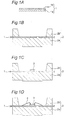
FIGS. 1A trough 1F are schematic diagrams for illustrating a method of manufacturing a light emitting device according to an embodiment of the present invention. -
FIG.2 is a magnified schematic view of the portion encircled with dashed line inFIG. 1F . -
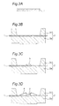
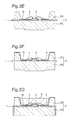
FIGS. 3A trough 3G are schematic diagrams for illustrating a method of manufacturing a light emitting device according to another embodiment of the present invention. -
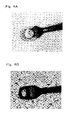
FIG. 4A is a photograph around the connecting portion of the wire and the reflective film covered with the protective film deposited by using ALD. -
FIG. 4B is a photograph around the connecting portion of the wire and the reflective film covered with the protective film deposited by using a conventional sputtering method. -
FIG. 5A is a magnified section view of an edge portion of the wire connected to the reflective film in an embodiment of the present invention. -
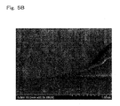
FIG. 5B is a photograph corresponding toFig.5A . - The preferred embodiments are intended as illustrative of a method of manufacturing a light emitting device to give a concrete form to technical ideas of the present invention, and the scope of the invention is not limited to those described below. Particularly, the sizes, materials, shapes and the relative positions of the members described in examples are given as an example and not as a limitation to the scope of the invention unless specifically stated. The sizes and the positional relationships of the members in each of the drawings are occasionally shown exaggerated for ease of explanation.
-
-
FIGS. 1A through 1F show each step of a method of manufacturing a light emitting device according to the present embodiment. -
FIG. 2 is a magnified schematic view of the portion encircled with dashed line inFIG. 1F . - First, as shown in
FIG. 1A , an electricallyconductive member 1 having areflective film 1b provided on a base member la is prepared (electrically conductive member preparation step). In this embodiment, not only thebase member 1a but also thereflective film 1b also has an electric conductivity. In the present embodiment, the electrically conductive member is constituted with a base member and a reflective film. - The material of the base member la is not specifically limited as long as it has electric conductivity. For the
base member 1a, for example, copper or a copper alloy can be used. - The material of the
reflective film 1b is not specifically limited as long as it is capable of reflecting light from thelight emitting element 3. For thereflective film 1b, for example, silver, aluminum or the like can be used, and particularly, a material containing silver, which has high reflectance is preferably used. - In
FIGS 1B to 1F , the base member la and thereflective film 1b are not separately illustrated but are collectively illustrated as the electricallyconductive member 1, for the simplicity of explanation. The electrically conductive member may be made solely of a reflective film, or may have another member interposing between thebase member 1a and thereflective film 1b. Further, thereflective film 1b is not needed to be disposed on the entire upper surface of the base member la, as long as thereflective film 1b is disposed in the region in the vicinity of the light emitting element 3 (region A inFIG. 2 ). - Next, as shown in
FIG. 1B , for example, apackage 2 having abase portion 2a and aside wall 2b respectively provided on an electricallyconductive member 1 may be formed (package forming step. - The material of the package is not specifically limited and, for example, a resin or a ceramic may be used. In the case where the package is made of a resin, an electrically
conductive member 1 is arranged in a mold for package (not shown) and a resin for the package is introduced into the mold and is harden, thus, thepackage 2 and the electricallyconductive member 1 can be integrally formed. A part of the electricallyconductive member 1 is exposed on the bottom surface of a recess defined in the package. - The
package 2 is formed integrally with the electricallyconductive member 1, and the material thereof is not specifically limited as long as the material is electrically insulating. As a material of thepackage 2, an electrically insulating material having excellent light resistance and heat resistance is suitably used, and for example, a thermoplastic resin such as a polyphthalamide, a thermosetting resin such as an epoxy resin, and a glass epoxy and a ceramics can be use. In the present embodiment, a structure of thepackage 2 having aside wall 2b is employed, but the side wall is not necessarily to be provided. - Next, as shown in
FIG. 1C , alight emitting element 3 is disposed on thereflective film 1b (light emitting element disposing step). More specifically, thelight emitting element 3 can be disposed on thereflective film 1b with interposing an adhesive member (not shown) therebetween. The adhesive member may either be electrically conductive or electrically insulating. - The adhesive member is for arranging and fixing the
light emitting element 3 on the electricallyconductive member 1 and the material thereof is not specifically limited. For example, in the case where an electrically insulating adhesive member is to be used, an epoxy resin or a silicone resin can be employed and in the case where an electrically conductive adhesive member to be used, an Au-Sn alloy, a SnAgCu alloy, a SnPb alloy, an InSn alloy, Ag, Sn, or Ag can be employed. - For the
light emitting element 3, a known light emitting element can be used and, for example, an LED made of a nitride semiconductor (InXAlYGa1-X-YN, 0≤X, 0≤Y, X+Y≤1) capable of emitting blue light or green light can be used. - Next, as shown in
FIG. 1D , thelight emitting element 3 and thereflective film 1b can be electrically connected by using an electrically conductive wire 4 (wiring step). In this arrangement, thelight emitting element 3 and the base member la are electrically connected through the electrically conductivereflective film 1b. - In the case where the
light emitting element 3 has a pair of electrodes (not shown) on the same surface side, and thelight emitting element 3 is disposed with the side which has the electrodes facing upward (emission observing surface side), awire 4 is needed to connect with each electrode as shown in the figure. In this case, if the electrically conductive member side of thelight emitting element 3 has electrically insulating property, the adhesive member does not need to be electrically insulating and an electrically conductive member such as a metal can be used in view of thermal conductivity. In the case where an electrode is provided on each of the opposite surfaces with respect to the light emitting element, electric current is supplied to one of the electrodes through an electrically conductive adhesive member, so that only one wire is needed. On the other hand, in the case where the light emitting element has a pair of electrodes on the same surface side and is disposed with that side down (opposite side from the emission observing surface (the opposite side from the electrically conductive member 1)), the electric current can be supplied to each of the electrode through the respective electrically conductive adhesive members, so that a wire is not needed. - The
wire 4 is used for electrically connecting thelight emitting element 3 with thebase member 1a, and the material thereof is not specifically limited. For the material of thewire 4, for example, a material containing at least one of gold, copper, platinum, aluminum, and silver can be used. - Next, as shown in
FIG. 1E , using an atomic layer deposition method (hereinafter may be referred to as "ALD" (Atomic Layer Deposition), aprotective film 5 is deposited and formed on thereflective film 1b. That is, theprotective film 5 is deposited from the emission observing surface side. Different from a conventional method such as sputtering, ALD is a method for depositing a layer of reaction constituent as a single-atom layer at each time. The following describes a case where a protective film of aluminum oxide Al2O3) is deposited and formed using TMA (trimethyl aluminum) and water (H2O). - First, TMA gas is introduced to react with the hydroxyl group on the surface of the reflective film which is the object (first reaction). Next, the excess gas is purged. Thereafter, H2O gas is introduced to react with the TMA which is bonded to the hydroxyl group in the first reaction (second reaction). Next, the excess gas is purged. Then, setting the first reaction, purging, the second reaction, and purging as one cycle, the cycle is repeated to obtain Al2O3 with a predetermined thickness.
- Unlike that in the case of sputtering, CVD, or the like, a reaction constituent travels in a less straight line in ALD. Therefore, the reaction component can be supplied even to a portion in the vicinity of an obstacle, so that a single molecular layer of the reaction component can be deposited at each time, even to a portion in the vicinity of an obstacle. As a result, a protective film of higher quality can be deposited with more uniform thickness and film quality even to a region in the vicinity of an obstacle, as well as to other regions free of obstacles.
- Protective film obtained by using ALD has higher quality and higher protective property compared to that of the protective films obtained by using a conventional method. Thus, partial discoloration occurs with a certain proportion even in a region free from an obstacle in a protective film obtained by using a conventional method, however, a protective film obtained by using ALD exhibits substantially no discoloration regardless of the presence of an obstacle. Further, even with a small thickness, the protective film obtained by using ADL is capable of sufficiently protecting the reflective film. Thus, the protective film can be provided with a smaller thickness than that of the protective films obtained by using a conventional method. With this arrangement, the absorption of light by the protective film can be suppressed and a light emitting device having high optical output power in its initial properties can be obtained.
- In the case where the
protective film 5 is formed after disposing thelight emitting element 3, when a conventional method is used, there has been a problem that thelight emitting element 3 itself acts as an obstacle, preventing the material constituent of theprotective film 5 from sufficiently reaching the portions at or near the periphery of thelight emitting element 3. The resulting reduction in quality and/or insufficient thickness of theprotective film 5 has caused deterioration and discoloration of the reflective film in a region in the vicinity of the light emitting element 3 (region A inFIG. 2 ) - This is considered that a larger number of pin holes compared with that in the other portions occur in the deteriorated portions of the protective film, causing sulfurization or bromination of the reflective film which leads occurrence of discoloration. The portions in the vicinity of the light emitting element can produce high optical output power, so that if discoloration of the reflective film in the vicinity of the light emitting element occurs, the optical output power of the light emitting device will be significantly decreased. - Accordingly, with employing ADL, the
protective film 5 with excellent film quality and the like can be obtained even in the region (region A inFIG. 2 ) in the vicinity of the light emitting element. As a result, occurrence of discoloration or the like in thereflective film 1b of the region A can be suppressed. Further, with employing ADL, a thickness of theprotective film 5 on thereflective film 1b in the vicinity of the light emitting element is substantially equal to a thickness of theprotective film 5 on thereflective film 1b in the region except for the vicinity of the light emitting element in addition to forming theprotective film 5 with excellent film quality. Therefore, according to the method of the present invention, theprotective film 5 with excellent film quality can be formed, with a thickness required to prevent discoloration of thereflective film 1b even in the vicinity of the light emitting element that would be an obstacle when forming theprotective film 5, which makes it possible to effectively prevent deterioration of thereflective film 1b. - Particularly, in the case where the adhesive member presents within the circumference of the light emitting element and without reaching a side surface of the light emitting element when seen in a cross-sectional view, a gap may be created between the circumference of the bottom surface of the light emitting element and the reflective film. Even in such a case, with using ALD, the protective film can be formed also on the reflective film in the gap.
- In the case where the protective film is to be formed using a conventional method after the wiring step, there has been a problem that the existence of wire 4 (the
wire 4 acts as an obstacle) prevents the material constituent of theprotective film 5 from sufficiently reaching thereflective film 1b beneath thewire 4. The resulting reduction in quality and/or insufficient thickness of theprotective film 5 has caused discoloration of thereflective film 1b in the portion. Particularly, among the regions beneath thewire 4, there has been a problem in the region in the vicinity of the connecting portion of thewire 4 and thereflective film 1b (region B inFIG. 2 ) that when a conventional method is used, not only discoloration of thereflective film 1a but also corrosion of thereflective film 1b takes place and results in breaking of thewire 4. - However, with a use of ADL, the
protective film 5 with excellent film quality and the like can be formed even in the region (region B inFIG. 2 ) directly under thewire 4. Accordingly, deterioration of the protective film in the region B can be reduced and not only discoloration but also braking of the wire can be suppressed. - In addition, according to the method of manufacturing in which the
protective film 5 is formed by means of ALD, theprotective film 5 is formed so as to fill a gap formed between an edge portion of thewire 4 connected to thereflective film 1b and thereflective film 1b, thereby preventing discoloration and corrosion of thereflective film 1b positioned around the gap. - In addition, according to the present invention, in spite of a form of the
wire 4, for example, a shape of the edge portion of thewire 4 and a direction of thewire 4 extending from the edge portion etc., theprotective film 5 is formed on thereflective film 1b around the edge portion of thewire 4 with a substantially equal thickness. - Further, according to the present invention, a thickness of the
protective film 5 on thereflective film 1b in the vicinity of the edge portion of thewire 4 is substantially equal to a thickness of theprotective film 5 on thereflective film 1b in the region except for the vicinity of the edge portion of thewire 4. Therefore, discoloration and corrosion of thereflective film 1b around the edge portion of thewire 4 can be effectively prevented. -
FIGS. 4A and 4B each shows the image around the connecting portion of the wire and the reflective film, taken from the emission observing surface side after the protective film depositing step.FIG. 4A shows a protective film made of Al2O3 with a thickness of 30 nm, deposited by using ALD, andFIG. 4B shows a protective film made of Al2O3 with a thickness of 30 nm, deposited by using a conventional sputtering method. These images were taken after the reflective films made of Ag were left in a condition of excess sulfide for a given period time to facilitate sulfurization of the films (both were tested under the same condition). As shown inFIG. 4A , even exposed under an easily-sulfurized condition, the protective film formed by using ALD showed no discoloration not only in the regions away from the wire and free of obstacles but also in the region (corresponding to region B inFIG. 2 ) directly under the wire. On the other hand, as shown inFIG. 4B , the protective film deposited by sputtering showed dot shaped discoloration at a number of positions even in the regions away from the wire and free of obstacles, and showed continuous discoloration in the regions around the connecting portion of the wire and the reflective film, including the region directly under the wire (this is considered that microscopic unevenness exists in the connecting portion of the wire and the reflective film and acts as an obstacle, so that discoloration occurred not only in the region directly under the wire but also in the entire region around the connecting portion) . The results of the experiments described above exhibit that forming the protective film with a use of ALD enables to obtain a protective film of excellent quality. - In order to improve the optical output power of the light emitting device, for example, a wire made of a material containing silver which has high reflectance can be employed to obtain efficient light reflection from the wire. However, as in the case of discoloration of reflective film, discoloration of the wire which is made of a silver-containing material may also present a problem. Even in such a case, with a use of ALD, the protective film can be formed on the entire surface of the wire including the emission observing surface side of the wire to the opposite side (reflective film side) of the wire, with the reason as described above. Thus, discoloration or the like of the wire can be suppressed efficiently.
- In the case where the protective film is formed with a use of a conventional method after the package forming step, there has been a problem that due to the existence of the side wall of the package 2 (the side wall of the package acts as an obstacle), the material constituent of the
protective film 5 cannot sufficiently reach a portion of the bottom surface defining the recess in the vicinity of the side wall (region C inFIG. 2 ). The resulting reduction in quality and/or insufficient thickness of theprotective film 5 caused discoloration of corresponding part of thereflective film 1b. Discoloration of theprotective film 1b in the vicinity of the side wall of thepackage 2 may not pose harmful effect on the optical output power as that of the discoloration of thereflective film 1b in the region A, but the problem can never be ignored. - Accordingly, with employing ADL, the
protective film 5 which is excellent in film quality and the like can be obtained even in the region (region C inFIG. 2 ) in the vicinity of theside wall 2b. With this arrangement, occurrence of discoloration of theprotective film 1b in the region C can be suppressed and decrease in the optical output power of the light emitting device can be further reduced. - In the case where the
protective film 1b contains silver, there has been a problem that although having high reflectance is an advantageous property, with a use of a conventional method, the optical output power tends to decrease due to discoloration, of thereflective film 1b in the course of time. However, the protective film formed by using ALD is capable of efficiently suppressing occurrence of discoloration or the like, even in a case where the protective film is made of a silver-containing material, and thus is preferable. - For the
protective film 5, for example, aluminum oxide (Al2O3), silicon dioxide (SiO2), aluminum nitride (AlN), or silicon nitride (Si3N4) can be employed, and preferably, aluminum oxide or silicone dioxide, more preferably aluminum oxide can be used. With this arrangement, absorption of light from the light emitting element can be suppressed and a protective film of excellent protection property can be obtained. - The thickness of the
protective film 5 can be 1 nm or greater and less than 50 nm, preferably 2 nm or greater and less than 25 nm, more preferably 3 nm or greater and less than 10 nm. With this arrangement, while maintaining the functions as a protective film, absorption of light from the light emitting element by the protective film can be suppressed, so that the light emitting element of high optical output power can be obtained. - As shown in the figures such as
FIG. 1E , theprotective film 5 is formed not only on the bottom surface defining the recess of thepackage 2 but also on the upper surface and inner wall of theside wall 2b, but for example, the upper surface and inner wall of theside wall 2b can be arranged so that theprotective film 5 is not formed thereon. A region which is free of theprotective film 5 can be provided in a part of the bottom surface defining the recess of thepackage 2. - As shown in
FIG. 1F , if required, a sealingmember 6 can be formed in the recess defined by theside wall 2b of the package (sealing member forming step). Then, after cutting the electricallyconductive member 1 so as to obtain each light emitting device capable of functioning individually (electrically conductive member cutting step), if required, each electricallyconductive member 1 is bent to the back side of the corresponding package 2 (electrically conductive member bending step), to form individual light emitting devices. - The sealing
member 6 is to enclose thelight emitting element 3, and the material thereof is not specifically limited as long as it allows the light from thelight emitting element 3 to pass through to the outside. For the material of the sealingmember 6, for example, a silicone resin, an epoxy resin, or the like can be used. Further, a fluorescent substance capable of emitting light upon receiving the light from thelight emitting element 3 can be included also in the sealingmember 6. For the fluorescent substance, a known substance can be used, and in the case where thelight emitting element 3 emits blue light, a yellow light emitting fluorescent substance such as a YAG-based fluorescent substance, a TAG-based fluorescent substance, and a strontium silicate-based fluorescent substance can be used to obtain white light emission from the light emitting device. - SECOND EMBODIMENT The present embodiment will be described below with reference to
FIGS. 3A to 3G . In this embodiment, like members as in the first embodiment are designated by like numerals and their repeated description will be omitted. - First, as shown in
FIG. 3A , the electricallyconductive member 1 is prepared (electrically conductive member preparation step). In the present embodiment, different from that in the first embodiment, the electrically conductive member is made of the base member alone, and thereflective film 1b is not provided in this step. - Next, as shown in
FIG. 3B , apackage 2 having abase portion 2a and aside wall 2b provided on an electricallyconductive member 1 can be formed (Package Forming Step). - Next, as shown in
FIG. 3C , alight emitting element 3 is disposed on the electrically conductive member 1 (light emitting element disposing step). More specifically, thelight emitting element 3 can be disposed on the electricallyconductive member 1 using an adhesive member (not shown). - Next, as shown in
FIG. 3D , the electricallyconductive member 1 and thelight emitting element 3 are electrically connected by using an electrically conductive wire 4 (wiring step). - Next, the
reflective film 1b is formed on the surface of the electricallyconductive member 1 and the wire 4 (reflective film forming step). For the sake of drawing the figure, thereflective film 1b on the surface of eachwire 4 is not shown inFIG. 3E , but according to the present embodiment, thereflective film 1b is actually formed not only on the surface of each electricallyconductive member 1 but also on the surface of eachwire 4. Thereflective film 1b also covers the connecting portion of the electricallyconductive member 1 and thewire 4. - With this arrangement, absorption of light by the surface of the
wires 4 can be suppressed and a light emitting device of further higher optical output power can be obtained. - For the method of forming the
reflective film 1b, a known method can be employed. Particularly, with a use of an electroplating method, thereflective film 1b can be formed selectively on the surfaces of the electricallyconductive member 1, thewire 4, or the like, without forming the reflective film (metal film) on the surface of thelight emitting element 3 which is not electrically conductive. For the material of thereflective film 1b, the same materials as in the first embodiment can be used, and silver or the like can be employed. - Next, as shown in
FIG. 3F , theprotective film 5 is formed on the surface of thereflective film 1b by using ALD. For the sake of drawing the figure, theprotective film 5 on the surface of eachwire 4 is not shown inFIG. 3F , but in the present embodiment, actually, theprotective film 5 is formed also on the surface of eachwire 4 over thereflective film 1b. - As shown in
FIG. 3G , if required, a sealingmember 6 can be formed in the recess defined by theside wall 2b of the package (sealing member forming step). Then, after cutting the electricallyconductive member 1 so as to obtain each light emitting device capable of functioning individually (electrically conductive member cutting step), if required, each electricallyconductive member 1 is bent to the back side of the corresponding package 2 (electrically conductive member bending step), to form individual light emitting devices. - The method of manufacturing the light emitting device according to the present invention can be applied to manufacturing various kinds of light emitting devices such as illumination light sources, light sources for various kinds of indicators, light sources for automobile use, light sources for displays, back light sources for liquid crystal displays, light sources for sensors, signals, and so on.
It is to be understood that although the present invention has been described with regard to preferred embodiments thereof, various other embodiments and variants may occur to those skilled in the art, which are within the scope and spirit of the invention, and such other embodiments and variants are intended to be covered by the following claims.
This application is based on applications No.2010-187806 2010-203920
Claims (11)
- A method of manufacturing a light emitting device comprising steps of:preparing an electrically conductive member provided with a reflective film;disposing a light emitting element on the reflective film; andforming a protective film on the reflective film by means of an atomic layer deposition method.
- The method of manufacturing a light emitting device according to claim 1, further comprising a step of electrically connecting the reflective film and the light emitting element by a wire between the step of disposing a light emitting element and the step of forming a protective film.
- The method of manufacturing a light emitting device according to claims 1 or 2, further comprising a step of forming a package having a side wall on the electrically conductive member between the step of preparing an electrically conductive member and the step of disposing a light emitting element.
- A method of manufacturing a light emitting device comprising steps of:preparing an electrically conductive member;disposing a light emitting element on the electrically conductive member;connecting a wire to electrically connect the electrically conductive member and the light emitting element;forming a reflective film on a surface of the electrically conductive member and wire; andforming a protective film on the reflective film by means of an atomic layer deposition method.
- The method of manufacturing a light emitting device according to one of claims 1 to 4, wherein the reflective film contains silver.
- The method of manufacturing a light emitting device according to one of claims 1 to 5, wherein the protective film is made of aluminum oxide or silicon dioxide.
- The method of manufacturing a light emitting device according to claim 4, wherein in the step of forming a reflective film, the reflective film is formed by means of an electroplating method.
- A light emitting device comprising:an electrically conductive member provided with a reflective film;a light emitting element mounted on the reflective film; anda protective film continuously covering a surface of the light emitting element and a surface of the reflective filmwherein a thickness of the protective film on the reflective film in a vicinity of the light emitting element is substantially equal to a thickness of the protective film on the reflective film in the region except for the vicinity of the light emitting element.
- The light emitting device according to claim 8,
wherein the light emitting element is connected to the reflective film with a wire, and wherein
the protective film is formed so as to fill a gap formed between an edge portion of the wire connected to the reflective film and the reflective film. - The light emitting device according to claim 9,
wherein the protective film is formed on the reflective film around the edge portion of the wire with a substantially equal thickness. - The light emitting device according to claim 9 or 10,
wherein a thickness of the protective film on the reflective film in a vicinity of the edge portion of the wire is substantially equal to a thickness of the protective film on the reflective film in a region except for the vicinity of the edge portion of the wire.
Applications Claiming Priority (2)
| Application Number | Priority Date | Filing Date | Title |
|---|---|---|---|
| JP2010187806 | 2010-08-25 | ||
| JP2010203920A JP5864089B2 (en) | 2010-08-25 | 2010-09-13 | Method for manufacturing light emitting device |
Publications (3)
| Publication Number | Publication Date |
|---|---|
| EP2423989A2 true EP2423989A2 (en) | 2012-02-29 |
| EP2423989A3 EP2423989A3 (en) | 2014-08-06 |
| EP2423989B1 EP2423989B1 (en) | 2019-03-27 |
Family
ID=44719291
Family Applications (1)
| Application Number | Title | Priority Date | Filing Date |
|---|---|---|---|
| EP11178646.3A Active EP2423989B1 (en) | 2010-08-25 | 2011-08-24 | Coated reflective film for a light emitting device and method of manufacturing thereof |
Country Status (6)
| Country | Link |
|---|---|
| US (3) | US8679871B2 (en) |
| EP (1) | EP2423989B1 (en) |
| JP (1) | JP5864089B2 (en) |
| KR (1) | KR101844603B1 (en) |
| CN (2) | CN102386288B (en) |
| TW (1) | TWI616000B (en) |
Cited By (2)
| Publication number | Priority date | Publication date | Assignee | Title |
|---|---|---|---|---|
| EP2793278A3 (en) * | 2013-04-18 | 2015-10-28 | Nichia Corporation | Package for a light emitting device, and light emitting device including the same |
| WO2018188976A1 (en) * | 2017-04-12 | 2018-10-18 | Osram Opto Semiconductors Gmbh | Optoelectronic component |
Families Citing this family (35)
| Publication number | Priority date | Publication date | Assignee | Title |
|---|---|---|---|---|
| DE102009058796A1 (en) | 2009-12-18 | 2011-06-22 | OSRAM Opto Semiconductors GmbH, 93055 | Optoelectronic component and method for producing an optoelectronic component |
| JP6007897B2 (en) | 2011-04-11 | 2016-10-19 | 日亜化学工業株式会社 | Semiconductor light emitting device and manufacturing method thereof |
| JP6203478B2 (en) * | 2012-06-06 | 2017-09-27 | 日立化成株式会社 | OPTICAL SEMICONDUCTOR DEVICE, MANUFACTURING METHOD THEREOF, SUBSTRATE USED FOR MANUFACTURING |
| JP6203479B2 (en) * | 2012-06-06 | 2017-09-27 | 日立化成株式会社 | OPTICAL SEMICONDUCTOR DEVICE, MANUFACTURING METHOD THEREOF, SUBSTRATE USED FOR MANUFACTURING |
| JP5975269B2 (en) * | 2012-06-07 | 2016-08-23 | 日亜化学工業株式会社 | Method for manufacturing light emitting device |
| JP6102696B2 (en) | 2012-12-11 | 2017-03-29 | 日亜化学工業株式会社 | LIGHT EMITTING DEVICE AND METHOD FOR PRODUCING OPTICAL COMPONENT USED FOR THE SAME |
| DE102013100818B4 (en) * | 2013-01-28 | 2023-07-27 | OSRAM Opto Semiconductors Gesellschaft mit beschränkter Haftung | Optoelectronic semiconductor chip and method for producing an optoelectronic semiconductor chip |
| JP6145626B2 (en) * | 2013-05-01 | 2017-06-14 | 株式会社昭和真空 | Deposition method |
| JP6221387B2 (en) | 2013-06-18 | 2017-11-01 | 日亜化学工業株式会社 | Light emitting device and manufacturing method thereof |
| JP6232792B2 (en) * | 2013-07-17 | 2017-11-22 | 日亜化学工業株式会社 | Light emitting device |
| CN103441203B (en) * | 2013-07-24 | 2017-01-18 | 重庆四联光电科技有限公司 | Packaging method and packaging structure for semiconductor device |
| US11041118B2 (en) | 2013-08-29 | 2021-06-22 | Nichia Corporation | Fluoride fluorescent material and method for producing the same as well as light emitting device using the same |
| JP6255872B2 (en) * | 2013-10-08 | 2018-01-10 | 日亜化学工業株式会社 | Light emitting device and manufacturing method thereof |
| JP6237174B2 (en) * | 2013-12-05 | 2017-11-29 | 日亜化学工業株式会社 | Light emitting device |
| JP6277388B2 (en) * | 2014-01-14 | 2018-02-14 | 株式会社昭和真空 | Deposition method |
| US9755116B2 (en) | 2014-03-14 | 2017-09-05 | Nichia Corporation | Method of manufacturing light emitting device |
| JP6187509B2 (en) * | 2014-03-14 | 2017-08-30 | 日亜化学工業株式会社 | Light emitting device and manufacturing method thereof |
| JP6398323B2 (en) | 2014-05-25 | 2018-10-03 | 日亜化学工業株式会社 | Manufacturing method of semiconductor light emitting device |
| US9455300B1 (en) * | 2015-03-02 | 2016-09-27 | Rayvio Corporation | Pixel array of ultraviolet light emitting devices |
| JP6507007B2 (en) * | 2015-03-27 | 2019-04-24 | 東レエンジニアリング株式会社 | LED module and method of manufacturing LED module |
| JP6176287B2 (en) | 2015-06-10 | 2017-08-09 | 日亜化学工業株式会社 | Light emitting device and manufacturing method thereof |
| JP6327232B2 (en) | 2015-10-30 | 2018-05-23 | 日亜化学工業株式会社 | LIGHT EMITTING DEVICE AND LIGHT EMITTING MODULE MANUFACTURING METHOD |
| US10424699B2 (en) | 2016-02-26 | 2019-09-24 | Nichia Corporation | Light emitting device |
| US10347806B2 (en) * | 2017-04-12 | 2019-07-09 | Luminus, Inc. | Packaged UV-LED device with anodic bonded silica lens and no UV-degradable adhesive |
| WO2019079021A1 (en) * | 2017-10-19 | 2019-04-25 | Lumileds Llc | Light emitting device package |
| US10672960B2 (en) * | 2017-10-19 | 2020-06-02 | Lumileds Llc | Light emitting device package with a coating layer |
| JP6428894B2 (en) * | 2017-11-01 | 2018-11-28 | 日亜化学工業株式会社 | Light emitting device |
| TWI648878B (en) * | 2018-05-15 | 2019-01-21 | 東貝光電科技股份有限公司 | LED light source, LED light source manufacturing method and direct type display thereof |
| JP6601550B2 (en) * | 2018-10-31 | 2019-11-06 | 日亜化学工業株式会社 | Light emitting device |
| CN110797332A (en) * | 2019-11-07 | 2020-02-14 | 苏州晶台光电有限公司 | Method for improving moisture resistance of SMD LED package |
| CN111326644A (en) * | 2020-04-02 | 2020-06-23 | 盐城东山精密制造有限公司 | A kind of LED device and its packaging method |
| JP7387978B2 (en) | 2021-04-20 | 2023-11-29 | 日亜化学工業株式会社 | light emitting device |
| EP4160704B1 (en) * | 2021-09-29 | 2024-12-18 | Nichia Corporation | Light emitting device and method of manufacturing light emitting device |
| JP7401809B2 (en) * | 2021-09-29 | 2023-12-20 | 日亜化学工業株式会社 | Light-emitting device and method for manufacturing the light-emitting device |
| KR20240136788A (en) * | 2023-03-07 | 2024-09-19 | 삼성전자주식회사 | Light emitting device package and lighting device including the same |
Citations (3)
| Publication number | Priority date | Publication date | Assignee | Title |
|---|---|---|---|---|
| JP2009224538A (en) | 2008-03-17 | 2009-10-01 | Citizen Holdings Co Ltd | Semiconductor light emitting device |
| JP2010187806A (en) | 2009-02-17 | 2010-09-02 | Olympia:Kk | Pachinko game machine |
| JP2010203920A (en) | 2009-03-03 | 2010-09-16 | Nec Corp | Aircraft control system |
Family Cites Families (26)
| Publication number | Priority date | Publication date | Assignee | Title |
|---|---|---|---|---|
| JPS6285481A (en) | 1985-10-09 | 1987-04-18 | Nippon Telegr & Teleph Corp <Ntt> | Resin-sealed light emitting diode and manufacture thereof |
| JPH0353858U (en) | 1989-09-29 | 1991-05-24 | ||
| JPH114020A (en) * | 1997-04-15 | 1999-01-06 | Toshiba Corp | Semiconductor light emitting element, method of manufacturing the same, and semiconductor light emitting device |
| WO2000079605A1 (en) * | 1999-06-23 | 2000-12-28 | Citizen Electronics Co., Ltd. | Light emitting diode |
| CN1323441C (en) * | 2001-10-12 | 2007-06-27 | 日亚化学工业株式会社 | Light emitting device and manufacturing method thereof |
| JP2004193280A (en) | 2002-12-10 | 2004-07-08 | Fujitsu Ltd | Semiconductor device and manufacturing method thereof |
| US7331691B2 (en) * | 2004-10-29 | 2008-02-19 | Goldeneye, Inc. | Light emitting diode light source with heat transfer means |
| JP2007109915A (en) | 2005-10-14 | 2007-04-26 | Stanley Electric Co Ltd | Light emitting diode |
| FI121341B (en) | 2006-02-02 | 2010-10-15 | Beneq Oy | Silver protective coating |
| JP5233087B2 (en) * | 2006-06-28 | 2013-07-10 | 日亜化学工業株式会社 | LIGHT EMITTING DEVICE AND ITS MANUFACTURING METHOD, PACKAGE, LIGHT EMITTING DEVICE MOUNTING BOARD |
| JP4858032B2 (en) | 2006-09-15 | 2012-01-18 | 日亜化学工業株式会社 | Light emitting device |
| US7767589B2 (en) | 2007-02-07 | 2010-08-03 | Raytheon Company | Passivation layer for a circuit device and method of manufacture |
| JP5087304B2 (en) | 2007-03-30 | 2012-12-05 | 富士フイルム株式会社 | Manufacturing method of solid-state imaging device |
| JP5630948B2 (en) | 2007-07-04 | 2014-11-26 | 日亜化学工業株式会社 | Light emitting device |
| US7967476B2 (en) * | 2007-07-04 | 2011-06-28 | Nichia Corporation | Light emitting device including protective glass film |
| US7956469B2 (en) | 2007-07-27 | 2011-06-07 | Nichia Corporation | Light emitting device and method of manufacturing the same |
| JP5245594B2 (en) * | 2007-07-27 | 2013-07-24 | 日亜化学工業株式会社 | Light emitting device and manufacturing method thereof |
| JP4962270B2 (en) * | 2007-10-31 | 2012-06-27 | 日亜化学工業株式会社 | Light emitting device and method of manufacturing the same |
| JP4167717B1 (en) * | 2007-11-21 | 2008-10-22 | E&E Japan株式会社 | Light emitting device and manufacturing method thereof |
| US20110008550A1 (en) | 2008-01-25 | 2011-01-13 | Mitsui Engineering & Shipbuilding Co., Ltd | Atomic layer growing apparatus and thin film forming method |
| JP5195084B2 (en) | 2008-06-30 | 2013-05-08 | Jsr株式会社 | COATING MATERIAL FOR METAL SURFACE, LIGHT EMITTING DEVICE, AND METAL SURFACE PROTECTION METHOD |
| US8288785B2 (en) * | 2008-12-03 | 2012-10-16 | Seoul Semiconductor Co., Ltd. | Lead frame having light-reflecting layer, light emitting diode having the lead frame, and backlight unit having the light emitting diode |
| CN102239278A (en) * | 2008-12-05 | 2011-11-09 | 莲花应用技术有限责任公司 | High rate deposition of thin films with improved barrier layer properties |
| JP2010199547A (en) * | 2009-01-30 | 2010-09-09 | Nichia Corp | Light emitting device and method of manufacturing same |
| US20110121326A1 (en) * | 2009-11-26 | 2011-05-26 | Dsem Holdings Sdn. Bhd. | Submount Having Reflective Cu-Ni-Ag Pads Formed Using Electroless Deposition |
| DE102009058796A1 (en) * | 2009-12-18 | 2011-06-22 | OSRAM Opto Semiconductors GmbH, 93055 | Optoelectronic component and method for producing an optoelectronic component |
-
2010
- 2010-09-13 JP JP2010203920A patent/JP5864089B2/en active Active
-
2011
- 2011-08-24 US US13/217,073 patent/US8679871B2/en active Active
- 2011-08-24 EP EP11178646.3A patent/EP2423989B1/en active Active
- 2011-08-24 KR KR1020110084733A patent/KR101844603B1/en active Active
- 2011-08-25 CN CN201110251580.8A patent/CN102386288B/en active Active
- 2011-08-25 CN CN201610605454.0A patent/CN106684233B/en active Active
- 2011-08-25 TW TW100130560A patent/TWI616000B/en active
-
2014
- 2014-02-04 US US14/172,782 patent/US9087966B2/en active Active
-
2015
- 2015-06-16 US US14/741,329 patent/US9306127B2/en active Active
Patent Citations (3)
| Publication number | Priority date | Publication date | Assignee | Title |
|---|---|---|---|---|
| JP2009224538A (en) | 2008-03-17 | 2009-10-01 | Citizen Holdings Co Ltd | Semiconductor light emitting device |
| JP2010187806A (en) | 2009-02-17 | 2010-09-02 | Olympia:Kk | Pachinko game machine |
| JP2010203920A (en) | 2009-03-03 | 2010-09-16 | Nec Corp | Aircraft control system |
Cited By (3)
| Publication number | Priority date | Publication date | Assignee | Title |
|---|---|---|---|---|
| EP2793278A3 (en) * | 2013-04-18 | 2015-10-28 | Nichia Corporation | Package for a light emitting device, and light emitting device including the same |
| WO2018188976A1 (en) * | 2017-04-12 | 2018-10-18 | Osram Opto Semiconductors Gmbh | Optoelectronic component |
| US11195976B2 (en) | 2017-04-12 | 2021-12-07 | Osram Oled Gmbh | Optoelectronic component |
Also Published As
| Publication number | Publication date |
|---|---|
| TWI616000B (en) | 2018-02-21 |
| JP5864089B2 (en) | 2016-02-17 |
| CN106684233A (en) | 2017-05-17 |
| CN106684233B (en) | 2020-11-17 |
| US20140151737A1 (en) | 2014-06-05 |
| US9087966B2 (en) | 2015-07-21 |
| US20120049225A1 (en) | 2012-03-01 |
| KR20120024452A (en) | 2012-03-14 |
| TW201214800A (en) | 2012-04-01 |
| CN102386288B (en) | 2016-08-31 |
| CN102386288A (en) | 2012-03-21 |
| EP2423989A3 (en) | 2014-08-06 |
| KR101844603B1 (en) | 2018-04-02 |
| US8679871B2 (en) | 2014-03-25 |
| JP2012069539A (en) | 2012-04-05 |
| US9306127B2 (en) | 2016-04-05 |
| EP2423989B1 (en) | 2019-03-27 |
| US20150280077A1 (en) | 2015-10-01 |
Similar Documents
| Publication | Publication Date | Title |
|---|---|---|
| EP2423989B1 (en) | Coated reflective film for a light emitting device and method of manufacturing thereof | |
| JP7054025B2 (en) | Light emitting device | |
| EP2784833B1 (en) | Light emitting device and method of manufacturing the same | |
| JP5938912B2 (en) | Light emitting device and lighting device | |
| EP2503607B1 (en) | Light emitting device and method for manufacturing the same | |
| TWI502775B (en) | Light emitting device and method of manufacturing the same | |
| US8415693B2 (en) | Light emitting semiconductor device and method of manufacture thereof | |
| JP4858032B2 (en) | Light emitting device | |
| US20150023026A1 (en) | Light emitting device | |
| JP5413137B2 (en) | Light emitting device and method for manufacturing light emitting device | |
| JP5454154B2 (en) | Light emitting device and method for manufacturing light emitting device | |
| US20200313058A1 (en) | Light-emitting device and method for manufacturing the same | |
| US9755123B2 (en) | Light emitting device and method of manufacturing the light emitting device | |
| CN110165033B (en) | Light emitting element and light emitting device | |
| JP2015062261A (en) | Light-emitting device | |
| JP6701711B2 (en) | Light emitting device | |
| JP6402914B2 (en) | Method for manufacturing light emitting device | |
| JP5556213B2 (en) | Method for manufacturing light emitting device | |
| JP2008198962A (en) | Light emitting device and manufacturing method thereof | |
| JP6489168B2 (en) | Light emitting device and lighting device | |
| EP2793278B1 (en) | Package for a light emitting device, and light emitting device including the same | |
| JP6729672B2 (en) | Light emitting device | |
| JP6176359B2 (en) | Light emitting device and lighting device | |
| JP2018101708A (en) | Package, light emitting device, and method of manufacturing light emitting device |
Legal Events
| Date | Code | Title | Description |
|---|---|---|---|
| AK | Designated contracting states |
Kind code of ref document: A2 Designated state(s): AL AT BE BG CH CY CZ DE DK EE ES FI FR GB GR HR HU IE IS IT LI LT LU LV MC MK MT NL NO PL PT RO RS SE SI SK SM TR |
|
| AX | Request for extension of the european patent |
Extension state: BA ME |
|
| PUAI | Public reference made under article 153(3) epc to a published international application that has entered the european phase |
Free format text: ORIGINAL CODE: 0009012 |
|
| PUAL | Search report despatched |
Free format text: ORIGINAL CODE: 0009013 |
|
| AK | Designated contracting states |
Kind code of ref document: A3 Designated state(s): AL AT BE BG CH CY CZ DE DK EE ES FI FR GB GR HR HU IE IS IT LI LT LU LV MC MK MT NL NO PL PT RO RS SE SI SK SM TR |
|
| AX | Request for extension of the european patent |
Extension state: BA ME |
|
| RIC1 | Information provided on ipc code assigned before grant |
Ipc: H01L 33/44 20100101ALN20140701BHEP Ipc: H01L 33/62 20100101AFI20140701BHEP |
|
| 17P | Request for examination filed |
Effective date: 20150128 |
|
| RBV | Designated contracting states (corrected) |
Designated state(s): AL AT BE BG CH CY CZ DE DK EE ES FI FR GB GR HR HU IE IS IT LI LT LU LV MC MK MT NL NO PL PT RO RS SE SI SK SM TR |
|
| RIC1 | Information provided on ipc code assigned before grant |
Ipc: H01L 33/62 20100101AFI20180613BHEP Ipc: H01L 33/44 20100101ALN20180613BHEP |
|
| GRAP | Despatch of communication of intention to grant a patent |
Free format text: ORIGINAL CODE: EPIDOSNIGR1 |
|
| STAA | Information on the status of an ep patent application or granted ep patent |
Free format text: STATUS: GRANT OF PATENT IS INTENDED |
|
| INTG | Intention to grant announced |
Effective date: 20180914 |
|
| GRAJ | Information related to disapproval of communication of intention to grant by the applicant or resumption of examination proceedings by the epo deleted |
Free format text: ORIGINAL CODE: EPIDOSDIGR1 |
|
| STAA | Information on the status of an ep patent application or granted ep patent |
Free format text: STATUS: REQUEST FOR EXAMINATION WAS MADE |
|
| GRAR | Information related to intention to grant a patent recorded |
Free format text: ORIGINAL CODE: EPIDOSNIGR71 |
|
| GRAS | Grant fee paid |
Free format text: ORIGINAL CODE: EPIDOSNIGR3 |
|
| STAA | Information on the status of an ep patent application or granted ep patent |
Free format text: STATUS: GRANT OF PATENT IS INTENDED |
|
| GRAA | (expected) grant |
Free format text: ORIGINAL CODE: 0009210 |
|
| STAA | Information on the status of an ep patent application or granted ep patent |
Free format text: STATUS: THE PATENT HAS BEEN GRANTED |
|
| INTC | Intention to grant announced (deleted) | ||
| RIC1 | Information provided on ipc code assigned before grant |
Ipc: H01L 33/44 20100101ALN20190213BHEP Ipc: H01L 33/62 20100101AFI20190213BHEP |
|
| AK | Designated contracting states |
Kind code of ref document: B1 Designated state(s): AL AT BE BG CH CY CZ DE DK EE ES FI FR GB GR HR HU IE IS IT LI LT LU LV MC MK MT NL NO PL PT RO RS SE SI SK SM TR |
|
| INTG | Intention to grant announced |
Effective date: 20190219 |
|
| REG | Reference to a national code |
Ref country code: GB Ref legal event code: FG4D |
|
| REG | Reference to a national code |
Ref country code: CH Ref legal event code: EP |
|
| REG | Reference to a national code |
Ref country code: AT Ref legal event code: REF Ref document number: 1114084 Country of ref document: AT Kind code of ref document: T Effective date: 20190415 |
|
| REG | Reference to a national code |
Ref country code: IE Ref legal event code: FG4D |
|
| REG | Reference to a national code |
Ref country code: DE Ref legal event code: R096 Ref document number: 602011057467 Country of ref document: DE |
|
| REG | Reference to a national code |
Ref country code: NL Ref legal event code: FP |
|
| PG25 | Lapsed in a contracting state [announced via postgrant information from national office to epo] |
Ref country code: SE Free format text: LAPSE BECAUSE OF FAILURE TO SUBMIT A TRANSLATION OF THE DESCRIPTION OR TO PAY THE FEE WITHIN THE PRESCRIBED TIME-LIMIT Effective date: 20190327 Ref country code: NO Free format text: LAPSE BECAUSE OF FAILURE TO SUBMIT A TRANSLATION OF THE DESCRIPTION OR TO PAY THE FEE WITHIN THE PRESCRIBED TIME-LIMIT Effective date: 20190627 Ref country code: LT Free format text: LAPSE BECAUSE OF FAILURE TO SUBMIT A TRANSLATION OF THE DESCRIPTION OR TO PAY THE FEE WITHIN THE PRESCRIBED TIME-LIMIT Effective date: 20190327 Ref country code: FI Free format text: LAPSE BECAUSE OF FAILURE TO SUBMIT A TRANSLATION OF THE DESCRIPTION OR TO PAY THE FEE WITHIN THE PRESCRIBED TIME-LIMIT Effective date: 20190327 |
|
| PG25 | Lapsed in a contracting state [announced via postgrant information from national office to epo] |
Ref country code: BG Free format text: LAPSE BECAUSE OF FAILURE TO SUBMIT A TRANSLATION OF THE DESCRIPTION OR TO PAY THE FEE WITHIN THE PRESCRIBED TIME-LIMIT Effective date: 20190627 Ref country code: RS Free format text: LAPSE BECAUSE OF FAILURE TO SUBMIT A TRANSLATION OF THE DESCRIPTION OR TO PAY THE FEE WITHIN THE PRESCRIBED TIME-LIMIT Effective date: 20190327 Ref country code: HR Free format text: LAPSE BECAUSE OF FAILURE TO SUBMIT A TRANSLATION OF THE DESCRIPTION OR TO PAY THE FEE WITHIN THE PRESCRIBED TIME-LIMIT Effective date: 20190327 Ref country code: LV Free format text: LAPSE BECAUSE OF FAILURE TO SUBMIT A TRANSLATION OF THE DESCRIPTION OR TO PAY THE FEE WITHIN THE PRESCRIBED TIME-LIMIT Effective date: 20190327 Ref country code: GR Free format text: LAPSE BECAUSE OF FAILURE TO SUBMIT A TRANSLATION OF THE DESCRIPTION OR TO PAY THE FEE WITHIN THE PRESCRIBED TIME-LIMIT Effective date: 20190628 |
|
| REG | Reference to a national code |
Ref country code: AT Ref legal event code: MK05 Ref document number: 1114084 Country of ref document: AT Kind code of ref document: T Effective date: 20190327 |
|
| PG25 | Lapsed in a contracting state [announced via postgrant information from national office to epo] |
Ref country code: RO Free format text: LAPSE BECAUSE OF FAILURE TO SUBMIT A TRANSLATION OF THE DESCRIPTION OR TO PAY THE FEE WITHIN THE PRESCRIBED TIME-LIMIT Effective date: 20190327 Ref country code: IT Free format text: LAPSE BECAUSE OF FAILURE TO SUBMIT A TRANSLATION OF THE DESCRIPTION OR TO PAY THE FEE WITHIN THE PRESCRIBED TIME-LIMIT Effective date: 20190327 Ref country code: SK Free format text: LAPSE BECAUSE OF FAILURE TO SUBMIT A TRANSLATION OF THE DESCRIPTION OR TO PAY THE FEE WITHIN THE PRESCRIBED TIME-LIMIT Effective date: 20190327 Ref country code: AL Free format text: LAPSE BECAUSE OF FAILURE TO SUBMIT A TRANSLATION OF THE DESCRIPTION OR TO PAY THE FEE WITHIN THE PRESCRIBED TIME-LIMIT Effective date: 20190327 Ref country code: PT Free format text: LAPSE BECAUSE OF FAILURE TO SUBMIT A TRANSLATION OF THE DESCRIPTION OR TO PAY THE FEE WITHIN THE PRESCRIBED TIME-LIMIT Effective date: 20190727 Ref country code: EE Free format text: LAPSE BECAUSE OF FAILURE TO SUBMIT A TRANSLATION OF THE DESCRIPTION OR TO PAY THE FEE WITHIN THE PRESCRIBED TIME-LIMIT Effective date: 20190327 Ref country code: CZ Free format text: LAPSE BECAUSE OF FAILURE TO SUBMIT A TRANSLATION OF THE DESCRIPTION OR TO PAY THE FEE WITHIN THE PRESCRIBED TIME-LIMIT Effective date: 20190327 Ref country code: ES Free format text: LAPSE BECAUSE OF FAILURE TO SUBMIT A TRANSLATION OF THE DESCRIPTION OR TO PAY THE FEE WITHIN THE PRESCRIBED TIME-LIMIT Effective date: 20190327 |
|
| PG25 | Lapsed in a contracting state [announced via postgrant information from national office to epo] |
Ref country code: SM Free format text: LAPSE BECAUSE OF FAILURE TO SUBMIT A TRANSLATION OF THE DESCRIPTION OR TO PAY THE FEE WITHIN THE PRESCRIBED TIME-LIMIT Effective date: 20190327 Ref country code: PL Free format text: LAPSE BECAUSE OF FAILURE TO SUBMIT A TRANSLATION OF THE DESCRIPTION OR TO PAY THE FEE WITHIN THE PRESCRIBED TIME-LIMIT Effective date: 20190327 |
|
| PG25 | Lapsed in a contracting state [announced via postgrant information from national office to epo] |
Ref country code: IS Free format text: LAPSE BECAUSE OF FAILURE TO SUBMIT A TRANSLATION OF THE DESCRIPTION OR TO PAY THE FEE WITHIN THE PRESCRIBED TIME-LIMIT Effective date: 20190727 Ref country code: AT Free format text: LAPSE BECAUSE OF FAILURE TO SUBMIT A TRANSLATION OF THE DESCRIPTION OR TO PAY THE FEE WITHIN THE PRESCRIBED TIME-LIMIT Effective date: 20190327 |
|
| REG | Reference to a national code |
Ref country code: DE Ref legal event code: R097 Ref document number: 602011057467 Country of ref document: DE |
|
| PG25 | Lapsed in a contracting state [announced via postgrant information from national office to epo] |
Ref country code: DK Free format text: LAPSE BECAUSE OF FAILURE TO SUBMIT A TRANSLATION OF THE DESCRIPTION OR TO PAY THE FEE WITHIN THE PRESCRIBED TIME-LIMIT Effective date: 20190327 |
|
| PLBE | No opposition filed within time limit |
Free format text: ORIGINAL CODE: 0009261 |
|
| STAA | Information on the status of an ep patent application or granted ep patent |
Free format text: STATUS: NO OPPOSITION FILED WITHIN TIME LIMIT |
|
| PG25 | Lapsed in a contracting state [announced via postgrant information from national office to epo] |
Ref country code: SI Free format text: LAPSE BECAUSE OF FAILURE TO SUBMIT A TRANSLATION OF THE DESCRIPTION OR TO PAY THE FEE WITHIN THE PRESCRIBED TIME-LIMIT Effective date: 20190327 |
|
| 26N | No opposition filed |
Effective date: 20200103 |
|
| PG25 | Lapsed in a contracting state [announced via postgrant information from national office to epo] |
Ref country code: TR Free format text: LAPSE BECAUSE OF FAILURE TO SUBMIT A TRANSLATION OF THE DESCRIPTION OR TO PAY THE FEE WITHIN THE PRESCRIBED TIME-LIMIT Effective date: 20190327 |
|
| PG25 | Lapsed in a contracting state [announced via postgrant information from national office to epo] |
Ref country code: CH Free format text: LAPSE BECAUSE OF NON-PAYMENT OF DUE FEES Effective date: 20190831 Ref country code: LU Free format text: LAPSE BECAUSE OF NON-PAYMENT OF DUE FEES Effective date: 20190824 Ref country code: MC Free format text: LAPSE BECAUSE OF FAILURE TO SUBMIT A TRANSLATION OF THE DESCRIPTION OR TO PAY THE FEE WITHIN THE PRESCRIBED TIME-LIMIT Effective date: 20190327 Ref country code: LI Free format text: LAPSE BECAUSE OF NON-PAYMENT OF DUE FEES Effective date: 20190831 |
|
| PG25 | Lapsed in a contracting state [announced via postgrant information from national office to epo] |
Ref country code: IE Free format text: LAPSE BECAUSE OF NON-PAYMENT OF DUE FEES Effective date: 20190824 |
|
| PG25 | Lapsed in a contracting state [announced via postgrant information from national office to epo] |
Ref country code: CY Free format text: LAPSE BECAUSE OF FAILURE TO SUBMIT A TRANSLATION OF THE DESCRIPTION OR TO PAY THE FEE WITHIN THE PRESCRIBED TIME-LIMIT Effective date: 20190327 |
|
| PG25 | Lapsed in a contracting state [announced via postgrant information from national office to epo] |
Ref country code: MT Free format text: LAPSE BECAUSE OF FAILURE TO SUBMIT A TRANSLATION OF THE DESCRIPTION OR TO PAY THE FEE WITHIN THE PRESCRIBED TIME-LIMIT Effective date: 20190327 Ref country code: HU Free format text: LAPSE BECAUSE OF FAILURE TO SUBMIT A TRANSLATION OF THE DESCRIPTION OR TO PAY THE FEE WITHIN THE PRESCRIBED TIME-LIMIT; INVALID AB INITIO Effective date: 20110824 |
|
| PG25 | Lapsed in a contracting state [announced via postgrant information from national office to epo] |
Ref country code: MK Free format text: LAPSE BECAUSE OF FAILURE TO SUBMIT A TRANSLATION OF THE DESCRIPTION OR TO PAY THE FEE WITHIN THE PRESCRIBED TIME-LIMIT Effective date: 20190327 |
|
| P01 | Opt-out of the competence of the unified patent court (upc) registered |
Effective date: 20230522 |
|
| REG | Reference to a national code |
Ref country code: DE Ref legal event code: R079 Ref document number: 602011057467 Country of ref document: DE Free format text: PREVIOUS MAIN CLASS: H01L0033620000 Ipc: H10H0020857000 |
|
| PGFP | Annual fee paid to national office [announced via postgrant information from national office to epo] |
Ref country code: NL Payment date: 20250704 Year of fee payment: 15 |
|
| PGFP | Annual fee paid to national office [announced via postgrant information from national office to epo] |
Ref country code: DE Payment date: 20250702 Year of fee payment: 15 |
|
| PGFP | Annual fee paid to national office [announced via postgrant information from national office to epo] |
Ref country code: GB Payment date: 20250703 Year of fee payment: 15 Ref country code: BE Payment date: 20250703 Year of fee payment: 15 |
|
| PGFP | Annual fee paid to national office [announced via postgrant information from national office to epo] |
Ref country code: FR Payment date: 20250703 Year of fee payment: 15 |