JP5454154B2 - Light emitting device and method for manufacturing light emitting device - Google Patents
Light emitting device and method for manufacturing light emitting device Download PDFInfo
- Publication number
- JP5454154B2 JP5454154B2 JP2010005208A JP2010005208A JP5454154B2 JP 5454154 B2 JP5454154 B2 JP 5454154B2 JP 2010005208 A JP2010005208 A JP 2010005208A JP 2010005208 A JP2010005208 A JP 2010005208A JP 5454154 B2 JP5454154 B2 JP 5454154B2
- Authority
- JP
- Japan
- Prior art keywords
- light emitting
- emitting element
- light
- emitting device
- silver
- Prior art date
- Legal status (The legal status is an assumption and is not a legal conclusion. Google has not performed a legal analysis and makes no representation as to the accuracy of the status listed.)
- Active
Links
- 238000000034 method Methods 0.000 title claims description 86
- 238000004519 manufacturing process Methods 0.000 title claims description 29
- 229910052709 silver Inorganic materials 0.000 claims description 124
- BQCADISMDOOEFD-UHFFFAOYSA-N Silver Chemical compound [Ag] BQCADISMDOOEFD-UHFFFAOYSA-N 0.000 claims description 123
- 239000004332 silver Substances 0.000 claims description 123
- 229910052751 metal Inorganic materials 0.000 claims description 118
- 239000002184 metal Substances 0.000 claims description 118
- 239000000945 filler Substances 0.000 claims description 110
- 239000000463 material Substances 0.000 claims description 56
- 239000000758 substrate Substances 0.000 claims description 47
- 238000007789 sealing Methods 0.000 claims description 42
- 239000012790 adhesive layer Substances 0.000 claims description 21
- -1 Al (OH) 3 Inorganic materials 0.000 claims description 13
- 229910018072 Al 2 O 3 Inorganic materials 0.000 claims description 5
- 238000004070 electrodeposition Methods 0.000 claims description 5
- 229910004298 SiO 2 Inorganic materials 0.000 claims description 4
- 229910010413 TiO 2 Inorganic materials 0.000 claims description 4
- 239000011810 insulating material Substances 0.000 claims description 4
- 229910017109 AlON Inorganic materials 0.000 claims description 3
- 238000000576 coating method Methods 0.000 claims description 3
- 230000002093 peripheral effect Effects 0.000 claims description 3
- 238000007610 electrostatic coating method Methods 0.000 claims description 2
- 239000002585 base Substances 0.000 description 51
- 239000010410 layer Substances 0.000 description 41
- 230000008569 process Effects 0.000 description 38
- 239000011342 resin composition Substances 0.000 description 38
- 239000010408 film Substances 0.000 description 34
- 239000004065 semiconductor Substances 0.000 description 24
- 238000000605 extraction Methods 0.000 description 21
- 239000007789 gas Substances 0.000 description 19
- 229920005989 resin Polymers 0.000 description 13
- 239000011347 resin Substances 0.000 description 13
- 238000007747 plating Methods 0.000 description 12
- 230000004888 barrier function Effects 0.000 description 11
- 229910052737 gold Inorganic materials 0.000 description 11
- 239000010931 gold Substances 0.000 description 11
- 238000010438 heat treatment Methods 0.000 description 11
- 238000004544 sputter deposition Methods 0.000 description 10
- 229910052802 copper Inorganic materials 0.000 description 9
- 239000010949 copper Substances 0.000 description 9
- PCHJSUWPFVWCPO-UHFFFAOYSA-N gold Chemical compound [Au] PCHJSUWPFVWCPO-UHFFFAOYSA-N 0.000 description 9
- RYGMFSIKBFXOCR-UHFFFAOYSA-N Copper Chemical compound [Cu] RYGMFSIKBFXOCR-UHFFFAOYSA-N 0.000 description 8
- XEEYBQQBJWHFJM-UHFFFAOYSA-N Iron Chemical compound [Fe] XEEYBQQBJWHFJM-UHFFFAOYSA-N 0.000 description 8
- OAICVXFJPJFONN-UHFFFAOYSA-N Phosphorus Chemical compound [P] OAICVXFJPJFONN-UHFFFAOYSA-N 0.000 description 8
- 229910052782 aluminium Inorganic materials 0.000 description 8
- 239000012298 atmosphere Substances 0.000 description 8
- 230000015572 biosynthetic process Effects 0.000 description 8
- 239000008151 electrolyte solution Substances 0.000 description 8
- 239000003822 epoxy resin Substances 0.000 description 8
- 230000005496 eutectics Effects 0.000 description 8
- 229920000647 polyepoxide Polymers 0.000 description 8
- 229910052784 alkaline earth metal Inorganic materials 0.000 description 7
- 239000000919 ceramic Substances 0.000 description 7
- KDLHZDBZIXYQEI-UHFFFAOYSA-N Palladium Chemical compound [Pd] KDLHZDBZIXYQEI-UHFFFAOYSA-N 0.000 description 6
- UCKMPCXJQFINFW-UHFFFAOYSA-N Sulphide Chemical compound [S-2] UCKMPCXJQFINFW-UHFFFAOYSA-N 0.000 description 6
- 229910045601 alloy Inorganic materials 0.000 description 6
- 239000000956 alloy Substances 0.000 description 6
- 230000031700 light absorption Effects 0.000 description 6
- 239000007788 liquid Substances 0.000 description 6
- 230000008018 melting Effects 0.000 description 6
- 238000002844 melting Methods 0.000 description 6
- 150000004767 nitrides Chemical class 0.000 description 6
- 230000001681 protective effect Effects 0.000 description 6
- 239000000243 solution Substances 0.000 description 6
- PXHVJJICTQNCMI-UHFFFAOYSA-N Nickel Chemical compound [Ni] PXHVJJICTQNCMI-UHFFFAOYSA-N 0.000 description 5
- NINIDFKCEFEMDL-UHFFFAOYSA-N Sulfur Chemical compound [S] NINIDFKCEFEMDL-UHFFFAOYSA-N 0.000 description 5
- 230000006866 deterioration Effects 0.000 description 5
- 230000000694 effects Effects 0.000 description 5
- 229910052747 lanthanoid Inorganic materials 0.000 description 5
- 150000002602 lanthanoids Chemical class 0.000 description 5
- 238000002161 passivation Methods 0.000 description 5
- BASFCYQUMIYNBI-UHFFFAOYSA-N platinum Substances [Pt] BASFCYQUMIYNBI-UHFFFAOYSA-N 0.000 description 5
- 229910052717 sulfur Inorganic materials 0.000 description 5
- 239000011593 sulfur Substances 0.000 description 5
- 229910052721 tungsten Inorganic materials 0.000 description 5
- 229910002601 GaN Inorganic materials 0.000 description 4
- JMASRVWKEDWRBT-UHFFFAOYSA-N Gallium nitride Chemical compound [Ga]#N JMASRVWKEDWRBT-UHFFFAOYSA-N 0.000 description 4
- ZOKXTWBITQBERF-UHFFFAOYSA-N Molybdenum Chemical compound [Mo] ZOKXTWBITQBERF-UHFFFAOYSA-N 0.000 description 4
- 239000000853 adhesive Substances 0.000 description 4
- 230000001070 adhesive effect Effects 0.000 description 4
- 150000001342 alkaline earth metals Chemical class 0.000 description 4
- XAGFODPZIPBFFR-UHFFFAOYSA-N aluminium Chemical compound [Al] XAGFODPZIPBFFR-UHFFFAOYSA-N 0.000 description 4
- 238000006243 chemical reaction Methods 0.000 description 4
- 239000004020 conductor Substances 0.000 description 4
- 239000011521 glass Substances 0.000 description 4
- 229910052738 indium Inorganic materials 0.000 description 4
- 229910052742 iron Inorganic materials 0.000 description 4
- 239000000203 mixture Substances 0.000 description 4
- 230000004048 modification Effects 0.000 description 4
- 238000012986 modification Methods 0.000 description 4
- 229910052750 molybdenum Inorganic materials 0.000 description 4
- 239000011733 molybdenum Substances 0.000 description 4
- 229910052763 palladium Inorganic materials 0.000 description 4
- 239000002245 particle Substances 0.000 description 4
- 229910052761 rare earth metal Inorganic materials 0.000 description 4
- 229910052710 silicon Inorganic materials 0.000 description 4
- 239000000126 substance Substances 0.000 description 4
- WFKWXMTUELFFGS-UHFFFAOYSA-N tungsten Chemical compound [W] WFKWXMTUELFFGS-UHFFFAOYSA-N 0.000 description 4
- 239000010937 tungsten Substances 0.000 description 4
- 238000007740 vapor deposition Methods 0.000 description 4
- KFZMGEQAYNKOFK-UHFFFAOYSA-N Isopropanol Chemical compound CC(C)O KFZMGEQAYNKOFK-UHFFFAOYSA-N 0.000 description 3
- 238000010521 absorption reaction Methods 0.000 description 3
- JNDMLEXHDPKVFC-UHFFFAOYSA-N aluminum;oxygen(2-);yttrium(3+) Chemical compound [O-2].[O-2].[O-2].[Al+3].[Y+3] JNDMLEXHDPKVFC-UHFFFAOYSA-N 0.000 description 3
- 238000001962 electrophoresis Methods 0.000 description 3
- 229910052732 germanium Inorganic materials 0.000 description 3
- 239000011256 inorganic filler Substances 0.000 description 3
- 229910003475 inorganic filler Inorganic materials 0.000 description 3
- 150000002739 metals Chemical class 0.000 description 3
- 239000011259 mixed solution Substances 0.000 description 3
- 229910052703 rhodium Inorganic materials 0.000 description 3
- 239000010948 rhodium Substances 0.000 description 3
- 239000002356 single layer Substances 0.000 description 3
- 239000007787 solid Substances 0.000 description 3
- 229910052718 tin Inorganic materials 0.000 description 3
- 229910019901 yttrium aluminum garnet Inorganic materials 0.000 description 3
- RSWGJHLUYNHPMX-UHFFFAOYSA-N Abietic-Saeure Natural products C12CCC(C(C)C)=CC2=CCC2C1(C)CCCC2(C)C(O)=O RSWGJHLUYNHPMX-UHFFFAOYSA-N 0.000 description 2
- CSCPPACGZOOCGX-UHFFFAOYSA-N Acetone Chemical compound CC(C)=O CSCPPACGZOOCGX-UHFFFAOYSA-N 0.000 description 2
- 229910001316 Ag alloy Inorganic materials 0.000 description 2
- 229910000906 Bronze Inorganic materials 0.000 description 2
- 229910001030 Iron–nickel alloy Inorganic materials 0.000 description 2
- 239000004954 Polyphthalamide Substances 0.000 description 2
- KHPCPRHQVVSZAH-HUOMCSJISA-N Rosin Natural products O(C/C=C/c1ccccc1)[C@H]1[C@H](O)[C@@H](O)[C@@H](O)[C@@H](CO)O1 KHPCPRHQVVSZAH-HUOMCSJISA-N 0.000 description 2
- GWEVSGVZZGPLCZ-UHFFFAOYSA-N Titan oxide Chemical compound O=[Ti]=O GWEVSGVZZGPLCZ-UHFFFAOYSA-N 0.000 description 2
- 229920001807 Urea-formaldehyde Polymers 0.000 description 2
- 239000003513 alkali Substances 0.000 description 2
- 150000004703 alkoxides Chemical class 0.000 description 2
- 238000000149 argon plasma sintering Methods 0.000 description 2
- 239000010974 bronze Substances 0.000 description 2
- 230000008859 change Effects 0.000 description 2
- 239000003795 chemical substances by application Substances 0.000 description 2
- 238000005229 chemical vapour deposition Methods 0.000 description 2
- 238000004140 cleaning Methods 0.000 description 2
- KUNSUQLRTQLHQQ-UHFFFAOYSA-N copper tin Chemical compound [Cu].[Sn] KUNSUQLRTQLHQQ-UHFFFAOYSA-N 0.000 description 2
- 239000013078 crystal Substances 0.000 description 2
- 238000000151 deposition Methods 0.000 description 2
- 238000002845 discoloration Methods 0.000 description 2
- 239000000428 dust Substances 0.000 description 2
- 238000007772 electroless plating Methods 0.000 description 2
- 239000003792 electrolyte Substances 0.000 description 2
- 238000009713 electroplating Methods 0.000 description 2
- 238000011049 filling Methods 0.000 description 2
- 238000010304 firing Methods 0.000 description 2
- 230000004907 flux Effects 0.000 description 2
- 229910010272 inorganic material Inorganic materials 0.000 description 2
- 239000004973 liquid crystal related substance Substances 0.000 description 2
- 239000011777 magnesium Substances 0.000 description 2
- 229910052759 nickel Inorganic materials 0.000 description 2
- 239000012766 organic filler Substances 0.000 description 2
- 239000003960 organic solvent Substances 0.000 description 2
- 238000000206 photolithography Methods 0.000 description 2
- 238000005240 physical vapour deposition Methods 0.000 description 2
- 229910052697 platinum Inorganic materials 0.000 description 2
- 229920006375 polyphtalamide Polymers 0.000 description 2
- 239000000843 powder Substances 0.000 description 2
- 238000002310 reflectometry Methods 0.000 description 2
- 229920002050 silicone resin Polymers 0.000 description 2
- OGIDPMRJRNCKJF-UHFFFAOYSA-N titanium oxide Inorganic materials [Ti]=O OGIDPMRJRNCKJF-UHFFFAOYSA-N 0.000 description 2
- KHPCPRHQVVSZAH-UHFFFAOYSA-N trans-cinnamyl beta-D-glucopyranoside Natural products OC1C(O)C(O)C(CO)OC1OCC=CC1=CC=CC=C1 KHPCPRHQVVSZAH-UHFFFAOYSA-N 0.000 description 2
- 238000005406 washing Methods 0.000 description 2
- 229910052727 yttrium Inorganic materials 0.000 description 2
- 229910052725 zinc Inorganic materials 0.000 description 2
- JYEUMXHLPRZUAT-UHFFFAOYSA-N 1,2,3-triazine Chemical compound C1=CN=NN=C1 JYEUMXHLPRZUAT-UHFFFAOYSA-N 0.000 description 1
- XQUPVDVFXZDTLT-UHFFFAOYSA-N 1-[4-[[4-(2,5-dioxopyrrol-1-yl)phenyl]methyl]phenyl]pyrrole-2,5-dione Chemical compound O=C1C=CC(=O)N1C(C=C1)=CC=C1CC1=CC=C(N2C(C=CC2=O)=O)C=C1 XQUPVDVFXZDTLT-UHFFFAOYSA-N 0.000 description 1
- OEPOKWHJYJXUGD-UHFFFAOYSA-N 2-(3-phenylmethoxyphenyl)-1,3-thiazole-4-carbaldehyde Chemical compound O=CC1=CSC(C=2C=C(OCC=3C=CC=CC=3)C=CC=2)=N1 OEPOKWHJYJXUGD-UHFFFAOYSA-N 0.000 description 1
- GZVHEAJQGPRDLQ-UHFFFAOYSA-N 6-phenyl-1,3,5-triazine-2,4-diamine Chemical compound NC1=NC(N)=NC(C=2C=CC=CC=2)=N1 GZVHEAJQGPRDLQ-UHFFFAOYSA-N 0.000 description 1
- 239000004925 Acrylic resin Substances 0.000 description 1
- 229920000178 Acrylic resin Polymers 0.000 description 1
- 229910017942 Ag—Ge Inorganic materials 0.000 description 1
- 229910015363 Au—Sn Inorganic materials 0.000 description 1
- 229910052684 Cerium Inorganic materials 0.000 description 1
- 229910052693 Europium Inorganic materials 0.000 description 1
- 229910052688 Gadolinium Inorganic materials 0.000 description 1
- 229910000846 In alloy Inorganic materials 0.000 description 1
- 229910052765 Lutetium Inorganic materials 0.000 description 1
- 229920000877 Melamine resin Polymers 0.000 description 1
- 239000004640 Melamine resin Substances 0.000 description 1
- 229910000990 Ni alloy Inorganic materials 0.000 description 1
- GRYLNZFGIOXLOG-UHFFFAOYSA-N Nitric acid Chemical compound O[N+]([O-])=O GRYLNZFGIOXLOG-UHFFFAOYSA-N 0.000 description 1
- 235000008331 Pinus X rigitaeda Nutrition 0.000 description 1
- 235000011613 Pinus brutia Nutrition 0.000 description 1
- 241000018646 Pinus brutia Species 0.000 description 1
- 229910052581 Si3N4 Inorganic materials 0.000 description 1
- 229910052771 Terbium Inorganic materials 0.000 description 1
- GEIAQOFPUVMAGM-UHFFFAOYSA-N ZrO Inorganic materials [Zr]=O GEIAQOFPUVMAGM-UHFFFAOYSA-N 0.000 description 1
- 239000002253 acid Substances 0.000 description 1
- 239000012190 activator Substances 0.000 description 1
- 239000000654 additive Substances 0.000 description 1
- 230000002411 adverse Effects 0.000 description 1
- 150000004645 aluminates Chemical class 0.000 description 1
- WNROFYMDJYEPJX-UHFFFAOYSA-K aluminium hydroxide Chemical compound [OH-].[OH-].[OH-].[Al+3] WNROFYMDJYEPJX-UHFFFAOYSA-K 0.000 description 1
- PNEYBMLMFCGWSK-UHFFFAOYSA-N aluminium oxide Inorganic materials [O-2].[O-2].[O-2].[Al+3].[Al+3] PNEYBMLMFCGWSK-UHFFFAOYSA-N 0.000 description 1
- 229910052586 apatite Inorganic materials 0.000 description 1
- 238000005219 brazing Methods 0.000 description 1
- 229920006026 co-polymeric resin Polymers 0.000 description 1
- 239000011248 coating agent Substances 0.000 description 1
- 239000003086 colorant Substances 0.000 description 1
- 239000000470 constituent Substances 0.000 description 1
- 238000009792 diffusion process Methods 0.000 description 1
- 238000001652 electrophoretic deposition Methods 0.000 description 1
- 238000000295 emission spectrum Methods 0.000 description 1
- 239000006023 eutectic alloy Substances 0.000 description 1
- 238000001704 evaporation Methods 0.000 description 1
- 239000000284 extract Substances 0.000 description 1
- 239000004744 fabric Substances 0.000 description 1
- 239000010419 fine particle Substances 0.000 description 1
- 150000002222 fluorine compounds Chemical class 0.000 description 1
- 229910052733 gallium Inorganic materials 0.000 description 1
- 239000003365 glass fiber Substances 0.000 description 1
- 229910052736 halogen Inorganic materials 0.000 description 1
- 230000026030 halogenation Effects 0.000 description 1
- 238000005658 halogenation reaction Methods 0.000 description 1
- 150000002367 halogens Chemical class 0.000 description 1
- 230000017525 heat dissipation Effects 0.000 description 1
- 150000002484 inorganic compounds Chemical class 0.000 description 1
- 239000011147 inorganic material Substances 0.000 description 1
- 238000009434 installation Methods 0.000 description 1
- 238000009413 insulation Methods 0.000 description 1
- 238000007733 ion plating Methods 0.000 description 1
- 150000002500 ions Chemical class 0.000 description 1
- 238000010030 laminating Methods 0.000 description 1
- 229910052745 lead Inorganic materials 0.000 description 1
- 230000007774 longterm Effects 0.000 description 1
- ZLNQQNXFFQJAID-UHFFFAOYSA-L magnesium carbonate Chemical compound [Mg+2].[O-]C([O-])=O ZLNQQNXFFQJAID-UHFFFAOYSA-L 0.000 description 1
- 239000001095 magnesium carbonate Substances 0.000 description 1
- 229910000021 magnesium carbonate Inorganic materials 0.000 description 1
- 229940031958 magnesium carbonate hydroxide Drugs 0.000 description 1
- VTHJTEIRLNZDEV-UHFFFAOYSA-L magnesium dihydroxide Chemical compound [OH-].[OH-].[Mg+2] VTHJTEIRLNZDEV-UHFFFAOYSA-L 0.000 description 1
- 239000000347 magnesium hydroxide Substances 0.000 description 1
- 229910001862 magnesium hydroxide Inorganic materials 0.000 description 1
- 239000007769 metal material Substances 0.000 description 1
- 238000002156 mixing Methods 0.000 description 1
- 239000012452 mother liquor Substances 0.000 description 1
- 229910017604 nitric acid Inorganic materials 0.000 description 1
- 229910000510 noble metal Inorganic materials 0.000 description 1
- 150000007524 organic acids Chemical class 0.000 description 1
- 125000002524 organometallic group Chemical group 0.000 description 1
- 230000003647 oxidation Effects 0.000 description 1
- 238000007254 oxidation reaction Methods 0.000 description 1
- TWNQGVIAIRXVLR-UHFFFAOYSA-N oxo(oxoalumanyloxy)alumane Chemical compound O=[Al]O[Al]=O TWNQGVIAIRXVLR-UHFFFAOYSA-N 0.000 description 1
- 239000006072 paste Substances 0.000 description 1
- VSIIXMUUUJUKCM-UHFFFAOYSA-D pentacalcium;fluoride;triphosphate Chemical compound [F-].[Ca+2].[Ca+2].[Ca+2].[Ca+2].[Ca+2].[O-]P([O-])([O-])=O.[O-]P([O-])([O-])=O.[O-]P([O-])([O-])=O VSIIXMUUUJUKCM-UHFFFAOYSA-D 0.000 description 1
- 230000035699 permeability Effects 0.000 description 1
- 239000012466 permeate Substances 0.000 description 1
- 239000005011 phenolic resin Substances 0.000 description 1
- 229920003192 poly(bis maleimide) Polymers 0.000 description 1
- 229920001721 polyimide Polymers 0.000 description 1
- 239000009719 polyimide resin Substances 0.000 description 1
- 229920005990 polystyrene resin Polymers 0.000 description 1
- 238000004382 potting Methods 0.000 description 1
- 239000012255 powdered metal Substances 0.000 description 1
- 238000007639 printing Methods 0.000 description 1
- 150000002910 rare earth metals Chemical class 0.000 description 1
- 239000003870 refractory metal Substances 0.000 description 1
- MHOVAHRLVXNVSD-UHFFFAOYSA-N rhodium atom Chemical compound [Rh] MHOVAHRLVXNVSD-UHFFFAOYSA-N 0.000 description 1
- 229910052594 sapphire Inorganic materials 0.000 description 1
- 239000010980 sapphire Substances 0.000 description 1
- SBIBMFFZSBJNJF-UHFFFAOYSA-N selenium;zinc Chemical compound [Se]=[Zn] SBIBMFFZSBJNJF-UHFFFAOYSA-N 0.000 description 1
- 229910000679 solder Inorganic materials 0.000 description 1
- 238000005476 soldering Methods 0.000 description 1
- 239000002904 solvent Substances 0.000 description 1
- 239000012798 spherical particle Substances 0.000 description 1
- 229920001909 styrene-acrylic polymer Polymers 0.000 description 1
- 238000005486 sulfidation Methods 0.000 description 1
- 238000005987 sulfurization reaction Methods 0.000 description 1
- 238000007751 thermal spraying Methods 0.000 description 1
- 229920001187 thermosetting polymer Polymers 0.000 description 1
- 239000010409 thin film Substances 0.000 description 1
- 229910052719 titanium Inorganic materials 0.000 description 1
- 239000010936 titanium Substances 0.000 description 1
- 229910052723 transition metal Inorganic materials 0.000 description 1
- 238000002834 transmittance Methods 0.000 description 1
Images


Classifications
-
- H—ELECTRICITY
- H01—ELECTRIC ELEMENTS
- H01L—SEMICONDUCTOR DEVICES NOT COVERED BY CLASS H10
- H01L24/00—Arrangements for connecting or disconnecting semiconductor or solid-state bodies; Methods or apparatus related thereto
- H01L24/80—Methods for connecting semiconductor or other solid state bodies using means for bonding being attached to, or being formed on, the surface to be connected
- H01L24/83—Methods for connecting semiconductor or other solid state bodies using means for bonding being attached to, or being formed on, the surface to be connected using a layer connector
-
- H—ELECTRICITY
- H01—ELECTRIC ELEMENTS
- H01L—SEMICONDUCTOR DEVICES NOT COVERED BY CLASS H10
- H01L24/00—Arrangements for connecting or disconnecting semiconductor or solid-state bodies; Methods or apparatus related thereto
- H01L24/01—Means for bonding being attached to, or being formed on, the surface to be connected, e.g. chip-to-package, die-attach, "first-level" interconnects; Manufacturing methods related thereto
- H01L24/26—Layer connectors, e.g. plate connectors, solder or adhesive layers; Manufacturing methods related thereto
- H01L24/28—Structure, shape, material or disposition of the layer connectors prior to the connecting process
- H01L24/29—Structure, shape, material or disposition of the layer connectors prior to the connecting process of an individual layer connector
-
- H—ELECTRICITY
- H01—ELECTRIC ELEMENTS
- H01L—SEMICONDUCTOR DEVICES NOT COVERED BY CLASS H10
- H01L24/00—Arrangements for connecting or disconnecting semiconductor or solid-state bodies; Methods or apparatus related thereto
- H01L24/01—Means for bonding being attached to, or being formed on, the surface to be connected, e.g. chip-to-package, die-attach, "first-level" interconnects; Manufacturing methods related thereto
- H01L24/26—Layer connectors, e.g. plate connectors, solder or adhesive layers; Manufacturing methods related thereto
- H01L24/31—Structure, shape, material or disposition of the layer connectors after the connecting process
- H01L24/32—Structure, shape, material or disposition of the layer connectors after the connecting process of an individual layer connector
-
- H—ELECTRICITY
- H01—ELECTRIC ELEMENTS
- H01L—SEMICONDUCTOR DEVICES NOT COVERED BY CLASS H10
- H01L2224/00—Indexing scheme for arrangements for connecting or disconnecting semiconductor or solid-state bodies and methods related thereto as covered by H01L24/00
- H01L2224/01—Means for bonding being attached to, or being formed on, the surface to be connected, e.g. chip-to-package, die-attach, "first-level" interconnects; Manufacturing methods related thereto
- H01L2224/02—Bonding areas; Manufacturing methods related thereto
- H01L2224/04—Structure, shape, material or disposition of the bonding areas prior to the connecting process
- H01L2224/0401—Bonding areas specifically adapted for bump connectors, e.g. under bump metallisation [UBM]
-
- H—ELECTRICITY
- H01—ELECTRIC ELEMENTS
- H01L—SEMICONDUCTOR DEVICES NOT COVERED BY CLASS H10
- H01L2224/00—Indexing scheme for arrangements for connecting or disconnecting semiconductor or solid-state bodies and methods related thereto as covered by H01L24/00
- H01L2224/01—Means for bonding being attached to, or being formed on, the surface to be connected, e.g. chip-to-package, die-attach, "first-level" interconnects; Manufacturing methods related thereto
- H01L2224/02—Bonding areas; Manufacturing methods related thereto
- H01L2224/04—Structure, shape, material or disposition of the bonding areas prior to the connecting process
- H01L2224/05—Structure, shape, material or disposition of the bonding areas prior to the connecting process of an individual bonding area
- H01L2224/0554—External layer
- H01L2224/05599—Material
-
- H—ELECTRICITY
- H01—ELECTRIC ELEMENTS
- H01L—SEMICONDUCTOR DEVICES NOT COVERED BY CLASS H10
- H01L2224/00—Indexing scheme for arrangements for connecting or disconnecting semiconductor or solid-state bodies and methods related thereto as covered by H01L24/00
- H01L2224/01—Means for bonding being attached to, or being formed on, the surface to be connected, e.g. chip-to-package, die-attach, "first-level" interconnects; Manufacturing methods related thereto
- H01L2224/10—Bump connectors; Manufacturing methods related thereto
- H01L2224/15—Structure, shape, material or disposition of the bump connectors after the connecting process
- H01L2224/16—Structure, shape, material or disposition of the bump connectors after the connecting process of an individual bump connector
- H01L2224/161—Disposition
- H01L2224/16151—Disposition the bump connector connecting between a semiconductor or solid-state body and an item not being a semiconductor or solid-state body, e.g. chip-to-substrate, chip-to-passive
- H01L2224/16221—Disposition the bump connector connecting between a semiconductor or solid-state body and an item not being a semiconductor or solid-state body, e.g. chip-to-substrate, chip-to-passive the body and the item being stacked
- H01L2224/16225—Disposition the bump connector connecting between a semiconductor or solid-state body and an item not being a semiconductor or solid-state body, e.g. chip-to-substrate, chip-to-passive the body and the item being stacked the item being non-metallic, e.g. insulating substrate with or without metallisation
-
- H—ELECTRICITY
- H01—ELECTRIC ELEMENTS
- H01L—SEMICONDUCTOR DEVICES NOT COVERED BY CLASS H10
- H01L2224/00—Indexing scheme for arrangements for connecting or disconnecting semiconductor or solid-state bodies and methods related thereto as covered by H01L24/00
- H01L2224/01—Means for bonding being attached to, or being formed on, the surface to be connected, e.g. chip-to-package, die-attach, "first-level" interconnects; Manufacturing methods related thereto
- H01L2224/26—Layer connectors, e.g. plate connectors, solder or adhesive layers; Manufacturing methods related thereto
- H01L2224/28—Structure, shape, material or disposition of the layer connectors prior to the connecting process
- H01L2224/29—Structure, shape, material or disposition of the layer connectors prior to the connecting process of an individual layer connector
- H01L2224/29001—Core members of the layer connector
- H01L2224/29099—Material
- H01L2224/2919—Material with a principal constituent of the material being a polymer, e.g. polyester, phenolic based polymer, epoxy
-
- H—ELECTRICITY
- H01—ELECTRIC ELEMENTS
- H01L—SEMICONDUCTOR DEVICES NOT COVERED BY CLASS H10
- H01L2224/00—Indexing scheme for arrangements for connecting or disconnecting semiconductor or solid-state bodies and methods related thereto as covered by H01L24/00
- H01L2224/01—Means for bonding being attached to, or being formed on, the surface to be connected, e.g. chip-to-package, die-attach, "first-level" interconnects; Manufacturing methods related thereto
- H01L2224/26—Layer connectors, e.g. plate connectors, solder or adhesive layers; Manufacturing methods related thereto
- H01L2224/31—Structure, shape, material or disposition of the layer connectors after the connecting process
- H01L2224/32—Structure, shape, material or disposition of the layer connectors after the connecting process of an individual layer connector
- H01L2224/3201—Structure
- H01L2224/32012—Structure relative to the bonding area, e.g. bond pad
- H01L2224/32014—Structure relative to the bonding area, e.g. bond pad the layer connector being smaller than the bonding area, e.g. bond pad
-
- H—ELECTRICITY
- H01—ELECTRIC ELEMENTS
- H01L—SEMICONDUCTOR DEVICES NOT COVERED BY CLASS H10
- H01L2224/00—Indexing scheme for arrangements for connecting or disconnecting semiconductor or solid-state bodies and methods related thereto as covered by H01L24/00
- H01L2224/01—Means for bonding being attached to, or being formed on, the surface to be connected, e.g. chip-to-package, die-attach, "first-level" interconnects; Manufacturing methods related thereto
- H01L2224/26—Layer connectors, e.g. plate connectors, solder or adhesive layers; Manufacturing methods related thereto
- H01L2224/31—Structure, shape, material or disposition of the layer connectors after the connecting process
- H01L2224/32—Structure, shape, material or disposition of the layer connectors after the connecting process of an individual layer connector
- H01L2224/321—Disposition
- H01L2224/32151—Disposition the layer connector connecting between a semiconductor or solid-state body and an item not being a semiconductor or solid-state body, e.g. chip-to-substrate, chip-to-passive
- H01L2224/32221—Disposition the layer connector connecting between a semiconductor or solid-state body and an item not being a semiconductor or solid-state body, e.g. chip-to-substrate, chip-to-passive the body and the item being stacked
- H01L2224/32225—Disposition the layer connector connecting between a semiconductor or solid-state body and an item not being a semiconductor or solid-state body, e.g. chip-to-substrate, chip-to-passive the body and the item being stacked the item being non-metallic, e.g. insulating substrate with or without metallisation
-
- H—ELECTRICITY
- H01—ELECTRIC ELEMENTS
- H01L—SEMICONDUCTOR DEVICES NOT COVERED BY CLASS H10
- H01L2224/00—Indexing scheme for arrangements for connecting or disconnecting semiconductor or solid-state bodies and methods related thereto as covered by H01L24/00
- H01L2224/01—Means for bonding being attached to, or being formed on, the surface to be connected, e.g. chip-to-package, die-attach, "first-level" interconnects; Manufacturing methods related thereto
- H01L2224/42—Wire connectors; Manufacturing methods related thereto
- H01L2224/44—Structure, shape, material or disposition of the wire connectors prior to the connecting process
- H01L2224/45—Structure, shape, material or disposition of the wire connectors prior to the connecting process of an individual wire connector
- H01L2224/45001—Core members of the connector
- H01L2224/45099—Material
- H01L2224/451—Material with a principal constituent of the material being a metal or a metalloid, e.g. boron (B), silicon (Si), germanium (Ge), arsenic (As), antimony (Sb), tellurium (Te) and polonium (Po), and alloys thereof
- H01L2224/45138—Material with a principal constituent of the material being a metal or a metalloid, e.g. boron (B), silicon (Si), germanium (Ge), arsenic (As), antimony (Sb), tellurium (Te) and polonium (Po), and alloys thereof the principal constituent melting at a temperature of greater than or equal to 950°C and less than 1550°C
- H01L2224/45144—Gold (Au) as principal constituent
-
- H—ELECTRICITY
- H01—ELECTRIC ELEMENTS
- H01L—SEMICONDUCTOR DEVICES NOT COVERED BY CLASS H10
- H01L2224/00—Indexing scheme for arrangements for connecting or disconnecting semiconductor or solid-state bodies and methods related thereto as covered by H01L24/00
- H01L2224/01—Means for bonding being attached to, or being formed on, the surface to be connected, e.g. chip-to-package, die-attach, "first-level" interconnects; Manufacturing methods related thereto
- H01L2224/42—Wire connectors; Manufacturing methods related thereto
- H01L2224/47—Structure, shape, material or disposition of the wire connectors after the connecting process
- H01L2224/48—Structure, shape, material or disposition of the wire connectors after the connecting process of an individual wire connector
- H01L2224/4805—Shape
- H01L2224/4809—Loop shape
- H01L2224/48091—Arched
-
- H—ELECTRICITY
- H01—ELECTRIC ELEMENTS
- H01L—SEMICONDUCTOR DEVICES NOT COVERED BY CLASS H10
- H01L2224/00—Indexing scheme for arrangements for connecting or disconnecting semiconductor or solid-state bodies and methods related thereto as covered by H01L24/00
- H01L2224/01—Means for bonding being attached to, or being formed on, the surface to be connected, e.g. chip-to-package, die-attach, "first-level" interconnects; Manufacturing methods related thereto
- H01L2224/42—Wire connectors; Manufacturing methods related thereto
- H01L2224/47—Structure, shape, material or disposition of the wire connectors after the connecting process
- H01L2224/48—Structure, shape, material or disposition of the wire connectors after the connecting process of an individual wire connector
- H01L2224/481—Disposition
- H01L2224/48151—Connecting between a semiconductor or solid-state body and an item not being a semiconductor or solid-state body, e.g. chip-to-substrate, chip-to-passive
- H01L2224/48221—Connecting between a semiconductor or solid-state body and an item not being a semiconductor or solid-state body, e.g. chip-to-substrate, chip-to-passive the body and the item being stacked
- H01L2224/48225—Connecting between a semiconductor or solid-state body and an item not being a semiconductor or solid-state body, e.g. chip-to-substrate, chip-to-passive the body and the item being stacked the item being non-metallic, e.g. insulating substrate with or without metallisation
- H01L2224/48227—Connecting between a semiconductor or solid-state body and an item not being a semiconductor or solid-state body, e.g. chip-to-substrate, chip-to-passive the body and the item being stacked the item being non-metallic, e.g. insulating substrate with or without metallisation connecting the wire to a bond pad of the item
-
- H—ELECTRICITY
- H01—ELECTRIC ELEMENTS
- H01L—SEMICONDUCTOR DEVICES NOT COVERED BY CLASS H10
- H01L2224/00—Indexing scheme for arrangements for connecting or disconnecting semiconductor or solid-state bodies and methods related thereto as covered by H01L24/00
- H01L2224/01—Means for bonding being attached to, or being formed on, the surface to be connected, e.g. chip-to-package, die-attach, "first-level" interconnects; Manufacturing methods related thereto
- H01L2224/42—Wire connectors; Manufacturing methods related thereto
- H01L2224/47—Structure, shape, material or disposition of the wire connectors after the connecting process
- H01L2224/48—Structure, shape, material or disposition of the wire connectors after the connecting process of an individual wire connector
- H01L2224/484—Connecting portions
- H01L2224/48463—Connecting portions the connecting portion on the bonding area of the semiconductor or solid-state body being a ball bond
- H01L2224/48465—Connecting portions the connecting portion on the bonding area of the semiconductor or solid-state body being a ball bond the other connecting portion not on the bonding area being a wedge bond, i.e. ball-to-wedge, regular stitch
-
- H—ELECTRICITY
- H01—ELECTRIC ELEMENTS
- H01L—SEMICONDUCTOR DEVICES NOT COVERED BY CLASS H10
- H01L2224/00—Indexing scheme for arrangements for connecting or disconnecting semiconductor or solid-state bodies and methods related thereto as covered by H01L24/00
- H01L2224/01—Means for bonding being attached to, or being formed on, the surface to be connected, e.g. chip-to-package, die-attach, "first-level" interconnects; Manufacturing methods related thereto
- H01L2224/42—Wire connectors; Manufacturing methods related thereto
- H01L2224/47—Structure, shape, material or disposition of the wire connectors after the connecting process
- H01L2224/48—Structure, shape, material or disposition of the wire connectors after the connecting process of an individual wire connector
- H01L2224/485—Material
- H01L2224/48505—Material at the bonding interface
- H01L2224/48599—Principal constituent of the connecting portion of the wire connector being Gold (Au)
- H01L2224/486—Principal constituent of the connecting portion of the wire connector being Gold (Au) with a principal constituent of the bonding area being a metal or a metalloid, e.g. boron (B), silicon (Si), germanium (Ge), arsenic (As), antimony (Sb), tellurium (Te) and polonium (Po), and alloys thereof
- H01L2224/48638—Principal constituent of the connecting portion of the wire connector being Gold (Au) with a principal constituent of the bonding area being a metal or a metalloid, e.g. boron (B), silicon (Si), germanium (Ge), arsenic (As), antimony (Sb), tellurium (Te) and polonium (Po), and alloys thereof the principal constituent melting at a temperature of greater than or equal to 950°C and less than 1550°C
- H01L2224/48639—Silver (Ag) as principal constituent
-
- H—ELECTRICITY
- H01—ELECTRIC ELEMENTS
- H01L—SEMICONDUCTOR DEVICES NOT COVERED BY CLASS H10
- H01L2224/00—Indexing scheme for arrangements for connecting or disconnecting semiconductor or solid-state bodies and methods related thereto as covered by H01L24/00
- H01L2224/01—Means for bonding being attached to, or being formed on, the surface to be connected, e.g. chip-to-package, die-attach, "first-level" interconnects; Manufacturing methods related thereto
- H01L2224/42—Wire connectors; Manufacturing methods related thereto
- H01L2224/47—Structure, shape, material or disposition of the wire connectors after the connecting process
- H01L2224/49—Structure, shape, material or disposition of the wire connectors after the connecting process of a plurality of wire connectors
- H01L2224/491—Disposition
- H01L2224/4911—Disposition the connectors being bonded to at least one common bonding area, e.g. daisy chain
- H01L2224/49113—Disposition the connectors being bonded to at least one common bonding area, e.g. daisy chain the connectors connecting different bonding areas on the semiconductor or solid-state body to a common bonding area outside the body, e.g. converging wires
-
- H—ELECTRICITY
- H01—ELECTRIC ELEMENTS
- H01L—SEMICONDUCTOR DEVICES NOT COVERED BY CLASS H10
- H01L2224/00—Indexing scheme for arrangements for connecting or disconnecting semiconductor or solid-state bodies and methods related thereto as covered by H01L24/00
- H01L2224/73—Means for bonding being of different types provided for in two or more of groups H01L2224/10, H01L2224/18, H01L2224/26, H01L2224/34, H01L2224/42, H01L2224/50, H01L2224/63, H01L2224/71
- H01L2224/732—Location after the connecting process
- H01L2224/73251—Location after the connecting process on different surfaces
- H01L2224/73265—Layer and wire connectors
-
- H—ELECTRICITY
- H01—ELECTRIC ELEMENTS
- H01L—SEMICONDUCTOR DEVICES NOT COVERED BY CLASS H10
- H01L2224/00—Indexing scheme for arrangements for connecting or disconnecting semiconductor or solid-state bodies and methods related thereto as covered by H01L24/00
- H01L2224/80—Methods for connecting semiconductor or other solid state bodies using means for bonding being attached to, or being formed on, the surface to be connected
- H01L2224/81—Methods for connecting semiconductor or other solid state bodies using means for bonding being attached to, or being formed on, the surface to be connected using a bump connector
- H01L2224/81909—Post-treatment of the bump connector or bonding area
- H01L2224/8192—Applying permanent coating, e.g. protective coating
-
- H—ELECTRICITY
- H01—ELECTRIC ELEMENTS
- H01L—SEMICONDUCTOR DEVICES NOT COVERED BY CLASS H10
- H01L2224/00—Indexing scheme for arrangements for connecting or disconnecting semiconductor or solid-state bodies and methods related thereto as covered by H01L24/00
- H01L2224/80—Methods for connecting semiconductor or other solid state bodies using means for bonding being attached to, or being formed on, the surface to be connected
- H01L2224/83—Methods for connecting semiconductor or other solid state bodies using means for bonding being attached to, or being formed on, the surface to be connected using a layer connector
- H01L2224/8319—Arrangement of the layer connectors prior to mounting
- H01L2224/83192—Arrangement of the layer connectors prior to mounting wherein the layer connectors are disposed only on another item or body to be connected to the semiconductor or solid-state body
-
- H—ELECTRICITY
- H01—ELECTRIC ELEMENTS
- H01L—SEMICONDUCTOR DEVICES NOT COVERED BY CLASS H10
- H01L2224/00—Indexing scheme for arrangements for connecting or disconnecting semiconductor or solid-state bodies and methods related thereto as covered by H01L24/00
- H01L2224/80—Methods for connecting semiconductor or other solid state bodies using means for bonding being attached to, or being formed on, the surface to be connected
- H01L2224/83—Methods for connecting semiconductor or other solid state bodies using means for bonding being attached to, or being formed on, the surface to be connected using a layer connector
- H01L2224/838—Bonding techniques
- H01L2224/83801—Soldering or alloying
- H01L2224/83805—Soldering or alloying involving forming a eutectic alloy at the bonding interface
-
- H—ELECTRICITY
- H01—ELECTRIC ELEMENTS
- H01L—SEMICONDUCTOR DEVICES NOT COVERED BY CLASS H10
- H01L2224/00—Indexing scheme for arrangements for connecting or disconnecting semiconductor or solid-state bodies and methods related thereto as covered by H01L24/00
- H01L2224/80—Methods for connecting semiconductor or other solid state bodies using means for bonding being attached to, or being formed on, the surface to be connected
- H01L2224/85—Methods for connecting semiconductor or other solid state bodies using means for bonding being attached to, or being formed on, the surface to be connected using a wire connector
- H01L2224/8538—Bonding interfaces outside the semiconductor or solid-state body
- H01L2224/85399—Material
- H01L2224/854—Material with a principal constituent of the material being a metal or a metalloid, e.g. boron (B), silicon (Si), germanium (Ge), arsenic (As), antimony (Sb), tellurium (Te) and polonium (Po), and alloys thereof
- H01L2224/85438—Material with a principal constituent of the material being a metal or a metalloid, e.g. boron (B), silicon (Si), germanium (Ge), arsenic (As), antimony (Sb), tellurium (Te) and polonium (Po), and alloys thereof the principal constituent melting at a temperature of greater than or equal to 950°C and less than 1550°C
- H01L2224/85439—Silver (Ag) as principal constituent
-
- H—ELECTRICITY
- H01—ELECTRIC ELEMENTS
- H01L—SEMICONDUCTOR DEVICES NOT COVERED BY CLASS H10
- H01L2224/00—Indexing scheme for arrangements for connecting or disconnecting semiconductor or solid-state bodies and methods related thereto as covered by H01L24/00
- H01L2224/80—Methods for connecting semiconductor or other solid state bodies using means for bonding being attached to, or being formed on, the surface to be connected
- H01L2224/85—Methods for connecting semiconductor or other solid state bodies using means for bonding being attached to, or being formed on, the surface to be connected using a wire connector
- H01L2224/85909—Post-treatment of the connector or wire bonding area
- H01L2224/8592—Applying permanent coating, e.g. protective coating
-
- H—ELECTRICITY
- H01—ELECTRIC ELEMENTS
- H01L—SEMICONDUCTOR DEVICES NOT COVERED BY CLASS H10
- H01L2224/00—Indexing scheme for arrangements for connecting or disconnecting semiconductor or solid-state bodies and methods related thereto as covered by H01L24/00
- H01L2224/91—Methods for connecting semiconductor or solid state bodies including different methods provided for in two or more of groups H01L2224/80 - H01L2224/90
- H01L2224/92—Specific sequence of method steps
- H01L2224/922—Connecting different surfaces of the semiconductor or solid-state body with connectors of different types
- H01L2224/9222—Sequential connecting processes
- H01L2224/92242—Sequential connecting processes the first connecting process involving a layer connector
- H01L2224/92247—Sequential connecting processes the first connecting process involving a layer connector the second connecting process involving a wire connector
-
- H—ELECTRICITY
- H01—ELECTRIC ELEMENTS
- H01L—SEMICONDUCTOR DEVICES NOT COVERED BY CLASS H10
- H01L24/00—Arrangements for connecting or disconnecting semiconductor or solid-state bodies; Methods or apparatus related thereto
- H01L24/73—Means for bonding being of different types provided for in two or more of groups H01L24/10, H01L24/18, H01L24/26, H01L24/34, H01L24/42, H01L24/50, H01L24/63, H01L24/71
-
- H—ELECTRICITY
- H01—ELECTRIC ELEMENTS
- H01L—SEMICONDUCTOR DEVICES NOT COVERED BY CLASS H10
- H01L2924/00—Indexing scheme for arrangements or methods for connecting or disconnecting semiconductor or solid-state bodies as covered by H01L24/00
- H01L2924/0001—Technical content checked by a classifier
- H01L2924/00014—Technical content checked by a classifier the subject-matter covered by the group, the symbol of which is combined with the symbol of this group, being disclosed without further technical details
-
- H—ELECTRICITY
- H01—ELECTRIC ELEMENTS
- H01L—SEMICONDUCTOR DEVICES NOT COVERED BY CLASS H10
- H01L2924/00—Indexing scheme for arrangements or methods for connecting or disconnecting semiconductor or solid-state bodies as covered by H01L24/00
- H01L2924/01—Chemical elements
- H01L2924/01004—Beryllium [Be]
-
- H—ELECTRICITY
- H01—ELECTRIC ELEMENTS
- H01L—SEMICONDUCTOR DEVICES NOT COVERED BY CLASS H10
- H01L2924/00—Indexing scheme for arrangements or methods for connecting or disconnecting semiconductor or solid-state bodies as covered by H01L24/00
- H01L2924/01—Chemical elements
- H01L2924/01005—Boron [B]
-
- H—ELECTRICITY
- H01—ELECTRIC ELEMENTS
- H01L—SEMICONDUCTOR DEVICES NOT COVERED BY CLASS H10
- H01L2924/00—Indexing scheme for arrangements or methods for connecting or disconnecting semiconductor or solid-state bodies as covered by H01L24/00
- H01L2924/01—Chemical elements
- H01L2924/01006—Carbon [C]
-
- H—ELECTRICITY
- H01—ELECTRIC ELEMENTS
- H01L—SEMICONDUCTOR DEVICES NOT COVERED BY CLASS H10
- H01L2924/00—Indexing scheme for arrangements or methods for connecting or disconnecting semiconductor or solid-state bodies as covered by H01L24/00
- H01L2924/01—Chemical elements
- H01L2924/01012—Magnesium [Mg]
-
- H—ELECTRICITY
- H01—ELECTRIC ELEMENTS
- H01L—SEMICONDUCTOR DEVICES NOT COVERED BY CLASS H10
- H01L2924/00—Indexing scheme for arrangements or methods for connecting or disconnecting semiconductor or solid-state bodies as covered by H01L24/00
- H01L2924/01—Chemical elements
- H01L2924/01013—Aluminum [Al]
-
- H—ELECTRICITY
- H01—ELECTRIC ELEMENTS
- H01L—SEMICONDUCTOR DEVICES NOT COVERED BY CLASS H10
- H01L2924/00—Indexing scheme for arrangements or methods for connecting or disconnecting semiconductor or solid-state bodies as covered by H01L24/00
- H01L2924/01—Chemical elements
- H01L2924/01014—Silicon [Si]
-
- H—ELECTRICITY
- H01—ELECTRIC ELEMENTS
- H01L—SEMICONDUCTOR DEVICES NOT COVERED BY CLASS H10
- H01L2924/00—Indexing scheme for arrangements or methods for connecting or disconnecting semiconductor or solid-state bodies as covered by H01L24/00
- H01L2924/01—Chemical elements
- H01L2924/01028—Nickel [Ni]
-
- H—ELECTRICITY
- H01—ELECTRIC ELEMENTS
- H01L—SEMICONDUCTOR DEVICES NOT COVERED BY CLASS H10
- H01L2924/00—Indexing scheme for arrangements or methods for connecting or disconnecting semiconductor or solid-state bodies as covered by H01L24/00
- H01L2924/01—Chemical elements
- H01L2924/01029—Copper [Cu]
-
- H—ELECTRICITY
- H01—ELECTRIC ELEMENTS
- H01L—SEMICONDUCTOR DEVICES NOT COVERED BY CLASS H10
- H01L2924/00—Indexing scheme for arrangements or methods for connecting or disconnecting semiconductor or solid-state bodies as covered by H01L24/00
- H01L2924/01—Chemical elements
- H01L2924/0103—Zinc [Zn]
-
- H—ELECTRICITY
- H01—ELECTRIC ELEMENTS
- H01L—SEMICONDUCTOR DEVICES NOT COVERED BY CLASS H10
- H01L2924/00—Indexing scheme for arrangements or methods for connecting or disconnecting semiconductor or solid-state bodies as covered by H01L24/00
- H01L2924/01—Chemical elements
- H01L2924/01033—Arsenic [As]
-
- H—ELECTRICITY
- H01—ELECTRIC ELEMENTS
- H01L—SEMICONDUCTOR DEVICES NOT COVERED BY CLASS H10
- H01L2924/00—Indexing scheme for arrangements or methods for connecting or disconnecting semiconductor or solid-state bodies as covered by H01L24/00
- H01L2924/01—Chemical elements
- H01L2924/01038—Strontium [Sr]
-
- H—ELECTRICITY
- H01—ELECTRIC ELEMENTS
- H01L—SEMICONDUCTOR DEVICES NOT COVERED BY CLASS H10
- H01L2924/00—Indexing scheme for arrangements or methods for connecting or disconnecting semiconductor or solid-state bodies as covered by H01L24/00
- H01L2924/01—Chemical elements
- H01L2924/0104—Zirconium [Zr]
-
- H—ELECTRICITY
- H01—ELECTRIC ELEMENTS
- H01L—SEMICONDUCTOR DEVICES NOT COVERED BY CLASS H10
- H01L2924/00—Indexing scheme for arrangements or methods for connecting or disconnecting semiconductor or solid-state bodies as covered by H01L24/00
- H01L2924/01—Chemical elements
- H01L2924/01041—Niobium [Nb]
-
- H—ELECTRICITY
- H01—ELECTRIC ELEMENTS
- H01L—SEMICONDUCTOR DEVICES NOT COVERED BY CLASS H10
- H01L2924/00—Indexing scheme for arrangements or methods for connecting or disconnecting semiconductor or solid-state bodies as covered by H01L24/00
- H01L2924/01—Chemical elements
- H01L2924/01042—Molybdenum [Mo]
-
- H—ELECTRICITY
- H01—ELECTRIC ELEMENTS
- H01L—SEMICONDUCTOR DEVICES NOT COVERED BY CLASS H10
- H01L2924/00—Indexing scheme for arrangements or methods for connecting or disconnecting semiconductor or solid-state bodies as covered by H01L24/00
- H01L2924/01—Chemical elements
- H01L2924/01045—Rhodium [Rh]
-
- H—ELECTRICITY
- H01—ELECTRIC ELEMENTS
- H01L—SEMICONDUCTOR DEVICES NOT COVERED BY CLASS H10
- H01L2924/00—Indexing scheme for arrangements or methods for connecting or disconnecting semiconductor or solid-state bodies as covered by H01L24/00
- H01L2924/01—Chemical elements
- H01L2924/01046—Palladium [Pd]
-
- H—ELECTRICITY
- H01—ELECTRIC ELEMENTS
- H01L—SEMICONDUCTOR DEVICES NOT COVERED BY CLASS H10
- H01L2924/00—Indexing scheme for arrangements or methods for connecting or disconnecting semiconductor or solid-state bodies as covered by H01L24/00
- H01L2924/01—Chemical elements
- H01L2924/01047—Silver [Ag]
-
- H—ELECTRICITY
- H01—ELECTRIC ELEMENTS
- H01L—SEMICONDUCTOR DEVICES NOT COVERED BY CLASS H10
- H01L2924/00—Indexing scheme for arrangements or methods for connecting or disconnecting semiconductor or solid-state bodies as covered by H01L24/00
- H01L2924/01—Chemical elements
- H01L2924/01049—Indium [In]
-
- H—ELECTRICITY
- H01—ELECTRIC ELEMENTS
- H01L—SEMICONDUCTOR DEVICES NOT COVERED BY CLASS H10
- H01L2924/00—Indexing scheme for arrangements or methods for connecting or disconnecting semiconductor or solid-state bodies as covered by H01L24/00
- H01L2924/01—Chemical elements
- H01L2924/0105—Tin [Sn]
-
- H—ELECTRICITY
- H01—ELECTRIC ELEMENTS
- H01L—SEMICONDUCTOR DEVICES NOT COVERED BY CLASS H10
- H01L2924/00—Indexing scheme for arrangements or methods for connecting or disconnecting semiconductor or solid-state bodies as covered by H01L24/00
- H01L2924/01—Chemical elements
- H01L2924/01057—Lanthanum [La]
-
- H—ELECTRICITY
- H01—ELECTRIC ELEMENTS
- H01L—SEMICONDUCTOR DEVICES NOT COVERED BY CLASS H10
- H01L2924/00—Indexing scheme for arrangements or methods for connecting or disconnecting semiconductor or solid-state bodies as covered by H01L24/00
- H01L2924/01—Chemical elements
- H01L2924/01058—Cerium [Ce]
-
- H—ELECTRICITY
- H01—ELECTRIC ELEMENTS
- H01L—SEMICONDUCTOR DEVICES NOT COVERED BY CLASS H10
- H01L2924/00—Indexing scheme for arrangements or methods for connecting or disconnecting semiconductor or solid-state bodies as covered by H01L24/00
- H01L2924/01—Chemical elements
- H01L2924/01063—Europium [Eu]
-
- H—ELECTRICITY
- H01—ELECTRIC ELEMENTS
- H01L—SEMICONDUCTOR DEVICES NOT COVERED BY CLASS H10
- H01L2924/00—Indexing scheme for arrangements or methods for connecting or disconnecting semiconductor or solid-state bodies as covered by H01L24/00
- H01L2924/01—Chemical elements
- H01L2924/01064—Gadolinium [Gd]
-
- H—ELECTRICITY
- H01—ELECTRIC ELEMENTS
- H01L—SEMICONDUCTOR DEVICES NOT COVERED BY CLASS H10
- H01L2924/00—Indexing scheme for arrangements or methods for connecting or disconnecting semiconductor or solid-state bodies as covered by H01L24/00
- H01L2924/01—Chemical elements
- H01L2924/01065—Terbium [Tb]
-
- H—ELECTRICITY
- H01—ELECTRIC ELEMENTS
- H01L—SEMICONDUCTOR DEVICES NOT COVERED BY CLASS H10
- H01L2924/00—Indexing scheme for arrangements or methods for connecting or disconnecting semiconductor or solid-state bodies as covered by H01L24/00
- H01L2924/01—Chemical elements
- H01L2924/01072—Hafnium [Hf]
-
- H—ELECTRICITY
- H01—ELECTRIC ELEMENTS
- H01L—SEMICONDUCTOR DEVICES NOT COVERED BY CLASS H10
- H01L2924/00—Indexing scheme for arrangements or methods for connecting or disconnecting semiconductor or solid-state bodies as covered by H01L24/00
- H01L2924/01—Chemical elements
- H01L2924/01073—Tantalum [Ta]
-
- H—ELECTRICITY
- H01—ELECTRIC ELEMENTS
- H01L—SEMICONDUCTOR DEVICES NOT COVERED BY CLASS H10
- H01L2924/00—Indexing scheme for arrangements or methods for connecting or disconnecting semiconductor or solid-state bodies as covered by H01L24/00
- H01L2924/01—Chemical elements
- H01L2924/01074—Tungsten [W]
-
- H—ELECTRICITY
- H01—ELECTRIC ELEMENTS
- H01L—SEMICONDUCTOR DEVICES NOT COVERED BY CLASS H10
- H01L2924/00—Indexing scheme for arrangements or methods for connecting or disconnecting semiconductor or solid-state bodies as covered by H01L24/00
- H01L2924/01—Chemical elements
- H01L2924/01078—Platinum [Pt]
-
- H—ELECTRICITY
- H01—ELECTRIC ELEMENTS
- H01L—SEMICONDUCTOR DEVICES NOT COVERED BY CLASS H10
- H01L2924/00—Indexing scheme for arrangements or methods for connecting or disconnecting semiconductor or solid-state bodies as covered by H01L24/00
- H01L2924/01—Chemical elements
- H01L2924/01079—Gold [Au]
-
- H—ELECTRICITY
- H01—ELECTRIC ELEMENTS
- H01L—SEMICONDUCTOR DEVICES NOT COVERED BY CLASS H10
- H01L2924/00—Indexing scheme for arrangements or methods for connecting or disconnecting semiconductor or solid-state bodies as covered by H01L24/00
- H01L2924/01—Chemical elements
- H01L2924/01082—Lead [Pb]
-
- H—ELECTRICITY
- H01—ELECTRIC ELEMENTS
- H01L—SEMICONDUCTOR DEVICES NOT COVERED BY CLASS H10
- H01L2924/00—Indexing scheme for arrangements or methods for connecting or disconnecting semiconductor or solid-state bodies as covered by H01L24/00
- H01L2924/011—Groups of the periodic table
- H01L2924/01105—Rare earth metals
-
- H—ELECTRICITY
- H01—ELECTRIC ELEMENTS
- H01L—SEMICONDUCTOR DEVICES NOT COVERED BY CLASS H10
- H01L2924/00—Indexing scheme for arrangements or methods for connecting or disconnecting semiconductor or solid-state bodies as covered by H01L24/00
- H01L2924/013—Alloys
- H01L2924/0132—Binary Alloys
-
- H—ELECTRICITY
- H01—ELECTRIC ELEMENTS
- H01L—SEMICONDUCTOR DEVICES NOT COVERED BY CLASS H10
- H01L2924/00—Indexing scheme for arrangements or methods for connecting or disconnecting semiconductor or solid-state bodies as covered by H01L24/00
- H01L2924/013—Alloys
- H01L2924/0132—Binary Alloys
- H01L2924/01322—Eutectic Alloys, i.e. obtained by a liquid transforming into two solid phases
-
- H—ELECTRICITY
- H01—ELECTRIC ELEMENTS
- H01L—SEMICONDUCTOR DEVICES NOT COVERED BY CLASS H10
- H01L2924/00—Indexing scheme for arrangements or methods for connecting or disconnecting semiconductor or solid-state bodies as covered by H01L24/00
- H01L2924/013—Alloys
- H01L2924/014—Solder alloys
-
- H—ELECTRICITY
- H01—ELECTRIC ELEMENTS
- H01L—SEMICONDUCTOR DEVICES NOT COVERED BY CLASS H10
- H01L2924/00—Indexing scheme for arrangements or methods for connecting or disconnecting semiconductor or solid-state bodies as covered by H01L24/00
- H01L2924/06—Polymers
- H01L2924/0665—Epoxy resin
-
- H—ELECTRICITY
- H01—ELECTRIC ELEMENTS
- H01L—SEMICONDUCTOR DEVICES NOT COVERED BY CLASS H10
- H01L2924/00—Indexing scheme for arrangements or methods for connecting or disconnecting semiconductor or solid-state bodies as covered by H01L24/00
- H01L2924/10—Details of semiconductor or other solid state devices to be connected
- H01L2924/102—Material of the semiconductor or solid state bodies
- H01L2924/1025—Semiconducting materials
- H01L2924/1026—Compound semiconductors
- H01L2924/1032—III-V
- H01L2924/1033—Gallium nitride [GaN]
-
- H—ELECTRICITY
- H01—ELECTRIC ELEMENTS
- H01L—SEMICONDUCTOR DEVICES NOT COVERED BY CLASS H10
- H01L2924/00—Indexing scheme for arrangements or methods for connecting or disconnecting semiconductor or solid-state bodies as covered by H01L24/00
- H01L2924/10—Details of semiconductor or other solid state devices to be connected
- H01L2924/11—Device type
- H01L2924/12—Passive devices, e.g. 2 terminal devices
- H01L2924/1204—Optical Diode
- H01L2924/12041—LED
Description
本発明は、表示装置、照明器具、ディスプレイ、液晶ディスプレイのバックライト光源等に利用可能な発光装置および発光装置の製造方法に関する。 The present invention relates to a light-emitting device that can be used for a display device, a lighting fixture, a display, a backlight light source of a liquid crystal display, and the like, and a method for manufacturing the light-emitting device.
近年、様々な電子部品が提案され、また、実用化されており、これらに求められる性能も高くなっている。特に、電子部品には、厳しい使用環境下でも長時間性能を維持することができるという高信頼性が求められている。発光ダイオード(LED:Light Emitting Diode)をはじめとする発光装置も同様で、一般照明分野、車載照明分野等で求められる性能は日増しに高まっており、更なる高出力(高輝度)化や信頼性の向上が要求されている。さらに、これらの特性を満たしつつ、低価格で供給することも要求されている。 In recent years, various electronic components have been proposed and put into practical use, and the performance required for them has been increased. In particular, electronic components are required to have high reliability that performance can be maintained for a long time even under severe usage environments. The same applies to light emitting devices such as light emitting diodes (LEDs), and the performance required in the general lighting field and in-vehicle lighting field is increasing day by day. There is a demand for improved performance. Furthermore, it is required to supply at a low price while satisfying these characteristics.
一般に、発光装置は、半導体発光素子(以下、発光素子ともいう)や保護素子等の電子部品が搭載される基体と、それら電子部品に電力を供給するための導電部材とを有している。さらに、発光装置は、外部環境から電子部品を保護するための封止部材を有していることが好ましい。 In general, a light-emitting device includes a base on which electronic components such as a semiconductor light-emitting element (hereinafter also referred to as a light-emitting element) and a protective element are mounted, and a conductive member for supplying power to the electronic components. Furthermore, the light emitting device preferably has a sealing member for protecting the electronic component from the external environment.
ここで、発光装置を高出力化するためには、搭載する発光素子自体の出力を向上させることの他に、基体や導電部材、封止部材等の材料の組み合わせやこれらの形状を変更することによって、光の取り出し効率を向上させることが考えられる。 Here, in order to increase the output of the light emitting device, in addition to improving the output of the mounted light emitting element itself, it is necessary to change the combination of materials such as the base, the conductive member, the sealing member, and the shape thereof. Thus, it is conceivable to improve the light extraction efficiency.
例えば、導電部材の材料としては、導電率が高い金属部材が用いられている。この金属部材の表面に反射率が高い部材を鍍金することで発光素子からの光を効率よく反射させることができる。
また、封止部材の材料としては、発光素子からの光を透過しやすい部材が適している。中でも耐候性や耐熱性に優れた樹脂を封止部材に用いることで、発光装置の長寿命化を図ることができる。
For example, a metal member having high conductivity is used as the material of the conductive member. By plating a member having a high reflectance on the surface of the metal member, light from the light emitting element can be efficiently reflected.
As a material for the sealing member, a member that easily transmits light from the light emitting element is suitable. In particular, the use of a resin excellent in weather resistance and heat resistance for the sealing member can extend the life of the light emitting device.
発光装置を構成する基体や導電部材は、これらに用いる材料によっては発光素子からの光を吸収する損失(光の吸収損失)が起こり、光取り出し効率が低下するという課題がある。特に、導電部材は、その表面積が比較的大きいため、光取り出し効率への影響が大きい。 The base and the conductive member constituting the light-emitting device have a problem that a loss (light absorption loss) of absorbing light from the light-emitting element occurs depending on a material used for these, and light extraction efficiency is lowered. In particular, since the conductive member has a relatively large surface area, the influence on the light extraction efficiency is great.
また、発光装置を構成する部材による光吸収を抑制するために、発光装置の内部に反射率の高い部材を搭載することも考えられる。しかしながら、このような反射率の高い材料(例えば、銀)の中には、大気中の硫黄成分等により、硫化やハロゲン化をおこし、長期の信頼性に問題がある材料もある。
そのため、銀の劣化を防止するために、従来から様々な工夫が施されている。例えば、発光素子を搭載したキャビティ内の光反射面である銀鍍金層の上に有機系の銀変色防止剤を用いる技術が知られている(特許文献1参照)。また、発光装置において銀の変色を防止するために、発光素子を搭載したキャビティ内の光反射面である銀鍍金層の上に貴金属鍍金を施す技術(特許文献2参照)や、銀鍍金が施されたリードフレームをゾルゲルガラスで被覆する技術(特許文献3参照)が開示されている。
Further, in order to suppress light absorption by the members constituting the light emitting device, it is conceivable to mount a member having a high reflectance inside the light emitting device. However, some of these highly reflective materials (for example, silver) are problematic in terms of long-term reliability due to sulfidation or halogenation caused by sulfur components in the atmosphere.
For this reason, various devices have been conventionally used to prevent silver deterioration. For example, a technique using an organic silver discoloration preventing agent on a silver plating layer that is a light reflecting surface in a cavity in which a light emitting element is mounted is known (see Patent Document 1). Further, in order to prevent silver discoloration in the light emitting device, a technique for applying a noble metal plating on a silver plating layer which is a light reflecting surface in a cavity where a light emitting element is mounted (see Patent Document 2), or silver plating is applied. A technique (see Patent Document 3) for covering the formed lead frame with sol-gel glass is disclosed.
また、発光装置を高出力化するために、発光装置に搭載される発光素子自体の出力を向上させることに伴い発光素子の発熱量も多くなる。そのため、発光装置において、発光素子の熱を効率良く基体側に放熱するため金属共晶接合も用いられるようになってきた。これに伴い、発光素子/金属共晶界面である発光素子裏面(下面)に反射率の高い材料として銀を成膜し金属共晶による光吸収を低減することで、光取り出し効率を向上させる方法も開示されている(特許文献4参照)。ここで、仮に発光素子の外周にまで銀を成膜すると、多数の発光素子を備えるウェハーから切り離してバー状化またはチップ化等により個々の発光素子に分離する工程において、銀の剥がれが発生することがある。そのため、銀を発光素子の外周にまでは成膜しない場合がある。この場合、発光素子の裏面(下面)に、発光素子の裏面よりも面積が小さくなるように銀を成膜する。これにより、金属共晶接合を行った場合、金属共晶材料は濡れ性の関係により発光素子裏面の銀が成膜された領域に形成されるため、発光素子裏面における外周近傍と導電部材の銀鍍金部分との間に、金属共晶材の厚み分の隙間が生じる。 Further, in order to increase the output of the light emitting device, the amount of heat generated by the light emitting element increases as the output of the light emitting element itself mounted on the light emitting device is improved. Therefore, in the light emitting device, metal eutectic bonding has been used in order to efficiently dissipate the heat of the light emitting element to the substrate side. Accordingly, a method of improving light extraction efficiency by forming a silver film as a highly reflective material on the back surface (lower surface) of the light emitting device / metal eutectic interface and reducing light absorption by the metal eutectic. Is also disclosed (see Patent Document 4). Here, if the silver film is formed even on the outer periphery of the light emitting element, peeling of the silver occurs in the process of separating the light emitting element from a wafer having a large number of light emitting elements and separating it into individual light emitting elements such as bars or chips. Sometimes. For this reason, silver may not be formed up to the outer periphery of the light emitting element. In this case, silver is formed on the back surface (lower surface) of the light emitting element so that the area is smaller than that of the back surface of the light emitting element. As a result, when metal eutectic bonding is performed, the metal eutectic material is formed in the area where the silver on the back surface of the light emitting element is formed due to the wettability relationship. A gap corresponding to the thickness of the metal eutectic material is formed between the plated portions.
また、発光素子の電極と導電部材とを電気的に接続する金線等のワイヤは、発光素子からの光、例えば青色光を吸収する吸収源となる。このようなワイヤによる光吸収を抑制することで、発光装置の光取出し効率を向上させる技術(特許文献5参照)が開示されている。 Further, a wire such as a gold wire that electrically connects the electrode of the light emitting element and the conductive member serves as an absorption source that absorbs light from the light emitting element, for example, blue light. A technique for improving the light extraction efficiency of a light emitting device by suppressing light absorption by such a wire (see Patent Document 5) is disclosed.
発光装置の導電部材等に鍍金された銀等を大気中の硫黄成分等から保護するパッシベーション(passivation)膜を真空プロセスにより成膜すれば、発光装置の信頼性や生産性が向上することが期待される。しかしながら、例えば、発光素子の裏面に、発光素子の幅よりも幅が狭くなるように銀を成膜する発光装置において、パッシベーション膜を真空プロセスで成膜すると、スパッタの直進性のために、導電部材の銀鍍金部分のうち、発光素子の陰となってしまう隙間部分を、パッシベーション膜で覆うことができない。
また、一般的にスパッタリングによる成膜時には、例えば、いわゆるピンホールという部分的に成膜できない箇所が生じることもある。また、スパッタリングによる成膜時に発光装置の表面にごみ等が付着した部分は、スパッタリング工程に続いて行う洗浄工程にて、ごみ等がその上に形成されたパッシベーション膜と共に剥がれて不要な凹部が形成され、ごみ等の下に埋もれていた銀鍍金等が露出してしまう。また、パッシベーション膜を形成する基体側に微小な凹凸があると、成膜できない箇所が生じることもある。そのため、さらなる信頼性や寿命の向上が要望されている。
It is expected that the reliability and productivity of the light-emitting device will be improved if a passivation film that protects silver plated on the conductive member of the light-emitting device from sulfur components in the atmosphere is formed by a vacuum process. Is done. However, for example, in a light-emitting device in which silver is formed on the back surface of the light-emitting element so that the width is narrower than the width of the light-emitting element, if a passivation film is formed by a vacuum process, the conductive property is increased due to the straightness of sputtering. Of the silver-plated portion of the member, the gap portion that becomes the shade of the light emitting element cannot be covered with the passivation film.
In general, when a film is formed by sputtering, for example, a portion such as a so-called pinhole that cannot be partially formed may occur. In addition, in the cleaning process that follows the sputtering process, dust or the like is peeled off along with the passivation film formed on the surface of the light-emitting device when the film is formed by sputtering. As a result, the silver plating buried under the garbage etc. is exposed. Further, if there are minute irregularities on the substrate side on which the passivation film is to be formed, there may be a portion where the film cannot be formed. Therefore, further improvements in reliability and lifespan are demanded.
さらに、青色等の発光素子の電極と導電部材の銀鍍金部分とを電気的に接続する金線等のワイヤを備える発光装置において、発光素子から照射される光がワイヤ裏面に吸収される。そのため、発光素子からの光を発光装置内のワイヤ等の部材で吸収せずに、光取り出し効率を向上させることが要望されている。 Furthermore, in a light emitting device including a wire such as a gold wire that electrically connects the electrode of the light emitting element such as blue and the silver plated portion of the conductive member, light irradiated from the light emitting element is absorbed by the back surface of the wire. Therefore, there is a demand for improving light extraction efficiency without absorbing light from the light emitting element by a member such as a wire in the light emitting device.
本発明は、上述した問題に鑑みてなされたものであり、発光素子からの光を効率良く外部に取り出すことができると共に、信頼性の高い発光装置を提供することを課題とする。また、本発明は、その発光装置の製造方法を提供することを他の課題とする。 The present invention has been made in view of the above-described problems, and an object of the present invention is to provide a highly reliable light-emitting device that can efficiently extract light from a light-emitting element to the outside. Another object of the present invention is to provide a method for manufacturing the light emitting device.
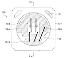
前記課題を解決するために、本発明に係る発光装置は、基体と、前記基体に設けられた導電部材と、前記導電部材の少なくとも一部に設けられた銀含有金属と、前記基体上に載置された発光素子と、前記発光素子および前記銀含有金属の表面において、一部を被覆する絶縁部材と、前記絶縁部材が形成されていない部位を被覆するように設けられる絶縁性のフィラーと、を備えることを特徴とする。 In order to solve the above problems, a light-emitting device according to the present invention is mounted on a base, a conductive member provided on the base, a silver-containing metal provided on at least a part of the conductive member, and the base. In the surface of the light emitting element placed, the light emitting element and the silver-containing metal, an insulating member that covers a part, an insulating filler that is provided so as to cover a portion where the insulating member is not formed, It is characterized by providing.
かかる構成によれば、発光装置は、導電部材に設けられた銀含有金属等に絶縁部材が被覆されている。このように導電部材の表面に、光取り出し効率を高めるために銀含有金属を設けたとしても、絶縁部材により、銀を大気中の硫化ガス等の腐食ガスから保護することができる。そのため、高出力化するために利用する銀が腐食ガスにより変色することを防止し、信頼性や寿命を向上させることができる。また、発光装置は、導電部材の表面において、絶縁部材が形成されていない部位が、絶縁性のフィラーで被覆されている。このような構成にすることで、絶縁部材が形成されていない部位を大気中の硫化ガス等から保護することができる。また、銀含有金属が腐食ガスにより劣化された場合、例えば銀含有金属が硫化された場合であっても、発光素子の発光を絶縁性のフィラーにより反射することで光取り出し効率の低下を抑制することができる。ここで、「基体上」とは、基体の上側にあることを指し、発光素子は導電部材及び/又は銀含有金属を介して載置することができる。 According to this configuration, in the light emitting device, the insulating member is covered with the silver-containing metal or the like provided on the conductive member. Thus, even if a silver-containing metal is provided on the surface of the conductive member in order to increase the light extraction efficiency, the insulating member can protect silver from corrosive gases such as sulfide gas in the atmosphere. Therefore, it is possible to prevent the silver used for increasing the output from being discolored by the corrosive gas, and to improve the reliability and life. Further, in the light emitting device, a portion where the insulating member is not formed is covered with an insulating filler on the surface of the conductive member. By adopting such a configuration, it is possible to protect a portion where the insulating member is not formed from a sulfide gas or the like in the atmosphere. Further, when the silver-containing metal is deteriorated by the corrosive gas, for example, even when the silver-containing metal is sulfided, the light emission efficiency is suppressed by reflecting the light emitted from the light-emitting element by the insulating filler. be able to. Here, “on the substrate” means being on the upper side of the substrate, and the light emitting element can be mounted via a conductive member and / or a silver-containing metal.
また、前記絶縁性のフィラーは、前記発光素子の外周領域を被覆するように設けられていることが好ましい。
かかる構成によれば、光取り出し効率がよくなり光出力を向上させることができる。
Moreover, it is preferable that the said insulating filler is provided so that the outer peripheral area | region of the said light emitting element may be coat | covered.
According to this configuration, the light extraction efficiency is improved and the light output can be improved.
前記絶縁性のフィラーは、前記発光素子の下部領域を被覆するように設けられていることが好ましい。
かかる構成によれば、光取り出し効率がよくなり光出力を向上させることができる。
It is preferable that the insulating filler is provided so as to cover a lower region of the light emitting element.
According to this configuration, the light extraction efficiency is improved and the light output can be improved.
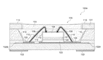
前記導電部材の電極となる部位と前記発光素子の電極端子とを電気的に接続するワイヤを有し、前記ワイヤの上面に前記絶縁部材が形成されており、前記ワイヤの下面に前記絶縁性のフィラーが形成されていることが好ましい。
かかる構成によれば、発光装置は、フィラーがワイヤの裏面(下面)を被覆することにより、発光素子からワイヤ裏面に直接照射される光がワイヤに吸収されることによる光の吸収量を低減することができる。そのため、光取り出し効率がよくなり光出力を向上させることができる。
A wire that electrically connects a portion to be an electrode of the conductive member and an electrode terminal of the light emitting element; the insulating member is formed on an upper surface of the wire; and the insulating material is formed on a lower surface of the wire. It is preferable that a filler is formed.
According to such a configuration, in the light emitting device, the filler covers the back surface (lower surface) of the wire, thereby reducing the amount of light absorbed when the light directly irradiated from the light emitting element to the back surface of the wire is absorbed by the wire. be able to. Therefore, the light extraction efficiency is improved and the light output can be improved.
また、前記ワイヤの下面に形成される絶縁性のフィラーの反射率は、430nm〜490nmの波長域の光に対して50%以上であることが好ましく、70%以上であることがさらに好ましい。 Further, the reflectance of the insulating filler formed on the lower surface of the wire is preferably 50% or more, and more preferably 70% or more with respect to light in the wavelength region of 430 nm to 490 nm.
かかる構成によれば、発光装置は、430nm〜490nmの波長域の光を効率良く反射することができる。そのため、発光スペクトルのピーク波長が上記のような範囲の発光素子を用いる場合に光取り出し効率がよくなり光出力を向上させることができる。 According to this configuration, the light emitting device can efficiently reflect light in the wavelength range of 430 nm to 490 nm. Therefore, when a light emitting element having a peak wavelength of the emission spectrum as described above is used, the light extraction efficiency is improved and the light output can be improved.
また、前記発光素子の下面側に、当該発光素子の下面よりも面積が小さい接着層を備えることが好ましい。ここで、発光素子の下面とは、発光素子を構成する半導体層が積層される基板と言い換えることもできるため、その基板の面積よりも接着層の面積が小さいと言ってもよい。 Moreover, it is preferable that an adhesive layer having a smaller area than the lower surface of the light emitting element is provided on the lower surface side of the light emitting element. Here, the lower surface of the light-emitting element can also be referred to as a substrate on which a semiconductor layer included in the light-emitting element is stacked. Therefore, the area of the adhesive layer may be smaller than the area of the substrate.
かかる構成によれば、たとえ、反射層の側面やその下方の周囲等に絶縁部材を形成することができなかったとしても、その絶縁部材が形成されていない部位が、フィラーで被覆されるため、このフィラーで接着層の側面やその下方の周囲等を保護すると共に、発光素子の下方に進む光を効率よく反射することができる。また、絶縁部材が形成されていない部位における銀含有金属が腐食ガスにより硫化されたとしても、絶縁性のフィラーにより、発光素子からの光を反射することができるため、発光装置の光出力への悪影響を低減し、高出力の発光装置を得ることができる。 According to such a configuration, even if the insulating member could not be formed on the side surface of the reflective layer or the lower periphery thereof, the portion where the insulating member is not formed is covered with the filler. The filler can protect the side surface of the adhesive layer and the surrounding area under the adhesive layer, and can efficiently reflect the light traveling below the light emitting element. In addition, even if the silver-containing metal in the portion where the insulating member is not formed is sulfided by the corrosive gas, the light from the light emitting element can be reflected by the insulating filler, so that the light output to the light emitting device can be reduced. An adverse effect is reduced and a high-output light-emitting device can be obtained.
また、前記課題を解決するために、本発明に係る別の発光装置は、基体と、前記基体に設けられた導電部材と、前記基体上に載置された発光素子と、前記導電部材の電極となる部位と前記発光素子の電極端子とを電気的に接続するワイヤと、前記発光装置を上から被覆するように設けられた絶縁部材と、前記発光装置の表面において前記絶縁部材が形成されていない導電部位を被覆するように設けられる絶縁性のフィラーと、を備えることを特徴とする。ここで、絶縁膜は、発光装置の中で少なくともワイヤの表面を被覆しており、ワイヤの該絶縁部材が形成されていない部位であるワイヤの下面を絶縁性のフィラーで被覆している。 In order to solve the above problems, another light emitting device according to the present invention includes a base, a conductive member provided on the base, a light emitting element placed on the base, and an electrode of the conductive member. A wire for electrically connecting the portion to the electrode terminal of the light emitting element, an insulating member provided to cover the light emitting device from above, and the insulating member formed on the surface of the light emitting device. And an insulating filler provided so as to cover a non-conductive part. Here, the insulating film covers at least the surface of the wire in the light emitting device, and covers the lower surface of the wire, which is a portion where the insulating member of the wire is not formed, with an insulating filler.
かかる構成によれば、発光装置は、フィラーがワイヤの下面を被覆することにより、発光素子からワイヤ裏面に直接照射される光がワイヤに吸収される吸収量を低減することができる。そのため、光取り出し効率がよくなり光出力を向上させることができる。 According to such a configuration, the light emitting device can reduce the amount of absorption by which the light directly irradiated from the light emitting element to the back surface of the wire is absorbed by the wire by covering the lower surface of the wire with the filler. Therefore, the light extraction efficiency is improved and the light output can be improved.
また、前記フィラーは、SiO2、Al2O3、Al(OH)3、TiO2、ZrO2、ZnO2、Nb2O5、MgO、MgCO3、Mg(OH)2、SrO、In2O3、TaO2、HfO、SeO、Y2O3、SiN、AlN、AlON、MgF2からなる群から選択されることが好ましい。 Further, the filler is, SiO 2, Al 2 O 3 , Al (OH) 3, TiO 2, ZrO 2, ZnO 2, Nb 2 O 5, MgO, MgCO 3, Mg (OH) 2, SrO, In 2 O 3 , preferably selected from the group consisting of TaO 2 , HfO, SeO, Y 2 O 3 , SiN, AlN, AlON, and MgF 2 .
かかる構成によれば、光取り出し効率がよくなり光出力を向上させることができる。 According to this configuration, the light extraction efficiency is improved and the light output can be improved.
また、前記フィラーは、前記絶縁部材と異なる材料からなることが好ましい。絶縁部材には、フィラーよりも屈折率が低いものを用いる。また、フィラーには絶縁部材よりも屈折率が高いものを用いるのがよい。絶縁部材には、発光素子からの光を透過させる部材を用いる。また、フィラーには発光素子からの光を散乱させるものを用いることによって、発光装置の光取り出し効率や信頼性を向上させることができる。 Moreover, it is preferable that the said filler consists of a material different from the said insulating member. An insulating member having a refractive index lower than that of the filler is used. In addition, it is preferable to use a filler having a refractive index higher than that of the insulating member. As the insulating member, a member that transmits light from the light emitting element is used. In addition, by using a filler that scatters light from the light emitting element, light extraction efficiency and reliability of the light emitting device can be improved.
また、前記発光装置は、封止部材により被覆されており、前記絶縁性のフィラーの隙間には該封止部材が含浸していることが好ましい。これによりフィラーと封止部材との密着力を向上させることができる。 Moreover, it is preferable that the light emitting device is covered with a sealing member, and the sealing member is impregnated in a gap between the insulating fillers. Thereby, the adhesive force of a filler and a sealing member can be improved.
また、前記課題を解決するために、本発明の発光装置の製造方法は、銀含有金属で少なくとも一部が被覆された導電部材が設けられた基体に発光素子を接合するダイボンディング工程と、前記発光素子および前記銀含有金属の表面の一部に絶縁部材を形成する絶縁部材形成工程と、前記絶縁部材が形成されていない部位に絶縁性のフィラーを形成するフィラー形成工程と、を有することを特徴とする。 In order to solve the above problems, a method for manufacturing a light-emitting device according to the present invention includes a die bonding step of bonding a light-emitting element to a substrate provided with a conductive member at least partially coated with a silver-containing metal, An insulating member forming step of forming an insulating member on a part of the surface of the light emitting element and the silver-containing metal, and a filler forming step of forming an insulating filler in a portion where the insulating member is not formed. Features.
かかる手順によれば、発光装置の製造方法は、絶縁部材形成工程にて、絶縁部材を形成するので、光取り出し効率を高めるために、導電部材の表面に銀含有金属を用いたとしても、成膜した絶縁部材により、銀を大気中の硫化ガス等から保護することができる。そして、発光装置の製造方法は、絶縁部材の成膜においてピンホール等が生じたとしても、フィラーにより絶縁部材が形成されていない銀含有金属を大気中の硫化ガス等から保護することができる。そのため、発光装置の信頼性や生産性を向上させることができる。さらに、このフィラーは、絶縁部材が形成されていない部位に形成されることにより、この部位においても、発光素子の発光をフィラーにより反射することで光取り出し効率を高めることもできる。 According to such a procedure, the light emitting device manufacturing method forms the insulating member in the insulating member forming step. Therefore, even if a silver-containing metal is used on the surface of the conductive member in order to increase the light extraction efficiency, Silver can be protected from sulfide gas or the like in the atmosphere by the filmed insulating member. And even if a pinhole etc. arise in the film formation of an insulating member, the manufacturing method of a light-emitting device can protect the silver containing metal in which the insulating member is not formed with a filler from the sulfide gas etc. in air | atmosphere. Therefore, the reliability and productivity of the light emitting device can be improved. Furthermore, since the filler is formed in a portion where the insulating member is not formed, the light extraction efficiency can be increased by reflecting the light emitted from the light emitting element by the filler also in this portion.
また、前記ダイボンディング工程の後に、前記銀含有金属を介して前記導電部材の電極となる部位と前記発光素子の電極端子とをワイヤにより電気的に接続するワイヤボンディング工程を有し、前記絶縁部材形成工程において、前記発光素子、前記銀含有金属および前記ワイヤの少なくとも一部を上から被覆するように絶縁部材を形成し、前記フィラー形成工程において、前記絶縁部材が形成されていない部位を被覆するように絶縁性のフィラーを電着塗装法または静電塗装法により形成することが好ましい。ここで、前記絶縁部材が形成されていない部位とは、発光素子の外周部や下部、またはその近傍にある部材、さらには銀含有金属の露出面やワイヤの下面のような絶縁部材が形成されない部位や絶縁部材が形成されにくい部位等である。 In addition, after the die bonding step, the insulating member includes a wire bonding step of electrically connecting a portion serving as an electrode of the conductive member and an electrode terminal of the light emitting element through the silver-containing metal with a wire. In the forming step, an insulating member is formed so as to cover at least a part of the light emitting element, the silver-containing metal, and the wire from above, and in the filler forming step, a portion where the insulating member is not formed is covered. Thus, it is preferable to form the insulating filler by an electrodeposition coating method or an electrostatic coating method. Here, the portion where the insulating member is not formed is a member in the outer peripheral portion or the lower portion of the light emitting element or in the vicinity thereof, and further, the insulating member such as the exposed surface of the silver-containing metal or the lower surface of the wire is not formed. This is a site where it is difficult to form a site or an insulating member.
かかる手順によれば、発光装置の製造方法は、例えば絶縁部材が形成されていないワイヤの下面(裏面)にも、フィラーを形成することができる。これにより、発光素子からワイヤ裏面に直接照射される光がワイヤに吸収される吸収量を低減することができる。そのため、発光装置は、光取り出し効率がよくなり光出力を向上させることができる。 According to such a procedure, the manufacturing method of the light emitting device can form the filler also on the lower surface (back surface) of the wire on which the insulating member is not formed, for example. Thereby, the absorption amount by which the light directly irradiated from the light emitting element to the back surface of the wire is absorbed by the wire can be reduced. Therefore, the light emitting device can improve the light extraction efficiency and improve the light output.
本発明の発光装置によれば、銀含有金属の表面を絶縁部材および絶縁性のフィラーで被覆することで、この銀含有金属を保護すると共に、絶縁性のフィラーを備えることにより発光素子からの光を効率良く外部に取り出すことができるので、高出力かつ高信頼性を実現できる。
本発明の発光装置の製造方法によれば、銀含有金属の表面を絶縁部材で保護すると共に、この絶縁部材で保護されていない部位には絶縁性のフィラーを形成するので、高出力かつ高信頼性の発光装置を製造することができる。
According to the light-emitting device of the present invention, the surface of the silver-containing metal is covered with the insulating member and the insulating filler, thereby protecting the silver-containing metal and providing the insulating filler with the light from the light-emitting element. Can be efficiently taken out to the outside, so that high output and high reliability can be realized.
According to the method for manufacturing a light-emitting device of the present invention, the surface of the silver-containing metal is protected with an insulating member, and an insulating filler is formed in a portion that is not protected with the insulating member. Light-emitting device can be manufactured.
本発明を実施するための形態を、以下に図面を参照しながら説明する。ただし、以下に示す実施形態は、本発明の技術思想を具体化するための発光装置およびその製造方法を例示するものであって、本発明は、発光装置およびその製造方法を以下に限定するものではない。また、同一の名称、符号については同一または同質の部材を示しており、詳細説明を適宜省略する。 A mode for carrying out the present invention will be described below with reference to the drawings. However, the embodiment described below exemplifies a light emitting device and a manufacturing method thereof for embodying the technical idea of the present invention, and the present invention limits the light emitting device and the manufacturing method thereof to the following. is not. Moreover, the same name and code | symbol have shown the member same or the same quality, and abbreviate | omits detailed description suitably.
以下では、1.発光装置の構成の概略、2.発光装置の製造方法、3.発光装置を構成する各部材の各章に分けて順次説明する。 In the following, 1. 1. Outline of configuration of light emitting device 2. Manufacturing method of light emitting device Each of the members constituting the light-emitting device will be described in order in each chapter.
[1.発光装置の構成の概略]
本発明の実施形態に係る発光装置の構成の概略について図1〜図3を適宜参照して説明する。図1に示す発光装置100は、その基体101が、例えば積層された複数のセラミックスグリーンシートを焼成して構成されている。基体101は、凹部109を有している。凹部109は、上面が開口し、側面と底面とを有する。凹部109に発光素子104(図2参照)が載置されている。また発光素子104が載置された凹部109は、樹脂等からなる封止部材108で封止されている。
[1. Outline of configuration of light emitting device]
An outline of a configuration of a light emitting device according to an embodiment of the present invention will be described with reference to FIGS. In the
図2は、発光装置100を発光面側から封止部材108を透過して見た平面図を示す。凹部109の底面には、電極としての導電部材102A、102Bが露出するように配されている。図2に示すように、凹部109の底面に露出した導電部材102Aはカソード(−極)であり、凹部109の底面に露出した導電部材102Bはアノード(+極)である。カソード側の導電部材102Aの上には、電子部品としての半導体発光素子(以下、発光素子)104と保護素子105とが設けられている。発光素子104の正負の電極(電極端子)は、導電性のワイヤ106により、導電部材102A、102Bにそれぞれ電気的に接続されている。
FIG. 2 is a plan view of the
保護素子105は、例えば、ツェナーダイオード等から構成される。保護素子105は、その底面側の正極が金属ペースト等の接合部材によって導電部材102Aに固定されて導通し、負極がワイヤ106により導電部材102Bに電気的に接続されている。なお、基体101の上面には、導電部材102A、102Bのいずれがカソード側であるのかを示すためにカソードマーク107が設けられている。なお、カソードマークの代わりにアノードマークを設けて発光装置100の極性を示すようにしてもよい。この保護素子105は、省略することもできる。
The
図3に示すように、導電部材102A、102Bは、外部と電気的に接続する端子として機能させるために、基体101の下面(裏面)にも露出するように設けられている。基体101の裏面に配された導電部材102Aは、凹部109の底面に配された導電部材102Aに基体101内部で電気的に連続するように設けられている。同様に、基体101の裏面に配された導電部材102Bは、凹部109の底面に配された導電部材102Bに基体101内部で電気的に連続するように設けられている。そして、凹部109の底面にそれぞれ露出している導電部材102A、102Bの表面には、反射材としての銀含有金属103が鍍金等により設けられている。また、凹部109の底面に設けられた銀含有金属103の表面には、接着層123を介して発光素子104が設けられており、それ以外の銀含有金属103の表面は絶縁部材110で被覆されている。また、絶縁部材110が成膜されずに銀含有金属103が露出した部位には絶縁性のフィラー112が形成されている。特に発光素子104の下部領域は、銀含有金属103が露出した部位を含めて絶縁性のフィラー112で被覆されている。
As shown in FIG. 3, the conductive members 102 </ b> A and 102 </ b> B are provided so as to be exposed also on the lower surface (back surface) of the base 101 in order to function as terminals electrically connected to the outside. The conductive member 102 </ b> A disposed on the back surface of the
発光素子104は、例えば、図4に示すように、基板104aと、基板104aに順次積層された発光層等の積層半導体構造104bと、積層半導体構造104bの上に形成された電極端子104cとを有する。なお、発光素子104の正負の電極端子は、異なる半導体層を露出した表面に設けられる。
For example, as shown in FIG. 4, the
また、発光素子104の下面(裏面)には、例えば、パターニングされたAg/Pt/AuSn膜を成膜することができる。図3に示す例では、発光素子104と基体101との間には、発光素子104の下面側から順に、例えばAgから成る反射層121と、Ptから成るバリア層122と、ダイボンド部材として金属共晶であるAuSnからなる接着層123とが配されている。発光素子104の下面側に配された反射層121、バリア層122、接着層123の面積は、発光素子104(図4参照)の裏面の面積よりも小さい。
Further, for example, a patterned Ag / Pt / AuSn film can be formed on the lower surface (back surface) of the
発光素子104は、例えば、凹部109の底面に塗布されたフラックスの上に載置されるダイボンディング工程と、これに続くリフロー工程、洗浄工程を経た後、各ワイヤ106が凹部109の底面に配された導電部材102A、102Bの表面の銀含有金属103とそれぞれ接続される。
For example, after the
発光装置100は、上述したように、基体101の凹部109内に、導電部材102A、102Bの表面上の銀含有金属103を主として保護する絶縁部材110を備えている。この絶縁部材110は、凹部109内において、銀含有金属103に加えて、発光素子104、ワイヤ106、基体101の表面(凹部109の底面や側面)を上から被覆するように設けられている。また、絶縁部材110は、凹部109以外にも基体101の上面を被覆してもよい。
As described above, the
また、発光装置100は、上述したように、基体101の凹部109に配された銀含有金属103の露出面を被覆するように絶縁性のフィラー112を備えている。この絶縁性のフィラーは、絶縁部材110と異なる製法により形成される。図3においては、絶縁性のフィラー112は、発光素子104、ワイヤ106、銀含有金属103等の導体部の表面において絶縁部材110が形成されていない部位を被覆するように設けられている。絶縁性のフィラー112は、例えば、発光素子104の下方に位置する銀含有金属103と、発光素子104の下方に配された反射層121、バリア層122、接着層123の側面と、ワイヤ106の下面(裏面)とを被覆する。絶縁性のフィラー112は、主に絶縁部材が形成されていない部位を被覆する。また、絶縁性のフィラー112は、基体101の凹部109に載置されている部材の中で導電性部材の露出面を被覆する。絶縁性のフィラー112は、発光素子104の光を反射する反射膜として機能する。また、前述した絶縁部材110と絶縁性のフィラー112との違いは膜構造である。絶縁性のフィラー112の膜構造は、フィラーの粒子が連結して堆積したものであり、堆積したフィラーの間には空隙が形成されている。フィラーの隙間には封止部材が含浸されやすくなり、フィラーと封止部材との密着力を向上させることができる。一方、絶縁部材は、フィラーに比べて密に形成されている。これにより、絶縁部材は、透過率を向上させており、優れたガスバリア性の機能を有している。
Further, as described above, the
このように発光装置100は、導電部材102A、102Bに設けられた銀含有金属103が絶縁部材110で被覆され、かつ、絶縁部材110が形成されていない導体部が、絶縁性のフィラー112で被覆されている。そのため、絶縁性のフィラーを1μm以上の膜厚で形成する。この絶縁性のフィラーを10μm以上の膜厚で形成した場合には、銀含有金属を大気中の硫化ガス等の腐食ガスから保護する効果と光の散乱効果を有する。また、絶縁部材が形成されていない部位における銀含有金属が腐食ガスにより硫化されたとしても、絶縁性のフィラーにより、発光素子からの光を反射することができるため、外部に効率よく光を取り出すことができる。
As described above, in the
さらに、発光装置100は、ワイヤ106の裏面が、高反射率の絶縁性のフィラー112により被覆されているので、ワイヤ106の下方に配置された発光素子104を発光させたときに、ワイヤ106の裏面側において光吸収量を低減させることができる。このとき、ワイヤ106の裏面を被覆している絶縁性のフィラー112は、発光素子104の発光を反射するので、外部に効率よく光を取り出すことができる。以上の動作により、高出力、高信頼性、長寿命の発光装置を実現することができる。
Furthermore, since the back surface of the
[2.発光装置の製造方法]
次に、本発明の実施形態に係る発光装置の製造方法について説明する。図1〜図3に示す発光装置100は、例えば、図4〜図8に示す製造工程を経て得ることができる。すなわち、発光装置の製造方法は、主として、ダイボンディング工程(図4参照)と、ワイヤボンディング工程(図5参照)と、フィラー形成工程(図7参照)とを有する。さらに、封止部材108を形成する場合には、封止部材形成工程(図8参照)を行う。
[2. Manufacturing method of light emitting device]
Next, a method for manufacturing a light emitting device according to an embodiment of the present invention will be described. The
ダイボンディング工程(図4参照)は、発光素子104を基体101に接合するためのダイボンド部材の種類や接合方法等に応じて様々な方法で行うことができる。ここで、ダイボンディング工程は、基体101と、発光素子104とが既に製造されていることを前提としている。ただし、例えば、ダイボンディング工程の前に、基体101に導電部材102A、102Bを設ける工程や、導電部材102A、102B上に銀含有金属103を設ける工程を行ってもよい。このうち、基体101に導電部材102A、102Bを設ける工程は、基体101の材料や導電部材102A、102Bの材料等に応じて様々な方法で行うことができ、かつ、ダイボンディング工程で用いる方法とも密接に関連している。
The die bonding step (see FIG. 4) can be performed by various methods depending on the type of the die bonding member for bonding the
ここでは、発光装置100の製造方法を、第1工程〜第6工程に形式的に区分し、銀含有金属形成工程(第1工程)、ダイボンディング工程(第2工程)、ワイヤボンディング工程(第3工程)、絶縁部材形成工程(第4工程)、フィラー形成工程(第5工程)、封止部材形成工程(第6工程)について順次説明する。
Here, the manufacturing method of the
また、簡便のため、1つの発光装置100を用いて図4〜図8を適宜参照しながら各製造工程を説明するが、これらの製造工程では、複数の発光装置の基体が集合体となっている。そして、基体の集合体を最終工程で分割した後で、各発光装置100の基体101の外側面が表出する。
For convenience, each manufacturing process will be described using one light-emitting
<2−1.第1工程(銀含有金属形成工程)>
第1工程は、発光装置100の導電部材102A、102B上に銀含有金属103を設けるまでの工程である。ここでは、2−1−A.導電部材形成工程と、2−1−B.銀鍍金工程とを行う。
<2-1. First step (silver-containing metal forming step)>
The first step is a step until the silver-containing
≪2−1−A.導電部材形成工程≫
図4に示すように、本実施形態において発光装置100の基体101は凹部109を有している。基体101の凹部109の底面には、導電部材102A、102Bが露出するように形成する。
<< 2-1-A. Conductive member formation process >>
As shown in FIG. 4, in this embodiment, the
なお、この導電部材102A、102Bは、通電させるための電極として用いる以外に、例えば凹部109の内側の側壁に設けて反射部材としての機能を付与させることもできる。また、導電部材102A、102Bは、基体101の裏面から露出させて放熱部材としての機能を付与させることもできる。基体101の裏面から露出させる導電部材102A、102Bは、電極としての機能を兼ね備えることもできる。また、電極として用いる導電部材と、放熱部材として用いる導電部材とを電気的には遮断させることもできる。また、導電部材は、図2に示すように、発光装置100の極性を示すカソードマーク107として設けることもできる。
The
このような導電部材102A、102Bを形成する方法は、基体101の材料等に応じて適宜変更できる。例えばセラミックスからなる基体101を用いる場合、未焼成のセラミックスグリーンシートの段階で、タングステン、モリブデンのような高融点金属の微粒子を含む導体ペーストを所定のパターンに塗布したものを焼成することにより、導電部材102A、102Bを得ることができる。また、予め焼成されたセラミックスの板材に、導電部材102A、102Bを形成することもできる。
The method of forming such
また、例えば、基体101としてガラスエポキシ樹脂基板を用いる場合には、次のようにして導電部材102A、102Bを形成することもできる。この場合、まず、硝子クロス入りエポキシ樹脂やエポキシ樹脂を半硬化させたプリプレグに銅板を貼り付けて熱硬化させる。その後、フォトリソグラフィ法を用いて銅等の金属部材を所定の形状にパターニングする。これにより、基体101中に導電部材102A、102Bを形成することができる。
For example, when a glass epoxy resin substrate is used as the
≪2−1−B.銀鍍金工程≫
続いて、前記のようにして形成された導電部材102A、102B上に、銀含有金属103を設ける。なお、基体101内に埋設されている導電部材上にまでは銀含有金属103を設けるものではない。
<< 2-1-B. Silver plating process >>
Subsequently, the silver-containing
銀含有金属103を設ける方法としては、鍍金法を用いるが、その他にも、スパッタ法、蒸着法等を用いることができる。鍍金法を用いる場合、電解鍍金、無電解鍍金いずれの方法でも用いることができる。例えば、導電部材102A、102B上のみに銀含有金属103を設ける場合には、該当部位を電気的に接続した上で、電解鍍金法を用いることが最も簡便である。また、無電解鍍金法やスパッタ法、蒸着法を用いる場合は、フォトリソグラフィ法により、導電部材102A、102B上のみに設けることができる。
As a method for providing the silver-containing
銀含有金属103は、母体となる導電部材102A、102Bの上に直接設けてもよく、または、銀を含まない金属を介して、導電部材102A、102Bの上に間接的に設けてもよい。また、特にパターン形成されていない導電部材102A、102B上に銀含有金属103を設けた後、導電部材102A、102Bと銀含有金属103とを所定の形状にパターニングしてもよい。この銀含有金属103は、導電部材102A、102Bの表面の少なくとも一部が被覆されていればよいが、後の工程であるダイボンディング工程において、発光素子が載置される領域下部に位置する導電部材102の表面には銀含有金属103が全面を被覆していることが好ましい。これにより、発光素子から下方に放出される光を光取り出し面である上方に反射させることができる。
The silver-containing
<2−2.第2工程(ダイボンディング工程)>
第2工程は、発光装置100の導電部材102A、102B上にダイボンド部材を介して発光素子104を接合する工程である。ここでは、2−2−A.ダイボンド部材形成工程と、2−2−B.加熱工程とを行う。ここで、ダイボンド部材は特に材料を限定するものではないが、樹脂組成物で形成することができる。
<2-2. Second process (die bonding process)>
The second step is a step of bonding the
≪2−2−A.ダイボンド部材形成工程≫
ダイボンド部材は、導電部材102A、102Bと発光素子104との間に介在するように形成すればよい。そのため、ダイボンド部材を形成する部位は、次の(A1)〜(A3)のいずれでもよい。
(A1)導電部材102A、102B上のうち発光素子104を載置する領域
(A2)発光素子104の裏面
(A3)A1とA2の両方
<< 2-2-A. Die bond member formation process >>
The die bond member may be formed so as to be interposed between the
(A1) Region on which the
ダイボンド部材としては、樹脂組成物がある。その樹脂組成物の成分には、例えば、ロジン(松脂)または熱硬化性樹脂を含む。さらに、樹脂組成物に、必要に応じて、粘度調整のための溶剤や各種添加剤、有機酸等の活性剤を含有させてもよい。さらにまた、粉末状の金属を含有させてもよい。また、樹脂組成物の形状は、液状、ペースト状、固体状(シート状、ブロック状、粉末状)のものを用いることができ、樹脂組成物の組成や基体101の形状等に応じて、樹脂組成物の形状を適宜選択することができる。
There exists a resin composition as a die-bonding member. The component of the resin composition includes, for example, rosin (pine resin) or a thermosetting resin. Furthermore, you may make the resin composition contain activators, such as a solvent for viscosity adjustment, various additives, and an organic acid, as needed. Furthermore, a powdered metal may be contained. The resin composition can be in the form of a liquid, paste, or solid (sheet, block, or powder). Depending on the composition of the resin composition or the shape of the
次に、樹脂組成物を形成する部位が、前記した(A1)導電部材102A、102B上のうち発光素子104を載置する領域である場合について、樹脂組成物の形成方法および樹脂組成物(フラックスまたは半田)を介した接合方法について説明する。
Next, the resin composition forming method and the resin composition (flux) in the case where the portion where the resin composition is formed is a region where the
まず、図4に示すように、導電部材102A、102B上に設けられた銀含有金属103上に、ダイボンド部材となる液状またはペースト状の樹脂組成物111が形成される。このように導電部材102A、102B上に、液状またはペースト状の樹脂組成物111を形成する方法は、樹脂組成物111の粘度等に応じて、ポッティング法、印刷法、転写法等の方法から適宜選択することができる。続いて、樹脂組成物111を形成した箇所に発光素子104を載置する。固体状の樹脂組成物を設ける場合も、発光素子104を載置するのと同じ要領で絶縁部材上に設置する等の方法を用いることができる。液状、ペースト状、固体状の樹脂組成物は、加熱等により一度溶融させることで発光素子104を固定させてもよい。また、樹脂組成物は、単独で用いてもよく、または、組み合わせて用いてもよい。
First, as shown in FIG. 4, a liquid or paste-like resin composition 111 to be a die bond member is formed on the silver-containing
樹脂組成物の量としては、発光素子104を設置した後に、載置されている発光素子104の接合面積と同等か、それ以上の面積となるように調整して樹脂組成物を形成することが好ましい。また、複数の発光素子104を液状またはペースト状の樹脂組成物111の上に載置する場合には、液状またはペースト状の樹脂組成物111の表面張力等により発光素子104が動いて所定の位置からずれてしまう場合がある。そのため、このような事態を防ぐため、各発光素子104を、個別に独立した樹脂組成物111にそれぞれ載置する方が望ましい。
The amount of the resin composition may be adjusted to be equal to or larger than the bonding area of the mounted
図4に示すように、ダイボンド部材である樹脂組成物111の量は、載置される発光素子104の接合面積よりも広い面積となるように調整して樹脂組成物111を形成した。この場合、発光素子104の載置後には、樹脂組成物111は、発光素子104の下部に設けられた接着層123の接合面積よりも広がった状態となる。
As shown in FIG. 4, the resin composition 111 was formed by adjusting the amount of the resin composition 111 that is a die-bonding member to be larger than the bonding area of the light-emitting
また、樹脂組成物の厚みについては、樹脂組成物の種類によって適した厚みが異なることを考慮して調整することが好ましい。また、樹脂組成物の厚みについては、発光素子104を載せた際に樹脂組成物が押し潰されてそのまま横に広がる場合や、樹脂組成物が基体101の凹凸に沿って追従して広がる場合等を考慮して調整することが好ましい。
In addition, the thickness of the resin composition is preferably adjusted in consideration that the suitable thickness varies depending on the type of the resin composition. As for the thickness of the resin composition, when the
また、発光素子104の材料や接合方法等に応じては、樹脂組成物に導電性のある部材を含有させることが好ましい。例えば、次の具体例B1,B2を挙げることができる。
(B1)発光素子の基板104aとして導電性の基板を使用し、窒化ガリウム系半導体層を積層させて積層半導体構造104bを構成して作製された発光素子104を用いて、この窒化ガリウム系半導体発光素子の半導体層に形成された電極または導電性の基板を接合面とする場合
(B2)発光素子の基板104aとして絶縁性の基板を使用し、窒化ガリウム系半導体層を積層させて積層半導体構造104bを構成して作製された発光素子104を用いて、この窒化ガリウム系半導体発光素子の半導体層に形成された電極を接合面とする場合
Further, depending on the material of the light-emitting
(B1) Using a conductive substrate as the substrate 104a of the light-emitting element and laminating gallium nitride-based semiconductor layers to form a laminated semiconductor structure 104b, the gallium nitride-based semiconductor light emitting device is used. When an electrode formed on a semiconductor layer of an element or a conductive substrate is used as a bonding surface (B2) An insulating substrate is used as the substrate 104a of the light emitting element, and a gallium nitride based semiconductor layer is stacked to form a stacked semiconductor structure 104b. In the case where the electrode formed on the semiconductor layer of the gallium nitride based semiconductor light-emitting device is used as a bonding surface using the light-emitting
前記(B1)や(B2)の場合には、基体101に設けられる導電部材102A、102Bと発光素子104とを、その接合部分で導通させる必要がある。したがって、このような場合には、樹脂組成物中に比較的低い融点を有する金属等の導電性のある部材を混入させておくことが好ましい。
In the case of (B1) and (B2), the
≪2−2−B.加熱工程≫
加熱工程は、前記のようにして形成した樹脂組成物の少なくとも一部が揮発する温度より高い温度で加熱するものである。樹脂組成物が含有する物質に応じて加熱温度は異なる。
<< 2-2-B. Heating process >>
In the heating step, heating is performed at a temperature higher than the temperature at which at least a part of the resin composition formed as described above volatilizes. The heating temperature varies depending on the substance contained in the resin composition.
加熱工程において、加熱後に続けて、さらに洗浄工程を行うことができる。特に、ロジンを含有する樹脂組成物の樹脂残渣の大部分または全部を除去したい場合等においては、洗浄工程を行うことが好ましい。 In the heating step, a washing step can be further performed after the heating. In particular, when it is desired to remove most or all of the resin residue of the resin composition containing rosin, it is preferable to perform a washing step.
<2−3.第3工程(ワイヤボンディング工程)>
第3工程は、第2工程において銀含有金属103で被覆された電極としての導電部材102A、102Bと、発光素子104上部にある電極端子とを導電性のあるワイヤ106で電気的に接続する工程であり、図5はこの第3工程が完了した状態を示している。なお、図5に示す接着層123は、図4に示す接着層123が発光素子104の載置により変形したものである。
なお、本形態の発光素子の実装形態は、発光素子の電極を発光観測面方向(支持体と反対側)に向けて実装する形態に限定されることなく、フリップチップ実装でもよい。
<2-3. Third Step (Wire Bonding Step)>
The third step is a step of electrically connecting the conductive members 102 </ b> A and 102 </ b> B as electrodes covered with the silver-containing
In addition, the mounting form of the light emitting element of this embodiment is not limited to the form in which the electrode of the light emitting element is mounted in the light emission observation surface direction (the side opposite to the support), and may be flip chip mounting.
<2−4.第4工程(絶縁部材形成工程)>
第4工程は、第3工程に続いて、銀含有金属103で被覆された導電部材102A、102B上、発光素子104上部およびワイヤ106を上から被覆するように、絶縁性の保護膜である絶縁部材110を設けるものである(図6)。
<2-4. Fourth step (insulating member forming step)>
In the fourth step, following the third step, the insulating member is an insulating protective film so as to cover the
絶縁部材110で被覆された領域の銀含有金属103は、硫化等による銀の変質を抑制することができる。そのため、この第4工程を行う段階において基体101の上面、側面に露出している銀含有金属103と、基体101に設けられた凹部109の内面(底面、側面)に露出している銀含有金属103とを含めた全露出領域のうち、銀を変質させる成分(硫黄成分含有ガス等)が外部から到達し易い位置を被覆するように絶縁部材110を形成することが好ましい。
The silver-containing
なお、第4工程を行う段階において基体101中に埋設されている銀含有金属103(発光素子104の載置領域やワイヤ106の接合領域等に埋設されている銀含有金属103)や基体101の下面(裏面)に露出する銀含有金属103にまで絶縁部材110を設けるものではない。
Note that the silver-containing metal 103 (silver-containing
この絶縁部材110は、銀含有金属103上以外にも設けられていてもよい。例えば、図6に示すように、絶縁部材110は、基体101に設けられた凹部109の底面において、正負の導電部材102A、102Bの間に基体101が露出している基体露出部101A、凹部109の側壁101B、基体101の上面101C等にも設けることができる。
This insulating
絶縁部材110の材料には、後記するように、無機物を用いるのが好ましく、絶縁部材110を形成する方法としては、スパッタ法、蒸着法、イオンプレーティング法等のPVD(Physical Vapor Deposition)法、CVD(Chemical Vapor Deposition)法、溶射、コーティング処理等の成膜方法を用いることができる。また、例えば、真空プロセスにより絶縁部材110を成膜することができる。
As will be described later, it is preferable to use an inorganic material for the material of the insulating
しかし、図6に示すように発光素子104の裏面外周部の一部が銀含有金属103と接していない場合(発光素子104の裏面において反射層121等が形成されていない部位があり、その部位と銀含有金属103との間に隙間を有する場合等)には、絶縁部材110が銀含有金属103を被覆していない領域がある。この絶縁部材110が被覆していない領域に腐食性ガスが侵入した場合、銀含有金属103は腐食性ガスに晒されるため、腐食する虞がある。
また、図6に示すように、絶縁部材110に、種々の原因によりピンホール131等が発生する場合がある。この場合には、ピンホールから腐食性ガスが侵入し銀含有金属103を腐食させる原因となる。さらには、ワイヤ106の裏面もこの絶縁部材110は被覆されにくいため、ワイヤ106の裏面は発光素子からの光を吸収してしまう。
しかしながら、本実施形態に係る発光装置の製造方法では、第4工程の完了後、凹部109を封止する前に、次の第5工程を有するので、このような事態を防ぐことができる。
However, as shown in FIG. 6, when a part of the outer periphery of the back surface of the
In addition, as shown in FIG. 6, pin holes 131 and the like may occur in the insulating
However, since the manufacturing method of the light emitting device according to the present embodiment includes the next fifth step after the fourth step is completed and before the
<2−5.第5工程(フィラー形成工程)>
第5工程は、第4工程において成膜した絶縁部材110が形成されていない部位、かつ、銀等の導体部が露出した部位に、フィラーを形成する。
フィラーは、媒質中を電気泳動しやすい形状および大きさとされていることが好ましい。特に、電解液中での電気泳動について、フィラーの形状は、ほぼ球形の粒子状とされていることが好ましい。フィラーの粒径は、10nmから10μmの範囲であることが好ましい。またフィラーの粒径は、100nmから5μmの範囲とすることで、光の散乱の効果が大きくなるため、より好ましい。
<2-5. Fifth step (filler forming step)>
In the fifth step, a filler is formed in a portion where the insulating
The filler is preferably shaped and sized to facilitate electrophoresis in the medium. In particular, for the electrophoresis in the electrolytic solution, it is preferable that the filler has a substantially spherical particle shape. The particle size of the filler is preferably in the range of 10 nm to 10 μm. Moreover, since the effect of light scattering becomes large by making the particle diameter of a filler into the range of 100 nm to 5 micrometers, it is more preferable.
フィラー形成工程は、フィラーを含む溶液中に、発光装置100を配置させる工程と、上記溶液中における電気泳動により、フィラーを上記発光装置に堆積させる工程と、を具備することで形成される。
The filler forming step is formed by including a step of placing the
電解液によりフィラーを堆積させる方法は、溶液中において、発光装置と対向配置される電極を配置し、この電極に電圧を印加することにより、溶液中で帯電されたフィラーを電気泳動させることで絶縁部材110が形成されていない部位(例えば、発光素子の下部にある接着部材等)や銀含有金属等の導電性部材が露出した部位にフィラーを堆積させるものである。
ここで、フィラーが堆積した厚みは、20μm程度である。
上述したフィラーの電着による形成工程の後、フィラー以外の部材を電着により形成してもよい。
In the method of depositing the filler with the electrolytic solution, an electrode disposed opposite to the light emitting device is disposed in the solution, and voltage is applied to the electrode to cause the filler charged in the solution to be electrophoresed for insulation. The filler is deposited on a portion where the
Here, the thickness on which the filler is deposited is about 20 μm.
After the formation step by electrodeposition of the filler described above, a member other than the filler may be formed by electrodeposition.
フィラーの厚みは、溶液(電解液)中のフィラーの粒径、電気泳動沈着の工程における電圧、その電圧の印加時間などを考慮して決定されるものであるが、本発明の実施形態でのフィラーの堆積する厚みは、1μm以上100μm以下とすることが好ましい。フィラーの堆積する厚みをこの範囲にすることで、フィラーによる散乱効率がよく、光の取り出し効率を向上させることができる。 The thickness of the filler is determined in consideration of the particle size of the filler in the solution (electrolyte), the voltage in the electrophoretic deposition process, the application time of the voltage, and the like in the embodiment of the present invention. The thickness at which the filler is deposited is preferably 1 μm or more and 100 μm or less. By setting the thickness of the filler to be deposited in this range, the scattering efficiency by the filler is good and the light extraction efficiency can be improved.
電着用の電解液には、フィラーを分散させた混合液を用いる。この電解液には、その中を帯電されたフィラーが静電気力を受けて移動することができるものであれば特に材料は限定されない。 As the electrolytic solution for electrodeposition, a mixed solution in which a filler is dispersed is used. The electrolyte is not particularly limited as long as the charged filler can move by receiving electrostatic force.
例えば、電解液にフィラーを溶解させる酸やアルカリ、例えば、アルカリ土類金属のイオン(Mg2+など)を含んだ硝酸を含有させたりすることができる。
また、電解液には金属アルコキシドを含有されてもよい。具体的には、Al、Sn、Si、Ti、Y、Pbあるいはアルカリ土類金属から選択される元素を構成元素として含む有機金属材料である。電解液に含まれる材料としては、その他にも、金属アルコレート、あるいは金属アルコキサイドと有機溶剤とを所定の割合で混合してなるゾル中にフィラーを分散させた混合液を電解液とすることもできる。
その他にも、電解液はイソプロピルアルコールを母液とする溶液に、有機溶剤としてアセトン、有機金属材料としてアルミナゾルおよびフィラーを含有させた混合溶液とすることができる。
For example, an acid or an alkali for dissolving the filler in the electrolytic solution, for example, nitric acid containing ions of alkaline earth metal (such as Mg 2+ ) can be contained.
Further, the electrolytic solution may contain a metal alkoxide. Specifically, it is an organometallic material containing an element selected from Al, Sn, Si, Ti, Y, Pb or an alkaline earth metal as a constituent element. In addition, as a material contained in the electrolytic solution, a mixed solution in which a filler is dispersed in a sol obtained by mixing a metal alcoholate or a metal alkoxide and an organic solvent in a predetermined ratio may be used as the electrolytic solution. it can.
In addition, the electrolytic solution can be a mixed solution in which acetone is used as an organic solvent and alumina sol and a filler are used as an organic metal material in a solution containing isopropyl alcohol as a mother liquor.
<2−6.第6工程(封止部材形成工程)>
第6工程は、発光素子104を被覆する封止部材108を形成し硬化するものである。図8は、凹部109内に封止部材108を充填し、発光素子104を被覆したことを示す図である。このように基体101に凹部109が形成されている場合は、凹部109内に溶融樹脂を注入することで、容易に封止部材108を形成することができる。形成された封止部材108は、加熱や光照射等によって硬化させることができる。封止部材108を硬化する条件は、用いる封止部材108の材料によって適宜選択することができる。なお、封止部材108は単一の部材で形成することもできるし、または、2層以上の複数の層として形成することもできる。
<2-6. Sixth step (sealing member forming step)>
In the sixth step, the sealing
封止部材108を加熱により硬化する場合には、昇温または降温の温度や時間、雰囲気等について、適宜選択することができる。また、封止部材108を光照射により硬化する場合には、光照射時間や照射光の波長等について、用いる封止部材108の材料に応じて適宜選択することができる。また、加熱と光照射の両方を用いても封止部材108を硬化してもよい。
In the case where the sealing
[3.発光装置を構成する各部材]
ここでは、3−1.基体、3−2.導電部材、3−3.銀含有金属、3−4.絶縁部材、3−5.フィラー、3−6.ダイボンド部材、3−7.封止部材、3−8.ワイヤ、3−9.波長変換部材、3−10.発光素子、3−11.接着部材、の各節に分けて、発光装置100を構成する各部材について順次説明する。
[3. Each member constituting the light emitting device]
Here, 3-1. Substrate, 3-2. Conductive member, 3-3. Silver-containing metal, 3-4. Insulating member, 3-5. Filler, 3-6. Die bond member, 3-7. Sealing member, 3-8. Wire, 3-9. Wavelength conversion member, 3-10. Light emitting element, 3-11. Each member constituting the
<3−1.基体>
本実施形態において、基体101は、発光素子104や保護素子105等の電子部品を保護するとともに、これら電子部品に外部からの電流を供給するための導電部材102A,102Bを備えているものである。基体101の材料としては、絶縁性部材が好ましく、発光素子104からの光や外光等が透過しにくい部材が好ましい。また、ある程度の強度を有するものが好ましく、より具体的には、セラミックス(Al2O3、AlN等)、フェノール樹脂、エポキシ樹脂、ポリイミド樹脂、BTレジン(bismaleimide triazine resin)、PPA(ポリフタルアミド)等の樹脂が挙げられる。基体101の材料が樹脂である場合には、ガラス繊維や無機フィラー(SiO2、TiO2、Al2O3等)を混合し、機械的強度の向上や熱膨張率の低減、光反射率の向上等を図ることもできる。
<3-1. Base>
In the present embodiment, the
<3−2.導電部材>
導電部材102A、102Bは、外部と発光素子104とを電気的に接続させるためのものである。導電部材102A、102Bの好ましい材料としては、基体101の材料や基体101の製造方法等に応じて適宜選択することができる。
<3-2. Conductive member>
The
例えば、基体101の材料としてセラミックスを用いる場合には、導電部材102A、102Bの材料は、セラミックスシートの焼成温度にも耐え得る高融点を有する部材が好ましく、タングステンやモリブデンのように高融点を有する金属を用いるのが好ましい。
For example, when ceramic is used as the material of the
また、例えば、基体101の材料としてガラスエポキシ樹脂等を用いる場合には、導電部材102A、102Bの材料は、加工し易い材料が好ましく、具体的には、銅、アルミニウム、金、銀、タングステン、鉄、ニッケル等の金属または鉄−ニッケル合金、りん青銅、鉄入り銅、モリブデン等が挙げられる。
For example, when glass epoxy resin or the like is used as the material of the
また、例えば、基体101が射出成型されたエポキシ樹脂からなる場合には、導電部材102A、102Bの材料は、比較的大きい機械的強度を有する部材が好ましい。また、この場合、導電部材102A、102Bの材料は、打ち抜き加工、エッチング加工、屈曲加工等の加工がし易く、かつ、比較的大きい機械的強度を有する部材が好ましい。具体的には、銅、アルミニウム、金、銀、タングステン、鉄、ニッケル等の金属または鉄−ニッケル合金、りん青銅、鉄入り銅、モリブデン等が挙げられる。
For example, when the
<3−3.銀含有金属>
銀含有金属103は、基体101から露出している導電部材102A、102Bの表面に設けられる。銀含有金属103の形成方法は、鍍金法、スパッタ法、蒸着法等を用いることができる。銀含有金属103の材料としては、銀のみでもよいし、銀と、銅、金、アルミニウム、ロジウム等の光反射率の高い金属との合金、もしくは、銀と光反射率の高い金属との多層膜等でもよい。好ましくは、銀単体で構成する。また、銀含有金属103の膜厚は、発光素子104からの光を効率よく反射可能な膜厚とするのが好ましく、具体的には、1nm〜50μm程度が好ましい。なお、銀含有金属103を多層膜とする場合には、多層膜全体の厚さをこの範囲内とすることが好ましい。
<3-3. Silver-containing metal>
The silver-containing
<3−4.絶縁部材>
絶縁部材110は、主として銀含有金属103上に設けられるものである。絶縁部材110の材料としては、透光性のものが好ましく、また、主として無機化合物を用いることが好ましい。具体的には、SiO2、Al2O3、TiO2、ZrO2、ZnO2、Nb2O5、MgO、SrO、In2O3、TaO2、HfO、SeO、Y2O3等の酸化物や、SiN、AlN、AlON等の窒化物、MgF2等のフッ化物が挙げられる。これらは、単独で用いてもよいし、または、混合して用いてもよい。もしくは、積層させるようにしてもよい。
<3-4. Insulating material>
The insulating
絶縁部材110の膜厚については、封止部材108/絶縁部材110の界面や、絶縁部材110/銀含有金属103の界面において多重反射で光の損失が起きないように薄くすることが好ましい一方で、硫黄等のガスが通過しない程度の厚みも必要である。絶縁部材110として用いる材料の種類によって膜厚の好ましい範囲は多少異なるが、絶縁部材110の膜厚は、約1nm〜10μm程度であることが好ましい。絶縁部材110を多層とする場合には、層全体の膜厚がこの範囲内となるようにすることが好ましい。また、硫黄等のガスが通過しにくいよう、絶縁部材110を緻密な膜として形成することが好ましい。
As for the film thickness of the insulating
<3−5.フィラー>
フィラー112は、主に銀含有金属103の露出面において、絶縁部材110が形成されていない部位を被覆することで、銀含有金属103の劣化を効果的に抑制するものである。また、絶縁部材が形成されていない部位における銀含有金属が腐食ガスにより硫化されたとしても、フィラーには発光素子からの光や封止樹脂内で波長変換された光に対して反射率が大きいものが用いられるため、銀含有金属103上部のフィラーにより発光素子からの光を反射することができる。
<3-5. Filler>
The
フィラーは、白色フィラーであることが好ましく、有機フィラーや無機フィラーを用いることができる。フィラーには、有機フィラーとしては、例えば、ポリスチレン系樹脂、スチレン−アクリル共重合体系樹脂、尿素系樹脂、メラミン系樹脂、アクリル系樹脂、塩化ビニリデン系樹脂、ベンゾグアナミン系樹脂などからなるフィラーが挙げられる。また、無機フィラーとしては、具体的には、例えば、酸化チタン、酸化アルミニウム、水酸化アルミニウム、炭酸マグネシウム、水酸化マグネシウムなどが挙げられる。これらの中でも、隠蔽性が高く、高い拡散反射率が得られる酸化チタンが好ましい。これらは、単一材料を用いてもよいし、または、混合材料として用いてもよい。もしくは、積層させて形成してもよい。
また、ワイヤ106の下面に形成されるフィラー112は、その反射率が、430nm〜490nmの波長域の光(青色光)に対して50%以上であることが好ましい。
The filler is preferably a white filler, and an organic filler or an inorganic filler can be used. Examples of the organic filler include fillers made of polystyrene resin, styrene-acrylic copolymer resin, urea resin, melamine resin, acrylic resin, vinylidene chloride resin, benzoguanamine resin, and the like. . Specific examples of the inorganic filler include titanium oxide, aluminum oxide, aluminum hydroxide, magnesium carbonate, and magnesium hydroxide. Among these, titanium oxide is preferable because of its high concealability and high diffuse reflectance. These may be used as a single material or as a mixed material. Alternatively, they may be laminated.
The
<3−6.ダイボンド部材>
ダイボンド工程に用いるダイボンド部材としては、その上に載置される発光素子104を接着固定できるものであれば、特に限定されるものではないが、例えば樹脂組成物を用いる。このダイボンド部材は、基体101の凹部109内の導電部材102A、102B上に銀含有金属103を介して発光素子104や保護素子105等を接合させるための接合部材である。
<3-6. Die Bond Member>
The die bonding member used in the die bonding step is not particularly limited as long as the
また、ダイボンド部材に樹脂組成物を用いる場合には、銀、金、パラジウム等の金属の粉末やその他の導電性のある部材を含有させてもよい。このようにすることで、発光素子104を接着固定しつつ、発光素子104と銀含有金属103とを導通させることもできる。
Moreover, when using a resin composition for a die-bonding member, you may contain metal powders, such as silver, gold | metal | money, palladium, and other electroconductive members. In this way, the
ダイボンド部材としては、例えば発光素子104の材料等に応じて、導電性でも絶縁性でも用いることができる。例えば、発光素子104の基板104a(図4参照)に絶縁性のサファイア基板を用い、この基板上に窒化物半導体層を積層させて積層半導体構造104b(図4参照)を構成して発光素子104を作製した場合、絶縁性のダイボンド部材でも導電性のダイボンド部材でもいずれも用いることができる。また、発光素子104の基板104a(図4参照)に導電性のSiC基板等を用いる場合には、導電性のダイボンド部材を用いることで、銀含有金属103と発光素子104とを導通させることができる。
As the die bond member, for example, depending on the material of the
絶縁性のダイボンド部材としては、エポキシ樹脂、シリコーン樹脂等を用いることができる。これらの樹脂を用いる場合は、発光素子104からの光や熱による劣化を考慮して、発光素子104裏面に、Ag膜等の反射率の高い金属層を設けることができる。この場合、蒸着法、スパッタリング法、薄膜を接合させる方法等を用いることができる。
An epoxy resin, a silicone resin, or the like can be used as the insulating die bond member. In the case of using these resins, a metal layer having a high reflectance such as an Ag film can be provided on the back surface of the
導電性ダイボンド部材としては、銀、金、パラジウム等の導電性ペーストや、Au−Sn共晶等の半田、低融点を有する金属等のろう材を用いることができる。
さらに、これら絶縁性、導電性のダイボンド部材のうち、特に透光性のダイボンド部材を用いる場合は、その中に発光素子104からの光を吸収して異なる波長の光を発光する蛍光部材を含有させることもできる。
As the conductive die bond member, a conductive paste such as silver, gold, or palladium, solder such as Au—Sn eutectic, or a brazing material such as a metal having a low melting point can be used.
Further, among these insulating and conductive die-bonding members, in particular, when a translucent die-bonding member is used, it contains a fluorescent member that absorbs light from the light-emitting
<3−7.封止部材>
封止部材108は、基体101の凹部109に載置された発光素子104やワイヤ106等を、塵芥、水分や外力等から保護する部材であり、発光素子104からの光を透過可能な透光性を有するものが好ましい。封止部材108の材料としては、具体的には、シリコーン樹脂、エポキシ樹脂、ユリア樹脂等を挙げることができる。このような材料に加え、例えば、着色剤、光拡散剤、フィラー、波長変換部材(蛍光部材)等を含有させることもできる。
<3-7. Sealing member>
The sealing
封止部材108の充填量は、発光素子104や保護素子105等の電子部品やワイヤ106等が被覆される量であればよい。封止部材108の充填量を必要最小限にする場合には、封止部材108の表面を図示するようにほぼ平坦な形状とする。なお、封止部材108にレンズ機能をもたせる場合には、封止部材108の表面を盛り上がらせて砲弾型形状や凸レンズ形状としてもよい。
The filling amount of the sealing
<3−8.ワイヤ>
ワイヤ106は、発光素子104の電極端子104c(図4参照)と、基体101の凹部109に配される導電部材102A,102Bとを銀含有金属103を介して接続するものである。ワイヤ106の材料は、金、銅、白金、アルミニウム等の金属およびそれらの合金が挙げられる。特に、熱抵抗等に優れた金を用いることが好ましい。
<3-8. Wire>
The
<3−9.波長変換部材>
封止部材108中に、波長変換部材として発光素子104からの光の少なくとも一部を吸収して異なる波長を有する光を発する蛍光部材を含有させることもできる。蛍光部材としては、発光素子104からの光を、より長波長に変換させるものの方がよい。蛍光部材は、1種の蛍光物質等を単層で形成してもよいし、2種以上の蛍光物質等が混合された単層を形成してもよいし、1種の蛍光物質等を含有する単層を2層以上積層させてもよいし、2種以上の蛍光物質等がそれぞれ混合された単層を2層以上積層させてもよい。
<3-9. Wavelength conversion member>
The sealing
蛍光部材としては、例えば、窒化物系半導体を発光層とする発光素子からの光を吸収し、異なる波長の光に波長変換するものであればよい。
蛍光物質は、例えば、Eu、Ce等のランタノイド系元素で主に賦活される、窒化物系蛍光体、酸窒化物系蛍光体を用いることができる。より具体的には、大別して下記(D1)〜(D3)にそれぞれ記載された中から選ばれる少なくともいずれか1以上であることが好ましい。
(D1)Eu等のランタノイド系、Mn等の遷移金属系の元素により主に賦活される、アルカリ土類ハロゲンアパタイト、アルカリ土類金属ホウ酸ハロゲン、アルカリ土類金属アルミン酸塩、アルカリ土類金属硫化物、アルカリ土類金属チオガレート、アルカリ土類金属窒化ケイ素、ゲルマン酸塩等の蛍光体
(D2)Ce等のランタノイド系元素で主に賦活される、希土類アルミン酸塩、希土類ケイ酸塩、アルカリ土類金属希土類ケイ酸塩等の蛍光体
(D3)Eu等のランタノイド系元素で主に賦活される、有機または有機錯体等の蛍光体
As the fluorescent member, for example, any member that absorbs light from a light emitting element having a nitride semiconductor as a light emitting layer and converts the light into light having a different wavelength may be used.
As the fluorescent material, for example, a nitride-based phosphor or an oxynitride-based phosphor that is mainly activated by a lanthanoid element such as Eu or Ce can be used. More specifically, it is preferably at least any one or more selected from the groups described in the following (D1) to (D3).
(D1) Alkaline earth halogen apatite, alkaline earth metal borate, alkaline earth metal aluminate, alkaline earth metal, mainly activated by lanthanoids such as Eu and transition metal elements such as Mn Fluorescent substance such as sulfide, alkaline earth metal thiogallate, alkaline earth metal silicon nitride, germanate, etc. (D2) Rare earth aluminate, rare earth silicate, alkali mainly activated by lanthanoid elements such as Ce Phosphors such as earth metal rare earth silicates (D3) Phosphors such as organic or organic complexes mainly activated by lanthanoid elements such as Eu
中でも、前記(D2)のCe等のランタノイド系元素で主に賦活される希土類アルミン酸塩蛍光体であるYAG(Yttrium Aluminum Garnet)系蛍光体が好ましい。YAG系蛍光体は、次の(D21)〜(D24)などの組成式で表される。
(D21)Y3Al5O12:Ce
(D22)(Y0.8Gd0.2)3Al5O12:Ce
(D23)Y3(Al0.8Ga0.2)5O12:Ce
(D24)(Y,Gd)3(Al,Ga)5O12:Ce
Among these, a YAG (Yttrium Aluminum Garnet) phosphor, which is a rare earth aluminate phosphor mainly activated by a lanthanoid element such as Ce in (D2), is preferable. The YAG phosphor is represented by the following composition formula (D21) to (D24).
(D21) Y 3 Al 5 O 12 : Ce
(D22) (Y 0.8 Gd 0.2 ) 3 Al 5 O 12: Ce
(D23) Y 3 (Al 0.8 Ga 0.2) 5 O 12: Ce
(D24) (Y, Gd) 3 (Al, Ga) 5 O 12 : Ce
また、例えば、Yの一部または全部をTb、Lu等で置換してもよい。具体的には、Tb3Al5O12:Ce、Lu3Al5O12:Ce等でもよい。さらに、前記した蛍光体以外の蛍光体であって、同様の性能、作用、効果を有する蛍光体も使用することができる。 For example, part or all of Y may be substituted with Tb, Lu, or the like. Specifically, Tb 3 Al 5 O 12: Ce, Lu 3 Al 5 O 12: may be Ce or the like. Furthermore, phosphors other than the above-described phosphors having the same performance, function, and effect can be used.
<3−10.発光素子>
本実施形態においては、発光素子104として発光ダイオードを用いることが好ましい。発光素子104は、任意の波長のものを選択することができる。例えば、青色(波長430nm〜490nmの光)や緑色(波長490nm〜570nmの光)の発光素子を用いる場合には、ZnSeや窒化物系半導体(InXAlYGa1−X−YN、0≦X、0≦Y、X+Y≦1)、GaPを用いたものを用いることができる。また、赤色(波長620nm〜750nmの光)の発光素子としては、GaAlAs、AlInGaP等を用いることができる。さらに、これ以外の材料からなる半導体発光素子を用いることもできる。用いる発光素子の組成や発光色、大きさや、個数等は目的に応じて適宜選択することができる。
<3-10. Light emitting element>
In the present embodiment, it is preferable to use a light emitting diode as the
発光素子104は、積層半導体構造104b(図4参照)の各半導体層の材料やその混晶比によって発光波長を種々選択することができる。例えば、ダイボンド部材である樹脂組成物111や封止部材108中に蛍光物質を含有させた発光装置を製造する場合には、発光層に用いる半導体として、短波長が発光可能な窒化物半導体(InXAlYGa1−X−YN、0≦X、0≦Y、X+Y≦1)が、その蛍光物質を効率良く励起させる好適なものとして挙げられる。
The
<3−11.接着部材>
発光素子104の下面(裏面)に成膜する接着部材は、発光素子の電極を発光観測面方向(支持体と反対側)に向けて実装する形態において、例えば、図4に示す反射層121、バリア層122、接着層123等として機能させることができる。
反射層121は、発光素子104によって発光した光を効率的に基板104aや積層半導体構造104bの内部に反射させる層である。このようにすることで、発光素子104の別の露出端面から光を外部に取り出すことができる。具体的な材料としては、Ag、Al、Rh、Pt,Pd等を用いることが好ましい。例えば銀または銀合金を用いると、反射率が高く、光取り出しの良好な素子を得ることができる。
<3-11. Adhesive member>
For example, the
The
バリア層122は、ダイボンド部材を形成するために用いられる成分の拡散を防止するための層である。具体的な材料としては、W,Moなどの高融点を有する材料や、Pt、Ni,Rh、Au等が好ましい。
The
接着層123は、発光素子104を基体101に接着する層である。具体的な材料としては、In、Pb−Pd系、Au−Ga系、AuとGe,Si,In,Zn,Snとの系、AlとZn,Ge,Mg,Si,Inとの系、CuとGe,Inとの系、Ag−Ge系、Cu−In系の合金を挙げることができる。好ましくは、共晶合金膜が挙げられ、例えば、AuとSnとを主成分とする合金、AuとSiとを主成分とする合金、AuとGeとを主成分とする合金等が挙げられる。中でもAuSnが特に好ましい。
The
以上、本発明の実施形態について説明したが、本発明は、これに限定されるものではなく、その趣旨を変えない範囲でさまざまに実施することができる。例えば、発光装置100において、発光素子104の下面側に配された反射層121、バリア層122、接着層123の面積は、発光素子104の下面の面積よりも小さいこととしたが、本発明は、これに限定されるものではない。例えば、図9に示す発光装置100Aのように、発光素子104の下面側に配された反射層121、バリア層122、接着層123の面積と、発光素子104の面積とを等しくするように変形することができる。なお、図9では、面積を等しく形成した各層の断面を示したので、断面視で、反射層121、バリア層122、接着層123の幅と、発光素子104の幅とがほぼ等しくなっている。
As mentioned above, although embodiment of this invention was described, this invention is not limited to this, It can implement variously in the range which does not change the meaning. For example, in the
この変形例の発光装置100Aでは、例えば真空プロセスにより成膜した絶縁部材110が反射層121、バリア層122、接着層123の側面を被覆することが可能である。そのため、フィラー112の被覆領域を低減し、フィラー112の使用量を低減できる。この場合には、フィラー112は、主としてワイヤ106の下面(裏面)と銀含有金属103上に設けた絶縁部材110のピンホール等を被覆する。
In the light emitting device 100A of this modification, for example, the insulating
また、前記実施形態に係る発光装置100は、表面実装型(フェイスアップ)の発光素子104を備えるものとしたが、例えば、図10および図11に示す発光装置100Bのように、フリップチップ型(フェイスダウン)の発光素子104を備えるようにしてもよい。この変形例の発光装置100Bは、2つの発光素子104を備えている。各発光素子104は、金属共晶であるAuSnの接着層123を介して、凹部109内の導電部材102A,102B上の銀含有金属103に固定および導通している。
In addition, the
また、図11に示すように、例えば、真空プロセスで成膜する絶縁部材110が、スパッタの直進性のために、発光素子104の陰で回り込めない部分には、フィラー112が形成されている。具体的には、発光素子104の陰になって絶縁部材110が成膜されていない導体部として、発光素子104の下面側に配された接着層123の側面等をフィラー112が被覆している。このようなフェイスダウン型の場合、発光素子をワイヤレスにすることができ、ワイヤによる光吸収を防止し、発光面側から光を効率良く取り出すことができる。
In addition, as shown in FIG. 11, for example, a
また、前記実施形態に係る発光装置100は、可視光領域の光を出力する発光素子104を備えるものとしたが、紫外線や赤外線を出力する発光素子を備える構成とすることもできる。また、前記実施形態に係る発光装置100は、発光素子104および保護素子105を備えるものとしたが、他に受光素子等の電子部品を搭載することもできる。
Moreover, although the
また、前記実施形態に係る発光装置100は、基体101に凹部109が設けられているものとしたが、凹部を設けることなく発光素子104を載置するようにしてもよい。
Further, although the
また、本明細書は、特許請求の範囲に示される部材を、実施形態の部材に特定するものでは決してない。特に、実施形態に記載されている構成部品の寸法、材質、形状、その相対的配置等は、特定的な記載がない限りは、本発明の範囲をそれのみに限定する趣旨で記載されたものではなく、単なる説明例にすぎない。なお、各図面が示す部材の大きさ、膜厚、位置関係等は、説明を明確にするため誇張していることがある。 Moreover, this specification does not specify the member shown by the claim as the member of embodiment by any means. In particular, the dimensions, materials, shapes, relative arrangements, and the like of the component parts described in the embodiments are described with the intention of limiting the scope of the present invention only to that unless otherwise specified. It's just an illustrative example. Note that the size, film thickness, positional relationship, and the like of the members shown in each drawing may be exaggerated for clarity of explanation.
本発明に係る発光装置は、銀含有金属の劣化を抑制することができるため、発光素子からの光を効率良く反射させることができ、光取り出し効率に優れた発光装置であり、各種表示装置、照明器具、ディスプレイ、液晶ディスプレイのバックライト光源、さらには、ファクシミリ、コピー機、スキャナ等における画像読取装置、プロジェクタ装置等にも利用することができる。 Since the light emitting device according to the present invention can suppress deterioration of the silver-containing metal, it can efficiently reflect the light from the light emitting element, and is a light emitting device excellent in light extraction efficiency. It can also be used in backlights for lighting fixtures, displays, liquid crystal displays, as well as image reading devices and projector devices in facsimiles, copiers, scanners, and the like.
100,100A,100B 発光装置
101 基体
101A 基体露出部
101B 凹部の側壁
101C 基体の上面
102A、102B 導電部材
103 銀含有金属
104 発光素子
104a 基板
104b 積層半導体構造
104c 電極端子
105 保護素子
106 ワイヤ
107 カソードマーク
108 封止部材
109 凹部
110 絶縁部材
111 ダイボンド部材
112 フィラー
121 反射層
122 バリア層
123 接着層
131 ピンホール
DESCRIPTION OF SYMBOLS 100,100A, 100B Light-emitting
Claims (12)
前記基体に設けられた導電部材と、
前記導電部材の少なくとも一部に設けられた銀含有金属と、
前記基体上に載置された発光素子と、
前記基体上に前記発光素子が載置された後に形成される絶縁部材であって、前記発光素子および前記銀含有金属の表面において、一部を被覆する絶縁部材と、前記絶縁部材が形成されていない部位を被覆するように設けられる絶縁性のフィラーと、を備えることを特徴とする発光装置。 A substrate;
A conductive member provided on the substrate;
A silver-containing metal provided on at least a part of the conductive member;
A light emitting element mounted on the substrate;
An insulating member formed after the light emitting element is placed on the base, the insulating member covering a part of the surface of the light emitting element and the silver-containing metal, and the insulating member formed And an insulating filler provided so as to cover a portion that is not present.
前記基体に設けられた導電部材と、
前記基体上に載置された発光素子と、
前記導電部材の電極となる部位と前記発光素子の電極端子とを電気的に接続するワイヤと、
前記発光装置の少なくとも前記ワイヤを上から被覆するように設けられた絶縁部材と、
前記ワイヤの前記絶縁部材が形成されていない部位を被覆するように設けられる絶縁性のフィラーと、
を備えることを特徴とする発光装置。 A substrate;
A conductive member provided on the substrate;
A light emitting element mounted on the substrate;
A wire for electrically connecting a portion to be an electrode of the conductive member and an electrode terminal of the light emitting element;
An insulating member provided to cover at least the wire of the light emitting device from above;
An insulating filler provided so as to cover a portion of the wire where the insulating member is not formed;
A light emitting device comprising:
前記発光素子および前記銀含有金属の表面の一部に絶縁部材を形成する絶縁部材形成工程と、
前記銀含有金属の表面であって、前記絶縁部材が形成されていない部位に絶縁性のフィラーを形成するフィラー形成工程と、
を有することを特徴とする発光装置の製造方法。 A die bonding step of bonding a light emitting element to a substrate provided with a conductive member at least partially coated with a silver-containing metal;
An insulating member forming step of forming an insulating member on a part of the surface of the light emitting element and the silver-containing metal;
A filler forming step of forming an insulating filler at a portion of the silver-containing metal surface where the insulating member is not formed;
A method for manufacturing a light-emitting device, comprising:
前記絶縁部材形成工程において、前記発光素子、前記銀含有金属および前記ワイヤの少なくとも一部を上から被覆するように絶縁部材を形成し、
前記フィラー形成工程において、前記絶縁部材が形成されていない部位を被覆するように絶縁性のフィラーを電着塗装法または静電塗装法により形成することを特徴とする請求項11に記載の発光装置の製造方法。 After the die bonding step, it has a wire bonding step of electrically connecting a portion to be an electrode of the conductive member via the silver-containing metal and an electrode terminal of the light emitting element with a wire,
In the insulating member forming step, an insulating member is formed so as to cover at least a part of the light emitting element, the silver-containing metal and the wire from above,
12. The light emitting device according to claim 11, wherein, in the filler forming step, an insulating filler is formed by an electrodeposition coating method or an electrostatic coating method so as to cover a portion where the insulating member is not formed. Manufacturing method.
Priority Applications (1)
| Application Number | Priority Date | Filing Date | Title |
|---|---|---|---|
| JP2010005208A JP5454154B2 (en) | 2010-01-13 | 2010-01-13 | Light emitting device and method for manufacturing light emitting device |
Applications Claiming Priority (1)
| Application Number | Priority Date | Filing Date | Title |
|---|---|---|---|
| JP2010005208A JP5454154B2 (en) | 2010-01-13 | 2010-01-13 | Light emitting device and method for manufacturing light emitting device |
Publications (2)
| Publication Number | Publication Date |
|---|---|
| JP2011146480A JP2011146480A (en) | 2011-07-28 |
| JP5454154B2 true JP5454154B2 (en) | 2014-03-26 |
Family
ID=44461087
Family Applications (1)
| Application Number | Title | Priority Date | Filing Date |
|---|---|---|---|
| JP2010005208A Active JP5454154B2 (en) | 2010-01-13 | 2010-01-13 | Light emitting device and method for manufacturing light emitting device |
Country Status (1)
| Country | Link |
|---|---|
| JP (1) | JP5454154B2 (en) |
Families Citing this family (9)
| Publication number | Priority date | Publication date | Assignee | Title |
|---|---|---|---|---|
| GB2506861A (en) * | 2012-10-09 | 2014-04-16 | Oclaro Technology Ltd | Optoelectronic assembly |
| WO2014080583A1 (en) * | 2012-11-21 | 2014-05-30 | 信越半導体株式会社 | Light-emitting apparatus and method for manufacturing same |
| US11041118B2 (en) | 2013-08-29 | 2021-06-22 | Nichia Corporation | Fluoride fluorescent material and method for producing the same as well as light emitting device using the same |
| JP6187509B2 (en) * | 2014-03-14 | 2017-08-30 | 日亜化学工業株式会社 | Light emitting device and manufacturing method thereof |
| US9755116B2 (en) | 2014-03-14 | 2017-09-05 | Nichia Corporation | Method of manufacturing light emitting device |
| JP6405810B2 (en) * | 2014-09-08 | 2018-10-17 | 日本電気株式会社 | Module parts manufacturing method |
| CN104900638B (en) * | 2015-05-27 | 2017-10-24 | 深圳市华星光电技术有限公司 | Light-emitting component package assembly |
| JP7101455B2 (en) * | 2016-01-12 | 2022-07-15 | シチズン電子株式会社 | LED package |
| CN108807645A (en) * | 2018-06-26 | 2018-11-13 | 江苏罗化新材料有限公司 | A kind of LED encapsulation structure and preparation method thereof of flip-chip formal dress |
Family Cites Families (6)
| Publication number | Priority date | Publication date | Assignee | Title |
|---|---|---|---|---|
| JPH0353858U (en) * | 1989-09-29 | 1991-05-24 | ||
| JP4069451B2 (en) * | 2003-08-26 | 2008-04-02 | セイコーエプソン株式会社 | LIGHT SOURCE DEVICE, ITS MANUFACTURING METHOD, AND PROJECTION TYPE DISPLAY DEVICE |
| JP2007067183A (en) * | 2005-08-31 | 2007-03-15 | Showa Denko Kk | Led package with compound semiconductor light emitting device |
| JP2007109915A (en) * | 2005-10-14 | 2007-04-26 | Stanley Electric Co Ltd | Light emitting diode |
| JP5245594B2 (en) * | 2007-07-27 | 2013-07-24 | 日亜化学工業株式会社 | Light emitting device and manufacturing method thereof |
| JP2009123803A (en) * | 2007-11-13 | 2009-06-04 | Sanyo Electric Co Ltd | Light emitting diode device |
-
2010
- 2010-01-13 JP JP2010005208A patent/JP5454154B2/en active Active
Also Published As
| Publication number | Publication date |
|---|---|
| JP2011146480A (en) | 2011-07-28 |
Similar Documents
| Publication | Publication Date | Title |
|---|---|---|
| US10230034B2 (en) | Light emitting device and method for manufacturing light emitting device | |
| JP5454154B2 (en) | Light emitting device and method for manufacturing light emitting device | |
| JP5582048B2 (en) | Light emitting device | |
| JP5413137B2 (en) | Light emitting device and method for manufacturing light emitting device | |
| JP4858032B2 (en) | Light emitting device | |
| JP5747527B2 (en) | Method for manufacturing light emitting device | |
| TWI481077B (en) | Semiconductor light emitting device and manufacturing method of semiconductor light emitting device | |
| JP4962270B2 (en) | Light emitting device and method of manufacturing the same | |
| JP5644352B2 (en) | Light emitting device and manufacturing method thereof | |
| JP5724573B2 (en) | Light emitting device | |
| JP2011253846A (en) | Light emitting device and method for manufacturing the same | |
| JP6102116B2 (en) | Method for manufacturing light emitting device | |
| US20160091180A1 (en) | Light emitting device, light emitting module, and method for manufacturing light emitting device | |
| US20160053968A1 (en) | Light emitting device and method of manufacturing the same | |
| JP5515693B2 (en) | Light emitting device | |
| JP7137079B2 (en) | Light emitting device and manufacturing method thereof | |
| JP6402914B2 (en) | Method for manufacturing light emitting device | |
| JP2008198962A (en) | Light emitting device and its manufacturing method | |
| JP2015026872A (en) | Light-emitting device, and method of manufacturing the same |
Legal Events
| Date | Code | Title | Description |
|---|---|---|---|
| A621 | Written request for application examination |
Free format text: JAPANESE INTERMEDIATE CODE: A621 Effective date: 20121220 |
|
| A977 | Report on retrieval |
Free format text: JAPANESE INTERMEDIATE CODE: A971007 Effective date: 20130821 |
|
| A131 | Notification of reasons for refusal |
Free format text: JAPANESE INTERMEDIATE CODE: A131 Effective date: 20130827 |
|
| A521 | Request for written amendment filed |
Free format text: JAPANESE INTERMEDIATE CODE: A523 Effective date: 20131024 |
|
| TRDD | Decision of grant or rejection written | ||
| A01 | Written decision to grant a patent or to grant a registration (utility model) |
Free format text: JAPANESE INTERMEDIATE CODE: A01 Effective date: 20131210 |
|
| A61 | First payment of annual fees (during grant procedure) |
Free format text: JAPANESE INTERMEDIATE CODE: A61 Effective date: 20131223 |
|
| R150 | Certificate of patent or registration of utility model |
Ref document number: 5454154 Country of ref document: JP Free format text: JAPANESE INTERMEDIATE CODE: R150 Free format text: JAPANESE INTERMEDIATE CODE: R150 |
|
| R250 | Receipt of annual fees |
Free format text: JAPANESE INTERMEDIATE CODE: R250 |
|
| R250 | Receipt of annual fees |
Free format text: JAPANESE INTERMEDIATE CODE: R250 |
|
| R250 | Receipt of annual fees |
Free format text: JAPANESE INTERMEDIATE CODE: R250 |
|
| R250 | Receipt of annual fees |
Free format text: JAPANESE INTERMEDIATE CODE: R250 |
|
| R250 | Receipt of annual fees |
Free format text: JAPANESE INTERMEDIATE CODE: R250 |
|
| R250 | Receipt of annual fees |
Free format text: JAPANESE INTERMEDIATE CODE: R250 |
|
| R250 | Receipt of annual fees |
Free format text: JAPANESE INTERMEDIATE CODE: R250 |
|
| R250 | Receipt of annual fees |
Free format text: JAPANESE INTERMEDIATE CODE: R250 |