EP2421086A1 - Waveguide - Google Patents
Waveguide Download PDFInfo
- Publication number
- EP2421086A1 EP2421086A1 EP10764361A EP10764361A EP2421086A1 EP 2421086 A1 EP2421086 A1 EP 2421086A1 EP 10764361 A EP10764361 A EP 10764361A EP 10764361 A EP10764361 A EP 10764361A EP 2421086 A1 EP2421086 A1 EP 2421086A1
- Authority
- EP
- European Patent Office
- Prior art keywords
- main body
- waveguide
- plating layer
- concave groove
- metal plating
- Prior art date
- Legal status (The legal status is an assumption and is not a legal conclusion. Google has not performed a legal analysis and makes no representation as to the accuracy of the status listed.)
- Withdrawn
Links
- 238000007747 plating Methods 0.000 claims abstract description 110
- 239000002184 metal Substances 0.000 claims abstract description 78
- 229910052751 metal Inorganic materials 0.000 claims abstract description 78
- 229920005989 resin Polymers 0.000 claims abstract description 50
- 239000011347 resin Substances 0.000 claims abstract description 50
- 238000000465 moulding Methods 0.000 claims description 12
- 230000005540 biological transmission Effects 0.000 abstract description 37
- 238000010586 diagram Methods 0.000 description 21
- 229920000122 acrylonitrile butadiene styrene Polymers 0.000 description 16
- 229910052802 copper Inorganic materials 0.000 description 9
- 239000010949 copper Substances 0.000 description 9
- 238000000034 method Methods 0.000 description 8
- RYGMFSIKBFXOCR-UHFFFAOYSA-N Copper Chemical compound [Cu] RYGMFSIKBFXOCR-UHFFFAOYSA-N 0.000 description 7
- PXHVJJICTQNCMI-UHFFFAOYSA-N Nickel Chemical compound [Ni] PXHVJJICTQNCMI-UHFFFAOYSA-N 0.000 description 7
- 238000004891 communication Methods 0.000 description 6
- 238000003466 welding Methods 0.000 description 6
- 230000007547 defect Effects 0.000 description 5
- 229920005668 polycarbonate resin Polymers 0.000 description 5
- 239000004431 polycarbonate resin Substances 0.000 description 5
- 238000009825 accumulation Methods 0.000 description 4
- 229910052759 nickel Inorganic materials 0.000 description 4
- 238000005260 corrosion Methods 0.000 description 3
- 230000007797 corrosion Effects 0.000 description 3
- 238000007788 roughening Methods 0.000 description 3
- 230000001464 adherent effect Effects 0.000 description 2
- 150000001879 copper Chemical class 0.000 description 2
- PCHJSUWPFVWCPO-UHFFFAOYSA-N gold Chemical compound [Au] PCHJSUWPFVWCPO-UHFFFAOYSA-N 0.000 description 2
- 239000010931 gold Substances 0.000 description 2
- 229910052737 gold Inorganic materials 0.000 description 2
- 239000004973 liquid crystal related substance Substances 0.000 description 2
- 238000004519 manufacturing process Methods 0.000 description 2
- 230000000873 masking effect Effects 0.000 description 2
- 230000000007 visual effect Effects 0.000 description 2
- 239000013585 weight reducing agent Substances 0.000 description 2
- 238000005452 bending Methods 0.000 description 1
- 238000005520 cutting process Methods 0.000 description 1
- 230000000694 effects Effects 0.000 description 1
- 230000001678 irradiating effect Effects 0.000 description 1
- 150000002815 nickel Chemical class 0.000 description 1
Images




Classifications
-
- H—ELECTRICITY
- H01—ELECTRIC ELEMENTS
- H01P—WAVEGUIDES; RESONATORS, LINES, OR OTHER DEVICES OF THE WAVEGUIDE TYPE
- H01P3/00—Waveguides; Transmission lines of the waveguide type
- H01P3/12—Hollow waveguides
-
- H—ELECTRICITY
- H01—ELECTRIC ELEMENTS
- H01P—WAVEGUIDES; RESONATORS, LINES, OR OTHER DEVICES OF THE WAVEGUIDE TYPE
- H01P11/00—Apparatus or processes specially adapted for manufacturing waveguides or resonators, lines, or other devices of the waveguide type
- H01P11/001—Manufacturing waveguides or transmission lines of the waveguide type
- H01P11/002—Manufacturing hollow waveguides
Definitions
- the present invention relates to a waveguide formed by plating an internal surface of a tube made of resin with metal.
- the transmission of radio waves by the waveguide has advantages in that transmission losses are less than those in transmission of radio waves by a wire such as a shielding wire, and a transmission loss does not increase depending on a transmission distance, and moreover, there is no influence by external electrical noise.
- the resin waveguide for example, a resin waveguide that has a polycarbonate resin as a covering layer, an ABS resin as an adherent layer (internal layer), and a metal plating on an inner surface of the adherent layer (internal layer) has been proposed (for example, see PTL 1).
- the metal waveguide, waveguides in various shapes may be obtained by, for example, bending, but because it is made of metal, a weight reduction of a device in which the waveguide is incorporated is hindered, and a short circuit due to contact with other electrical components is likely to occur.
- the resin waveguide proposed in the above-mentioned PTL 1 is made of resin and thus contributes to a weight reduction of a device in which the waveguide is incorporated, and a short circuit due to contact with other electrical components is unlikely to occur.
- the resin waveguide proposed in this PTL 1 is generally formed by molding with a molding die, and formed by pulling the molding die along a longitudinal direction and thus, the shape of the resin waveguide is limited to a linear shape that can be pulled from the molding die. Therefore, a waveguide that needs to have a U-shaped transmission path as a whole such as a waveguide in which both a transmitting section and a receiving section face in a same direction may not be formed by the technique proposed in PTL 1.
- the diameter of a transmission path needs to be made small.
- the technique suggested in PTL 1 is applied to the millimeter-wave waveguide of such a small diameter, there may occur a problem of clogging of the transmission path due to plating accumulation, when an inner surface of a resin tube (namely, an inner wall of the transmission path) is subjected to metal plating.
- the waveguide made of resin proposed in PTL 1 in a plating process in which the inner surface of the tube made of resin is subjected to the metal plating, the greater the length of the waveguide in the longitudinal direction is, the higher the probability of occurrence of plating unevenness becomes, and it is difficult to form an even metal plating layer in the waveguide made of resin that is long in the longitudinal direction.
- a part where the metal plating layer is formed is the inner surface of the waveguide made of resin and thus, the state of the metal plating layer after being formed may not be visually checked. Therefore, even when, for example, a defect such as a so-called "plating missing" in which plating does not adhere to a resin in a plating process occurs, this defect may be overlooked.
- a waveguide to achieve the object includes:
- the waveguide of the present invention is configured of the main body and the cover each made of a resin member, and has the metal plating layer on both the entire surface of the concave groove of the main body and the part of the cover, the part of the inner wall defining the hollow inner space. Therefore, when the metal plating layer is formed on each of the main body and the cover, a state in which the main body and the cover are separate from each other, namely, a state in which an area where the metal plating layer is to be formed is exposed may be obtained.
- the waveguide of the present invention even if the diameter of the transmission path is extremely small, it is possible to avoid a problem of clogging of the transmission path due to plating accumulation.
- the waveguide of the present invention it is possible to avoid such a problem that the greater the length of the waveguide in the longitudinal direction is, the higher the probability of occurrence of plating unevenness is. Furthermore, according to the waveguide of the present invention, the state of the metal plating layer may be easily checked with eyes and thus, it is also possible to eliminate a defect of the metal plating layer such as "plating missing.” As a result, in waveguides of various shapes including not only a waveguide in a shape extending linearly in a longitudinal direction, but also a waveguide in, for example, a shape extending in a longitudinal direction while curving, it is possible to make the surface of a metal plating layer even.
- the resin member is formed by two-color molding of a first resin forming an internal layer by adhering to the metal plating layer, and a second resin forming an external layer by adhering to the first resin without adhering to the metal plating layer.
- the cover has a flat shape, and has the metal plating layer over an entire face including the part of the inner wall defining the hollow inner space formed by covering the concave groove of the main body.
- the concave groove of the main body is formed at a part excluding both end portions of the main body in the longitudinal direction, the part being inside the both end portions, and the cover covers a part excluding both end portions of the concave groove in the longitudinal direction, the part being inner than the both end portions of the concave groove
- the concave groove of the main body is formed at a part excluding both end portions of the main body in the longitudinal direction, the part being inside the both end portions, and the main body has a through hole passing through the main body in a direction intersecting the longitudinal direction, at each of both end portions of the concave groove in the longitudinal direction, the through hole having the metal plating layer over an entire surface, and the cover covers the entire concave groove.
- a waveguide made of resin which may support various shapes, in which an even metal plating layer may be formed irrespective of the length in a longitudinal length and the diameter of a transmission path, and in which the formed metal plating layer is readily checked.
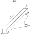
- FIG. 1 is a perspective diagram of a state where a first embodiment of the waveguide of the present invention is combined with a millimeter-wave module 300, as viewed obliquely from above.
- FIG. 2 is a perspective diagram of a state before a waveguide 100 and the millimeter-wave module 300 illustrated in FIG. 1 are combined with each other, as viewed from obliquely from above.
- the millimeter-wave module 300 is, for example, provided in a display panel of a liquid crystal display television (not illustrated), and is configured of a transmitting-side module 310 having a millimeter-wave antenna 311, and a receiving-side module 320 having a millimeter-wave antenna 321.
- the waveguide 100 is a waveguide for millimeter waves which is used for millimeter wave communication of 60 GHz, and links the millimeter-wave antenna 311 of the transmitting-side module 310 and the millimeter-wave antenna 321 of the receiving-side module 320.
- this waveguide 100 extends in an arrow-A direction which is a longitudinal direction, and a cross section is shaped like a rectangle.
- the display panel of the liquid crystal display television which is an object to be provided with the millimeter-wave module 300 is merely an example, and the object may be, for example, a personal computer, a gaming machine, a video recorder, a digital camera, an access point, or the like.
- FIG. 3 is an exploded perspective view of the waveguide 100 illustrated in FIG. 1 and FIG. 2 , in a state in which a main body 110 and a cover 120 are separated from each other, as viewed from obliquely above.
- FIG. 4 is a longitudinal sectional diagram taken along lines 4-4 illustrated in FIG. 3 . It is to be noted that a longitudinal sectional diagram of the main body 110 taken along the line 4-4 illustrated in FIG. 3 and a longitudinal sectional diagram of the cover 120 taken along the line 4-4 illustrated in FIG. 3 are similar and thus, FIG. 4 illustrates only the longitudinal sectional diagram of one of them as representing both.
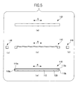
- FIG. 5 is a diagram illustrating appearances of the main body 110 illustrated in FIG. 3 , and FIG.
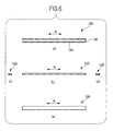
- FIG. 6 is a diagram illustrating appearances of the cover 120 illustrated in FIG. 3 .
- (a) is a plan view
- (b) is a front view
- (c) is a left-side view
- (d) is a right-side view
- (e) is a bottom view.
- the waveguide 100 is a hollow waveguide made of resin, and configured of the main body 110 and the cover 120, and has a metal plating layer 130 on an inner surface of a tube made of resin (namely, an inner wall of a transmission path).
- the main body 110 illustrated in FIG. 3 to FIG. 5 is formed by two-color molding of an ABS resin to form an internal layer 111 by adhering to the metal plating layer 130, and a polycarbonate resin to form an external layer 112 by adhering to the ABS resin without adhering to the metal plating layer 130.
- This ABS resin is an example of the first resin according to the present invention
- this polycarbonate resin is an example of the second resin according to the present invention.
- the main body 110 there is formed a concave groove 113 formed in an inner part excluding both end portions 110a and 110b of the main body 110 in the arrow-A direction and inside these both end portions 110a and 110b, and extending in the arrow-A direction.
- the main body 110 has the metal plating layer 130 over the entire surface of the concave groove 113.
- the cover 120 illustrated in FIG. 3 , FIG. 4 and FIG. 6 is formed by two-color molding of an ABS resin to form an internal layer 121 by adhering to the metal plating layer 130, and a polycarbonate resin to form an external layer 122 by adhering to the ABS resin without adhering to the metal plating layer 130.
- This ABS resin is an example of the first resin according to the present invention
- this polycarbonate resin is an example of the second resin according to the present invention.
- the cover 120 covers a part excluding both end portions 113a and 113b in the arrow-A direction of the concave groove 113 of the main body 110, the part being inner than the both end portions 113a and 113b of the concave groove 113 of the main body 110.
- this cover 120 is formed a concave groove 123 having a width equal to a width of the concave groove 113 of the main body 110 and extending in the arrow-A direction.
- the cover 120 has the metal plating layer 130 at a part of an inner wall that defines a hollow inner space (a transmission path) formed by covering the concave groove 113 of the main body 110 with the cover 120 and bonding them, namely, over the entire surface of the concave groove 123 of the cover 120.
- the metal plating layer 130 has a two-layer structure considering protection against corrosion. Specifically, this metal plating layer 130 has: a copper plating layer 131 adhering to the ABS resin forming each of the internal layers 111 and 121 of the main body 110 and the cover 120; and a nickel plating layer 132 adhering to and laminated on this copper plating layer 131. Further, the surface of the ABS resin adhering to the metal plating layer 130 and forming the internal layers 111 and 121 is roughened in order to increase a degree of adherence to the plating.
- the waveguide 100 What is formed by covering the concave groove 113 of the main body 110 with the cover 120 and bonding them is the waveguide 100, and the hollow inner space formed by this becomes the transmission path. Further, the concave groove 113 of the main body 110 is formed inside the both end portions 110a and 110b of the main body 110, and the cover 120 covers the part inner than the both end portions 113a and 113b of the concave groove 113, and thereby, this waveguide 100 has the transmission path shaped like a letter U as a whole.
- the cross section of this transmission path has a rectangular shape, and the waveguide 100 is a waveguide for millimeter waves used for millimeter wave communication of 60 GHz and therefore, the section size of this transmission path is, for example, "0.4 mm ⁇ 0.4 mm.” It is to be noted that the section size of the transmission path may be larger than or smaller than "0.4 mm ⁇ 0.4 mm.”
- the waveguide 100 of the first embodiment is configured of the main body 110 and the cover 120, and the transmission path is the hollow inner space formed by the respective concave grooves 113 and 123 of the main body 110 and the cover 120. Therefore, when the metal plating layer 130 is formed on each of the main body 110 and the cover 120, a state in which the main body 110 and the cover 120 are separate from each other, namely, a state in which an area where the metal plating layer 130 is to be formed is exposed may be established.
- the waveguide 100 of the first embodiment even if the section size of the transmission path in which the cross section has the rectangular shape is "0.4 mm ⁇ 0.4 mm" which is extremely small, it is possible to avoid a problem of clogging of the transmission path due to plating accumulation. Further, according to the waveguide 100 of the first embodiment, it is possible to avoid such a problem that the greater the length of the waveguide in the arrow-A direction which is the longitudinal direction of the waveguide is, the higher the probability of occurrence of plating unevenness becomes. Moreover, according to the waveguide 100 of the first embodiment, visual checking of the state of the metal plating layer 130 is easy and thus, a defect of the metal plating layer such as "plating missing" may be removed. As a result, the surface of the metal plating layer 130 may be made even.
- FIG. 7 is an exploded perspective view of the second embodiment of the waveguide of the present invention, in a state in which a main body 210 and a cover 220 are separated from each other, as viewed obliquely from above.
- FIG. 8 is a longitudinal sectional diagram taken along a line 8-8 illustrated in FIG. 7
- FIG. 9 is a longitudinal sectional diagram taken along a line 9-9 illustrated in FIG. 7 .
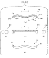
- FIG. 10 is a diagram illustrating appearances of the main body 210 illustrated in FIG. 7
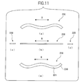
- FIG. 11 is a diagram illustrating appearances of the cover 220 illustrated in FIG. 7 .
- (a) is a plan view
- (b) is a front view
- (c) is a left-side view
- (d) is a right-side view
- (e) is a bottom view.
- a waveguide 200 is a hollow waveguide made of resin and is configured of the main body 210 and the cover 220, and has a metal plating layer 230 on an inner surface of a tube made of resin (namely, an inner wall of a transmission path) . Further, this waveguide 200 extends in an arrow-B direction which is a longitudinal direction while curving, and has a rectangular cross section. Furthermore, like the waveguide 100 of the first embodiment, this waveguide 200 is a waveguide for millimeter waves used for millimeter wave communication of 60 GHz.
- the main body 210 illustrated in FIG. 7 , FIG. 8 and FIG. 10 is formed by molding an ABS resin.
- This ABS resin is an example of the resin member according to the present invention.
- a concave groove 211 that is formed in a part excluding both end portions 210a and 210b of the main body 210 in the arrow-B direction, the part being inside the both end portions 210a and 210b, and extends in the arrow-B direction.
- the main body 210 has the metal plating layer 230 over the entire surface of the concave groove 211.
- the main body 210 has, at each of both end portions 211a and 211b of the concave groove 211 in the arrow-B direction, a through hole 212 that penetrates the main body 210 in an arrow-C direction that is a direction intersecting the arrow-B direction and has the metal plating layer 230 over the entire surface.
- this concave groove 211 and the through hole 212 may be formed by molding, or may be formed by, for example, cutting.
- the cover 220 illustrated in FIG. 7 , FIG. 9 and FIG. 11 is formed by molding an ABS resin. Further, the cover 220 has a flat shape having a width equal to a width of the main body 210, and covers the entire concave groove 211 of the main body 210. Furthermore, the cover 220 has the metal plating layer 230 over an entire face 221 including a part of an inner wall that defines a hollow inner space (a transmission path) formed by covering the concave groove 211 of the main body 210 with the cover 220 and applying ultrasonic welding or heat welding thereto.
- the metal plating layer 230 has a three-layer structure considering protection against corrosion. Specifically, this metal plating layer 230 has a copper plating layer 231 adhering to the ABS resin forming each of the main body 210 and the cover 220, a nickel plating layer 232 adhering to and laminated on this copper plating layer 231, and a gold plating layer 233 adhering to and laminated on this nickel plating layer 232.
- the metal plating layer 230 which is formed by plating the surface of the ABS resin forming each of the main body 210 and the cover 220 with metal after selectively roughening the surfaces, is obtained by masking an area of the surface of the ABS resin excluding the above-described plating area, in a roughening process and a plating process.
- the waveguide 200 What is formed by covering the concave groove 211 of the main body 210 with the cover 220 and applying ultrasonic welding or heat welding thereto is the waveguide 200, and the hollow inner space formed thereby becomes the transmission path.
- the concave groove 211 of the main body 210 is formed inside the both end portions 210a and 210b of the main body 210 and furthermore, the through hole 212 is provided in each of the both end portions 211a and 211b of the concave groove 211, and the cover 220 covers the entire concave groove 211 and thereby, this waveguide 200 has the transmission path shaped like a letter U in a manner similar to the waveguide 100 of the first embodiment.
- the cross section of this transmission path is rectangular, and the waveguide 100 is the waveguide for millimeter waves used for the millimeter wave communication of 60 GHz and thus, the section size of this transmission path is, for example, "0.4 mm ⁇ 0.4 mm.” It is to be noted that the section size of the transmission path may be larger than, or may be smaller than "0.4 mm ⁇ 0.4 mm.”
- the waveguide 200 of the second embodiment has been described by taking the example in which "each of the main body and the cover is made of one kind of resin having the metal plating layer selectively, and the selective metal plating layer is obtained by masking the area excluding the plating area in the roughening process and the plating process.”
- the way of implementing the selective metal plating layer on the waveguide having the one kind of resin is not limited to this.
- it may be a way of implementing a selective metal plating layer, in which "each of a main body and a cover is made of one kind of resin with copper mixed, and the copper is separated from the resin by irradiating a selected area of the surface of this resin with an infrared laser and exposed at a laser irradiation point, and this is put in a copper plating bath, so that a copper plating layer is selectively formed.”
- the waveguide 200 of the second embodiment is configured of the main body 210 and the cover 220, and the transmission path is the hollow inner space formed by covering the concave groove 211 of the main body 210 with the cover 220 having a flat shape.
- the metal plating layer 230 is formed at each of the main body 210 and the cover 220, in a manner similar to that of the waveguide 100 of the first embodiment, a state in which the main body 210 and the cover 220 are separate from each other, namely, a state in which the area where the metal plating layer 230 should be formed is exposed, may be established.
- the waveguide 200 of the second embodiment similarly to the waveguide 100 of the first embodiment, it is possible to avoid such a problem of clogging of the transmission path due to plating accumulation and such a problem that the greater the length of the waveguide in the arrow-B direction which is the longitudinal direction of the waveguide is, the higher the probability of occurrence of plating unevenness is, or eliminate a defect of the metal plating layer such as "plating missing" by visual checking, so that the surface of the metal plating layer 230 may be made even.
- the concave groove 211 is formed only in the main body 210, of the main body 210 and the cover 220 forming the waveguide 200, and the cover 220 has the flat shape and thus, production thereof is easier than that of the waveguide 100 of the first embodiment in which the concave groove is formed in each of both the main body and the cover.
- the waveguides 100 and 200 of the first embodiment and the second embodiment there is provided the waveguide made of resin, which enables the even metal plating layer to be formed irrespective of the length in the longitudinal length and the diameter of the transmission path, and makes checking of the formed metal plating easy.
- the waveguide of the present invention may support various shapes, such as a shape extending linearly in a longitudinal direction like the waveguide 100 of the first embodiment and a shape extending in a longitudinal direction while curving like the waveguide 200 of the second embodiment.
- the waveguide of the present invention is the millimeter-wave waveguide used for the millimeter wave communication of 60 GHz, but the waveguide of the present invention is not limited to these, and may be, for example, a millimeter-wave waveguide used for microwave communication, or may be a millimeter-wave antenna.
- each of the main body 210 and the cover 220 of the waveguide 200 may be formed by two-color molding.
- each of the main body and the cover according to the present invention is one piece in the longitudinal direction, but each of the main body and the cover according to the present invention is not limited thereto and may be formed by integrating segments resulting from division in a longitudinal direction.
Landscapes
- Engineering & Computer Science (AREA)
- Manufacturing & Machinery (AREA)
- Waveguides (AREA)
Abstract
The present invention relates to a waveguide formed by plating an inner surface of a tube made of resin with metal, and aims to provide a waveguide made of resin, in which an even metal plating layer may be formed irrespective of a length in a longitudinal direction and a diameter of a transmission path, and checking of the formed metal plating layer is easy. The waveguide is configured of a main body 110 and a cover 120 each made of a resin member, and has a metal plating layer 130 on both the entire surface of a concave groove of the main body 110 and a part of the cover 120, the part being of an inner wall defining a hollow inner space.
Description
- The present invention relates to a waveguide formed by plating an internal surface of a tube made of resin with metal.
- Conventionally, as a waveguide used when transmitting radio waves such as microwaves and millimeter waves, there have been known a resin waveguide made of a metal tube and a resin waveguide formed by plating an internal surface of a tube made of resin with metal.
- The transmission of radio waves by the waveguide has advantages in that transmission losses are less than those in transmission of radio waves by a wire such as a shielding wire, and a transmission loss does not increase depending on a transmission distance, and moreover, there is no influence by external electrical noise.
- Also, as the resin waveguide, for example, a resin waveguide that has a polycarbonate resin as a covering layer, an ABS resin as an adherent layer (internal layer), and a metal plating on an inner surface of the adherent layer (internal layer) has been proposed (for example, see PTL 1).
- PTL 1: Japanese Patent Application Publication No.
2003-23308 - The metal waveguide, waveguides in various shapes may be obtained by, for example, bending, but because it is made of metal, a weight reduction of a device in which the waveguide is incorporated is hindered, and a short circuit due to contact with other electrical components is likely to occur.
- In contrast, the resin waveguide proposed in the above-mentioned
PTL 1 is made of resin and thus contributes to a weight reduction of a device in which the waveguide is incorporated, and a short circuit due to contact with other electrical components is unlikely to occur. - However, the resin waveguide proposed in this
PTL 1 is generally formed by molding with a molding die, and formed by pulling the molding die along a longitudinal direction and thus, the shape of the resin waveguide is limited to a linear shape that can be pulled from the molding die. Therefore, a waveguide that needs to have a U-shaped transmission path as a whole such as a waveguide in which both a transmitting section and a receiving section face in a same direction may not be formed by the technique proposed inPTL 1. - Here, in a millimeter-wave waveguide used when transmitting millimeter waves, the diameter of a transmission path needs to be made small. In a case where the technique suggested in
PTL 1 is applied to the millimeter-wave waveguide of such a small diameter, there may occur a problem of clogging of the transmission path due to plating accumulation, when an inner surface of a resin tube (namely, an inner wall of the transmission path) is subjected to metal plating. - Also, as for the waveguide made of resin proposed in
PTL 1, in a plating process in which the inner surface of the tube made of resin is subjected to the metal plating, the greater the length of the waveguide in the longitudinal direction is, the higher the probability of occurrence of plating unevenness becomes, and it is difficult to form an even metal plating layer in the waveguide made of resin that is long in the longitudinal direction. - Further, in the waveguide made of resin proposed in
PTL 1, a part where the metal plating layer is formed is the inner surface of the waveguide made of resin and thus, the state of the metal plating layer after being formed may not be visually checked. Therefore, even when, for example, a defect such as a so-called "plating missing" in which plating does not adhere to a resin in a plating process occurs, this defect may be overlooked. - In view of the foregoing circumstances, it is an object of the present invention to provide a waveguide made of resin in which an even metal plating layer may be formed irrespective of the length in a longitudinal direction and the diameter of a transmission path, and the formed metal plating layer may be easily checked.
- A waveguide to achieve the object includes:
- a main body in which a concave groove extending in a longitudinal direction is formed, which has a metal plating layer over an entire surface of the concave groove, and which is made of a resin member; and
- a cover which covers the concave groove of the main body, which has a metal plating layer at a part of an inner wall defining a hollow inner space formed by covering the concave groove, and which is made of a resin member.
- The waveguide of the present invention is configured of the main body and the cover each made of a resin member, and has the metal plating layer on both the entire surface of the concave groove of the main body and the part of the cover, the part of the inner wall defining the hollow inner space. Therefore, when the metal plating layer is formed on each of the main body and the cover, a state in which the main body and the cover are separate from each other, namely, a state in which an area where the metal plating layer is to be formed is exposed may be obtained. Thus, according to the waveguide of the present invention, even if the diameter of the transmission path is extremely small, it is possible to avoid a problem of clogging of the transmission path due to plating accumulation. Further, according to the waveguide of the present invention, it is possible to avoid such a problem that the greater the length of the waveguide in the longitudinal direction is, the higher the probability of occurrence of plating unevenness is. Furthermore, according to the waveguide of the present invention, the state of the metal plating layer may be easily checked with eyes and thus, it is also possible to eliminate a defect of the metal plating layer such as "plating missing." As a result, in waveguides of various shapes including not only a waveguide in a shape extending linearly in a longitudinal direction, but also a waveguide in, for example, a shape extending in a longitudinal direction while curving, it is possible to make the surface of a metal plating layer even.
- Here, in the waveguide according to the present invention, it is preferable that the resin member is formed by two-color molding of a first resin forming an internal layer by adhering to the metal plating layer, and a second resin forming an external layer by adhering to the first resin without adhering to the metal plating layer.
- According to such a preferable form, it is possible to reliably form the metal plating layer in the area, in which the metal plating layer is to be formed, of the main body and the cover.
- Further, in the waveguide according to the present invention, it is also preferable that the cover has a flat shape, and has the metal plating layer over an entire face including the part of the inner wall defining the hollow inner space formed by covering the concave groove of the main body.
- According to such a preferable form, production of the cover is easy.
- Furthermore, in the waveguide according to the present invention, it is preferable that "the concave groove of the main body is formed at a part excluding both end portions of the main body in the longitudinal direction, the part being inside the both end portions, and
the cover covers a part excluding both end portions of the concave groove in the longitudinal direction, the part being inner than the both end portions of the concave groove", and it is also preferable that "the concave groove of the main body is formed at a part excluding both end portions of the main body in the longitudinal direction, the part being inside the both end portions, and
the main body has a through hole passing through the main body in a direction intersecting the longitudinal direction, at each of both end portions of the concave groove in the longitudinal direction, the through hole having the metal plating layer over an entire surface, and the cover covers the entire concave groove." - According to these preferable forms, it is possible to obtain a waveguide in which both a transmitting section and a receiving section face in the same direction, and which has a transmission path shaped like a letter U as a whole.
- According to the present invention, there is provided a waveguide made of resin which may support various shapes, in which an even metal plating layer may be formed irrespective of the length in a longitudinal length and the diameter of a transmission path, and in which the formed metal plating layer is readily checked.
-
-
FIG. 1 is a perspective diagram of a state where a first embodiment of a waveguide of the present invention is combined with a millimeter-wave module, as viewed obliquely from above. -
FIG. 2 is a perspective diagram of a state before a waveguide and the millimeter-wave module illustrated inFIG. 1 are combined with each other, as viewed from obliquely from above. -
FIG. 3 is an exploded perspective view of the waveguide illustrated inFIG. 1 andFIG. 2 , in a state in which a main body and a cover are separated from each other, as viewed from obliquely above. -
FIG. 4 is a longitudinal sectional diagram taken along lines 4-4 illustrated inFIG. 3 . -
FIG. 5 is a diagram illustrating appearances of the main body illustrated inFIG. 3 . -
FIG. 6 is a diagram illustrating appearances of the cover illustrated inFIG. 3 . -
FIG. 7 is an exploded perspective view of the second embodiment of the waveguide of the present invention, in a state in which a main body and a cover are separated from each other, as viewed obliquely from above. -
FIG. 8 is a longitudinal sectional diagram taken along a line 8-8 illustrated inFIG. 7 . -
FIG. 9 is a longitudinal sectional diagram taken along a line 9-9 illustrated inFIG. 7 . -
FIG. 10 is a diagram illustrating appearances of the main body illustrated inFIG. 7 . -
FIG. 11 is a diagram illustrating appearances of the cover illustrated inFIG. 7 . - Embodiments of the present invention will be described with reference to the drawings.
-
FIG. 1 is a perspective diagram of a state where a first embodiment of the waveguide of the present invention is combined with a millimeter-wave module 300, as viewed obliquely from above.FIG. 2 is a perspective diagram of a state before awaveguide 100 and the millimeter-wave module 300 illustrated inFIG. 1 are combined with each other, as viewed from obliquely from above. - As illustrated in
FIG. 1 andFIG. 2 , the millimeter-wave module 300 is, for example, provided in a display panel of a liquid crystal display television (not illustrated), and is configured of a transmitting-side module 310 having a millimeter-wave antenna 311, and a receiving-side module 320 having a millimeter-wave antenna 321. And, thewaveguide 100 is a waveguide for millimeter waves which is used for millimeter wave communication of 60 GHz, and links the millimeter-wave antenna 311 of the transmitting-side module 310 and the millimeter-wave antenna 321 of the receiving-side module 320. Also, thiswaveguide 100 extends in an arrow-A direction which is a longitudinal direction, and a cross section is shaped like a rectangle. - It is to be noted that the display panel of the liquid crystal display television which is an object to be provided with the millimeter-
wave module 300 is merely an example, and the object may be, for example, a personal computer, a gaming machine, a video recorder, a digital camera, an access point, or the like. -
FIG. 3 is an exploded perspective view of thewaveguide 100 illustrated inFIG. 1 andFIG. 2 , in a state in which amain body 110 and acover 120 are separated from each other, as viewed from obliquely above. Further,FIG. 4 is a longitudinal sectional diagram taken along lines 4-4 illustrated inFIG. 3 . It is to be noted that a longitudinal sectional diagram of themain body 110 taken along the line 4-4 illustrated inFIG. 3 and a longitudinal sectional diagram of thecover 120 taken along the line 4-4 illustrated inFIG. 3 are similar and thus,FIG. 4 illustrates only the longitudinal sectional diagram of one of them as representing both. Further,FIG. 5 is a diagram illustrating appearances of themain body 110 illustrated inFIG. 3 , andFIG. 6 is a diagram illustrating appearances of thecover 120 illustrated inFIG. 3 . InFIG. 5 andFIG. 6 , (a) is a plan view, (b) is a front view, (c) is a left-side view, (d) is a right-side view, and (e) is a bottom view. - As illustrated in
FIG. 3 , thewaveguide 100 is a hollow waveguide made of resin, and configured of themain body 110 and thecover 120, and has ametal plating layer 130 on an inner surface of a tube made of resin (namely, an inner wall of a transmission path). - The
main body 110 illustrated inFIG. 3 to FIG. 5 is formed by two-color molding of an ABS resin to form aninternal layer 111 by adhering to themetal plating layer 130, and a polycarbonate resin to form anexternal layer 112 by adhering to the ABS resin without adhering to themetal plating layer 130. This ABS resin is an example of the first resin according to the present invention, and this polycarbonate resin is an example of the second resin according to the present invention. Further, in themain body 110, there is formed aconcave groove 113 formed in an inner part excluding bothend portions main body 110 in the arrow-A direction and inside these bothend portions main body 110 has themetal plating layer 130 over the entire surface of theconcave groove 113. - Similarly to the
main body 110, thecover 120 illustrated inFIG. 3 ,FIG. 4 andFIG. 6 is formed by two-color molding of an ABS resin to form aninternal layer 121 by adhering to themetal plating layer 130, and a polycarbonate resin to form anexternal layer 122 by adhering to the ABS resin without adhering to themetal plating layer 130. This ABS resin is an example of the first resin according to the present invention, and this polycarbonate resin is an example of the second resin according to the present invention. Further, thecover 120 covers a part excluding bothend portions concave groove 113 of themain body 110, the part being inner than the bothend portions concave groove 113 of themain body 110. In thiscover 120 is formed aconcave groove 123 having a width equal to a width of theconcave groove 113 of themain body 110 and extending in the arrow-A direction. Furthermore, thecover 120 has themetal plating layer 130 at a part of an inner wall that defines a hollow inner space (a transmission path) formed by covering theconcave groove 113 of themain body 110 with thecover 120 and bonding them, namely, over the entire surface of theconcave groove 123 of thecover 120. - As illustrated in
FIG. 4 , in the present embodiment, themetal plating layer 130 has a two-layer structure considering protection against corrosion. Specifically, thismetal plating layer 130 has: acopper plating layer 131 adhering to the ABS resin forming each of theinternal layers main body 110 and thecover 120; and anickel plating layer 132 adhering to and laminated on thiscopper plating layer 131. Further, the surface of the ABS resin adhering to themetal plating layer 130 and forming theinternal layers - What is formed by covering the
concave groove 113 of themain body 110 with thecover 120 and bonding them is thewaveguide 100, and the hollow inner space formed by this becomes the transmission path. Further, theconcave groove 113 of themain body 110 is formed inside the bothend portions main body 110, and thecover 120 covers the part inner than the bothend portions concave groove 113, and thereby, thiswaveguide 100 has the transmission path shaped like a letter U as a whole. The cross section of this transmission path has a rectangular shape, and thewaveguide 100 is a waveguide for millimeter waves used for millimeter wave communication of 60 GHz and therefore, the section size of this transmission path is, for example, "0.4 mm × 0.4 mm." It is to be noted that the section size of the transmission path may be larger than or smaller than "0.4 mm × 0.4 mm." - In this way, the
waveguide 100 of the first embodiment is configured of themain body 110 and thecover 120, and the transmission path is the hollow inner space formed by the respectiveconcave grooves main body 110 and thecover 120. Therefore, when themetal plating layer 130 is formed on each of themain body 110 and thecover 120, a state in which themain body 110 and thecover 120 are separate from each other, namely, a state in which an area where themetal plating layer 130 is to be formed is exposed may be established. Thus, according to thewaveguide 100 of the first embodiment, even if the section size of the transmission path in which the cross section has the rectangular shape is "0.4 mm × 0.4 mm" which is extremely small, it is possible to avoid a problem of clogging of the transmission path due to plating accumulation. Further, according to thewaveguide 100 of the first embodiment, it is possible to avoid such a problem that the greater the length of the waveguide in the arrow-A direction which is the longitudinal direction of the waveguide is, the higher the probability of occurrence of plating unevenness becomes. Moreover, according to thewaveguide 100 of the first embodiment, visual checking of the state of themetal plating layer 130 is easy and thus, a defect of the metal plating layer such as "plating missing" may be removed. As a result, the surface of themetal plating layer 130 may be made even. - This concludes the description of the first embodiment of the present invention, and a second embodiment of the present invention will be described.
-
FIG. 7 is an exploded perspective view of the second embodiment of the waveguide of the present invention, in a state in which amain body 210 and acover 220 are separated from each other, as viewed obliquely from above. Further,FIG. 8 is a longitudinal sectional diagram taken along a line 8-8 illustrated inFIG. 7 , andFIG. 9 is a longitudinal sectional diagram taken along a line 9-9 illustrated inFIG. 7 . Furthermore,FIG. 10 is a diagram illustrating appearances of themain body 210 illustrated inFIG. 7 , andFIG. 11 is a diagram illustrating appearances of thecover 220 illustrated inFIG. 7 . InFIG. 10 andFIG. 11 , (a) is a plan view, (b) is a front view, (c) is a left-side view, (d) is a right-side view, and (e) is a bottom view. - As illustrated in
FIG. 7 , awaveguide 200 is a hollow waveguide made of resin and is configured of themain body 210 and thecover 220, and has ametal plating layer 230 on an inner surface of a tube made of resin (namely, an inner wall of a transmission path) . Further, thiswaveguide 200 extends in an arrow-B direction which is a longitudinal direction while curving, and has a rectangular cross section. Furthermore, like thewaveguide 100 of the first embodiment, thiswaveguide 200 is a waveguide for millimeter waves used for millimeter wave communication of 60 GHz. - The
main body 210 illustrated inFIG. 7 ,FIG. 8 andFIG. 10 is formed by molding an ABS resin. This ABS resin is an example of the resin member according to the present invention. Further, in themain body 210, there is formed aconcave groove 211 that is formed in a part excluding bothend portions main body 210 in the arrow-B direction, the part being inside the bothend portions main body 210 has themetal plating layer 230 over the entire surface of theconcave groove 211. Moreover, themain body 210 has, at each of bothend portions concave groove 211 in the arrow-B direction, a throughhole 212 that penetrates themain body 210 in an arrow-C direction that is a direction intersecting the arrow-B direction and has themetal plating layer 230 over the entire surface. It is to be noted that thisconcave groove 211 and the throughhole 212 may be formed by molding, or may be formed by, for example, cutting. - Similarly to the
main body 210, thecover 220 illustrated inFIG. 7 ,FIG. 9 andFIG. 11 is formed by molding an ABS resin. Further, thecover 220 has a flat shape having a width equal to a width of themain body 210, and covers the entireconcave groove 211 of themain body 210. Furthermore, thecover 220 has themetal plating layer 230 over anentire face 221 including a part of an inner wall that defines a hollow inner space (a transmission path) formed by covering theconcave groove 211 of themain body 210 with thecover 220 and applying ultrasonic welding or heat welding thereto. - As illustrated in
FIG. 8 and FIG. 9 , in the present embodiment, themetal plating layer 230 has a three-layer structure considering protection against corrosion. Specifically, thismetal plating layer 230 has acopper plating layer 231 adhering to the ABS resin forming each of themain body 210 and thecover 220, anickel plating layer 232 adhering to and laminated on thiscopper plating layer 231, and agold plating layer 233 adhering to and laminated on thisnickel plating layer 232. Further, among the surfaces of the ABS resin forming each of themain body 210 and thecover 220, a surface of each of theconcave groove 211 and the throughhole 212 of themain body 210 as well as theface 221 of thecover 220, each of which is an area adhering to the metal plating layer 230 (this area will be hereinafter referred to as a plating area), are roughened to increase a degree of adherence to the plating. Thus, themetal plating layer 230, which is formed by plating the surface of the ABS resin forming each of themain body 210 and thecover 220 with metal after selectively roughening the surfaces, is obtained by masking an area of the surface of the ABS resin excluding the above-described plating area, in a roughening process and a plating process. - What is formed by covering the
concave groove 211 of themain body 210 with thecover 220 and applying ultrasonic welding or heat welding thereto is thewaveguide 200, and the hollow inner space formed thereby becomes the transmission path. Further, theconcave groove 211 of themain body 210 is formed inside the bothend portions main body 210 and furthermore, the throughhole 212 is provided in each of the bothend portions concave groove 211, and thecover 220 covers the entireconcave groove 211 and thereby, thiswaveguide 200 has the transmission path shaped like a letter U in a manner similar to thewaveguide 100 of the first embodiment. Moreover, similarly to thewaveguide 100 of the first embodiment, the cross section of this transmission path is rectangular, and thewaveguide 100 is the waveguide for millimeter waves used for the millimeter wave communication of 60 GHz and thus, the section size of this transmission path is, for example, "0.4 mm × 0.4 mm." It is to be noted that the section size of the transmission path may be larger than, or may be smaller than "0.4 mm × 0.4 mm." - It is to be noted that the
waveguide 200 of the second embodiment has been described by taking the example in which "each of the main body and the cover is made of one kind of resin having the metal plating layer selectively, and the selective metal plating layer is obtained by masking the area excluding the plating area in the roughening process and the plating process." However, the way of implementing the selective metal plating layer on the waveguide having the one kind of resin is not limited to this. For example, it may be a way of implementing a selective metal plating layer, in which "each of a main body and a cover is made of one kind of resin with copper mixed, and the copper is separated from the resin by irradiating a selected area of the surface of this resin with an infrared laser and exposed at a laser irradiation point, and this is put in a copper plating bath, so that a copper plating layer is selectively formed." - In this way, the
waveguide 200 of the second embodiment is configured of themain body 210 and thecover 220, and the transmission path is the hollow inner space formed by covering theconcave groove 211 of themain body 210 with thecover 220 having a flat shape. Thus, when themetal plating layer 230 is formed at each of themain body 210 and thecover 220, in a manner similar to that of thewaveguide 100 of the first embodiment, a state in which themain body 210 and thecover 220 are separate from each other, namely, a state in which the area where themetal plating layer 230 should be formed is exposed, may be established. Therefore, according to thewaveguide 200 of the second embodiment, similarly to thewaveguide 100 of the first embodiment, it is possible to avoid such a problem of clogging of the transmission path due to plating accumulation and such a problem that the greater the length of the waveguide in the arrow-B direction which is the longitudinal direction of the waveguide is, the higher the probability of occurrence of plating unevenness is, or eliminate a defect of the metal plating layer such as "plating missing" by visual checking, so that the surface of themetal plating layer 230 may be made even. - Further, in the
waveguide 200 of the second embodiment, theconcave groove 211 is formed only in themain body 210, of themain body 210 and thecover 220 forming thewaveguide 200, and thecover 220 has the flat shape and thus, production thereof is easier than that of thewaveguide 100 of the first embodiment in which the concave groove is formed in each of both the main body and the cover. - This completes the description of the second embodiment of the present invention.
- As described above, according to the
waveguides - Further, the waveguide of the present invention may support various shapes, such as a shape extending linearly in a longitudinal direction like the
waveguide 100 of the first embodiment and a shape extending in a longitudinal direction while curving like thewaveguide 200 of the second embodiment. - It is to be noted that for each of the embodiments described above, the description has been provided by taking the example in which the waveguide of the present invention is the millimeter-wave waveguide used for the millimeter wave communication of 60 GHz, but the waveguide of the present invention is not limited to these, and may be, for example, a millimeter-wave waveguide used for microwave communication, or may be a millimeter-wave antenna.
- Furthermore, for each of the embodiments described above, the description has been provided by taking the example in which the metal plating layer according to the present invention has the two-layer structure or the three-layer structure, but the metal plating layer according to the present invention is not limited to these, and may be a metal plating layer having at least one layer in a case where protection against corrosion is not considered.
- Moreover, each of the
main body 210 and thecover 220 of thewaveguide 200 may be formed by two-color molding. - Also, for each of the embodiments described above, the description has been provided by taking the example in which the waveguide of the present invention has the rectangular cross section, but the waveguide of the present invention is not limited to these, and may have, for example, a circular cross section.
- Further, for each of the embodiments described above, the description has been provided by taking the example in which the hollow inner space (transmission path) is defined by bonding the main body and the cover of the present invention to each other or applying the ultrasonic welding or the heat welding thereto, but these are not limitations, and, for example, the hollow inner space (transmission path) may be defined by fitting or the like.
- Furthermore, for each of the embodiments described above, the description has been provided by taking the example in which each of the main body and the cover according to the present invention is one piece in the longitudinal direction, but each of the main body and the cover according to the present invention is not limited thereto and may be formed by integrating segments resulting from division in a longitudinal direction.
-
- 100, 200:
- Waveguide
- 110, 210:
- Main body
- 110a, 110b, 113a, 113b, 210a, 210b, 211a, 211b:
- Both end portions
- 111, 121:
- Internal layer
- 112, 122:
- External layer
- 113, 123, 211:
- Concave groove
- 212: Through
- hole
- 120, 220:
- Cover
- 221:
- Face
- 130, 230:
- Metal plating layer
- 131, 231:
- Copper plating layer
- 132, 232:
- Nickel plating layer
- 233:
- Gold plating layer
- 300:
- Millimeter-wave module
- 310:
- Transmitting-side module
- 311:
- Millimeter-wave antenna
- 320:
- Receiving-side module
- 321:
- Millimeter-wave antenna
Claims (6)
- A waveguide comprising:a main body in which a concave groove extending in a longitudinal direction is formed, which has a metal plating layer over an entire surface of the concave groove, and which is made of a resin member; anda cover which covers the concave groove of the main body, which has a metal plating layer at a part of an inner wall defining a hollow inner space formed by covering the concave groove, and which is made of a resin member.
- The waveguide according to claim 1, wherein the resin member is formed by two-color molding of a first resin forming an internal layer by adhering to the metal plating layer, and a second resin forming an external layer by adhering to the first resin without adhering to the metal plating layer.
- The waveguide according to claim 1, wherein the cover has a flat shape, and has the metal plating layer over an entire face including the part of the inner wall defining the hollow inner space formed by covering the concave groove of the main body.
- The waveguide according to claim 2, wherein the cover has a flat shape, and has the metal plating layer over an entire face including the part of the inner wall defining the hollow inner space formed by covering the concave groove of the main body.
- The waveguide according to any of claims 1 to 4, wherein the concave groove of the main body is formed at a part excluding both end portions of the main body in the longitudinal direction, the part being inside the both end portions, and
the cover covers a part excluding both end portions of the concave groove in the longitudinal direction, the part being inner than the both end portions of the concave groove. - The waveguide according to any of claims 1 to 4, wherein the concave groove of the main body is formed at a part excluding both end portions of the main body in the longitudinal direction, the part being inside the both end portions, and
the main body has a through hole passing through the main body in a direction intersecting the longitudinal direction, at each of both end portions of the concave groove in the longitudinal direction, the through hole having the metal plating layer over an entire surface, and
the cover covers the entire concave groove.
Applications Claiming Priority (2)
| Application Number | Priority Date | Filing Date | Title |
|---|---|---|---|
| JP2009099970A JP2010252092A (en) | 2009-04-16 | 2009-04-16 | Waveguide |
| PCT/JP2010/055905 WO2010119776A1 (en) | 2009-04-16 | 2010-03-31 | Waveguide |
Publications (1)
| Publication Number | Publication Date |
|---|---|
| EP2421086A1 true EP2421086A1 (en) | 2012-02-22 |
Family
ID=42982438
Family Applications (1)
| Application Number | Title | Priority Date | Filing Date |
|---|---|---|---|
| EP10764361A Withdrawn EP2421086A1 (en) | 2009-04-16 | 2010-03-31 | Waveguide |
Country Status (7)
| Country | Link |
|---|---|
| US (1) | US20120033931A1 (en) |
| EP (1) | EP2421086A1 (en) |
| JP (1) | JP2010252092A (en) |
| KR (1) | KR101661002B1 (en) |
| CN (1) | CN102396102A (en) |
| TW (1) | TWM390554U (en) |
| WO (1) | WO2010119776A1 (en) |
Families Citing this family (12)
| Publication number | Priority date | Publication date | Assignee | Title |
|---|---|---|---|---|
| JP2013140119A (en) * | 2012-01-06 | 2013-07-18 | Hitachi-Ge Nuclear Energy Ltd | Method of monitoring reactor bottom section, apparatus for monitoring reactor bottom section, and nuclear reactor |
| WO2014106891A1 (en) * | 2013-01-04 | 2014-07-10 | 富士通株式会社 | Wireless communication devi ce and electronic device |
| JP6282266B2 (en) * | 2013-04-03 | 2018-02-21 | ソニーセミコンダクタソリューションズ株式会社 | Waveguide, waveguide manufacturing method, and wireless transmission system |
| JP6374185B2 (en) * | 2013-06-18 | 2018-08-15 | Ntn株式会社 | Waveguide slot antenna and alarm system using the same |
| KR20160108856A (en) | 2015-03-09 | 2016-09-21 | 한국전자통신연구원 | Electromagnetic wave sensor and method for generating the electromagnetic wave sensor |
| JP6256776B2 (en) * | 2015-10-15 | 2018-01-10 | 日本電産株式会社 | Waveguide device and antenna device including the waveguide device |
| US10490874B2 (en) * | 2016-03-18 | 2019-11-26 | Te Connectivity Corporation | Board to board contactless interconnect system using waveguide sections connected by conductive gaskets |
| FR3051924B1 (en) * | 2016-05-30 | 2020-04-10 | Swissto 12 Sa | WAVEGUIDE INCLUDING A THICK CONDUCTIVE LAYER |
| FR3075483B1 (en) | 2017-12-20 | 2019-12-27 | Swissto12 Sa | PASSIVE RADIO FREQUENCY DEVICE, AND MANUFACTURING METHOD |
| JP7142591B2 (en) | 2019-03-04 | 2022-09-27 | モレックス エルエルシー | waveguide |
| CN114122656B (en) * | 2020-08-31 | 2022-12-13 | 台湾禾邦电子有限公司 | Electronic device, its waveguide structure, and manufacturing method of the waveguide structure |
| CN118523059B (en) * | 2024-06-24 | 2025-05-09 | 南京驰韵科技发展有限公司 | Processing method of Ka-band space S-bend data transmission waveguide |
Family Cites Families (27)
| Publication number | Priority date | Publication date | Assignee | Title |
|---|---|---|---|---|
| JPS5126391U (en) * | 1974-08-14 | 1976-02-26 | ||
| JPS5660768U (en) * | 1979-10-15 | 1981-05-23 | ||
| JPS6429004A (en) * | 1987-07-24 | 1989-01-31 | Hitachi Ltd | Manufacture of slot array antenna |
| JPH0666538B2 (en) * | 1988-02-16 | 1994-08-24 | 三共化成株式会社 | Molded circuit parts |
| JPH0284790A (en) * | 1988-09-21 | 1990-03-26 | Hitachi Chem Co Ltd | Manufacture of molding with conductive circuit |
| CA2085131A1 (en) * | 1990-06-14 | 1991-12-15 | John L. F. C. Collins | Microwave antennas |
| JPH0483876A (en) * | 1990-07-25 | 1992-03-17 | Hitachi Cable Ltd | Plastic two-shot molded product |
| JPH0457908U (en) * | 1990-09-25 | 1992-05-19 | ||
| US5398010A (en) * | 1992-05-07 | 1995-03-14 | Hughes Aircraft Company | Molded waveguide components having electroless plated thermoplastic members |
| ES2126612T3 (en) * | 1992-05-07 | 1999-04-01 | Raytheon Co | COMPONENTS FOR MICROWAVES WITH METALLIC MOLDED PLASTIC AND MANUFACTURING PROCEDURE. |
| JPH06244611A (en) * | 1993-02-12 | 1994-09-02 | Toshiba Corp | High frequency distributor |
| JP3289603B2 (en) * | 1996-07-05 | 2002-06-10 | 日立電線株式会社 | Radiation leakage waveguide line |
| US5929728A (en) * | 1997-06-25 | 1999-07-27 | Hewlett-Packard Company | Imbedded waveguide structures for a microwave circuit package |
| JP4011240B2 (en) * | 1999-08-11 | 2007-11-21 | 株式会社Kddi研究所 | Waveguide line |
| JP2001308611A (en) * | 2000-04-25 | 2001-11-02 | Kojima Press Co Ltd | Waveguide antenna |
| JP2003023308A (en) * | 2001-07-05 | 2003-01-24 | Mitsubishi Electric Corp | Resin waveguide |
| JP2003209411A (en) * | 2001-10-30 | 2003-07-25 | Matsushita Electric Ind Co Ltd | High frequency module and method of manufacturing high frequency module |
| JP4183445B2 (en) * | 2001-11-16 | 2008-11-19 | ポリマテック株式会社 | Manufacturing method of key top for pushbutton switch |
| KR100515492B1 (en) * | 2001-12-27 | 2005-09-20 | 미쓰이 가가쿠 가부시키가이샤 | Circuit board and method of producing the same |
| JP3910880B2 (en) * | 2002-05-30 | 2007-04-25 | シャープ株式会社 | Satellite communication receiving converter feed horn, method for manufacturing the same, and satellite communication receiving converter |
| JP3744468B2 (en) * | 2002-06-07 | 2006-02-08 | 三菱電機株式会社 | Resin waveguide |
| JP3843946B2 (en) * | 2003-01-10 | 2006-11-08 | 三菱電機株式会社 | Waveguide converter |
| JP2005020077A (en) * | 2003-06-23 | 2005-01-20 | Oki Electric Ind Co Ltd | 90 degree bent waveguide, waveguide filter element, and high frequency circuit unit |
| JP3955028B2 (en) * | 2004-03-02 | 2007-08-08 | 三共化成株式会社 | Waveguide / conductive structure |
| CN2752963Y (en) * | 2004-06-30 | 2006-01-18 | 炬鑫科技股份有限公司 | Vertical Electrode Structure of White Light Emitting Diode |
| CN1797847A (en) * | 2004-12-28 | 2006-07-05 | 天迈企业股份有限公司 | Film antenna and manufacturing method thereof |
| US7680464B2 (en) * | 2004-12-30 | 2010-03-16 | Valeo Radar Systems, Inc. | Waveguide—printed wiring board (PWB) interconnection |
-
2009
- 2009-04-16 JP JP2009099970A patent/JP2010252092A/en active Pending
-
2010
- 2010-03-02 TW TW099203695U patent/TWM390554U/en not_active IP Right Cessation
- 2010-03-31 KR KR1020117020919A patent/KR101661002B1/en not_active Expired - Fee Related
- 2010-03-31 CN CN2010800172741A patent/CN102396102A/en active Pending
- 2010-03-31 EP EP10764361A patent/EP2421086A1/en not_active Withdrawn
- 2010-03-31 WO PCT/JP2010/055905 patent/WO2010119776A1/en not_active Ceased
-
2011
- 2011-10-12 US US13/271,793 patent/US20120033931A1/en not_active Abandoned
Non-Patent Citations (1)
| Title |
|---|
| See references of WO2010119776A1 * |
Also Published As
| Publication number | Publication date |
|---|---|
| TWM390554U (en) | 2010-10-11 |
| JP2010252092A (en) | 2010-11-04 |
| KR20120011842A (en) | 2012-02-08 |
| WO2010119776A1 (en) | 2010-10-21 |
| US20120033931A1 (en) | 2012-02-09 |
| KR101661002B1 (en) | 2016-10-10 |
| CN102396102A (en) | 2012-03-28 |
Similar Documents
| Publication | Publication Date | Title |
|---|---|---|
| EP2421086A1 (en) | Waveguide | |
| US8378217B2 (en) | Differential signal cable, and cable assembly and multi-pair differential signal cable using the same | |
| US8866010B2 (en) | Differential signal transmission cable and multi-core cable | |
| CN108594623A (en) | Metal watchcase and intelligent wearing equipment thereof | |
| EP0566342A2 (en) | Flexible shielded cable | |
| JP2012048818A (en) | Terminal crimping method | |
| KR100862976B1 (en) | Manufacturing method of flexible flat cable | |
| US12046793B2 (en) | Connection structure of waveguide, waveguide connector, mode converter, and waveguide unit | |
| US12165789B2 (en) | Flexible flat cable and manufacturing method therefor | |
| US20080310086A1 (en) | Enclosure for a connector | |
| CN114402699A (en) | Wired circuit board | |
| JP2010192287A (en) | Flexible flat high-frequency cable terminal connection structure for high-speed transmission, and method of manufacturing the same | |
| JP4818151B2 (en) | Outer conductor terminal and shield connector | |
| KR20050049400A (en) | Pressure connection structure with coaxial cable | |
| US10567560B2 (en) | Mobile terminal, housing component, and manufacturing method thereof | |
| US10608352B2 (en) | Connector and connector assembly | |
| JP2008300343A (en) | Signal transmission cable | |
| US20120129385A1 (en) | Coaxial cable conductive tape with a metal layer surrounding a visually contrasting polymer strength layer | |
| JP6196167B2 (en) | Waveguide | |
| JP5812454B2 (en) | Multi-core shielded flat cable and method of manufacturing multi-core shielded flat cable | |
| JP2018166113A (en) | Coaxial cable and cable prepared therewith | |
| JP4456030B2 (en) | Cable harness and manufacturing method thereof | |
| JP7298612B2 (en) | FLAT CABLE AND FLAT CABLE MANUFACTURING METHOD | |
| CN116982125A (en) | Wiring components | |
| US20220368083A1 (en) | Connector module, communication cable with connector, and connector assembly |
Legal Events
| Date | Code | Title | Description |
|---|---|---|---|
| PUAI | Public reference made under article 153(3) epc to a published international application that has entered the european phase |
Free format text: ORIGINAL CODE: 0009012 |
|
| 17P | Request for examination filed |
Effective date: 20111013 |
|
| AK | Designated contracting states |
Kind code of ref document: A1 Designated state(s): AT BE BG CH CY CZ DE DK EE ES FI FR GB GR HR HU IE IS IT LI LT LU LV MC MK MT NL NO PL PT RO SE SI SK SM TR |
|
| STAA | Information on the status of an ep patent application or granted ep patent |
Free format text: STATUS: THE APPLICATION HAS BEEN WITHDRAWN |
|
| 18W | Application withdrawn |
Effective date: 20120301 |