EP2416360B1 - Festkörperbildaufnahmevorrichtung - Google Patents
Festkörperbildaufnahmevorrichtung Download PDFInfo
- Publication number
- EP2416360B1 EP2416360B1 EP10758582.0A EP10758582A EP2416360B1 EP 2416360 B1 EP2416360 B1 EP 2416360B1 EP 10758582 A EP10758582 A EP 10758582A EP 2416360 B1 EP2416360 B1 EP 2416360B1
- Authority
- EP
- European Patent Office
- Prior art keywords
- light receiving
- receiving section
- shift register
- solid
- row
- Prior art date
- Legal status (The legal status is an assumption and is not a legal conclusion. Google has not performed a legal analysis and makes no representation as to the accuracy of the status listed.)
- Active
Links
Images




Classifications
-
- H—ELECTRICITY
- H10—SEMICONDUCTOR DEVICES; ELECTRIC SOLID-STATE DEVICES NOT OTHERWISE PROVIDED FOR
- H10F—INORGANIC SEMICONDUCTOR DEVICES SENSITIVE TO INFRARED RADIATION, LIGHT, ELECTROMAGNETIC RADIATION OF SHORTER WAVELENGTH OR CORPUSCULAR RADIATION
- H10F39/00—Integrated devices, or assemblies of multiple devices, comprising at least one element covered by group H10F30/00, e.g. radiation detectors comprising photodiode arrays
- H10F39/80—Constructional details of image sensors
- H10F39/802—Geometry or disposition of elements in pixels, e.g. address-lines or gate electrodes
- H10F39/8027—Geometry of the photosensitive area
-
- A—HUMAN NECESSITIES
- A61—MEDICAL OR VETERINARY SCIENCE; HYGIENE
- A61B—DIAGNOSIS; SURGERY; IDENTIFICATION
- A61B6/00—Apparatus or devices for radiation diagnosis; Apparatus or devices for radiation diagnosis combined with radiation therapy equipment
- A61B6/42—Arrangements for detecting radiation specially adapted for radiation diagnosis
- A61B6/4208—Arrangements for detecting radiation specially adapted for radiation diagnosis characterised by using a particular type of detector
- A61B6/4233—Arrangements for detecting radiation specially adapted for radiation diagnosis characterised by using a particular type of detector using matrix detectors
-
- H—ELECTRICITY
- H04—ELECTRIC COMMUNICATION TECHNIQUE
- H04N—PICTORIAL COMMUNICATION, e.g. TELEVISION
- H04N25/00—Circuitry of solid-state image sensors [SSIS]; Control thereof
- H04N25/30—Circuitry of solid-state image sensors [SSIS]; Control thereof for transforming X-rays into image signals
-
- H—ELECTRICITY
- H04—ELECTRIC COMMUNICATION TECHNIQUE
- H04N—PICTORIAL COMMUNICATION, e.g. TELEVISION
- H04N25/00—Circuitry of solid-state image sensors [SSIS]; Control thereof
- H04N25/70—SSIS architectures; Circuits associated therewith
- H04N25/71—Charge-coupled device [CCD] sensors; Charge-transfer registers specially adapted for CCD sensors
- H04N25/75—Circuitry for providing, modifying or processing image signals from the pixel array
-
- H—ELECTRICITY
- H04—ELECTRIC COMMUNICATION TECHNIQUE
- H04N—PICTORIAL COMMUNICATION, e.g. TELEVISION
- H04N25/00—Circuitry of solid-state image sensors [SSIS]; Control thereof
- H04N25/70—SSIS architectures; Circuits associated therewith
- H04N25/76—Addressed sensors, e.g. MOS or CMOS sensors
- H04N25/767—Horizontal readout lines, multiplexers or registers
-
- H—ELECTRICITY
- H04—ELECTRIC COMMUNICATION TECHNIQUE
- H04N—PICTORIAL COMMUNICATION, e.g. TELEVISION
- H04N25/00—Circuitry of solid-state image sensors [SSIS]; Control thereof
- H04N25/70—SSIS architectures; Circuits associated therewith
- H04N25/76—Addressed sensors, e.g. MOS or CMOS sensors
- H04N25/78—Readout circuits for addressed sensors, e.g. output amplifiers or A/D converters
-
- H—ELECTRICITY
- H04—ELECTRIC COMMUNICATION TECHNIQUE
- H04N—PICTORIAL COMMUNICATION, e.g. TELEVISION
- H04N5/00—Details of television systems
- H04N5/30—Transforming light or analogous information into electric information
- H04N5/32—Transforming X-rays
-
- H—ELECTRICITY
- H10—SEMICONDUCTOR DEVICES; ELECTRIC SOLID-STATE DEVICES NOT OTHERWISE PROVIDED FOR
- H10F—INORGANIC SEMICONDUCTOR DEVICES SENSITIVE TO INFRARED RADIATION, LIGHT, ELECTROMAGNETIC RADIATION OF SHORTER WAVELENGTH OR CORPUSCULAR RADIATION
- H10F39/00—Integrated devices, or assemblies of multiple devices, comprising at least one element covered by group H10F30/00, e.g. radiation detectors comprising photodiode arrays
- H10F39/10—Integrated devices
- H10F39/12—Image sensors
- H10F39/18—Complementary metal-oxide-semiconductor [CMOS] image sensors; Photodiode array image sensors
- H10F39/189—X-ray, gamma-ray or corpuscular radiation imagers
-
- H—ELECTRICITY
- H10—SEMICONDUCTOR DEVICES; ELECTRIC SOLID-STATE DEVICES NOT OTHERWISE PROVIDED FOR
- H10F—INORGANIC SEMICONDUCTOR DEVICES SENSITIVE TO INFRARED RADIATION, LIGHT, ELECTROMAGNETIC RADIATION OF SHORTER WAVELENGTH OR CORPUSCULAR RADIATION
- H10F39/00—Integrated devices, or assemblies of multiple devices, comprising at least one element covered by group H10F30/00, e.g. radiation detectors comprising photodiode arrays
- H10F39/80—Constructional details of image sensors
-
- A—HUMAN NECESSITIES
- A61—MEDICAL OR VETERINARY SCIENCE; HYGIENE
- A61B—DIAGNOSIS; SURGERY; IDENTIFICATION
- A61B6/00—Apparatus or devices for radiation diagnosis; Apparatus or devices for radiation diagnosis combined with radiation therapy equipment
-
- A—HUMAN NECESSITIES
- A61—MEDICAL OR VETERINARY SCIENCE; HYGIENE
- A61B—DIAGNOSIS; SURGERY; IDENTIFICATION
- A61B6/00—Apparatus or devices for radiation diagnosis; Apparatus or devices for radiation diagnosis combined with radiation therapy equipment
- A61B6/50—Apparatus or devices for radiation diagnosis; Apparatus or devices for radiation diagnosis combined with radiation therapy equipment specially adapted for specific body parts; specially adapted for specific clinical applications
- A61B6/51—Apparatus or devices for radiation diagnosis; Apparatus or devices for radiation diagnosis combined with radiation therapy equipment specially adapted for specific body parts; specially adapted for specific clinical applications for dentistry
-
- H—ELECTRICITY
- H10—SEMICONDUCTOR DEVICES; ELECTRIC SOLID-STATE DEVICES NOT OTHERWISE PROVIDED FOR
- H10F—INORGANIC SEMICONDUCTOR DEVICES SENSITIVE TO INFRARED RADIATION, LIGHT, ELECTROMAGNETIC RADIATION OF SHORTER WAVELENGTH OR CORPUSCULAR RADIATION
- H10F39/00—Integrated devices, or assemblies of multiple devices, comprising at least one element covered by group H10F30/00, e.g. radiation detectors comprising photodiode arrays
- H10F39/10—Integrated devices
- H10F39/12—Image sensors
- H10F39/18—Complementary metal-oxide-semiconductor [CMOS] image sensors; Photodiode array image sensors
Definitions
- the present invention relates to a solid-state imaging device.
- PPS passive pixel sensor
- the PPS type solid-state imaging device includes a light receiving section in which PPS type pixels including photodiodes each for generating charge of an amount according to an incident light intensity are two-dimensionally arrayed in M rows and N columns, and, in each pixel, accumulates charge generated in the photodiode in response to light incidence in a capacitive element of an integration circuit, and outputs a voltage value according to the accumulated charge amount.
- an output terminal of each of the M pixels of each column is connected with an input terminal of an integration circuit provided corresponding to the column via a readout line provided corresponding to the column. And, in sequence from the first row to the M-th row and row by row, charges generated in the photodiodes of the pixels are input to a corresponding integration circuit through a corresponding readout line, and a voltage value according to the charge amount is output from the integration circuit.
- the PPS type solid-state imaging device is used for various purposes.
- a solid-state imaging device is used in combination with a scintillator section as an X-ray flat panel also for medical purposes and industrial purposes, and further specifically used also in an X-ray CT apparatus, a microfocus X-ray inspection system, etc.
- An X-ray inspection system disclosed in WO2006/109808 is a system that images X-rays output from an X-ray generator and transmitted through an inspection object by a solid-state imaging device to inspect the inspection object, and is capable of imaging X-rays transmitted through the inspection object by the solid-state imaging device in a plurality of types of imaging modes. These multiple types of imaging modes are mutually different in an imaging region in the light receiving section.
- US 5,291,010 describes a solid state imaging device provided with a CCD imaging chip having an imaging area and a package enclosing this imaging chip wherein, among a plurality of comers of the image area on the imaging chip, a plurality of corners of the imaging chip and a plurality of comers of the above mentioned package, at least one corner in each corresponding position is chamfered.
- US 2007/075252 A1 describes a conventional type of CMOS sensor.
- FR 2 888 044 A1 describes a CMOS sensor in which four corners of a matrix area are chamfered.
- the size of the light receiving section of the solid-state imaging device has been limited by the size of a semiconductor wafer to serve as material. That is, when a rectangular solid-state imaging device is produced from a substantially circular semiconductor wafer, the maximum shape of the solid-state imaging device is a rectangle that inscribes the semiconductor wafer. However, depending on the purpose of the solid-state imaging device, a light receiving section of a larger area is desired in some cases.
- the shape of an imaging region required for the solid-state imaging device varies depending on a variety of imaging modes such as a panoramic mode and a CT mode, and in order to realize these imaging modes by the single solid-state imaging device, it has been required to house the respective imaging regions in these imaging modes in a single light receiving section.
- the solid-state imaging device by providing the contour between one side along the row direction of the light receiving section and a pair of sides along the column direction (typically, the contour of a part corresponding to corners of the light receiving section) in a stepped shape, when producing the solid-state imaging device from a substantially circular semiconductor wafer, the solid-state imaging device can be produced with an area larger than that of a rectangle that inscribes the circle. Therefore, according to the above-described solid-state imaging device, the light receiving section of a larger area can be obtained under limitations due to the size of the semiconductor wafer to serve as material.
- the dummy photodiode region is formed along the stepped contour of the light receiving section. Therefore, unnecessary carriers generated in the periphery of the stepped light receiving section can be eliminated in this dummy photodiode region. Therefore, according to the above-described solid-state imaging device, flowing of unnecessary carriers into the light receiving section can be prevented, noise can be reduced, and degradation in uniformity of the light receiving section can be suppressed.
- the light receiving section of the invention is configured such that L (L ⁇ 2) row groups each of which includes a plurality of rows having the same quantity of columns and arranged in the column direction. That is, in one embodiment, the light receiving section may include L row groups that are arrayed in the column direction and include a plurality of rows. In each of the row groups, a plurality of rows included in that row group may have the same quantity of pixels as each other.
- the stepped contour of the light receiving section may be realized by quantities of columns N L-LA+1 to N L of a consecutive LA (where 2 ⁇ LA ⁇ L) row groups including a row group that has a quantity of columns N L and is located at one end in the column direction out of the L row groups satisfying N L ⁇ N L-1 ⁇ ... ⁇ N L-LA+1 .
- the stepped contour of the light receiving section can be suitably formed.
- the vertical shift register of the invention is be disposed along an end column of each of the L row groups, and at least a part of the dummy photodiode region is formed between respective parts of the vertical shift register corresponding to respective row groups of the light receiving section and the row groups. Since the unnecessary carriers described above may be generated also in the vertical shift register, by thus arranging at least a part of the dummy photodiode region between the vertical shift register and the respective row groups of the light receiving section, unnecessary carriers to flow into the light receiving section can be more reliably eliminated.
- the solid-state imaging device may be characterized by further including a trunk line provided extending along the column direction of the light receiving section to supply signals and electrical power to respective parts of the vertical shift register corresponding to respective row groups of the light receiving section, in which at least a part of the dummy photodiode region is formed along both sides of the trunk line.
- the solid-state imaging device may be characterized by further including a trunk line provided extending along the column direction of the light receiving section to supply signals and electrical power to respective parts of the vertical shift register corresponding to respective row groups of the light receiving section, in which the dummy photodiode region is formed in a region except immediately under the trunk line.
- the interval between the trunk line and the dummy photodiode region can be sufficiently secured to suppress an increase in parasitic capacitance of the line.
- a large-area solid-state imaging device since the length of the trunk line is elongated because of the large area, and a signal delay is likely to occur, such a device can be applied.
- the respective parts of the vertical shift register corresponding to the respective row groups of the light receiving section separate from each other, and the trunk line is also elongated, such effects are remarkable.
- trunk line in the present invention refers to, among the lines to supply signals and electrical power to the vertical shift register, a line (or line group) common to a plurality of parts included in the vertical shift register, and lines extending to the respective parts of the vertical shift register having branched off from the common line are not included therein.
- the solid-state imaging device may further include a plurality of buffer amplifiers corresponding to respective row groups of the light receiving section, in which the trunk line and the parts of the vertical shift register are connected via the buffer amplifiers, respectively.
- the trunk line is elongated in the area where the contour of the light receiving section has a stepped shape.
- the elongated trunk line results in a capacitance load, which easily causes a signal delay.
- wiring is carried out for a very large number of gate switches from the single trunk line, and this leads to an increase in capacitance load, and a signal delay more easily occurs.
- the solid-state imaging device of the invention is further characterized in that the dummy photodiode region has the same semiconductor layer structure as that of the photodiode. Thereby, the dummy photodiode region may be easily formed without adding a special process when producing the solid-state imaging device.
- a light receiving section of a larger area can be obtained under limitations due to the size of a semiconductor wafer to serve as material.
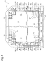
- a solid-state imaging device 1 is used for a so-called passive CMOS image sensor, and is a semiconductor element for which a plurality of pixels are two-dimensionally arranged.
- the solid-state imaging device 1 includes a light receiving section 10, a signal output section 20 including a plurality of output parts 20a, and a vertical shift register 30 including a plurality of shift register parts 30a.
- the light receiving section 10, the signal output section 20, and the vertical shift register 30 are built in the main surface of a semiconductor substrate 14 such as, for example, a silicon substrate.
- this semiconductor substrate 14 may be bonded to a base member having a flat-plate shape to maintain mechanical strength.
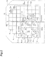
- the light receiving section 10 is configured by two-dimensionally arranging the plurality of pixels 11 in M rows and N columns (M and N are each an integer not less than 2). That is, the light receiving section 10 has a plurality of pixels 11 two-dimensionally arrayed so that the light receiving section 10 has M rows and N columns.
- the light receiving section 10 of the present embodiment is configured such that L (L ⁇ 2) row groups A 1 to A L each having a plurality of rows that have the same number or quantity of columns are arranged in the column direction. That is, the light receiving section 10 includes L row groups A 1 to A L which are arrayed in the column direction and each of which has a plurality of pixel rows.
- each of the row groups A 1 to A L a plurality of rows contained in that row group have the same number or quantity of pixels as each other.
- Each of the row groups A 1 to A L is configured with a plurality of pixel groups 10a arranged in the row direction, as the range of a row group A L-1 is shown by an alternate long and short dashed line in Fig. 2 , for example.
- Each of the pixel groups 10a is configured with a plurality of pixels 11 two-dimensionally arrayed in Ma rows and Na columns (25 ⁇ Ma ⁇ M, 2 ⁇ Na ⁇ N).
- the pixel group 10a is a unit of exposure when producing the light receiving unit 10 by a photolithography technique.
- the number of pixel groups 10a contained in the row group A L located at one end in the column direction out of the L row groups A 1 to A L is provided as n.
- the number of pixel groups 10a contained in the row group A L-2 is (n+4)
- the number of pixel groups 10a contained in the respective row groups A L-2 to A 1 from the row group A L-2 to the row group A 1 of the other end is constant, and the numbers or quantities of columns N L-2 to N 1 of the pixels 11 contained in these row groups A L-2 to A 1 are all equal, (n+4) ⁇ Na.
- the respective quantities of columns N L-2 to N L of the three consecutive row groups A L-2 to A L including the row group A L located at one end in the column direction are increased in order from the side of the row group A L , and satisfy a relationship of N L ⁇ N L-1 ⁇ N L-2 .
- the contour of the light receiving section 10 defined by the row groups A L-2 to A L that is, the contour between the side 10b and the sides 10c and 10d of the light receiving section 10, has a stepped shape.
- the pixels 11 of the light receiving section 10 are of the PPS type, and have a common configuration. That is, each of the pixels 11 includes a photodiode PD and a readout switch SWa.
- the anode terminal of the photodiode PD is grounded, and the cathode terminal of the photodiode PD is connected to a readout line 12 via the readout switch SWa.
- the photodiode PD generates charge of an amount according to an incident light intensity, and accumulates the generated charge in a junction capacitance section.
- the readout switch SWa is supplied with a row selection control signal via a row selection line 13.
- the row selection control signal is a signal that instructs an opening and closing operation of the readout switches SWa of the pixels 11 included in the respective rows of the light receiving section 10.
- the readout switch SWa opens, and a charge generated in the photodiode PD is not output to the readout line 12 but is accumulated in the junction capacitance section.
- the readout switch SWa closes, and the charge generated in the photodiode PD and accumulated in the junction capacitance section until then is output to the readout line 12 through the readout switch SWa.
- the vertical shift registers 30 are disposed at both ends of the light receiving section 10 in the row direction.
- the vertical shift register 30 is provided for controlling charge outputs from the pixels 11 shown in Fig. 2 for each of the rows, and supplies row selection control signals to the respective pixels 11 via the row selection lines 13.
- the vertical shift register 30 is configured with a plurality of shift register parts 30a provided in association with the L row groups A 1 to A L described above.
- L shift register parts 30a are arranged at one end side of the row groups A 1 to A L in the row direction, and other L shift register parts 30a are disposed at the other end side.
- Each of the respective shift register parts 30a is arranged along the end column of the corresponding row group, and connected to Ma row selection lines 13 of that row group.
- the signal output section 20 is arranged adjacent to one side (specifically, one side defined by the row group A 1 ) of the light receiving section 10 extending along the row direction.
- the signal output section 20 is connected with readout lines 12 disposed in association with the respective columns of the light receiving section 10, and outputs voltage values (analog or digital values) according to the amounts of charge input through the readout lines 12.
- the signal output section 20 is configured with a plurality of output parts 20a provided in association with a plurality of pixel groups 10a that form the row group A 1 described above.
- the respective output parts 20a are connected to Na readout lines 12 of corresponding pixel groups 10a, respectively.
- the solid-state imaging device 1 of the present embodiment further includes a plurality of terminal electrodes 40.
- the terminal electrodes 40 are arranged in an edge portion of the semiconductor substrate 14 along the signal output section 20, for example. Some of the terminal electrodes 40 are connected to the signal output section 20, and are input with a reset signal to reset an integration circuit included in the signal output section 20, a hold signal to control signal input to a holding circuit included in the signal output section 20, a horizontal start signal to start operation of a horizontal shift register included in the signal output section 20, a horizontal clock signal that defines a clock of the horizontal shift register, and a supply voltage to drive the signal output section 20 from outside of the solid-state imaging device 1, and output a voltage signal output from the signal output section 20 to the outside of the solid-state imaging device 1.
- terminal electrodes 40 are connected to the respective shift register parts 30a of the vertical shift register 30 via a trunk line 50. These terminal electrodes 40 are input with a gate signal, a vertical start signal, a vertical clock signal, and a supply voltage to drive the respective shift register parts 30a, respectively, to be used in the vertical shift register 30, for example.
- the trunk line 50 is a line group including a plurality of lines provided extending along the column direction of the light receiving section 10 in order to supply signals and electrical power to the respective shift register parts 30a corresponding to the respective row groups A 1 to A L , of the light receiving section 10.
- the trunk line 50 in the present embodiment refers to, out of the lines to supply signals and electrical power to the vertical shift register 30, a line (or line group) common to a plurality of parts included in the vertical shift register 30, and lines extending to the respective shift register parts 30a of the vertical shift register 30 having branched off from the common line are not included therein.
- the solid-state imaging device 1 includes a plurality of buffer amplifiers 61 provided corresponding to the respective row groups A 1 to A L , and the trunk line 50 and the respective shift register parts 30a may be connected to each other via corresponding buffer amplifiers 61, respectively.
- a buffer amplifier 62 may be connected between the terminal electrode 40 and the trunk line 50.
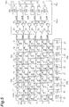
- Fig. 3 is a plan view showing a peripheral configuration of that part
- Fig. 4 is a side sectional view showing the main part of a section along a line IV-IV of Fig. 3 .
- the solid-state imaging device 1 further includes a dummy photodiode region 70 in addition to the above-described configuration.
- the dummy photodiode region 70 is a region to absorb light incident outside of the light receiving section 10 and eliminate generated carriers, and is formed mainly along the stepped contour of the light receiving section 10.
- the dummy photodiode region 70 has the same semiconductor layer structure as that of the photodiodes PD of the respective pixels 11. Specifically, as shown in Fig. 4 , the photodiodes PD of the respective pixels 11 have a second conductivity-type (for example, n-type) semiconductor layer 16 being an ion injection layer, formed on the surface side of a first conductivity-type semiconductor region 15 having a first conductivity type (for example, p-type) and to serve as a base of the semiconductor substrate 14.
- a second conductivity-type (for example, n-type) semiconductor layer 16 being an ion injection layer
- the second conductivity-type semiconductor layer 16 and the first conductivity-type semiconductor region 15 form a p-n junction with each other, and the second conductivity-type semiconductor layer 16 serves as a light detecting region on which an image of light is made incident to generate charge (carriers).
- the second conductivity-type semiconductor layers 16 of the respective pixels 11 are isolated from each other by an oxide film (LOCOS; Local Oxidation of Silicon) 17.
- LOCS Local Oxidation of Silicon
- the dummy photodiode region 70 is also the same in configuration as the photodiode PD, and has a second conductivity-type semiconductor layer 71 being an ion injection layer formed on the surface side of the first conductivity-type semiconductor region 15.
- the second conductivity-type semiconductor layer 71 and the first conductivity-type semiconductor region 15 form a p-n junction with each other, and when light and radiation made incident on the surroundings of the light receiving section 10 are made incident onto the second conductivity-type semiconductor layer 71, a charge is generated.
- the second conductivity-type semiconductor layer 71 is connected to a reference potential (ground potential) via an electrode included in a plurality of terminal electrodes 40, for example, and a generated charge is discharged to the outside as unnecessary carriers via that electrode.
- the respective pixels 11 of the light receiving section 10 and the dummy photodiode region 70, and further the respective components on the semiconductor substrate 14 excluding the terminal electrodes 40, such as the signal output section 20, the vertical shift register 30, and the trunk line 50 are covered with a passivation film 80 shown in Fig. 4 , and protected.
- the dummy photodiode region 70 having such a configuration includes, as shown in Fig. 3 , partial regions 70a, partial regions 70b, partial regions 70c, and partial regions 70d.
- a plurality of partial regions 70a are formed between the respective shift register parts 30a corresponding to the respective row groups A 1 to A L of the light receiving section 10 and the row groups A 1 to A L , respectively, and the respective partial regions 70a extend along the end columns of the respective row groups A 1 to A L .
- the photodiodes PD in the end columns of the respective row groups A 1 to A L and the partial regions 70a, and the respective shift register parts 30a and the partial regions 70a are separated from each other by the oxide films 17 provided therebetween, respectively.
- a plurality of partial regions 70b are formed mainly between the respective shift register parts 30a and the trunk line 50, respectively, and the respective partial regions 70b are provided extending along an inner edge of the trunk line 50 when viewed from the direction vertical to a substrate plane of the semiconductor substrate 14.
- a part of the trunk line 50 extending along one-side ends of the row groups A 1 to A L-2 that is, a linear contour of the light receiving section 10 extends straight along the column direction.
- a part extending in the row direction and a part extending in the column direction are alternately linked, so that the trunk line 50 also shows a stepped shape.
- the partial region 70b is formed not only in a region along apart extending in the column direction of the trunk line 50, but also in a region along a part extending in the row direction.
- Each of the plurality of partial regions 70c is formed along an edge at the outside (that is, the side opposite to where the partial regions 70b are formed) of the trunk line 50.
- the partial regions 70c have their shapes and areas greatly different from each other, depending on the corresponding row groups. That is, the partial regions 70c corresponding to the row groups A 1 to A L-2 that form a linear contour of the light receiving section 10 extend along the trunk line 50 extending in the column direction, and have an elongated shape having its longitudinal direction in the column direction in a relatively narrow region between an edge of the semiconductor substrate 14 and the trunk line 50.
- the partial regions 70c corresponding to the row groups A L-1 to A L that form a stepped contour of the light receiving section 10 extend along both of the part extending in the row direction of the trunk line 50 and the part extending in the row direction, and has a wide shape having its longitudinal direction in the row direction in a relatively wide region between the edge of the semiconductor substrate 14 and the trunk line 50.
- the partial regions 70b and 70c described above are formed along both sides of the trunk line 50, and not formed directly under the trunk line 50.
- an oxide film 17 as shown in Fig. 4 , and the trunk line 50 and the first conductivity-type semiconductor region 15 are insulated from each other by this oxide film 17.
- the oxide film 17 is formed thicker than the second conductivity-type semiconductor layer 71 of the dummy photodiode region 70, and parasitic capacitance of the trunk line 50 is reduced by sufficiently securing the distance between the trunk line 50 and the first conductivity-type semiconductor region 15.
- the branch lines extending from the trunk line 50 via the buffer amplifiers 61 to the shift register parts 30a are partially formed on the second conductivity-type semiconductor layer 71 that forms the partial region 70b since the effect of parasitic capacitance is negligible.
- a plurality of partial regions 70d are arranged along one side, of a pair of sides of the light receiving section 10 extending along the row direction, opposite to the side along which the signal output section 20 is provided, and are respectively provided adjacent to a plurality of pixel groups 10a that form the row group A L .
- the arrangement of the partial regions 70a to 70d described above is simply realized, when forming the shift register parts 30a etc., at both ends of the respective row groups A 1 to A L by a photolithography technique, by simultaneously forming the partial regions 70a to 70d one each for each of the unit regions of exposure.
- Fig. 5 is a circuit diagram showing in greater detail a configuration of two pixel groups 10a included in a certain row group of the light receiving section 10 and a configuration of a shift register part 30a corresponding to that row group.
- the shift register part 30a includes a plurality of shift registers 31 mutually connected in series, and NOR circuits (NOR gates) 32 and buffers 33 provided corresponding to the respective rows contained in the row group of the light receiving section 10.
- NOR circuits NOR gates
- buffers 33 provided corresponding to the respective rows contained in the row group of the light receiving section 10.
- a vertical clock signal Ckv that defines operation clocks of the respective shift registers 31 is supplied via the trunk line 50 (refer to Fig. 1 ).
- a vertical start signal Spv to start operation of the vertical shift register 30 is supplied via the trunk line 50.
- output terminals of the respective Ma pixels 11 that configures each row of the pixel group 10a are connected, via the readout line 12, to the output part 20a corresponding to the pixel group 10a (concretely, integration circuits 21 provided for each of the columns in the output parts 20a).
- Fig. 6 is a circuit diagram showing a concrete configuration of circuits connected to each readout line 12 in an output part 20a of the signal output section 20.
- a circuit configuration of the output part 20a corresponding to a single readout line 12 is shown.
- the output part 20a has an integration circuit 21 and a holding circuit 22 provided for each of the readout lines 12.
- the integration circuit 21 includes an amplifier AM, an integrating capacitive element C 1 , and a discharge switch SW 1 .
- the integrating capacitive element C 1 and the discharge switch SW 1 are connected in parallel to each other, and provided between an input terminal and an output terminal of the amplifier AM.
- the input terminal of the amplifier AM is connected with the corresponding readout line 12.
- the discharge switch SW 1 is supplied with a discharge control signal Reset from a control circuit (not shown).
- the discharge control signal Reset is a signal that controls collectively an opening and closing operation of the discharge switch SW 1 of each of the integration circuits 21 included in the output part 20a.
- the discharge switch SW 1 closes, the integrating capacitive element C 1 is discharged, and a voltage value to be output from the integration circuit 21 is initialized.
- the discharge switch SW 1 opens, a charge input to the input terminal is accumulated in the integrating capacitive element C 1 , and a voltage value according to the accumulated charge amount is output from the integration circuit 21.
- the holding circuit 22 includes an input switch SW 21 , an output switch SW 22 , and a holding capacitive element C 2 .
- One end of the holding capacitive element C 2 is grounded.
- the other end of the holding capacitive element C 2 is connected with the output terminal of the integration circuit 21 via the input switch SW 21 , and connected with a voltage output line 18 via the output switch SW 22 .
- the input switch SW 21 is supplied with a hold control signal Hold from the control circuit (not shown).
- the hold control signal Hold is a signal that controls collectively an opening and closing operation of the input switch SW 21 of each of the holding circuits 22 included in the output part 20a.
- the output switch SW 22 is supplied with an n-th column selection control signal Hsel(n) from the control circuit (not shown).
- the n-th column selection control signal Hsel(n) is a signal that controls for each of the columns an opening and closing operation of the output switch SW 22 included in the holding circuit 22.
- the input switch SW 21 switches from a closed state to an open state, and a voltage value being input to the input terminal at this time is held in the holding capacitive element C 2 .
- the output switch SW 22 closes, and the voltage value held in the holding capacitive element C 2 is output to the voltage output line 18.
- the arrangement of the pixel groups 10a contained in the light receiving section 10 are devised, so that the contour between one side 10b along the row direction of the light receiving section 10 and a pair of sides 10c and 10d along the column direction (that is, the contour of a part equivalent to two corners of the rectangular light receiving section 10) has a stepped shape.
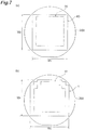
- Figs. 7 are views showing states where a solid-state imaging device is arranged on a substantially circular semiconductor wafer 200, in which a state where a conventional solid-state imaging device 80 with a rectangular light receiving section 90 is arranged is shown in the area (a) of Fig. 7 , and a state where the solid-state imaging device 1 of the present embodiment is arranged is shown in area (b) of Fig. 7 .
- a solid-state imaging device is generally cut out by dicing of the substantially circular semiconductor wafer 200 as shown in Figs. 7 , but as shown in the area (a) of Fig.
- the outline of the solid-state imaging device 80 results in a rectangular shape (a width W 1 in the row direction, a width W 2 in the column direction) that inscribes an outer edge of the substantially circular semiconductor wafer 200.
- a width W 1 in the row direction a width W 2 in the column direction
- the solid-state imaging device 1 of the present embodiment as a result of providing the contour of two corners of the light receiving section 10 in a stepped shape, the contour of a corresponding part of the solid-state imaging device 1 also results in a stepped shape, the solid-state imaging device 1 can be provided with a width W 3 in the row direction and a width W 4 in the column direction that are longer than the widths W 1 and W 2 , respectively, and even in consideration of the area of the part cut away in a stepped shape, the light receiving section 10 can be provided with a larger area.
- the light receiving section 10 of a larger area can be obtained under limitations due to the size of the semiconductor wafer 20 to serve as material.
- the dummy photodiode region 70 is formed along the stepped contour of the light receiving section 10. Therefore, unnecessary carriers generated in the periphery of the stepped light receiving section 10 can be eliminated in this dummy photodiode region 70. Therefore, by the solid-state imaging device 1 of the present embodiment, flowing of unnecessary carriers into the light receiving section 10 can be prevented, noise can be reduced, and degradation in uniformity of the light receiving section 10 can be suppressed.
- the light receiving section 10 is configured such that L (L ⁇ 2) row groups A 1 to A L each having a plurality of pixel rows are arranged in the column direction, and the stepped contour of the light receiving section 10 may be realized by the quantities of columns N L-LA+1 to N L of the consecutive LA (2 ⁇ LA ⁇ L) row groups A L-LA+1 to A L including the row group A L (number or quantity of columns of N L ) located at one end in the column direction out of the L row groups A 1 to A L satisfying N L ⁇ N L-1 ⁇ ... ⁇ N L-LA+1 .
- the stepped contour of the light receiving section 10 can be suitably formed.
- the partial regions 70a of the dummy photodiode region 70 are formed between the respective shift register parts 30a of the vertical shift register 30 and the corresponding respective row groups A 1 to A L . Since the unnecessary carriers described above can be generated also in the vertical shift register 30, by thus arranging the partial regions 70a of the dummy photodiode region 70, unnecessary carriers to flow into the light receiving section 10 can be more reliably eliminated.
- the partial regions 70b and 70c of the dummy photodiode region 70 may be formed along both sides of the trunk line 50, that is, formed in a region except directly under the trunk line 50.
- the interval between the trunk line 50 and the semiconductor substrate 14 can be sufficiently secured to suppress an increase in parasitic capacitance of the trunk line 50 and a signal delay involved.
- a large-area solid-state imaging device 1 since the length of the trunk line 50 is elongated because of the large area, and a signal delay is likely to occur, such a device can be applied.
- the trunk line 50 and the respective shift register parts 30a are connected via the buffer amplifiers 61 corresponding to the respective row groups A 1 to A L of the light receiving section 10.
- the trunk line 50 is elongated.
- the elongated trunk line 50 serves as a capacitance load, which easily causes a signal delay.
- wiring is carried out for a very large number of gate switches from the single trunk line 50, and this leads to an increase in capacitance load, and a signal delay more easily occurs.
- the dummy photodiode region 70 may have the same semiconductor layer structure as that of the photodiodes PD of the respective pixels 11. Thereby, the dummy photodiode region 70 may be easily formed without adding a special process when producing the solid-state imaging device 1.
- the solid-state imaging device 1 according to the present embodiment as a result of a scintillator being provided at the front of the light receiving section 10, can be suitably used in an X-ray CT apparatus, for example. Therefore, an example of an X-ray CT apparatus being useful to understand the present invention and including the solid-state imaging device 1 according to the present embodiment will be described in the following.
- Fig. 8 is a configuration diagram of an X-ray CT apparatus 100 according to an example being useful to understand the present invention.
- an X-ray source 106 generates X-rays toward a subject.
- the radiation field of X-rays generated from the X-ray source 106 is controlled by a primary slit plate 106b.
- the X-ray source 106 has a built-in X-ray tube, and by adjusting conditions of the X-ray tube, such as a tube voltage, a tube current, and energization time, the X-ray dose to the subject is controlled.
- An X-ray image sensor 107 is equivalent to the solid-state imaging device 1 according to the present embodiment, is provided with a scintillator panel at the front of its light receiving section 10, and images an X-ray image transmitted through the subject.
- a secondary slit plate 107a that limits an X-ray incident region is provided.
- a swing arm 104 holds the X-ray source 106 and the X-ray image sensor 107 so as to be opposed, and swings these around the subject in panoramic tomography. Moreover, in the case of linear tomography, a sliding mechanism 113 for linearly displacing the X-ray image sensor 107 with respect to the subject is provided.
- the swing arm 104 is driven by an arm motor 110 that forms a rotary table, and a rotation angle thereof is detected by an angle sensor 112.
- the arm motor 110 is mounted on a movable portion of an XY table 114, and the center of rotation is arbitrarily adjusted in a horizontal plane.
- a CRT cathode ray tube
- the CPU 121 is connected with a work memory 123 required for signal processing, and further connected with an operation panel 119 having a panel switch, an X-ray irradiation switch, etc. Moreover, the CPU 121 is connected to a motor drive circuit 111 that drives the arm motor 110, slit control circuits 115, 116 that control the opening range of the primary slit plate 106b and the secondary slit plate 107a, an X-ray control circuit 118 that controls the X-ray source 106, respectively, and further outputs a clock signal to drive the X-ray image sensor 107.
- the X-ray control circuit 118 is capable of feedback-controlling the X-ray dose to the subject based on signals imaged by the X-ray image sensor 107.
- the X-ray CT apparatus 100 as a result of including the solid-state imaging device 1 according to the present embodiment, can have a light receiving section of a larger area. Moreover, flowing of unnecessary carriers into the light receiving section can be prevented, noise can be reduced, and degradation in uniformity of the light receiving section can be suppressed.
- 1 ... solid-state imaging device 10 ... light receiving section, 10a ... pixel group, 11 ... pixel, 12 ... readout line, 13 ... row selection line, 14 ... semiconductor substrate, 15 ... first conductivity-type semiconductor region, 16 ... second conductivity-type semiconductor layer, 17 ... oxide film, 18 ... voltage output line, 20 ... signal output section, 20a ... output part, 21 ... integration circuit, 22 ... holding circuit, 30 ... horizontal shift register, 30a ... shift register part, 31 ... shift register, 32 ... gate, 33 ... buffer, 40 ... terminal electrode, 50 ... trunk line, 61, 62 ... buffer amplifier, 70 ... dummy photodiode region, 70a to 70d ... partial region, 71 ... second conductivity-type semiconductor layer, 80 ... passivation film, 200 ... semiconductor wafer, A 1 to A L ... row group.
Landscapes
- Engineering & Computer Science (AREA)
- Health & Medical Sciences (AREA)
- Life Sciences & Earth Sciences (AREA)
- Medical Informatics (AREA)
- Signal Processing (AREA)
- Multimedia (AREA)
- Physics & Mathematics (AREA)
- Biomedical Technology (AREA)
- Animal Behavior & Ethology (AREA)
- Optics & Photonics (AREA)
- Pathology (AREA)
- Radiology & Medical Imaging (AREA)
- High Energy & Nuclear Physics (AREA)
- Heart & Thoracic Surgery (AREA)
- Molecular Biology (AREA)
- Surgery (AREA)
- Nuclear Medicine, Radiotherapy & Molecular Imaging (AREA)
- General Health & Medical Sciences (AREA)
- Public Health (AREA)
- Veterinary Medicine (AREA)
- Biophysics (AREA)
- Mathematical Physics (AREA)
- Dentistry (AREA)
- Oral & Maxillofacial Surgery (AREA)
- Solid State Image Pick-Up Elements (AREA)
- Transforming Light Signals Into Electric Signals (AREA)
- Apparatus For Radiation Diagnosis (AREA)
Claims (5)
- Festkörper-Bildgebungsvorrichtung (1), umfassend:einen Lichtempfangsabschnitt (10) mit einer Vielzahl von Pixeln (11), aufweisend Fotodioden (PD), wobei die Pixel (11) jeweils zweidimensional in M-Zeilen und N-Spalten angeordnet sind,wobeieine Kontur zwischen einer Seite des Lichtempfangsabschnitts (10), die sich entlang einer Zeilenrichtung erstreckt, und einem Paar von Seiten des Lichtempfangsabschnitts (10), die sich entlang einer Spaltenrichtung erstrecken, eine Stufenform hat; undein Attrappen-Fotodiodenbereich (70), gebildet entlang der Stufenkontur des Lichtempfangsabschnitts (10), wobei der Attrappen-Fotodiodenbereich (70) ein Bereich ist, der konfiguriert ist, Träger zu eliminieren, die in der Peripherie des gestuften Lichtempfangsabschnitts (10) erzeugt wurden,dadurch gekennzeichnet, dassdie Festkörper-Bildgebungsvorrichtung weiter umfasstN-Ausleseleitungen (12), angeordnet für die jeweiligen Spalten und verbunden mit den Fotodioden (PD) aufgewiesen in den Pixeln (11) der jeweiligen Spalten mittels Ausleseschaltern (SWa); undeinen Signalausgabeabschnitt (20) zum Ausgeben eines Spannungswertes gemäß einer Ladungseingangsmenge durch jede der Ausleseleitungen (12); undein vertikales Schieberegister (30) zur Steuerung einer Öffnungs- und Schließoperation des Ausleseschalters (SWa) für jede der Zeilen; undwobeider Lichtempfangsabschnitt (10) so konfiguriert ist, dass L-Zeilengruppen (A1-AL),von denen jede eine Vielzahl von Zeilen aufweist, die dieselbe Anzahl von Spalten hat und in der Spaltenrichtung angeordnet ist, wobei L≥2,Anzahlen von Spalten NL-LA+1 bis NL von aufeinanderfolgenden LA-Zeilengruppen,aufweisend eine Zeilengruppe, die eine Anzahl von Spalten NL hat und sich an einem Ende in der Spaltenrichtung befindet, außerhalb der L-Zeilengruppen NL<NL-1<...<NL-LA+1 erfüllt, die Kontur des Lichtempfangsabschnitts (10) mit der Stufenform bilden, wobei 2≤LA<L,das vertikale Schieberegister (30) aus einer Vielzahl von Schieberegisterteilen (30a) gebildet ist, wobei jedes der jeweiligen Schieberegisterteile entlang einer Endspalte der entsprechenden Zeilengruppe angeordnet ist und jede der L-Zeilengruppen mit einem jeweiligen Schieberegisterteil (30a) verbunden ist, angeordnet entlang der entsprechenden Endspalte dieser Zeilengruppe,undmindestens ein Teil (70a) des Attrappen-Fotodiodenbereichs (70) zwischen den jeweiligen Schieberegisterteilen (30a) des vertikalen Schieberegisters (30) gebildet ist, entsprechend den jeweiligen Zeilengruppen des Lichtempfangsabschnitts (10) und den Zeilengruppen.
- Festkörper-Bildgebungsvorrichtung nach Anspruch 1, weiter umfassend eine Hauptleitung (50), die sich entlang der Spaltenrichtung des Lichtempfangsabschnitts (10) erstreckend angeordnet ist, um den jeweiligen Teilen des vertikalen Schieberegisters (30), entsprechend jeweiligen Zeilengruppen des Lichtempfangsabschnitts (10), Signale und elektrische Energie bereitzustellen, wobei
die Hauptleitung (50), unter Leitungen, um dem vertikalen Schieberegister (30) Signale und elektrische Energie bereitzustellen, eine Leitung oder eine Leitungsgruppe ist, gemeinsam mit einer Vielzahl von Teilen aufgewiesen im vertikalen Schieberegister (30), und
mindestens ein Teil des Attrappen-Fotodiodenbereichs (70) entlang beiden Seiten der Hauptleitung (50) gebildet ist. - Festkörper-Bildgebungsvorrichtung nach Anspruch 1, weiter umfassend eine Hauptleitung (50), die sich entlang der Spaltenrichtung des Lichtempfangsabschnitts (10) erstreckend vorgesehen ist, um den jeweiligen Teilen des vertikalen Schieberegisters (30), entsprechend den jeweiligen Zeilengruppen des Lichtempfangsabschnitts, Signale und elektrische Energie bereitzustellen, wobei
die Hauptleitung (50), unter Leitungen, um dem vertikalen Schieberegister (30) Signale und elektrische Energie bereitzustellen, eine Leitung oder eine Leitungsgruppe ist, gemeinsam mit einer Vielzahl von Teilen aufgewiesen im vertikalen Schieberegister (30), und der Attrappen-Fotodiodenbereich (70) in einem Bereich gebildet ist, ausgenommen direkt unter der Hauptleitung (50). - Festkörper-Bildgebungsvorrichtung nach Anspruch 2, weiter umfassend eine Vielzahl von Pufferverstärkern (61, 62), entsprechend den jeweiligen Zeilengruppen des Lichtempfangsabschnitts (10), wobei
die Hauptleitung (50) und die Teile des vertikalen Schieberegisters (30) jeweils über die Pufferverstärker (61, 62) verbunden sind. - Festkörper-Bildgebungsvorrichtung nach Anspruch 1, wobei der Attrappen-Fotodiodenbereich (70) dieselbe Halbleiterschichtstruktur hat wie die Fotodiode.
Applications Claiming Priority (2)
| Application Number | Priority Date | Filing Date | Title |
|---|---|---|---|
| JP2009089247A JP5281943B2 (ja) | 2009-04-01 | 2009-04-01 | 固体撮像装置 |
| PCT/JP2010/055418 WO2010113810A1 (ja) | 2009-04-01 | 2010-03-26 | 固体撮像装置 |
Publications (3)
| Publication Number | Publication Date |
|---|---|
| EP2416360A1 EP2416360A1 (de) | 2012-02-08 |
| EP2416360A4 EP2416360A4 (de) | 2013-09-25 |
| EP2416360B1 true EP2416360B1 (de) | 2017-10-11 |
Family
ID=42828101
Family Applications (1)
| Application Number | Title | Priority Date | Filing Date |
|---|---|---|---|
| EP10758582.0A Active EP2416360B1 (de) | 2009-04-01 | 2010-03-26 | Festkörperbildaufnahmevorrichtung |
Country Status (6)
| Country | Link |
|---|---|
| US (2) | US8420995B2 (de) |
| EP (1) | EP2416360B1 (de) |
| JP (1) | JP5281943B2 (de) |
| KR (1) | KR101732196B1 (de) |
| CN (1) | CN102356464B (de) |
| WO (1) | WO2010113810A1 (de) |
Families Citing this family (6)
| Publication number | Priority date | Publication date | Assignee | Title |
|---|---|---|---|---|
| DE102011083689B4 (de) * | 2011-09-29 | 2013-08-08 | Siemens Aktiengesellschaft | Röntgendetektor |
| JP5389970B2 (ja) | 2012-03-26 | 2014-01-15 | シャープ株式会社 | 撮像モジュール、および撮像モジュールの製造方法 |
| JP5886793B2 (ja) * | 2013-06-11 | 2016-03-16 | 浜松ホトニクス株式会社 | 固体撮像装置 |
| JP6285995B2 (ja) * | 2016-08-10 | 2018-02-28 | 浜松ホトニクス株式会社 | 固体撮像装置、放射線撮像システム及び固体撮像装置の制御方法 |
| EP3327612A1 (de) * | 2016-11-24 | 2018-05-30 | Nxp B.V. | Fingerabdruckerfassungssystem und -verfahren |
| US12543390B2 (en) * | 2021-03-11 | 2026-02-03 | National University Corporation Shizuoka University | Radiation imaging device with signal connection wiring between reading chips |
Family Cites Families (18)
| Publication number | Priority date | Publication date | Assignee | Title |
|---|---|---|---|---|
| JP3003944B2 (ja) * | 1990-10-04 | 2000-01-31 | オリンパス光学工業株式会社 | 固体撮像素子 |
| SE503350C2 (sv) * | 1994-09-08 | 1996-05-28 | Regam Medical Systems Ab | Förfarande för utsträckande av den fysiska längden för en rektangulär röntgenstrålningsdetektor |
| JP3424360B2 (ja) * | 1994-12-08 | 2003-07-07 | 株式会社日立製作所 | 固体撮像装置 |
| JP4178608B2 (ja) * | 1998-04-16 | 2008-11-12 | 株式会社ニコン | 固体撮像装置 |
| JP3507800B2 (ja) | 2001-02-02 | 2004-03-15 | 有限会社リニアセル・デザイン | アナログ−デジタル変換器及びこれを用いたイメージセンサ |
| ATE300832T1 (de) * | 2001-05-05 | 2005-08-15 | Manfred Dr Pfeiffer | Gerät zur bilderfassung im oralbereich, insbesondere zur zahnmedizinischen diagnose |
| FR2857160B1 (fr) | 2003-07-01 | 2005-09-23 | Atmel Grenoble Sa | Capteur d'image ergonomique |
| US7460165B2 (en) | 2004-01-09 | 2008-12-02 | Aptina Imaging Corporation | Photo-array layout for monitoring image statistics |
| JP4724760B2 (ja) | 2005-04-11 | 2011-07-13 | 株式会社モリタ製作所 | X線撮影装置 |
| JP2006314774A (ja) | 2005-04-11 | 2006-11-24 | Morita Mfg Co Ltd | スカウトビュー機能を備えたx線撮影装置 |
| WO2006109808A1 (ja) * | 2005-04-11 | 2006-10-19 | J. Morita Manufacturing Corporation | スカウトビュー機能を備えたx線撮影装置 |
| JPWO2006112320A1 (ja) * | 2005-04-15 | 2008-12-11 | 株式会社日立メディコ | X線平面検出器及びx線画像診断装置 |
| JP2006344644A (ja) * | 2005-06-07 | 2006-12-21 | Matsushita Electric Ind Co Ltd | 固体撮像装置およびカメラならびに固体撮像装置の製造方法 |
| FR2888044B1 (fr) * | 2005-07-01 | 2007-08-31 | Atmel Grenoble Soc Par Actions | Capteur d'image a coins coupes |
| JP4669768B2 (ja) | 2005-09-30 | 2011-04-13 | 富士フイルム株式会社 | 解像度可変型x線撮像装置及びx線ct装置 |
| JP4503573B2 (ja) | 2005-10-26 | 2010-07-14 | 株式会社モリタ製作所 | スカウトビュー機能を備えた医療用x線撮影装置 |
| US8237808B2 (en) * | 2007-01-17 | 2012-08-07 | Sony Corporation | Solid state imaging device and imaging apparatus adjusting the spatial positions of pixels after addition by controlling the ratio of weight values during addition |
| JP4963074B2 (ja) * | 2007-03-19 | 2012-06-27 | 国立大学法人 奈良先端科学技術大学院大学 | 計測デバイス |
-
2009
- 2009-04-01 JP JP2009089247A patent/JP5281943B2/ja active Active
-
2010
- 2010-03-26 KR KR1020117013259A patent/KR101732196B1/ko active Active
- 2010-03-26 WO PCT/JP2010/055418 patent/WO2010113810A1/ja not_active Ceased
- 2010-03-26 CN CN201080012808.1A patent/CN102356464B/zh active Active
- 2010-03-26 EP EP10758582.0A patent/EP2416360B1/de active Active
- 2010-03-26 US US13/202,995 patent/US8420995B2/en active Active
-
2013
- 2013-03-13 US US13/799,349 patent/US8704146B2/en active Active
Non-Patent Citations (1)
| Title |
|---|
| None * |
Also Published As
| Publication number | Publication date |
|---|---|
| CN102356464B (zh) | 2014-03-19 |
| US8704146B2 (en) | 2014-04-22 |
| JP2010245110A (ja) | 2010-10-28 |
| US8420995B2 (en) | 2013-04-16 |
| US20130193313A1 (en) | 2013-08-01 |
| EP2416360A4 (de) | 2013-09-25 |
| JP5281943B2 (ja) | 2013-09-04 |
| WO2010113810A1 (ja) | 2010-10-07 |
| KR101732196B1 (ko) | 2017-05-02 |
| KR20110134873A (ko) | 2011-12-15 |
| CN102356464A (zh) | 2012-02-15 |
| US20110303823A1 (en) | 2011-12-15 |
| EP2416360A1 (de) | 2012-02-08 |
Similar Documents
| Publication | Publication Date | Title |
|---|---|---|
| US7514690B2 (en) | Radiation image pickup apparatus and its control method | |
| TWI442906B (zh) | Solid state camera device | |
| US8675813B2 (en) | Solid-state imager and X-ray CT apparatus including same | |
| US8704146B2 (en) | Solid-state imaging device | |
| US8953745B2 (en) | Solid-state image pickup apparatus and X-ray inspection system | |
| JP5714982B2 (ja) | 固体撮像素子の制御方法 | |
| TWI610572B (zh) | 固體攝像裝置 | |
| US20140361180A1 (en) | Radiation image-pickup device and radiation image-pickup display system | |
| US8477907B2 (en) | Solid-state image pickup apparatus and X-ray inspection system | |
| WO2009096313A1 (ja) | 固体撮像装置及びそれを含むx線ct装置 | |
| JP5444444B2 (ja) | 固体撮像装置 | |
| WO2012098801A1 (ja) | 固体撮像装置 | |
| US10212368B2 (en) | Solid-state imaging device | |
| JP2015136159A (ja) | 固体撮像素子の制御方法 | |
| JP2012182836A (ja) | X線検査システム |
Legal Events
| Date | Code | Title | Description |
|---|---|---|---|
| PUAI | Public reference made under article 153(3) epc to a published international application that has entered the european phase |
Free format text: ORIGINAL CODE: 0009012 |
|
| 17P | Request for examination filed |
Effective date: 20110713 |
|
| AK | Designated contracting states |
Kind code of ref document: A1 Designated state(s): AT BE BG CH CY CZ DE DK EE ES FI FR GB GR HR HU IE IS IT LI LT LU LV MC MK MT NL NO PL PT RO SE SI SK SM TR |
|
| DAX | Request for extension of the european patent (deleted) | ||
| A4 | Supplementary search report drawn up and despatched |
Effective date: 20130823 |
|
| RIC1 | Information provided on ipc code assigned before grant |
Ipc: H01L 27/148 20060101ALI20130819BHEP Ipc: H01L 27/14 20060101ALI20130819BHEP Ipc: H04N 5/335 20110101ALI20130819BHEP Ipc: H01L 27/146 20060101AFI20130819BHEP Ipc: A61B 6/00 20060101ALI20130819BHEP |
|
| STAA | Information on the status of an ep patent application or granted ep patent |
Free format text: STATUS: EXAMINATION IS IN PROGRESS |
|
| 17Q | First examination report despatched |
Effective date: 20170303 |
|
| GRAP | Despatch of communication of intention to grant a patent |
Free format text: ORIGINAL CODE: EPIDOSNIGR1 |
|
| STAA | Information on the status of an ep patent application or granted ep patent |
Free format text: STATUS: GRANT OF PATENT IS INTENDED |
|
| RIC1 | Information provided on ipc code assigned before grant |
Ipc: A61B 6/14 20060101ALN20170503BHEP Ipc: A61B 6/00 20060101ALI20170503BHEP Ipc: H04N 5/374 20110101ALI20170503BHEP Ipc: H04N 5/335 20110101ALI20170503BHEP Ipc: H01L 27/146 20060101AFI20170503BHEP Ipc: H04N 5/32 20060101ALI20170503BHEP Ipc: H01L 27/148 20060101ALI20170503BHEP |
|
| RIC1 | Information provided on ipc code assigned before grant |
Ipc: H04N 5/32 20060101ALI20170516BHEP Ipc: H01L 27/148 20060101ALI20170516BHEP Ipc: H01L 27/146 20060101AFI20170516BHEP Ipc: H04N 5/374 20110101ALI20170516BHEP Ipc: H04N 5/335 20110101ALI20170516BHEP Ipc: A61B 6/14 20060101ALN20170516BHEP Ipc: A61B 6/00 20060101ALI20170516BHEP |
|
| INTG | Intention to grant announced |
Effective date: 20170531 |
|
| RIN1 | Information on inventor provided before grant (corrected) |
Inventor name: MORI, HARUMICHI Inventor name: FUJITA, KAZUKI Inventor name: KYUSHIMA, RYUJI |
|
| GRAS | Grant fee paid |
Free format text: ORIGINAL CODE: EPIDOSNIGR3 |
|
| GRAA | (expected) grant |
Free format text: ORIGINAL CODE: 0009210 |
|
| STAA | Information on the status of an ep patent application or granted ep patent |
Free format text: STATUS: THE PATENT HAS BEEN GRANTED |
|
| AK | Designated contracting states |
Kind code of ref document: B1 Designated state(s): AT BE BG CH CY CZ DE DK EE ES FI FR GB GR HR HU IE IS IT LI LT LU LV MC MK MT NL NO PL PT RO SE SI SK SM TR |
|
| REG | Reference to a national code |
Ref country code: GB Ref legal event code: FG4D |
|
| REG | Reference to a national code |
Ref country code: CH Ref legal event code: EP |
|
| REG | Reference to a national code |
Ref country code: IE Ref legal event code: FG4D |
|
| REG | Reference to a national code |
Ref country code: AT Ref legal event code: REF Ref document number: 936738 Country of ref document: AT Kind code of ref document: T Effective date: 20171115 |
|
| REG | Reference to a national code |
Ref country code: DE Ref legal event code: R096 Ref document number: 602010045897 Country of ref document: DE |
|
| REG | Reference to a national code |
Ref country code: CH Ref legal event code: NV Representative=s name: SERVOPATENT GMBH, CH |
|
| REG | Reference to a national code |
Ref country code: NL Ref legal event code: MP Effective date: 20171011 |
|
| REG | Reference to a national code |
Ref country code: FR Ref legal event code: PLFP Year of fee payment: 9 |
|
| REG | Reference to a national code |
Ref country code: LT Ref legal event code: MG4D |
|
| REG | Reference to a national code |
Ref country code: AT Ref legal event code: MK05 Ref document number: 936738 Country of ref document: AT Kind code of ref document: T Effective date: 20171011 |
|
| PG25 | Lapsed in a contracting state [announced via postgrant information from national office to epo] |
Ref country code: NL Free format text: LAPSE BECAUSE OF FAILURE TO SUBMIT A TRANSLATION OF THE DESCRIPTION OR TO PAY THE FEE WITHIN THE PRESCRIBED TIME-LIMIT Effective date: 20171011 |
|
| PG25 | Lapsed in a contracting state [announced via postgrant information from national office to epo] |
Ref country code: NO Free format text: LAPSE BECAUSE OF FAILURE TO SUBMIT A TRANSLATION OF THE DESCRIPTION OR TO PAY THE FEE WITHIN THE PRESCRIBED TIME-LIMIT Effective date: 20180111 Ref country code: ES Free format text: LAPSE BECAUSE OF FAILURE TO SUBMIT A TRANSLATION OF THE DESCRIPTION OR TO PAY THE FEE WITHIN THE PRESCRIBED TIME-LIMIT Effective date: 20171011 Ref country code: LT Free format text: LAPSE BECAUSE OF FAILURE TO SUBMIT A TRANSLATION OF THE DESCRIPTION OR TO PAY THE FEE WITHIN THE PRESCRIBED TIME-LIMIT Effective date: 20171011 Ref country code: SE Free format text: LAPSE BECAUSE OF FAILURE TO SUBMIT A TRANSLATION OF THE DESCRIPTION OR TO PAY THE FEE WITHIN THE PRESCRIBED TIME-LIMIT Effective date: 20171011 |
|
| PG25 | Lapsed in a contracting state [announced via postgrant information from national office to epo] |
Ref country code: IS Free format text: LAPSE BECAUSE OF FAILURE TO SUBMIT A TRANSLATION OF THE DESCRIPTION OR TO PAY THE FEE WITHIN THE PRESCRIBED TIME-LIMIT Effective date: 20180211 Ref country code: BG Free format text: LAPSE BECAUSE OF FAILURE TO SUBMIT A TRANSLATION OF THE DESCRIPTION OR TO PAY THE FEE WITHIN THE PRESCRIBED TIME-LIMIT Effective date: 20180111 Ref country code: AT Free format text: LAPSE BECAUSE OF FAILURE TO SUBMIT A TRANSLATION OF THE DESCRIPTION OR TO PAY THE FEE WITHIN THE PRESCRIBED TIME-LIMIT Effective date: 20171011 Ref country code: HR Free format text: LAPSE BECAUSE OF FAILURE TO SUBMIT A TRANSLATION OF THE DESCRIPTION OR TO PAY THE FEE WITHIN THE PRESCRIBED TIME-LIMIT Effective date: 20171011 Ref country code: LV Free format text: LAPSE BECAUSE OF FAILURE TO SUBMIT A TRANSLATION OF THE DESCRIPTION OR TO PAY THE FEE WITHIN THE PRESCRIBED TIME-LIMIT Effective date: 20171011 Ref country code: GR Free format text: LAPSE BECAUSE OF FAILURE TO SUBMIT A TRANSLATION OF THE DESCRIPTION OR TO PAY THE FEE WITHIN THE PRESCRIBED TIME-LIMIT Effective date: 20180112 |
|
| REG | Reference to a national code |
Ref country code: DE Ref legal event code: R097 Ref document number: 602010045897 Country of ref document: DE |
|
| PG25 | Lapsed in a contracting state [announced via postgrant information from national office to epo] |
Ref country code: EE Free format text: LAPSE BECAUSE OF FAILURE TO SUBMIT A TRANSLATION OF THE DESCRIPTION OR TO PAY THE FEE WITHIN THE PRESCRIBED TIME-LIMIT Effective date: 20171011 Ref country code: DK Free format text: LAPSE BECAUSE OF FAILURE TO SUBMIT A TRANSLATION OF THE DESCRIPTION OR TO PAY THE FEE WITHIN THE PRESCRIBED TIME-LIMIT Effective date: 20171011 Ref country code: CZ Free format text: LAPSE BECAUSE OF FAILURE TO SUBMIT A TRANSLATION OF THE DESCRIPTION OR TO PAY THE FEE WITHIN THE PRESCRIBED TIME-LIMIT Effective date: 20171011 Ref country code: SK Free format text: LAPSE BECAUSE OF FAILURE TO SUBMIT A TRANSLATION OF THE DESCRIPTION OR TO PAY THE FEE WITHIN THE PRESCRIBED TIME-LIMIT Effective date: 20171011 |
|
| PLBE | No opposition filed within time limit |
Free format text: ORIGINAL CODE: 0009261 |
|
| STAA | Information on the status of an ep patent application or granted ep patent |
Free format text: STATUS: NO OPPOSITION FILED WITHIN TIME LIMIT |
|
| PG25 | Lapsed in a contracting state [announced via postgrant information from national office to epo] |
Ref country code: PL Free format text: LAPSE BECAUSE OF FAILURE TO SUBMIT A TRANSLATION OF THE DESCRIPTION OR TO PAY THE FEE WITHIN THE PRESCRIBED TIME-LIMIT Effective date: 20171011 Ref country code: SM Free format text: LAPSE BECAUSE OF FAILURE TO SUBMIT A TRANSLATION OF THE DESCRIPTION OR TO PAY THE FEE WITHIN THE PRESCRIBED TIME-LIMIT Effective date: 20171011 Ref country code: RO Free format text: LAPSE BECAUSE OF FAILURE TO SUBMIT A TRANSLATION OF THE DESCRIPTION OR TO PAY THE FEE WITHIN THE PRESCRIBED TIME-LIMIT Effective date: 20171011 Ref country code: IT Free format text: LAPSE BECAUSE OF FAILURE TO SUBMIT A TRANSLATION OF THE DESCRIPTION OR TO PAY THE FEE WITHIN THE PRESCRIBED TIME-LIMIT Effective date: 20171011 |
|
| 26N | No opposition filed |
Effective date: 20180712 |
|
| PG25 | Lapsed in a contracting state [announced via postgrant information from national office to epo] |
Ref country code: SI Free format text: LAPSE BECAUSE OF FAILURE TO SUBMIT A TRANSLATION OF THE DESCRIPTION OR TO PAY THE FEE WITHIN THE PRESCRIBED TIME-LIMIT Effective date: 20171011 Ref country code: MC Free format text: LAPSE BECAUSE OF FAILURE TO SUBMIT A TRANSLATION OF THE DESCRIPTION OR TO PAY THE FEE WITHIN THE PRESCRIBED TIME-LIMIT Effective date: 20171011 |
|
| REG | Reference to a national code |
Ref country code: BE Ref legal event code: MM Effective date: 20180331 |
|
| REG | Reference to a national code |
Ref country code: IE Ref legal event code: MM4A |
|
| PG25 | Lapsed in a contracting state [announced via postgrant information from national office to epo] |
Ref country code: LU Free format text: LAPSE BECAUSE OF NON-PAYMENT OF DUE FEES Effective date: 20180326 |
|
| PG25 | Lapsed in a contracting state [announced via postgrant information from national office to epo] |
Ref country code: IE Free format text: LAPSE BECAUSE OF NON-PAYMENT OF DUE FEES Effective date: 20180326 |
|
| PG25 | Lapsed in a contracting state [announced via postgrant information from national office to epo] |
Ref country code: BE Free format text: LAPSE BECAUSE OF NON-PAYMENT OF DUE FEES Effective date: 20180331 |
|
| PG25 | Lapsed in a contracting state [announced via postgrant information from national office to epo] |
Ref country code: MT Free format text: LAPSE BECAUSE OF NON-PAYMENT OF DUE FEES Effective date: 20180326 |
|
| PG25 | Lapsed in a contracting state [announced via postgrant information from national office to epo] |
Ref country code: TR Free format text: LAPSE BECAUSE OF FAILURE TO SUBMIT A TRANSLATION OF THE DESCRIPTION OR TO PAY THE FEE WITHIN THE PRESCRIBED TIME-LIMIT Effective date: 20171011 |
|
| PG25 | Lapsed in a contracting state [announced via postgrant information from national office to epo] |
Ref country code: PT Free format text: LAPSE BECAUSE OF FAILURE TO SUBMIT A TRANSLATION OF THE DESCRIPTION OR TO PAY THE FEE WITHIN THE PRESCRIBED TIME-LIMIT Effective date: 20171011 Ref country code: HU Free format text: LAPSE BECAUSE OF FAILURE TO SUBMIT A TRANSLATION OF THE DESCRIPTION OR TO PAY THE FEE WITHIN THE PRESCRIBED TIME-LIMIT; INVALID AB INITIO Effective date: 20100326 |
|
| REG | Reference to a national code |
Ref country code: CH Ref legal event code: PCAR Free format text: NEW ADDRESS: WANNERSTRASSE 9/1, 8045 ZUERICH (CH) |
|
| PG25 | Lapsed in a contracting state [announced via postgrant information from national office to epo] |
Ref country code: CY Free format text: LAPSE BECAUSE OF FAILURE TO SUBMIT A TRANSLATION OF THE DESCRIPTION OR TO PAY THE FEE WITHIN THE PRESCRIBED TIME-LIMIT Effective date: 20171011 Ref country code: MK Free format text: LAPSE BECAUSE OF NON-PAYMENT OF DUE FEES Effective date: 20171011 |
|
| P01 | Opt-out of the competence of the unified patent court (upc) registered |
Effective date: 20230517 |
|
| REG | Reference to a national code |
Ref country code: DE Ref legal event code: R079 Ref document number: 602010045897 Country of ref document: DE Free format text: PREVIOUS MAIN CLASS: H01L0027146000 Ipc: H10F0039180000 |
|
| PGFP | Annual fee paid to national office [announced via postgrant information from national office to epo] |
Ref country code: CH Payment date: 20250401 Year of fee payment: 16 |
|
| REG | Reference to a national code |
Ref country code: CH Ref legal event code: U11 Free format text: ST27 STATUS EVENT CODE: U-0-0-U10-U11 (AS PROVIDED BY THE NATIONAL OFFICE) Effective date: 20260401 |
|
| PGFP | Annual fee paid to national office [announced via postgrant information from national office to epo] |
Ref country code: GB Payment date: 20260209 Year of fee payment: 17 |
|
| PGFP | Annual fee paid to national office [announced via postgrant information from national office to epo] |
Ref country code: DE Payment date: 20260128 Year of fee payment: 17 |
|
| PGFP | Annual fee paid to national office [announced via postgrant information from national office to epo] |
Ref country code: FI Payment date: 20260312 Year of fee payment: 17 |
|
| PGFP | Annual fee paid to national office [announced via postgrant information from national office to epo] |
Ref country code: FR Payment date: 20260209 Year of fee payment: 17 |