EP2415902A2 - Procédé destiné à la fabrication d'une couche de CuSCN nanocristalline sur un substrat - Google Patents
Procédé destiné à la fabrication d'une couche de CuSCN nanocristalline sur un substrat Download PDFInfo
- Publication number
- EP2415902A2 EP2415902A2 EP11075187A EP11075187A EP2415902A2 EP 2415902 A2 EP2415902 A2 EP 2415902A2 EP 11075187 A EP11075187 A EP 11075187A EP 11075187 A EP11075187 A EP 11075187A EP 2415902 A2 EP2415902 A2 EP 2415902A2
- Authority
- EP
- European Patent Office
- Prior art keywords
- substrate
- cuscn
- bath
- temperature
- layer
- Prior art date
- Legal status (The legal status is an assumption and is not a legal conclusion. Google has not performed a legal analysis and makes no representation as to the accuracy of the status listed.)
- Withdrawn
Links
- 239000000758 substrate Substances 0.000 title claims abstract description 53
- PDZKZMQQDCHTNF-UHFFFAOYSA-M copper(1+);thiocyanate Chemical compound [Cu+].[S-]C#N PDZKZMQQDCHTNF-UHFFFAOYSA-M 0.000 title claims abstract description 44
- 238000004519 manufacturing process Methods 0.000 title claims abstract description 5
- 239000000243 solution Substances 0.000 claims abstract description 28
- 239000007864 aqueous solution Substances 0.000 claims abstract description 12
- 238000000224 chemical solution deposition Methods 0.000 claims abstract description 7
- -1 SCN ions Chemical class 0.000 claims abstract description 5
- 238000000034 method Methods 0.000 claims description 30
- 230000004048 modification Effects 0.000 claims description 7
- 238000012986 modification Methods 0.000 claims description 7
- 239000002202 Polyethylene glycol Substances 0.000 claims description 5
- 239000000203 mixture Substances 0.000 claims description 5
- 229920001223 polyethylene glycol Polymers 0.000 claims description 5
- 229920001721 polyimide Polymers 0.000 claims description 5
- 239000000654 additive Substances 0.000 claims description 4
- 239000013078 crystal Substances 0.000 claims description 4
- 239000011521 glass Substances 0.000 claims description 3
- 238000002156 mixing Methods 0.000 claims description 2
- 238000001020 plasma etching Methods 0.000 claims description 2
- 239000010703 silicon Substances 0.000 claims description 2
- 229910052710 silicon Inorganic materials 0.000 claims description 2
- 239000004094 surface-active agent Substances 0.000 claims description 2
- 230000004913 activation Effects 0.000 claims 2
- 238000000151 deposition Methods 0.000 description 19
- 230000008021 deposition Effects 0.000 description 19
- 239000010949 copper Substances 0.000 description 14
- ZMZDMBWJUHKJPS-UHFFFAOYSA-M Thiocyanate anion Chemical compound [S-]C#N ZMZDMBWJUHKJPS-UHFFFAOYSA-M 0.000 description 11
- ZNNZYHKDIALBAK-UHFFFAOYSA-M potassium thiocyanate Chemical compound [K+].[S-]C#N ZNNZYHKDIALBAK-UHFFFAOYSA-M 0.000 description 11
- 238000010438 heat treatment Methods 0.000 description 10
- 238000001878 scanning electron micrograph Methods 0.000 description 7
- 229920000604 Polyethylene Glycol 200 Polymers 0.000 description 6
- 229910052782 aluminium Inorganic materials 0.000 description 5
- XAGFODPZIPBFFR-UHFFFAOYSA-N aluminium Chemical compound [Al] XAGFODPZIPBFFR-UHFFFAOYSA-N 0.000 description 5
- XLYOFNOQVPJJNP-UHFFFAOYSA-N water Substances O XLYOFNOQVPJJNP-UHFFFAOYSA-N 0.000 description 5
- IJGRMHOSHXDMSA-UHFFFAOYSA-N Atomic nitrogen Chemical compound N#N IJGRMHOSHXDMSA-UHFFFAOYSA-N 0.000 description 4
- KFZMGEQAYNKOFK-UHFFFAOYSA-N Isopropanol Chemical compound CC(C)O KFZMGEQAYNKOFK-UHFFFAOYSA-N 0.000 description 4
- 239000000463 material Substances 0.000 description 4
- QTBSBXVTEAMEQO-UHFFFAOYSA-N Acetic acid Chemical compound CC(O)=O QTBSBXVTEAMEQO-UHFFFAOYSA-N 0.000 description 3
- WEVYAHXRMPXWCK-UHFFFAOYSA-N Acetonitrile Chemical compound CC#N WEVYAHXRMPXWCK-UHFFFAOYSA-N 0.000 description 3
- 240000006829 Ficus sundaica Species 0.000 description 3
- DBMJMQXJHONAFJ-UHFFFAOYSA-M Sodium laurylsulphate Chemical compound [Na+].CCCCCCCCCCCCOS([O-])(=O)=O DBMJMQXJHONAFJ-UHFFFAOYSA-M 0.000 description 3
- 229910010413 TiO 2 Inorganic materials 0.000 description 3
- 239000008367 deionised water Substances 0.000 description 3
- 229910021641 deionized water Inorganic materials 0.000 description 3
- 238000005470 impregnation Methods 0.000 description 3
- 239000005361 soda-lime glass Substances 0.000 description 3
- 235000019333 sodium laurylsulphate Nutrition 0.000 description 3
- 239000002904 solvent Substances 0.000 description 3
- 238000001228 spectrum Methods 0.000 description 3
- 239000000126 substance Substances 0.000 description 3
- ZERULLAPCVRMCO-UHFFFAOYSA-N Dipropyl sulfide Chemical compound CCCSCCC ZERULLAPCVRMCO-UHFFFAOYSA-N 0.000 description 2
- 238000002441 X-ray diffraction Methods 0.000 description 2
- 238000006243 chemical reaction Methods 0.000 description 2
- 239000011248 coating agent Substances 0.000 description 2
- 238000000576 coating method Methods 0.000 description 2
- ORTQZVOHEJQUHG-UHFFFAOYSA-L copper(II) chloride Chemical compound Cl[Cu]Cl ORTQZVOHEJQUHG-UHFFFAOYSA-L 0.000 description 2
- OPQARKPSCNTWTJ-UHFFFAOYSA-L copper(ii) acetate Chemical compound [Cu+2].CC([O-])=O.CC([O-])=O OPQARKPSCNTWTJ-UHFFFAOYSA-L 0.000 description 2
- 238000004070 electrodeposition Methods 0.000 description 2
- 229910052757 nitrogen Inorganic materials 0.000 description 2
- 229920001643 poly(ether ketone) Polymers 0.000 description 2
- 239000011148 porous material Substances 0.000 description 2
- 239000002244 precipitate Substances 0.000 description 2
- 238000001556 precipitation Methods 0.000 description 2
- 231100000331 toxic Toxicity 0.000 description 2
- 230000002588 toxic effect Effects 0.000 description 2
- RYGMFSIKBFXOCR-UHFFFAOYSA-N Copper Chemical compound [Cu] RYGMFSIKBFXOCR-UHFFFAOYSA-N 0.000 description 1
- ZLMJMSJWJFRBEC-UHFFFAOYSA-N Potassium Chemical compound [K] ZLMJMSJWJFRBEC-UHFFFAOYSA-N 0.000 description 1
- BUGBHKTXTAQXES-UHFFFAOYSA-N Selenium Chemical compound [Se] BUGBHKTXTAQXES-UHFFFAOYSA-N 0.000 description 1
- VYPSYNLAJGMNEJ-UHFFFAOYSA-N Silicium dioxide Chemical compound O=[Si]=O VYPSYNLAJGMNEJ-UHFFFAOYSA-N 0.000 description 1
- 229910006404 SnO 2 Inorganic materials 0.000 description 1
- QAOWNCQODCNURD-UHFFFAOYSA-L Sulfate Chemical compound [O-]S([O-])(=O)=O QAOWNCQODCNURD-UHFFFAOYSA-L 0.000 description 1
- 239000012670 alkaline solution Substances 0.000 description 1
- SOIFLUNRINLCBN-UHFFFAOYSA-N ammonium thiocyanate Chemical compound [NH4+].[S-]C#N SOIFLUNRINLCBN-UHFFFAOYSA-N 0.000 description 1
- UHYPYGJEEGLRJD-UHFFFAOYSA-N cadmium(2+);selenium(2-) Chemical compound [Se-2].[Cd+2] UHYPYGJEEGLRJD-UHFFFAOYSA-N 0.000 description 1
- 239000000919 ceramic Substances 0.000 description 1
- 239000002131 composite material Substances 0.000 description 1
- 239000000470 constituent Substances 0.000 description 1
- 238000001816 cooling Methods 0.000 description 1
- 229910052802 copper Inorganic materials 0.000 description 1
- ARUVKPQLZAKDPS-UHFFFAOYSA-L copper(II) sulfate Chemical compound [Cu+2].[O-][S+2]([O-])([O-])[O-] ARUVKPQLZAKDPS-UHFFFAOYSA-L 0.000 description 1
- 229910000366 copper(II) sulfate Inorganic materials 0.000 description 1
- BQVVSSAWECGTRN-UHFFFAOYSA-L copper;dithiocyanate Chemical compound [Cu+2].[S-]C#N.[S-]C#N BQVVSSAWECGTRN-UHFFFAOYSA-L 0.000 description 1
- 229960003280 cupric chloride Drugs 0.000 description 1
- 238000005137 deposition process Methods 0.000 description 1
- 239000002274 desiccant Substances 0.000 description 1
- 238000001035 drying Methods 0.000 description 1
- 238000005485 electric heating Methods 0.000 description 1
- 239000007789 gas Substances 0.000 description 1
- 229910052736 halogen Inorganic materials 0.000 description 1
- 150000002367 halogens Chemical class 0.000 description 1
- 238000007654 immersion Methods 0.000 description 1
- 150000002500 ions Chemical class 0.000 description 1
- 229910052751 metal Inorganic materials 0.000 description 1
- 239000002184 metal Substances 0.000 description 1
- 239000002086 nanomaterial Substances 0.000 description 1
- 239000002073 nanorod Substances 0.000 description 1
- 230000002572 peristaltic effect Effects 0.000 description 1
- 239000002985 plastic film Substances 0.000 description 1
- 229920006255 plastic film Polymers 0.000 description 1
- 229910052700 potassium Inorganic materials 0.000 description 1
- 239000011591 potassium Substances 0.000 description 1
- 229940116357 potassium thiocyanate Drugs 0.000 description 1
- 238000002360 preparation method Methods 0.000 description 1
- 230000035484 reaction time Effects 0.000 description 1
- 239000012047 saturated solution Substances 0.000 description 1
- 229910052711 selenium Inorganic materials 0.000 description 1
- 239000011669 selenium Substances 0.000 description 1
- 239000004065 semiconductor Substances 0.000 description 1
- 239000000741 silica gel Substances 0.000 description 1
- 229910002027 silica gel Inorganic materials 0.000 description 1
- 239000011734 sodium Substances 0.000 description 1
- VGTPCRGMBIAPIM-UHFFFAOYSA-M sodium thiocyanate Chemical compound [Na+].[S-]C#N VGTPCRGMBIAPIM-UHFFFAOYSA-M 0.000 description 1
- 239000007787 solid Substances 0.000 description 1
- 238000005507 spraying Methods 0.000 description 1
- 238000003756 stirring Methods 0.000 description 1
- 238000003860 storage Methods 0.000 description 1
- 239000008399 tap water Substances 0.000 description 1
- 235000020679 tap water Nutrition 0.000 description 1
- 238000007740 vapor deposition Methods 0.000 description 1
Images


Classifications
-
- C—CHEMISTRY; METALLURGY
- C23—COATING METALLIC MATERIAL; COATING MATERIAL WITH METALLIC MATERIAL; CHEMICAL SURFACE TREATMENT; DIFFUSION TREATMENT OF METALLIC MATERIAL; COATING BY VACUUM EVAPORATION, BY SPUTTERING, BY ION IMPLANTATION OR BY CHEMICAL VAPOUR DEPOSITION, IN GENERAL; INHIBITING CORROSION OF METALLIC MATERIAL OR INCRUSTATION IN GENERAL
- C23C—COATING METALLIC MATERIAL; COATING MATERIAL WITH METALLIC MATERIAL; SURFACE TREATMENT OF METALLIC MATERIAL BY DIFFUSION INTO THE SURFACE, BY CHEMICAL CONVERSION OR SUBSTITUTION; COATING BY VACUUM EVAPORATION, BY SPUTTERING, BY ION IMPLANTATION OR BY CHEMICAL VAPOUR DEPOSITION, IN GENERAL
- C23C18/00—Chemical coating by decomposition of either liquid compounds or solutions of the coating forming compounds, without leaving reaction products of surface material in the coating; Contact plating
- C23C18/02—Chemical coating by decomposition of either liquid compounds or solutions of the coating forming compounds, without leaving reaction products of surface material in the coating; Contact plating by thermal decomposition
- C23C18/12—Chemical coating by decomposition of either liquid compounds or solutions of the coating forming compounds, without leaving reaction products of surface material in the coating; Contact plating by thermal decomposition characterised by the deposition of inorganic material other than metallic material
- C23C18/1204—Chemical coating by decomposition of either liquid compounds or solutions of the coating forming compounds, without leaving reaction products of surface material in the coating; Contact plating by thermal decomposition characterised by the deposition of inorganic material other than metallic material inorganic material, e.g. non-oxide and non-metallic such as sulfides, nitrides based compounds
-
- C—CHEMISTRY; METALLURGY
- C23—COATING METALLIC MATERIAL; COATING MATERIAL WITH METALLIC MATERIAL; CHEMICAL SURFACE TREATMENT; DIFFUSION TREATMENT OF METALLIC MATERIAL; COATING BY VACUUM EVAPORATION, BY SPUTTERING, BY ION IMPLANTATION OR BY CHEMICAL VAPOUR DEPOSITION, IN GENERAL; INHIBITING CORROSION OF METALLIC MATERIAL OR INCRUSTATION IN GENERAL
- C23C—COATING METALLIC MATERIAL; COATING MATERIAL WITH METALLIC MATERIAL; SURFACE TREATMENT OF METALLIC MATERIAL BY DIFFUSION INTO THE SURFACE, BY CHEMICAL CONVERSION OR SUBSTITUTION; COATING BY VACUUM EVAPORATION, BY SPUTTERING, BY ION IMPLANTATION OR BY CHEMICAL VAPOUR DEPOSITION, IN GENERAL
- C23C18/00—Chemical coating by decomposition of either liquid compounds or solutions of the coating forming compounds, without leaving reaction products of surface material in the coating; Contact plating
- C23C18/02—Chemical coating by decomposition of either liquid compounds or solutions of the coating forming compounds, without leaving reaction products of surface material in the coating; Contact plating by thermal decomposition
- C23C18/04—Pretreatment of the material to be coated
-
- C—CHEMISTRY; METALLURGY
- C23—COATING METALLIC MATERIAL; COATING MATERIAL WITH METALLIC MATERIAL; CHEMICAL SURFACE TREATMENT; DIFFUSION TREATMENT OF METALLIC MATERIAL; COATING BY VACUUM EVAPORATION, BY SPUTTERING, BY ION IMPLANTATION OR BY CHEMICAL VAPOUR DEPOSITION, IN GENERAL; INHIBITING CORROSION OF METALLIC MATERIAL OR INCRUSTATION IN GENERAL
- C23C—COATING METALLIC MATERIAL; COATING MATERIAL WITH METALLIC MATERIAL; SURFACE TREATMENT OF METALLIC MATERIAL BY DIFFUSION INTO THE SURFACE, BY CHEMICAL CONVERSION OR SUBSTITUTION; COATING BY VACUUM EVAPORATION, BY SPUTTERING, BY ION IMPLANTATION OR BY CHEMICAL VAPOUR DEPOSITION, IN GENERAL
- C23C18/00—Chemical coating by decomposition of either liquid compounds or solutions of the coating forming compounds, without leaving reaction products of surface material in the coating; Contact plating
- C23C18/02—Chemical coating by decomposition of either liquid compounds or solutions of the coating forming compounds, without leaving reaction products of surface material in the coating; Contact plating by thermal decomposition
- C23C18/12—Chemical coating by decomposition of either liquid compounds or solutions of the coating forming compounds, without leaving reaction products of surface material in the coating; Contact plating by thermal decomposition characterised by the deposition of inorganic material other than metallic material
- C23C18/1229—Composition of the substrate
- C23C18/1245—Inorganic substrates other than metallic
-
- C—CHEMISTRY; METALLURGY
- C23—COATING METALLIC MATERIAL; COATING MATERIAL WITH METALLIC MATERIAL; CHEMICAL SURFACE TREATMENT; DIFFUSION TREATMENT OF METALLIC MATERIAL; COATING BY VACUUM EVAPORATION, BY SPUTTERING, BY ION IMPLANTATION OR BY CHEMICAL VAPOUR DEPOSITION, IN GENERAL; INHIBITING CORROSION OF METALLIC MATERIAL OR INCRUSTATION IN GENERAL
- C23C—COATING METALLIC MATERIAL; COATING MATERIAL WITH METALLIC MATERIAL; SURFACE TREATMENT OF METALLIC MATERIAL BY DIFFUSION INTO THE SURFACE, BY CHEMICAL CONVERSION OR SUBSTITUTION; COATING BY VACUUM EVAPORATION, BY SPUTTERING, BY ION IMPLANTATION OR BY CHEMICAL VAPOUR DEPOSITION, IN GENERAL
- C23C18/00—Chemical coating by decomposition of either liquid compounds or solutions of the coating forming compounds, without leaving reaction products of surface material in the coating; Contact plating
- C23C18/02—Chemical coating by decomposition of either liquid compounds or solutions of the coating forming compounds, without leaving reaction products of surface material in the coating; Contact plating by thermal decomposition
- C23C18/12—Chemical coating by decomposition of either liquid compounds or solutions of the coating forming compounds, without leaving reaction products of surface material in the coating; Contact plating by thermal decomposition characterised by the deposition of inorganic material other than metallic material
- C23C18/125—Process of deposition of the inorganic material
- C23C18/1291—Process of deposition of the inorganic material by heating of the substrate
Definitions
- the invention relates to a method for producing a thin nanocrystalline CuSCN layer on a substrate.
- copper thiocyanate layers a p-type semiconductor material, are produced by various methods.
- CuSCN layers are deposited in an aqueous basic (pH ⁇ 9) solution, which results in Journal of the American Ceramic Society, vol. 90, 2007, pp. 2966-2973 is described. Also by means of electrodeposition, a CuSCN layer is deposited on a porous TiO 2 - layer and fills the pores of this layer completely, as in WO 00/52764 A1 described.
- H54-H57 describes the preparation of a transparent CuSCN layer by means of thermal vapor deposition first of a Cu layer, then a KSCN layer and subsequent reaction of both layers in a drying vessel with silica gel as drying agent for up to 24 hours. Depending on the reaction time, the transparency of the resulting CuSCN layer is improved.
- a CuSCN layer in a saturated solution of CuSCN and dipropyl sulfide is deposited on a preheated to 80 ° C sample of the structure glass / SnO 2 : F / ZnO sp / ZnO ed / CdSe.
- the CuSCN layer fills the nanostructured ZnO layer.
- DE 101 42 913 A1 describes a transistor arrangement in which the microholes of a composite film, consisting of two plastic films with intermediate metal layer, vertically filled with p-type CuSCN by means of chemical bath deposition. Further details on the parameters of the deposition are not mentioned here.
- the object of the invention is therefore to provide a further method by means of chemical bath deposition thin transparent nanocrystalline CuCSN layers, which is inexpensive, works well on non-conductive substrates and without seed layer and no toxic solvent needed.
- the object is achieved in that in the chemical bath deposition according to the invention first the surface of the substrate is activated and then the substrate and the aqueous solution are adjusted to different temperatures, the temperature of the substrate is set higher than the temperature of the solution, and an aqueous Solution with 0.1 to 200 mM Cu (II) - and SCN ions is used, and the substrate is bathed by this bath solution.
- the substrate / the substrate surface is heated to a temperature between 5 and 200 ° C and the aqueous solution is maintained at a temperature between 0 ° C and 100 ° C.
- concentration of the Cu II and SCN ions is adjusted so that the aqueous solution is metastable and little or no CuSCN precipitates.
- ion sources the state of the art is known for CuS0 4 and KSCN.
- the Cu (II) and SCN-ion solution can also be prepared at temperatures of 0 to 25 ° C from prediluted solutions with thorough mixing to the stability of the bath solution increase and avoid early precipitation of CuSCN.
- other water-soluble copper and thiocyanate ion sources can be used, such as copper (II) acetate, cupric chloride, ammonium thiocyanate or sodium thiocyanate.
- Both the morphology of the Cu (I) SCN layers and the nature of the crystal phase ( ⁇ - or ⁇ -CuSCN) is determined by the Cu (II) and SCN initial concentration, the temperature gradient between substrate and solution, the surface-active additives and Badkonvetation affected.
- a non- or bad conductive substrate can be used, for example, silicon or glass or a polyimide film.
- silicon or glass or a polyimide film On substrates with high thermal conductivity and heat resistance higher deposition rates can be achieved.
- the process according to the invention does not use expensive organic, partly toxic solvents (eg acetonitrile or dipropylsulfide) as in the "impregnation" method and, compared to the sequential SILAR technique, higher deposition rates can be achieved.
- expensive organic, partly toxic solvents eg acetonitrile or dipropylsulfide
- PEG polyethylene glycol
- SLS sodium lauryl sulfate
- the application of such a CuSCN seed layer to the substrate can influence the morphology of the CuSCN layer to be subsequently deposited.
- the substrate A to be coated is in the in FIG. 1 installed schematically illustrated cell.
- the flow cell B consists of polyether ketone (PEEK) and a Viton O-ring C.
- the bath D flows through the chamber has dimensions of about 14 mm wide, 17 mm long and 1.5 mm high.
- the heater E consists of an aluminum block (60 mm width, 70 mm length and 10 mm height), which is held by four electric heating elements (each 60 W power) by means of a PID controller at a constant temperature (T heating ).
- the bath supply vessel with a volume (V total ) is mixed by means of a magnetic stirrer, via a temperature sensor, the bath temperature (T bath ) is monitored and optionally controlled by a thermostat.
- the inlets and outlets F of the cell are connected to a storage vessel via a peristaltic pump , which regulates the volume flow (v pump ) of the bath. Furthermore, the process is characterized by the deposition time ( t deposition ).
- the substrates are each degreased for 5 minutes in 3% Mucasol solution in an ultrasonic bath, then rinsed with tap water, deionized water and isopropanol and dried in a stream of nitrogen.
- reaction solutions are prepared from prediluted solutions of CuSO 4 and KSCN with vigorous stirring at the lowest possible temperature to minimize precipitation of Cu (I) SCN.
- the substrate heating is switched on and only when the target temperature is reached, the solution is pumped through the flow cell and the deposition begins. At the end of this, the substrate heater is turned off, the heater block is actively cooled with water, and the cell is rinsed with 20 ml of deionized water. Subsequently, the substrate is removed from the cell and rinsed again with deionized water and isopropanol and dried in a stream of nitrogen.
- the parameters are varied during the coating of a Si substrate in four variants.
- a 0.4 mm thick Si substrate is introduced into the cell.
- the heating is set to 150 ° C, thus increasing the bath temperature from 20 ° C to 98 ° C in the described arrangement.
- the duration of the deposition is set to 10 min.
- the sample is covered with a fine-crystalline CuSCN film about 1.5 ⁇ m thick, as in Fig. 2 recognizable.
- the Si substrate is now placed in a bath solution containing 10 g / l PEG200 in high concentration, the bath temperature is thereby increased from 18 ° C to 38 ° C and carried out the deposition over 180 min.
- the result is a very inhomogeneous deposition of large crystallites predominantly in the ⁇ -Cu (I) SCN modification.
- aqueous bath solution SLS is added in a low concentration of 0.2 g / l and only a deposition time of 10 min is carried out (Variant IV ) , only a very thin layer ( ⁇ 200 nm) of hexagonal crystals grows on the Si substrate, but not yet formed closed.
- the heating temperature T heating is 95 ° C, the temperature of the chemical bath rises from 18 ° C to 38 ° C with active cooling.
- the chemical bath solution was rinsed over the Si substrate for 180 minutes. As a result, a very homogeneous deposition of very large crystallites was observed predominantly in the ⁇ -Cu (I) SCN modification, as in Fig. 5 recognizable.
- a CuSCN layer is applied to a 1.0 mm thick soda-lime glass.
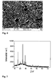
- the bath was then pumped through the cell at 5.4 l / h and heated from 20 ° C to 88 ° C over a period of 120 min by means of additional heating. After completion of the deposition process, the surface of the soda-lime glass is covered with an about 4 .mu.m thick Cu (l) SCN film, as in Fig. 6 shown. According to XRD analysis - s. FIG. 7 All peaks can be assigned to the ⁇ - or ⁇ -CuSCN modification.
- a conductive substrate is used and a CuSCN layer is applied to a 1.0 mm thick aluminum substrate.
- the deposition takes place at a heating temperature of 150 ° C.
- the bath temperature rises from 20 ° C to 100 ° C.
- the hot Al substrate is rinsed with the bath solution for 5 min.
- On the sample grows a microstructure, which consists of large platelet-shaped crystallites (s. Fig. 8 ).
- the XRD analysis of the grown-up layer yields maxima which are attributed to the ⁇ - and - the predominant - ⁇ -CuSCN modification as well as the aluminum of the substrate.
- the bath temperature rises from 20 ° C to 70 ° C at a heating temperature of 160 ° C.
- the sample is lapped for 10 minutes by the bath solution, this process is repeated again.
- the polyimide film is overgrown at the edges with a CuSCN layer of the ⁇ - and ⁇ -CuSCN modifications, but only sporadic crystal growth is observed in the center of the film.
- Fig. 9 shows an SEM image of only the edge region of the sample with a dense growth of a CuSCN layer.
- the exemplary embodiments prove that the method according to the invention, using chemical bath deposition, makes it possible to deposit thin transparent CuSCN layers on different substrates.
Landscapes
- Chemical & Material Sciences (AREA)
- Engineering & Computer Science (AREA)
- Physics & Mathematics (AREA)
- Thermal Sciences (AREA)
- General Chemical & Material Sciences (AREA)
- Chemical Kinetics & Catalysis (AREA)
- Materials Engineering (AREA)
- Mechanical Engineering (AREA)
- Metallurgy (AREA)
- Organic Chemistry (AREA)
- Inorganic Chemistry (AREA)
- Photovoltaic Devices (AREA)
- Chemically Coating (AREA)
Applications Claiming Priority (1)
| Application Number | Priority Date | Filing Date | Title |
|---|---|---|---|
| DE201010033198 DE102010033198B4 (de) | 2010-08-03 | 2010-08-03 | Verfahren zur Herstellung einer nanokristallinen CuSCN-Schicht auf einem Substrat |
Publications (3)
| Publication Number | Publication Date |
|---|---|
| EP2415902A2 true EP2415902A2 (fr) | 2012-02-08 |
| EP2415902A3 EP2415902A3 (fr) | 2012-03-14 |
| EP2415902A8 EP2415902A8 (fr) | 2012-04-04 |
Family
ID=44582029
Family Applications (1)
| Application Number | Title | Priority Date | Filing Date |
|---|---|---|---|
| EP11075187A Withdrawn EP2415902A3 (fr) | 2010-08-03 | 2011-08-02 | Procédé destiné à la fabrication d'une couche de CuSCN nanocristalline sur un substrat |
Country Status (2)
| Country | Link |
|---|---|
| EP (1) | EP2415902A3 (fr) |
| DE (1) | DE102010033198B4 (fr) |
Cited By (1)
| Publication number | Priority date | Publication date | Assignee | Title |
|---|---|---|---|---|
| CN108793197A (zh) * | 2018-03-01 | 2018-11-13 | 复旦大学 | 银掺杂硫氰酸亚铜薄膜及其制备方法和应用 |
Citations (2)
| Publication number | Priority date | Publication date | Assignee | Title |
|---|---|---|---|---|
| WO2000052764A1 (fr) | 1999-02-26 | 2000-09-08 | Hahn-Meitner-Institut Berlin Gmbh | Depot electrochimique de cuscn dans des films tio2 poreux |
| DE10142913A1 (de) | 2001-08-27 | 2003-03-27 | Hahn Meitner Inst Berlin Gmbh | Transistoranordnung und Verfahren zu deren Herstellung |
Family Cites Families (1)
| Publication number | Priority date | Publication date | Assignee | Title |
|---|---|---|---|---|
| CN100552095C (zh) * | 2007-07-27 | 2009-10-21 | 中国科学院上海硅酸盐研究所 | 一种液相条件下制备硫氰酸亚铜薄膜的方法 |
-
2010
- 2010-08-03 DE DE201010033198 patent/DE102010033198B4/de not_active Expired - Fee Related
-
2011
- 2011-08-02 EP EP11075187A patent/EP2415902A3/fr not_active Withdrawn
Patent Citations (2)
| Publication number | Priority date | Publication date | Assignee | Title |
|---|---|---|---|---|
| WO2000052764A1 (fr) | 1999-02-26 | 2000-09-08 | Hahn-Meitner-Institut Berlin Gmbh | Depot electrochimique de cuscn dans des films tio2 poreux |
| DE10142913A1 (de) | 2001-08-27 | 2003-03-27 | Hahn Meitner Inst Berlin Gmbh | Transistoranordnung und Verfahren zu deren Herstellung |
Non-Patent Citations (10)
| Title |
|---|
| ADV. MAT, vol. 17, 2005, pages 1512 - 1515 |
| APPL. PHYS. LETT., vol. 93, 2008, pages 053113 |
| BERICHTE DER DEUTSCHEN CHEMISCHEN GESELLSCHAFT (A AND B SERIES, vol. 69, 1936, pages 1601 - 1610 |
| CHEMISTRY OF MATERIALS, vol. 14, pages 5023 - 5029 |
| ELECTROCHEM. AND SOLID-STATE LETTERS, vol. 12, no. 3, 2009, pages H54 - H57 |
| JOURNAL OF PHYSICS D: APPLIED PHYSICS, vol. 31, 1998, pages 2326 - 2330 |
| JOURNAL OF THE AMERICAN CERAMIC SOCIETY, vol. 90, 2007, pages 2966 - 2973 |
| SOLAR ENERGY MATERIALS & CELLS, vol. 86, 2005, pages 443 - 450 |
| SOLAR ENERGY MATERIALS & SOLAR CELLS, vol. 58, 1999, pages 337 - 347 |
| THIN SOLID FILMS, vol. 451-452, March 2004 (2004-03-01), pages 128 - 132 |
Cited By (2)
| Publication number | Priority date | Publication date | Assignee | Title |
|---|---|---|---|---|
| CN108793197A (zh) * | 2018-03-01 | 2018-11-13 | 复旦大学 | 银掺杂硫氰酸亚铜薄膜及其制备方法和应用 |
| CN108793197B (zh) * | 2018-03-01 | 2021-08-20 | 复旦大学 | 银掺杂硫氰酸亚铜薄膜及其制备方法和应用 |
Also Published As
| Publication number | Publication date |
|---|---|
| DE102010033198B4 (de) | 2013-04-04 |
| EP2415902A8 (fr) | 2012-04-04 |
| DE102010033198A1 (de) | 2012-02-09 |
| EP2415902A3 (fr) | 2012-03-14 |
Similar Documents
| Publication | Publication Date | Title |
|---|---|---|
| EP2051936B1 (fr) | Procédé permettant la production de nanoparticules oxydées à partir d'un matériau qui forme des particules d'oxyde | |
| DE102013109394B4 (de) | Anodische Oxidschicht und Verfahren zur Herstellung derselben | |
| DE69025495T2 (de) | Abscheidung von Silberschichten auf nichtleitenden Substraten | |
| EP2398934B1 (fr) | Procede pour la fabrication des cuoches d'oxyde d'indium semiconducteurs, articles obtenues et utilisation de cettes couches | |
| DE102007010872A1 (de) | Verfahren zur Präzisionsbearbeitung von Substraten und dessen Verwendung | |
| DE69231779T2 (de) | Herstellungsverfahren von ohmschen Kontakten und photovoltaische Zelle mit ohmschem Kontakt | |
| EP1792348B1 (fr) | Procede pour appliquer une couche tampon de sulfure de zinc sur un substrat semiconducteur par depot en bain chimique, en particulier sur la couche absorbante d'une cellule solaire en couches minces a base de chalcopyrite | |
| EP3053186A1 (fr) | Dispositif et procédé de production en continu de couches de silicium poreuses | |
| WO2009006988A1 (fr) | Structure de contact pour un composant semi-conducteur et son procédé de fabrication | |
| EP2252728A2 (fr) | Procédé d'électrodéposition pour la production de zno nanostructuré | |
| WO2011092236A2 (fr) | Solution de dépôt en bain chimique pour dépôt chimique par voie humide d'une couche de sulfure métallique et procédé de production associé | |
| WO2001086029A1 (fr) | Couches formees par voie electrochimique et servant de protection anticorrosion ou de peinture primaire reactive | |
| WO2004023529A2 (fr) | Procede et dispositif pour traiter thermiquement des plaquettes semi-conductrices | |
| DE102010033198B4 (de) | Verfahren zur Herstellung einer nanokristallinen CuSCN-Schicht auf einem Substrat | |
| DE102018203256A1 (de) | Verfahren zum Einbringen eines photovoltaisch aktiven Materials in ein eine Vielzahl von Zellen aufweisendes photovoltaisches Modul und entsprechendes photovoltaisches Modul | |
| EP2411558B1 (fr) | Procédé pour appliquer une couche tampon de zn(s, o) sur un substrat semi-conducteur par dépôt par bain chimique | |
| DE102010030884A1 (de) | Verfahren zur Abscheidung einer Pufferschicht auf einer CIS-Dünnschicht-Solarzelle und nach dem Verfahren hergestellte CIS-Dünnschicht-Solarzelle | |
| DE102020113518B4 (de) | Verfahren zur Herstellung einer Schicht aus Bismutvanadat | |
| DE10330192A1 (de) | Elektrisch leitender Körper mit einer Haftvermittlungsschicht sowie Verfahren zum Abscheiden einer Haftvermittlungsschicht | |
| DE102012023349B4 (de) | Verfahren und Vorrichtung zur strukturierten Beschichtung der Innenseite eines Schlauchs oder Rohrs | |
| DE102008037177B4 (de) | Verfahren zur Herstellung nanostrukturierter Metalloxide oder -chalkogenide mittels chemischer Badabscheidung | |
| DE102007006455B4 (de) | Wärmereservoir und Verfahren zur Bearbeitung eines mit einem Wärmereservoir thermisch gekoppelten Substrates sowie Verwendung eines Wärmetransportmediums | |
| WO2022253385A1 (fr) | Procédé de fabrication d'absorbeurs à large bande à positionnement très précis pour surfaces 2d et 3d | |
| EP1448808B1 (fr) | Procede de fabrication de revetements fins peu solubles | |
| AT515522B1 (de) | Verfahren zur elektrochemischen abscheidung halbleitender materialien und elektrolyten hierzu |
Legal Events
| Date | Code | Title | Description |
|---|---|---|---|
| AK | Designated contracting states |
Kind code of ref document: A2 Designated state(s): AL AT BE BG CH CY CZ DE DK EE ES FI FR GB GR HR HU IE IS IT LI LT LU LV MC MK MT NL NO PL PT RO RS SE SI SK SM TR |
|
| AX | Request for extension of the european patent |
Extension state: BA ME |
|
| PUAI | Public reference made under article 153(3) epc to a published international application that has entered the european phase |
Free format text: ORIGINAL CODE: 0009012 |
|
| PUAL | Search report despatched |
Free format text: ORIGINAL CODE: 0009013 |
|
| AK | Designated contracting states |
Kind code of ref document: A3 Designated state(s): AL AT BE BG CH CY CZ DE DK EE ES FI FR GB GR HR HU IE IS IT LI LT LU LV MC MK MT NL NO PL PT RO RS SE SI SK SM TR |
|
| AX | Request for extension of the european patent |
Extension state: BA ME |
|
| RIC1 | Information provided on ipc code assigned before grant |
Ipc: C23C 18/12 20060101AFI20120209BHEP |
|
| 17P | Request for examination filed |
Effective date: 20120914 |
|
| RIC1 | Information provided on ipc code assigned before grant |
Ipc: C23C 18/04 20060101ALI20130129BHEP Ipc: C23C 18/12 20060101AFI20130129BHEP |
|
| GRAP | Despatch of communication of intention to grant a patent |
Free format text: ORIGINAL CODE: EPIDOSNIGR1 |
|
| INTG | Intention to grant announced |
Effective date: 20130627 |
|
| STAA | Information on the status of an ep patent application or granted ep patent |
Free format text: STATUS: THE APPLICATION IS DEEMED TO BE WITHDRAWN |
|
| 18D | Application deemed to be withdrawn |
Effective date: 20131108 |