EP2413348A1 - Semiconductor substrate, semiconductor device, and method of producing semiconductor substrate - Google Patents
Semiconductor substrate, semiconductor device, and method of producing semiconductor substrate Download PDFInfo
- Publication number
- EP2413348A1 EP2413348A1 EP10755694A EP10755694A EP2413348A1 EP 2413348 A1 EP2413348 A1 EP 2413348A1 EP 10755694 A EP10755694 A EP 10755694A EP 10755694 A EP10755694 A EP 10755694A EP 2413348 A1 EP2413348 A1 EP 2413348A1
- Authority
- EP
- European Patent Office
- Prior art keywords
- epitaxial layer
- forming step
- semiconductor substrate
- dopant gas
- conductivity type
- Prior art date
- Legal status (The legal status is an assumption and is not a legal conclusion. Google has not performed a legal analysis and makes no representation as to the accuracy of the status listed.)
- Granted
Links
Images


Classifications
-
- H—ELECTRICITY
- H10—SEMICONDUCTOR DEVICES; ELECTRIC SOLID-STATE DEVICES NOT OTHERWISE PROVIDED FOR
- H10D—INORGANIC ELECTRIC SEMICONDUCTOR DEVICES
- H10D30/00—Field-effect transistors [FET]
- H10D30/60—Insulated-gate field-effect transistors [IGFET]
- H10D30/64—Double-diffused metal-oxide semiconductor [DMOS] FETs
- H10D30/66—Vertical DMOS [VDMOS] FETs
- H10D30/668—Vertical DMOS [VDMOS] FETs having trench gate electrodes, e.g. UMOS transistors
-
- H—ELECTRICITY
- H10—SEMICONDUCTOR DEVICES; ELECTRIC SOLID-STATE DEVICES NOT OTHERWISE PROVIDED FOR
- H10D—INORGANIC ELECTRIC SEMICONDUCTOR DEVICES
- H10D30/00—Field-effect transistors [FET]
- H10D30/01—Manufacture or treatment
- H10D30/021—Manufacture or treatment of FETs having insulated gates [IGFET]
- H10D30/028—Manufacture or treatment of FETs having insulated gates [IGFET] of double-diffused metal oxide semiconductor [DMOS] FETs
- H10D30/0291—Manufacture or treatment of FETs having insulated gates [IGFET] of double-diffused metal oxide semiconductor [DMOS] FETs of vertical DMOS [VDMOS] FETs
- H10D30/0297—Manufacture or treatment of FETs having insulated gates [IGFET] of double-diffused metal oxide semiconductor [DMOS] FETs of vertical DMOS [VDMOS] FETs using recessing of the gate electrodes, e.g. to form trench gate electrodes
-
- H—ELECTRICITY
- H10—SEMICONDUCTOR DEVICES; ELECTRIC SOLID-STATE DEVICES NOT OTHERWISE PROVIDED FOR
- H10D—INORGANIC ELECTRIC SEMICONDUCTOR DEVICES
- H10D62/00—Semiconductor bodies, or regions thereof, of devices having potential barriers
- H10D62/01—Manufacture or treatment
- H10D62/051—Forming charge compensation regions, e.g. superjunctions
- H10D62/058—Forming charge compensation regions, e.g. superjunctions by using trenches, e.g. implanting into sidewalls of trenches or refilling trenches
-
- H—ELECTRICITY
- H10—SEMICONDUCTOR DEVICES; ELECTRIC SOLID-STATE DEVICES NOT OTHERWISE PROVIDED FOR
- H10D—INORGANIC ELECTRIC SEMICONDUCTOR DEVICES
- H10D62/00—Semiconductor bodies, or regions thereof, of devices having potential barriers
- H10D62/10—Shapes, relative sizes or dispositions of the regions of the semiconductor bodies; Shapes of the semiconductor bodies
- H10D62/102—Constructional design considerations for preventing surface leakage or controlling electric field concentration
- H10D62/103—Constructional design considerations for preventing surface leakage or controlling electric field concentration for increasing or controlling the breakdown voltage of reverse-biased devices
- H10D62/105—Constructional design considerations for preventing surface leakage or controlling electric field concentration for increasing or controlling the breakdown voltage of reverse-biased devices by having particular doping profiles, shapes or arrangements of PN junctions; by having supplementary regions, e.g. junction termination extension [JTE]
- H10D62/109—Reduced surface field [RESURF] PN junction structures
- H10D62/111—Multiple RESURF structures, e.g. double RESURF or 3D-RESURF structures
-
- H—ELECTRICITY
- H10—SEMICONDUCTOR DEVICES; ELECTRIC SOLID-STATE DEVICES NOT OTHERWISE PROVIDED FOR
- H10P—GENERIC PROCESSES OR APPARATUS FOR THE MANUFACTURE OR TREATMENT OF DEVICES COVERED BY CLASS H10
- H10P14/00—Formation of materials, e.g. in the shape of layers or pillars
- H10P14/20—Formation of materials, e.g. in the shape of layers or pillars of semiconductor materials
- H10P14/24—Formation of materials, e.g. in the shape of layers or pillars of semiconductor materials using chemical vapour deposition [CVD]
-
- H—ELECTRICITY
- H10—SEMICONDUCTOR DEVICES; ELECTRIC SOLID-STATE DEVICES NOT OTHERWISE PROVIDED FOR
- H10P—GENERIC PROCESSES OR APPARATUS FOR THE MANUFACTURE OR TREATMENT OF DEVICES COVERED BY CLASS H10
- H10P14/00—Formation of materials, e.g. in the shape of layers or pillars
- H10P14/20—Formation of materials, e.g. in the shape of layers or pillars of semiconductor materials
- H10P14/29—Formation of materials, e.g. in the shape of layers or pillars of semiconductor materials characterised by the substrates
- H10P14/2901—Materials
- H10P14/2902—Materials being Group IVA materials
- H10P14/2905—Silicon, silicon germanium or germanium
-
- H—ELECTRICITY
- H10—SEMICONDUCTOR DEVICES; ELECTRIC SOLID-STATE DEVICES NOT OTHERWISE PROVIDED FOR
- H10P—GENERIC PROCESSES OR APPARATUS FOR THE MANUFACTURE OR TREATMENT OF DEVICES COVERED BY CLASS H10
- H10P14/00—Formation of materials, e.g. in the shape of layers or pillars
- H10P14/20—Formation of materials, e.g. in the shape of layers or pillars of semiconductor materials
- H10P14/32—Formation of materials, e.g. in the shape of layers or pillars of semiconductor materials characterised by intermediate layers between substrates and deposited layers
- H10P14/3242—Structure
-
- H—ELECTRICITY
- H10—SEMICONDUCTOR DEVICES; ELECTRIC SOLID-STATE DEVICES NOT OTHERWISE PROVIDED FOR
- H10P—GENERIC PROCESSES OR APPARATUS FOR THE MANUFACTURE OR TREATMENT OF DEVICES COVERED BY CLASS H10
- H10P14/00—Formation of materials, e.g. in the shape of layers or pillars
- H10P14/20—Formation of materials, e.g. in the shape of layers or pillars of semiconductor materials
- H10P14/34—Deposited materials, e.g. layers
- H10P14/3402—Deposited materials, e.g. layers characterised by the chemical composition
- H10P14/3404—Deposited materials, e.g. layers characterised by the chemical composition being Group IVA materials
- H10P14/3411—Silicon, silicon germanium or germanium
-
- H—ELECTRICITY
- H10—SEMICONDUCTOR DEVICES; ELECTRIC SOLID-STATE DEVICES NOT OTHERWISE PROVIDED FOR
- H10P—GENERIC PROCESSES OR APPARATUS FOR THE MANUFACTURE OR TREATMENT OF DEVICES COVERED BY CLASS H10
- H10P14/00—Formation of materials, e.g. in the shape of layers or pillars
- H10P14/20—Formation of materials, e.g. in the shape of layers or pillars of semiconductor materials
- H10P14/34—Deposited materials, e.g. layers
- H10P14/3438—Doping during depositing
- H10P14/3441—Conductivity type
- H10P14/3442—N-type
-
- H—ELECTRICITY
- H10—SEMICONDUCTOR DEVICES; ELECTRIC SOLID-STATE DEVICES NOT OTHERWISE PROVIDED FOR
- H10P—GENERIC PROCESSES OR APPARATUS FOR THE MANUFACTURE OR TREATMENT OF DEVICES COVERED BY CLASS H10
- H10P14/00—Formation of materials, e.g. in the shape of layers or pillars
- H10P14/20—Formation of materials, e.g. in the shape of layers or pillars of semiconductor materials
- H10P14/34—Deposited materials, e.g. layers
- H10P14/3438—Doping during depositing
- H10P14/3441—Conductivity type
- H10P14/3444—P-type
-
- H—ELECTRICITY
- H10—SEMICONDUCTOR DEVICES; ELECTRIC SOLID-STATE DEVICES NOT OTHERWISE PROVIDED FOR
- H10D—INORGANIC ELECTRIC SEMICONDUCTOR DEVICES
- H10D62/00—Semiconductor bodies, or regions thereof, of devices having potential barriers
- H10D62/10—Shapes, relative sizes or dispositions of the regions of the semiconductor bodies; Shapes of the semiconductor bodies
- H10D62/17—Semiconductor regions connected to electrodes not carrying current to be rectified, amplified or switched, e.g. channel regions
- H10D62/393—Body regions of DMOS transistors or IGBTs
Definitions
- the present invention relates to a semiconductor substrate, a semiconductor device and a method of producing a semiconductor substrate.
- a power MOSFET Metal Oxide Semiconductor Field Effect Transistor
- a super junction structure can be exemplified.
- an n-type layer and a p-type layer are alternately formed in a conductive layer that connects a source and a drain.
- a depletion layer is formed in an interface between the n-type layer and the p-type layer. Accordingly, between the source and the drain, an electric field is formed not only in a direction from the source to the drain, but also in a direction from the n-type layer to the p-type layer. As a result, the electric field between the source and the drain does not concentrate on a certain part in the conductive layer. Therefore, the super junction structure can provide high voltage resistance performance.
- the present invention is aimed at providing a semiconductor substrate, a semiconductor device and a method of producing a semiconductor substrate that are more likely to provide desired electrical characteristics.
- a method of producing a semiconductor substrate includes: a first epitaxial layer forming step of forming a first epitaxial layer by introducing a dopant gas of a first conductivity type to a semiconductor substrate of the first conductivity type; a trench forming step of forming a trench in the first epitaxial layer; and an epitaxial layer forming step of forming an epitaxial layer of a second conductivity type that is different from the first conductivity type on the first epitaxial layer and in the trench so as to fill up the trench, using a plurality of growth conditions including different growth rates, and making concentration of a dopant gas of the second conductivity type, which is incorporated into the epitaxial layer, constant in each of the plurality of growth conditions.
- the plurality of growth conditions includes growth temperature of the epitaxial layer; and the growth rate is changed by changing the growth temperature of the epitaxial layer.
- the plurality of growth conditions includes flow rate of the dopant gas of the second conductivity type that is introduced into the epitaxial layer and the trench; and the growth rate is changed by changing the flow rate of a material gas.
- a method of producing a semiconductor substrate includes: a first epitaxial layer forming step of forming a first epitaxial layer by introducing a dopant gas of a first conductivity type to a semiconductor substrate of the first conductivity type; a trench forming step of forming a trench in the first epitaxial layer; and a second epitaxial layer forming step of forming a second epitaxial layer on the first epitaxial layer and in the trench, by introducing a dopant gas of a second conductivity type that is different from the first conductivity type at a predetermined first dopant gas flow rate, in an atmosphere of a predetermined first temperature; a third epitaxial layer forming step of forming a third epitaxial layer to fill up the trench, by introducing the dopant gas of the second conductivity type to the second epitaxial layer at a second dopant gas flow rate that is greater than the first dopant gas flow rate, in an atmosphere of a second temperature that is lower than the
- a method of producing a semiconductor substrate includes: a first epitaxial layer forming step of forming a first epitaxial layer by introducing a dopant gas of a first conductivity type to a semiconductor substrate of the first conductivity type; a trench forming step of forming a trench in the first epitaxial layer; and a second epitaxial layer forming step of forming a second epitaxial layer on the first epitaxial layer and in the trench, by introducing a dopant gas of a second conductivity type that is different from the first conductivity type at a predetermined first dopant gas flow rate, in an atmosphere of a predetermined first temperature; and a third epitaxial layer forming step of forming a third epitaxial layer to fill up the trench, by introducing the dopant gas of the second conductivity type to the second epitaxial layer at a second dopant gas flow rate that is greater than the first dopant gas flow rate, in an atmosphere of a second temperature that is lower than the
- a method of producing a semiconductor substrate includes: a first epitaxial layer forming step of forming a first epitaxial layer by introducing a dopant gas of a first conductivity type to a semiconductor substrate of the first conductivity type; a trench forming step of forming a trench in the first epitaxial layer; a second epitaxial layer forming step of forming a second epitaxial layer on the first epitaxial layer and in the trench, by introducing a dopant gas of a second conductivity type that is different from the first conductivity type at a predetermined first dopant gas flow rate, in an atmosphere of a predetermined first temperature; and a third epitaxial layer forming step of forming a third epitaxial layer to fill up the trench, by introducing the dopant gas of the second conductivity type to the second epitaxial layer at a second dopant gas flow rate that is greater than the first dopant gas flow rate, in an atmosphere of a second temperature that is higher than the first
- a seventh aspect of the present invention in the method of producing a semiconductor substrate as described in the fourth aspect, it is preferable that amount of dopant in the second epitaxial layer, the third epitaxial layer, and the fourth epitaxial layer is changed by changing the flow rate of the dopant gas of the second conductivity type.
- the method of producing a semiconductor substrate as described in the fourth aspect it is preferable that amount of dopant in the second epitaxial layer, the third epitaxial layer, and the fourth epitaxial layer is changed by using a plurality of gas cylinders of different concentrations of the dopant gas of the second conductivity type.
- the method of producing a semiconductor substrate as described in the fourth aspect it is preferable that at least one of the second epitaxial layer, the third epitaxial layer and the fourth epitaxial layer is formed by feeding a material gas and a halide gas in parallel in the atmosphere.
- amount of dopant is substantially the same in the second epitaxial layer, the third epitaxial layer and the fourth epitaxial layer.
- a flow rate of a halide gas in the atmosphere is greater in the third epitaxial layer forming step than in the second epitaxial layer forming step and the fourth epitaxial layer forming step.
- a semiconductor substrate is manufactured by the method of producing a semiconductor substrate as described in the first aspect.
- a semiconductor device uses the semiconductor substrate as described in the twelfth aspect.
- the present invention is aimed at providing a semiconductor substrate, a semiconductor device and a method of producing a semiconductor substrate that are more likely to provide desired electrical characteristics.
- FIG. 1 is a partial cross-sectional view schematically showing an embodiment of a semiconductor substrate according to the present invention.
- a first epitaxial layer 11 is formed on a silicon substrate 10 and a plurality of trenches 12 is formed in the first epitaxial layer 11.
- a second epitaxial layer 13 is sequentially formed in the trenches 12, a second epitaxial layer 13, the third epitaxial layer 14 and a fourth epitaxial layer 15 are sequentially formed.
- the fourth epitaxial layer 15 is formed also on the first epitaxial layer 11.
- the silicon substrate 10 is an n+ type silicon substrate to which an n-type dopant is introduced to single crystal silicon at a high concentration.
- the first epitaxial layer 11 is formed on the silicon substrate 10.
- the first epitaxial layer 11 is an n-type silicon epitaxial layer to which an n-type dopant is introduced at a lower concentration than in the silicon substrate 10.
- the plurality of trenches 12 is formed in the first epitaxial layer 11.
- a bottom face of the trenches 12 is a main surface of the silicon substrate 10.
- the trenches 12 are substantially in a rectangular pole shape.
- a side face of the trenches 12 is an inner side face of the first epitaxial layer 11.
- the second epitaxial layer 13 is formed on a main surface of the first epitaxial layer 11 and in the trenches 12.
- the second epitaxial layer 13 is a p-type silicon epitaxial layer to which a p-type dopant is introduced.
- the third epitaxial layer 14 is formed on the second epitaxial layer 13.
- the third epitaxial layer 14 is a p-type silicon epitaxial layer to which a p-type dopant is introduced.
- the second epitaxial layer 13 and the third epitaxial layer 14 fill up almost an entirety of the trenches 12 except for a part thereof.
- the fourth epitaxial layer 15 is formed on a main surface of the second epitaxial layer 13 and a main surface of the third epitaxial layer 14 that are formed on the main surface of the first epitaxial layer 11, as well as in the part of the trenches 12 that has not been filled.
- the fourth epitaxial layer 15 is a p-type silicon epitaxial layer to which a p-type dopant is introduced.
- the first epitaxial layer 11 is composed of an n-type epitaxial layer to which a dopant such as P (phosphorus), As (arsenic), Sb (antimony) and the like is introduced.
- the second epitaxial layer 13, the third epitaxial layer 14, and the fourth epitaxial layer 15 are composed of a p-type epitaxial layer to which a dopant such as B (boron), Ga (gallium) and In (indium) is introduced.
- a conductivity type of the second epitaxial layer 13, the third epitaxial layer 14 and the fourth epitaxial layer 15 is different from that of the first epitaxial layer 11.
- a conductivity type that is different is p-type for n-type, or n-type for p-type. Therefore, for example, if a conductivity type of the first epitaxial layer 11 is n-type, a conductivity type of the second epitaxial layer 13, the third epitaxial layer 14 and the fourth epitaxial layer 15 is p-type.
- the semiconductor substrate 1 has a super junction structure in which the first epitaxial layer 11 that is n-type, the second epitaxial layer 13, the third epitaxial layer 14, and the fourth epitaxial layer 15 that are p-type are formed alternately on the silicon substrate 10.
- amount of dopant included in the first epitaxial layer 11 and amount of dopant included in the second epitaxial layer 13, the third epitaxial layer 14 and the fourth epitaxial layer 15 are substantially the same.
- a p-n junction between: the first epitaxial layer 11 that is n-type; and the second epitaxial layer 13, the third epitaxial layer 14, and the fourth epitaxial layer 15 that are p-type provides a depletion layer to fully deplete a drift region, thereby maintaining high voltage resistance performance.
- FIG. 2 is a flow chart showing an embodiment of a method of producing the semiconductor substrate according to the present invention.
- FIGS. 3A to 3E are partial cross-sectional views sequentially showing changes in the semiconductor substrate 1 in the method of producing a semiconductor substrate shown in FIG. 2 .
- the method of producing a semiconductor substrate according to the present embodiment includes: a first epitaxial layer forming step S1; a trench forming step S2; a second epitaxial layer forming step S3; a third epitaxial layer forming step S4; and a fourth epitaxial layer forming step S5.
- a first epitaxial layer forming step S1 a trench forming step S2
- a second epitaxial layer forming step S3 a third epitaxial layer forming step S4
- Each step (S1 to S5) is described hereinafter, with reference to FIG. 3 as necessary.
- an n-type dopant gas is supplied while supplying a material gas to the silicon substrate 10 of n+ type, thereby forming the first epitaxial layer 11 in an atmosphere containing the material gas and the dopant gas.
- SiH 4 monosilane
- Si 2 H 6 diisilane
- SiH 2 Cl 2 diichlorosilane
- SiHCl 3 trichlorosilane
- SiCl 4 sicon tetrachloride
- phosphine (PH 3 ) that contain phosphorus (P) and arsine (AsH 3 ) that contain arsenic (As), which are n-type dopants
- phosphine (PH 3 ) that contain phosphorus (P)
- arsine (AsH 3 ) that contain arsenic (As)
- B 2 H 6 diborane
- BCl 3 boron trichloride
- B boron trichloride
- the abovementioned gases can be used similarly in the second epitaxial layer forming step S3, the third epitaxial layer forming step S4 and the fourth epitaxial layer forming step S5 that are described later.
- a method for forming the first epitaxial layer 11, the second epitaxial layer 13, the third epitaxial layer 14 and the fourth epitaxial layer 15 is not particularly limited, chemical vapor deposition (CVD), physical vapor deposition (PVD), molecular beam epitaxy (MBE) and the like are preferably used.
- CVD chemical vapor deposition
- PVD physical vapor deposition
- MBE molecular beam epitaxy
- a resist pattern is formed by photolithography at a predetermined position on the first epitaxial layer 11 formed in the first epitaxial layer forming step S1. And then, a region in which the resist pattern is not formed on the first epitaxial layer 11 is etched by, for example, reactive ion etching, thereby forming the trenches 12. Thereafter, the trenches 12 shown in FIG. 3B are obtained by removing the resist pattern.
- a p-type dopant gas is introduced to the first epitaxial layer 11 and the trenches 12, while supplying the material gas and the halide gas thereto, thereby forming the second epitaxial layer 13 in an atmosphere containing the material gas, the halide gas, and the dopant gas.
- a temperature of the atmosphere containing the material gas, the halide gas, and the dopant gas is preferably 950 to 1000°C (predetermined first temperature), and a flow rate of the dopant gas (predetermined first dopant gas flow rate) is preferably 100 to 300 sccm (Standard Cubic Centimeter per Minute).
- an amount of dopant in the second epitaxial layer 13 is preferably 1 ⁇ 10 15 to 1 ⁇ 10 17 (cm -3 ).
- the dopant amount is a value defined, before incorporation of a dopant gas by an epitaxial layer, by a flow rate and concentration of the dopant gas; and, after incorporation of the dopant gas by the epitaxial layer, defined by a density of dopant atoms in a crystal lattice of the epitaxial layer.
- halide gas HCl (hydrogen chloride), Cl 2 (chlorine), F 2 (fluorine), CLF 3 (chlorine trifluoride), HF (hydrogen fluoride), HBr (hydrogen bromide) and the like can be exemplified.
- the halide gas the abovementioned gases can be used similarly in the third epitaxial layer forming step S4 and the fourth epitaxial layer forming step S5 that are described later.
- the halide gas functions as an etching gas inside the trenches 12. Since an etching rate of the halide gas is slower in a bottom part of the trenches 12 than in an opening part of the trenches 12, a formation rate of an epitaxial layer is faster in the bottom part than in the opening part of the trenches 12. Generation of a void in the second epitaxial layer 13 formed in the trenches 12 can thus be prevented.
- a p-type dopant gas is introduced to the second epitaxial layer 13, while supplying the material gas and the halide gas thereto, thereby forming the third epitaxial layer 14 to fill up the trenches 12, in an atmosphere containing the material gas, the halide gas, and the dopant gas.
- the third epitaxial layer 14 is formed also in a region on the second epitaxial layer 13, outside of the trenches 12.
- a temperature of the atmosphere containing the material gas, the halide gas, and the dopant gas is 900 to 950°C (second temperature), which is lower than that in the second epitaxial layer forming step S3.
- a flow rate of the p-type dopant gas (second dopant gas flow rate), is 110 to 360 sccm, which is higher than that in the second epitaxial layer forming step S3.
- an amount of dopant in the third epitaxial layer 14 (second dopant amount) is preferably 1 ⁇ 10 15 to 1 ⁇ 10 17 (cm -3 ).
- a difference between the temperature of the atmosphere in the second epitaxial layer forming step S3 and the temperature of the atmosphere in the third epitaxial layer forming step S4 is preferably at least 10°C, and more preferably at least 50°C.
- a difference between the flow rate of the p-type dopant gas in the second epitaxial layer forming step S3 and the flow rate of the p-type dopant gas in the third epitaxial layer forming step S4 is preferably at least 5 sccm, and more preferably at least 30 sccm.
- the second epitaxial layer 13 and the third epitaxial layer 14 fill up almost an entirety of the trenches 12 except for a part thereof.
- a temperature of the atmosphere in the third epitaxial layer forming step S4 is lower than that in the second epitaxial layer forming step S3. Generation of a void and crystal defect in the third epitaxial layer 14 can thus be prevented.
- a p-type dopant gas is introduced to the second epitaxial layer 13 and the third epitaxial layer 14, while supplying the material gas and the halide gas thereto, thereby forming the fourth epitaxial layer 15 in an atmosphere containing the material gas, the halide gas, and the dopant gas.
- a temperature of the atmosphere containing the material gas, the halide gas, and the dopant gas is 950 to 1000°C (third temperature), which is higher than that in the third epitaxial layer forming step S4.
- a flow rate of the p-type dopant gas (third dopant gas flow rate), is 100 to 300 sccm, which is lower than that in the third epitaxial layer forming step S4.
- an amount of dopant in the fourth epitaxial layer 15 (third dopant amount) is preferably 1 ⁇ 10 15 to 1 ⁇ 10 17 (cm -3 ) .
- a difference between the temperature of the atmosphere in the fourth epitaxial layer forming step S5 and the temperature of the atmosphere in the third epitaxial layer forming step S4 is preferably at least 10°C, and more preferably at least 50°C.
- a difference between the flow rate of the p-type dopant gas in the fourth epitaxial layer forming step S5 and the flow rate of the p-type dopant gas in the third epitaxial layer forming step S4 is preferably at least 5 sccm, and more preferably at least 30 sccm.
- a conductivity type of the silicon substrate 10 and the first epitaxial layer 11 is n-type
- a conductivity type of the second epitaxial layer 13, the third epitaxial layer 14 and the fourth epitaxial layer 15 is p-type
- the present invention is not limited thereto.
- the conductivity type of the silicon substrate 10 and the first epitaxial layer 11 can be p-type
- the conductivity type of the second epitaxial layer 13, the third epitaxial layer 14 and the fourth epitaxial layer 15 can be n-type.
- a flow rate of the n-type dopant gas in the third epitaxial layer forming step S4 is lower than that in the second epitaxial layer forming step S3.
- a flow rate of the n-type dopant gas in the fourth epitaxial layer forming step S5 is lower than that in the third epitaxial layer forming step S4.
- the second epitaxial layer 13, the third epitaxial layer 14 and the fourth epitaxial layer 15 are formed on the first epitaxial layer 11 and the trenches 12 to fill up the trenches 12, using a plurality of growth conditions including different growth rates.
- concentration of the p-type dopant incorporated into the second epitaxial layer 13, the third epitaxial layer 14 and the fourth epitaxial layer 15 is constant.
- the plurality of growth conditions includes growth temperature of the second epitaxial layer 13, the third epitaxial layer 14 and the fourth epitaxial layer 15.
- the abovementioned growth rate is changed by changing the growth temperature of the second epitaxial layer 13, the third epitaxial layer 14 and the fourth epitaxial layer 15.
- the plurality of growth conditions can include a flow rate of the p-type dopant gas incorporated into the trenches 12, the second epitaxial layer 13, the third epitaxial layer 14 and the fourth epitaxial layer 15.
- the growth rate is changed by changing the flow rate of the material gas (silicon source gas).
- a temperature of the atmosphere in the second epitaxial layer forming step S3 and the fourth epitaxial layer forming step S5 (approximately 950 to 1000°C) is higher than that in the third epitaxial layer forming step S4 (approximately 900 to 950°C).
- a formation rate of the second epitaxial layer 13 and the fourth epitaxial layer 15 can be increased and throughput can be improved.
- a temperature of the atmosphere in the second epitaxial layer forming step S3 and the fourth epitaxial layer forming step S5 (approximately 950 to 1000°C) is higher than that in the third epitaxial layer forming step S4 (approximately 900 to 950°C)
- dopant concentration in the third epitaxial layer 14 tends to be lower than that of the second epitaxial layer 13 and the fourth epitaxial layer 15.
- a flow rate of the dopant gas in the third epitaxial layer forming step S4 is set to be lower than that in the second epitaxial layer forming step S3 and the fourth epitaxial layer forming step S5.
- At least one of the second epitaxial layer 13, the third epitaxial layer 14 and the fourth epitaxial layer 15 is preferably formed by feeding a material gas and a halide gas in parallel in the atmosphere. More specifically, for example the second epitaxial layer 13 and the third epitaxial layer 14 are formed by feeding a material gas and a halide gas in parallel in the atmosphere of the second epitaxial layer forming step S3 and the third epitaxial layer forming step S4.
- the flow rate of the halide gas in the atmosphere is preferably greater in the third epitaxial layer forming step S4 than in the second epitaxial layer forming step S3 and the fourth epitaxial layer forming step S5.
- the dopant concentration or the dopant amount of the second epitaxial layer 13, the third epitaxial layer 14 and the fourth epitaxial layer 15 is preferably substantially the same.
- the dopant concentration being substantially the same means that a difference in the dopant amount is no greater than ⁇ 5%.
- the method of producing a semiconductor substrate according to the present embodiment is provided with: the first epitaxial layer forming step S1 of forming the first epitaxial layer 11; the trench forming step S2 of forming the trenches in the first epitaxial layer; the second epitaxial layer forming step S3 of forming the second epitaxial layer on the first epitaxial layer 11 and inside the trenches 12; the third epitaxial layer forming step S4 of forming the third epitaxial layer 14 on the second epitaxial layer 13; and the fourth epitaxial layer forming step S5 of forming the fourth epitaxial layer on the second epitaxial layer and the third epitaxial layer.
- a temperature of the atmosphere in the second epitaxial layer forming step S3 and the fourth epitaxial layer forming step S5 is higher than that in the third epitaxial layer forming step S4, and a flow rate of the dopant gas in the third epitaxial layer forming step S4 is higher than in the second epitaxial layer forming step S3 and the fourth epitaxial layer forming step S5.
- the dopant concentration of the second epitaxial layer 13, the third epitaxial layer 14, and the fourth epitaxial layer 15 can be made substantially the same, in resistivity measurement of the semiconductor substrate 1, for example, resistivity of the second epitaxial layer 13, the third epitaxial layer 14; and the fourth epitaxial layer 15 is substantially the same.
- the method of producing a semiconductor substrate of the present embodiment can provide desired electrical characteristics. Therefore, a power MOSFET that is manufactured using the semiconductor substrate 1 including the second epitaxial layer 13, the third epitaxial layer 14, and the fourth epitaxial layer 15 of the present embodiment (see FIG. 4 or 5 ) can provide desired electrical characteristics such as high voltage resistance performance and on resistance.
- the method of producing a semiconductor substrate can provide the same effect even if a flow rate of at least one of the material gas and the halide gas is changed.
- the growth temperature is changed in three levels in the second epitaxial layer forming step S3, the third epitaxial layer forming step S4 and the fourth epitaxial layer forming step S5; however, the present invention is not limited thereto.
- the growth temperature of the epitaxial layer inside the trenches 12 can be changed in two levels, for example.
- the growth temperature of the epitaxial layer can be changed from approximately 950 to 1000°C to approximately 900 to 950°C, or from approximately 900 to 950°C to approximately 950 to 1000°C.
- the method of producing a semiconductor substrate according to the present invention can include: the first epitaxial layer forming step S1 the trench forming step S2; the second epitaxial layer forming step S3; and the third epitaxial layer forming step S4.
- the second epitaxial layer 13 of p-type is formed by introducing a p-type dopant gas to the first epitaxial layer 11 and the trenches 12 of n-type, at the first dopant gas flow rate, in an atmosphere of approximately 950 to 1000°C.
- the third epitaxial layer 14 of p-type is formed to fill up the trenches 12, by introducing a p-type dopant gas to the second epitaxial layer 13, at the second dopant gas flow rate that is higher than the first dopant gas flow rate, in an atmosphere of approximately 900 to 950°C.
- the second epitaxial layer 13 is formed by introducing an n-type dopant gas to the first epitaxial layer 11 and the trenches 12, at the first dopant gas flow rate, in an atmosphere of approximately 950 to 1000°C.
- the third epitaxial layer 14 of n-type is formed to fill up the trenches 12, by introducing an n-type dopant gas at the second dopant gas flow rate that is lower than the first dopant gas flow rate, in an atmosphere of approximately 900 to 950°C.
- the second epitaxial layer 13 is formed in an atmosphere of approximately 950 to 1000°C.
- the third epitaxial layer 14 is formed in an atmosphere of approximately 900 to 950°C, a growth temperature lower than that of the second epitaxial layer 13.
- the fourth epitaxial layer 15 is not formed and the second epitaxial layer 13 and the third epitaxial layer 14 are formed to fill up the trenches 12.
- the second epitaxial layer 13 can be formed by introducing a p-type dopant gas to the first epitaxial layer 11 and the trenches 12, at the first dopant gas flow rate, in an atmosphere of approximately 900 to 950°C.
- the third epitaxial layer 14 can be formed to fill up the trenches 12, by introducing a p-type dopant gas to the second epitaxial layer 13, at the second dopant gas flow rate that is higher than the first dopant gas flow rate, in an atmosphere of approximately 950 to 1000°C.
- the fourth epitaxial layer 15 is not formed and the second epitaxial layer 13 and the third epitaxial layer 14 are formed to fill up the trenches 12.
- the second epitaxial layer 13 can be formed by introducing an n-type dopant gas to the first epitaxial layer 11 and the trenches 12, at the first dopant gas flow rate, in an atmosphere of approximately 900 to 950°C.
- the third epitaxial layer 14 can be formed to fill up the trenches 12, by introducing an n-type dopant gas at the second dopant gas flow rate that is lower than the first dopant gas flow rate, in an atmosphere of approximately 950 to 1000°C.
- the fourth epitaxial layer 15 is not formed and the second epitaxial layer 13 and the third epitaxial layer 14 are formed to fill up the trenches 12.
- the first dopant amount of the second epitaxial layer 13, the second dopant amount of the third epitaxial layer 14, and the third dopant amount of the fourth epitaxial layer 15 are changed by changing the flow rate of the dopant gas of p-type or n-type.
- the first dopant amount, the second dopant amount and the third dopant amount are changed by using a plurality of cylinders of different concentrations of the dopant gas of p-type and n-type.
- the growth temperature can be changed in four levels, not in two or three levels, and the epitaxial layer can be formed inside the trenches 12 while consecutively changing the growth temperature.
- the present invention is not limited thereto.
- the flow rate of at least one of the material gas and the halide gas can be changed.
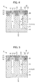
- FIG. 4 is a partial cross-sectional view schematically showing an embodiment of a semiconductor device according to the present invention.
- FIG. 5 is a partial cross-sectional view schematically showing another embodiment of a semiconductor device according to the present invention.
- the n-channel power MOSFET 2 includes: the silicon substrate 10; the first epitaxial layer 11; the second epitaxial layer 13; the third epitaxial layer 14; the fourth epitaxial layer 15; the fifth epitaxial layer 16; a source region 17; an ohmic contact region 18; and a trench insulated gate electrode 19.
- the silicon substrate 10 is a drain region.
- the first epitaxial layer 11 is an n-type epitaxial layer formed on the silicon substrate 10.
- the second epitaxial layer 13, the third epitaxial layer 14 and the fourth epitaxial layer 15 are p-type epitaxial layers.
- the second epitaxial layer 13, the third epitaxial layer 14 and the fourth epitaxial layer 15 are formed alternately on the first epitaxial layer 11 and in the trenches 12 that are formed in the first epitaxial layer 11 at predetermined intervals, to be adjacent to the first epitaxial layer 11.
- the fifth epitaxial layer 16 is a p-type epitaxial layer formed on the fourth epitaxial layer 15.
- the fifth epitaxial layer 16 functions as a channel forming layer.
- the fifth epitaxial layer 16 is a p-type epitaxial layer formed on the fourth epitaxial layer 15.
- the fifth epitaxial layer 16 functions as a channel forming layer.
- the fifth epitaxial layer 16 is formed on the fourth epitaxial layer 15, after flattening of a surface of the fourth epitaxial layer by polishing.
- the n-type source region 17 and the p-type ohmic contact region 18 are formed on the fourth epitaxial layer 15.
- the n-type source region 17 is formed by, for example, ion implantation of an n-type dopant to a p-type epitaxial layer.
- the p-type ohmic contact region 18 is formed by, for example, ion implantation of a p-type dopant.
- the trench insulated gate electrode 19 is formed to penetrate the source region 17, the fifth epitaxial layer 16, the fourth epitaxial layer 15, the third epitaxial layer 14 and a part of the second epitaxial layer 13.
- a trench 20 that penetrates the source region 17, the fifth epitaxial layer 16, the fourth epitaxial layer 15, the third epitaxial layer 14 and a part of the second epitaxial layer 13 is formed.
- an insulating film 21 is formed by a thermal oxidation method, a CVD method or the like.
- the trench insulated gate electrode 19 is composed of polycrystal silicon 22 and formed on the insulating film 21 to fill up the trench 20.
- dopant amount in the second epitaxial layer 13, the third epitaxial layer 14 and the fourth epitaxial layer 15 is constant in the whole area of the second epitaxial layer 13, the third epitaxial layer 14 and the fourth epitaxial layer 15.
- the power MOSFET 2 shown in FIG. 5 can be obtained by reversing the conductivity types of the components of the power MOSFET 2 shown in FIG. 4 .
- a semiconductor substrate and the method of producing the same according to the present invention have been described above; however, the present invention is not limited thereto.
- a conductivity type of the silicon substrate 10 and the first epitaxial layer 11 is n-type
- a conductivity type of the second epitaxial layer 13, the third epitaxial layer 14 and the fourth epitaxial layer 15 is p-type
- the present invention is not limited thereto.
- the conductivity type of the silicon substrate 10 and the first epitaxial layer 11 can be p-type
- the conductivity type of the second epitaxial layer 13, the third epitaxial layer 14 and the fourth epitaxial layer 15 can be n-type.
- a semiconductor substrate using silicon has been described in the above embodiment; however, the present invention is not limited thereto.
- a compound semiconductor such as silicon carbide (SiC), gallium arsenide (GaAs) and gallium nitride (GaN) can also be used.
- SiC silicon carbide
- GaAs gallium arsenide
- GaN gallium nitride
- the semiconductor substrate 1 shown in FIG. 1 was produced by performing the steps S1 to S5 described in the above embodiment. A temperature of an atmosphere and a dopant flow rate in formation of the second epitaxial layer 13, the third epitaxial layer 14 and a fourth epitaxial layer 15 are shown below.
- As the dopant diborane (B 2 H 6 ) gas in concentration of 100 ppm was used.
- the temperature of the atmosphere during formation of the second epitaxial layer was 970°C and the dopant gas flow rate was 220 sccm.
- the temperature of the atmosphere during formation of the third epitaxial layer was 950°C and the dopant gas flow rate was 250 sccm.
- the temperature of the atmosphere during formation of the fourth epitaxial layer was 980°C and the dopant gas flow rate was 210 sccm.
- resistivity of the semiconductor substrate 1 obtained by the steps S1 to S5 was measured and electrical characteristics thereof were evaluated using spreading resistance measurement device.
- variation in resistivity profile in a thickness direction (for example, maximum value - minimum value) was no greater than ⁇ 2%.
- the dopant gas flow rate in an atmosphere during the third epitaxial layer forming step S4 was 220 sccm. Other conditions were the same as in Example 1.
- variation in resistivity profile in a thickness direction was ⁇ 11%.
- Example 1 provided resistivity profile in a thickness direction more uniform than in Comparative Example 1.
- the dopant concentration of each of the second epitaxial layer, the third epitaxial layer and the fourth epitaxial layer does not change significantly and is substantially the same. Accordingly, Example 1 was found to provide the electrical characteristics that are suitable for production of a MOSFET having a super junction structure.
Abstract
Description
- The present invention relates to a semiconductor substrate, a semiconductor device and a method of producing a semiconductor substrate.
- Conventionally, in the field of power electronics, a power MOSFET (Metal Oxide Semiconductor Field Effect Transistor) has been used as a switching element having a high-speed switching function. As a structure of a power MOSFET, a super junction structure can be exemplified.
- In the super junction structure, an n-type layer and a p-type layer are alternately formed in a conductive layer that connects a source and a drain. In the super junction structure, a depletion layer is formed in an interface between the n-type layer and the p-type layer. Accordingly, between the source and the drain, an electric field is formed not only in a direction from the source to the drain, but also in a direction from the n-type layer to the p-type layer. As a result, the electric field between the source and the drain does not concentrate on a certain part in the conductive layer. Therefore, the super junction structure can provide high voltage resistance performance.
- As a method of producing a semiconductor substrate used for forming the super junction structure, a method of forming a trench in an epitaxial layer and forming a plurality of epitaxial layers in the trench thus formed is proposed (for example, refer to
Patent Documents 1 and 2). - [Patent Document 1] Japanese Unexamined Patent Application Publication No.
2005-294711 - [Patent Document 2] Japanese Unexamined Patent Application Publication No.
2005-317905 - However, in the method disclosed in
Patent Documents 1 and 2, temperature is different in formation of each of the epitaxial layers, and thus concentration of dopant is different in each of the epitaxial layers. This may prevent obtaining desired electrical characteristics (for example, resistivity). - The present invention is aimed at providing a semiconductor substrate, a semiconductor device and a method of producing a semiconductor substrate that are more likely to provide desired electrical characteristics.
- In a first aspect of the present invention, a method of producing a semiconductor substrate includes: a first epitaxial layer forming step of forming a first epitaxial layer by introducing a dopant gas of a first conductivity type to a semiconductor substrate of the first conductivity type; a trench forming step of forming a trench in the first epitaxial layer; and an epitaxial layer forming step of forming an epitaxial layer of a second conductivity type that is different from the first conductivity type on the first epitaxial layer and in the trench so as to fill up the trench, using a plurality of growth conditions including different growth rates, and making concentration of a dopant gas of the second conductivity type, which is incorporated into the epitaxial layer, constant in each of the plurality of growth conditions.
- According to the second aspect of the present invention, in the method of producing a semiconductor substrate as described in the first aspect, it is preferable that the plurality of growth conditions includes growth temperature of the epitaxial layer; and the growth rate is changed by changing the growth temperature of the epitaxial layer.
- According to the third aspect of the present invention, in the method of producing a semiconductor substrate as described in the first aspect, it is preferable that the plurality of growth conditions includes flow rate of the dopant gas of the second conductivity type that is introduced into the epitaxial layer and the trench; and the growth rate is changed by changing the flow rate of a material gas.
- In a fourth aspect of the present invention, a method of producing a semiconductor substrate, includes: a first epitaxial layer forming step of forming a first epitaxial layer by introducing a dopant gas of a first conductivity type to a semiconductor substrate of the first conductivity type; a trench forming step of forming a trench in the first epitaxial layer; and a second epitaxial layer forming step of forming a second epitaxial layer on the first epitaxial layer and in the trench, by introducing a dopant gas of a second conductivity type that is different from the first conductivity type at a predetermined first dopant gas flow rate, in an atmosphere of a predetermined first temperature; a third epitaxial layer forming step of forming a third epitaxial layer to fill up the trench, by introducing the dopant gas of the second conductivity type to the second epitaxial layer at a second dopant gas flow rate that is greater than the first dopant gas flow rate, in an atmosphere of a second temperature that is lower than the first temperature; a fourth epitaxial layer forming step of forming a fourth epitaxial layer by introducing the dopant gas of the second conductivity type to the second epitaxial layer and the third epitaxial layer at a third dopant gas flow rate that is lower than the second dopant gas flow rate, in an atmosphere of a third temperature that is higher than the second temperature.
- In a fifth aspect of the present invention, a method of producing a semiconductor substrate includes: a first epitaxial layer forming step of forming a first epitaxial layer by introducing a dopant gas of a first conductivity type to a semiconductor substrate of the first conductivity type; a trench forming step of forming a trench in the first epitaxial layer; and a second epitaxial layer forming step of forming a second epitaxial layer on the first epitaxial layer and in the trench, by introducing a dopant gas of a second conductivity type that is different from the first conductivity type at a predetermined first dopant gas flow rate, in an atmosphere of a predetermined first temperature; and a third epitaxial layer forming step of forming a third epitaxial layer to fill up the trench, by introducing the dopant gas of the second conductivity type to the second epitaxial layer at a second dopant gas flow rate that is greater than the first dopant gas flow rate, in an atmosphere of a second temperature that is lower than the first temperature.
- In a sixth aspect of the present invention, a method of producing a semiconductor substrate includes: a first epitaxial layer forming step of forming a first epitaxial layer by introducing a dopant gas of a first conductivity type to a semiconductor substrate of the first conductivity type; a trench forming step of forming a trench in the first epitaxial layer; a second epitaxial layer forming step of forming a second epitaxial layer on the first epitaxial layer and in the trench, by introducing a dopant gas of a second conductivity type that is different from the first conductivity type at a predetermined first dopant gas flow rate, in an atmosphere of a predetermined first temperature; and a third epitaxial layer forming step of forming a third epitaxial layer to fill up the trench, by introducing the dopant gas of the second conductivity type to the second epitaxial layer at a second dopant gas flow rate that is greater than the first dopant gas flow rate, in an atmosphere of a second temperature that is higher than the first temperature.
- According to a seventh aspect of the present invention, in the method of producing a semiconductor substrate as described in the fourth aspect, it is preferable that amount of dopant in the second epitaxial layer, the third epitaxial layer, and the fourth epitaxial layer is changed by changing the flow rate of the dopant gas of the second conductivity type.
- According to an eighth aspect of the present invention, in the method of producing a semiconductor substrate as described in the fourth aspect, it is preferable that amount of dopant in the second epitaxial layer, the third epitaxial layer, and the fourth epitaxial layer is changed by using a plurality of gas cylinders of different concentrations of the dopant gas of the second conductivity type.
- According to a ninth aspect of the present invention, in the method of producing a semiconductor substrate as described in the fourth aspect, it is preferable that at least one of the second epitaxial layer, the third epitaxial layer and the fourth epitaxial layer is formed by feeding a material gas and a halide gas in parallel in the atmosphere.
- According to a tenth aspect of the present invention, in the method of producing a semiconductor substrate as described in the fourth aspect, it is preferable that amount of dopant is substantially the same in the second epitaxial layer, the third epitaxial layer and the fourth epitaxial layer.
- According to an eleventh aspect of the present invention, in the method of producing a semiconductor substrate as described in the fourth aspect, it is preferable that a flow rate of a halide gas in the atmosphere is greater in the third epitaxial layer forming step than in the second epitaxial layer forming step and the fourth epitaxial layer forming step.
- In a twelfth aspect of the present invention, a semiconductor substrate is manufactured by the method of producing a semiconductor substrate as described in the first aspect.
- In a thirteenth aspect of the present invention, a semiconductor device uses the semiconductor substrate as described in the twelfth aspect.
- The present invention is aimed at providing a semiconductor substrate, a semiconductor device and a method of producing a semiconductor substrate that are more likely to provide desired electrical characteristics.
-
-
FIG. 1 is a partial cross-sectional view schematically showing an embodiment of a semiconductor substrate according to the present invention; -
FIG. 2 is a flow chart showing an embodiment of a method of producing the semiconductor substrate according to the present invention; -
FIG. 3A is a partial cross-sectional view sequentially showing changes in a cross section of asemiconductor substrate 1 in the method of producing a semiconductor substrate shown inFIG. 2 ; -
FIG. 3B is a partial cross-sectional view sequentially showing changes in a cross section of asemiconductor substrate 1 in the method of producing a semiconductor substrate shown inFIG. 2 ; -
FIG. 3C is a partial cross-sectional view sequentially showing changes in a cross section of asemiconductor substrate 1 in the method of producing a semiconductor substrate shown inFIG. 2 ; -
FIG. 3D is a partial cross-sectional view sequentially showing changes in a cross section of asemiconductor substrate 1 in the method of producing a semiconductor substrate shown inFIG. 2 ; -
FIG. 3E is a partial cross-sectional view sequentially showing changes in a cross section of asemiconductor substrate 1 in the method of producing a semiconductor substrate shown inFIG. 2 ; -
FIG. 4 is a partial cross-sectional view schematically showing an embodiment of a semiconductor device according to the present invention; and -
FIG. 5 is a partial cross-sectional view schematically showing another embodiment of a semiconductor device according to the present invention. - A semiconductor substrate of the present invention is described hereinafter with reference to the drawings.
FIG. 1 is a partial cross-sectional view schematically showing an embodiment of a semiconductor substrate according to the present invention. - As shown in
FIG. 1 , in thesemiconductor substrate 1 of the present embodiment, a firstepitaxial layer 11 is formed on asilicon substrate 10 and a plurality oftrenches 12 is formed in the firstepitaxial layer 11. In thetrenches 12, a secondepitaxial layer 13, the thirdepitaxial layer 14 and a fourthepitaxial layer 15 are sequentially formed. In addition, the fourthepitaxial layer 15 is formed also on the firstepitaxial layer 11. - The
silicon substrate 10 is an n+ type silicon substrate to which an n-type dopant is introduced to single crystal silicon at a high concentration. The firstepitaxial layer 11 is formed on thesilicon substrate 10. The firstepitaxial layer 11 is an n-type silicon epitaxial layer to which an n-type dopant is introduced at a lower concentration than in thesilicon substrate 10. - The plurality of
trenches 12 is formed in the firstepitaxial layer 11. A bottom face of thetrenches 12 is a main surface of thesilicon substrate 10. Thetrenches 12 are substantially in a rectangular pole shape. A side face of thetrenches 12 is an inner side face of the firstepitaxial layer 11. The secondepitaxial layer 13 is formed on a main surface of the firstepitaxial layer 11 and in thetrenches 12. The secondepitaxial layer 13 is a p-type silicon epitaxial layer to which a p-type dopant is introduced. - The third
epitaxial layer 14 is formed on the secondepitaxial layer 13. The thirdepitaxial layer 14 is a p-type silicon epitaxial layer to which a p-type dopant is introduced. Thesecond epitaxial layer 13 and thethird epitaxial layer 14 fill up almost an entirety of thetrenches 12 except for a part thereof. - The
fourth epitaxial layer 15 is formed on a main surface of thesecond epitaxial layer 13 and a main surface of thethird epitaxial layer 14 that are formed on the main surface of thefirst epitaxial layer 11, as well as in the part of thetrenches 12 that has not been filled. Thefourth epitaxial layer 15 is a p-type silicon epitaxial layer to which a p-type dopant is introduced. - Here, the
first epitaxial layer 11 is composed of an n-type epitaxial layer to which a dopant such as P (phosphorus), As (arsenic), Sb (antimony) and the like is introduced. In addition, thesecond epitaxial layer 13, thethird epitaxial layer 14, and thefourth epitaxial layer 15 are composed of a p-type epitaxial layer to which a dopant such as B (boron), Ga (gallium) and In (indium) is introduced. - A conductivity type of the
second epitaxial layer 13, thethird epitaxial layer 14 and thefourth epitaxial layer 15 is different from that of thefirst epitaxial layer 11. A conductivity type that is different is p-type for n-type, or n-type for p-type. Therefore, for example, if a conductivity type of thefirst epitaxial layer 11 is n-type, a conductivity type of thesecond epitaxial layer 13, thethird epitaxial layer 14 and thefourth epitaxial layer 15 is p-type. - As desribed above, the
semiconductor substrate 1 has a super junction structure in which thefirst epitaxial layer 11 that is n-type, thesecond epitaxial layer 13, thethird epitaxial layer 14, and thefourth epitaxial layer 15 that are p-type are formed alternately on thesilicon substrate 10. - Here, provided that: a width of the
first epitaxial layer 11 is H1 (µm); a width of thesecond epitaxial layer 13, thethird epitaxial layer 14, and thefourth epitaxial layer 15 is H2 (µm); carrier concentration of thefirst epitaxial layer 11 is C1 (cm-3); and carrier concentration of thesecond epitaxial layer 13, thethird epitaxial layer 14, and thefourth epitaxial layer 15 is C2 (cm-3), at least one of the width H1 of thefirst epitaxial layer 11 and the width H2 of thesecond epitaxial layer 13, thethird epitaxial layer 14, and thefourth epitaxial layer 15 fulfils an equation C1 × H1 = C2 × H2. Therefore, amount of dopant included in thefirst epitaxial layer 11 and amount of dopant included in thesecond epitaxial layer 13, thethird epitaxial layer 14 and thefourth epitaxial layer 15 are substantially the same. As a result, a p-n junction between: thefirst epitaxial layer 11 that is n-type; and thesecond epitaxial layer 13, thethird epitaxial layer 14, and thefourth epitaxial layer 15 that are p-type, provides a depletion layer to fully deplete a drift region, thereby maintaining high voltage resistance performance. - A method of producing a semiconductor substrate according to the present embodiment is hereinafter described with reference to
FIGS. 2 and3 .FIG. 2 is a flow chart showing an embodiment of a method of producing the semiconductor substrate according to the present invention.FIGS. 3A to 3E are partial cross-sectional views sequentially showing changes in thesemiconductor substrate 1 in the method of producing a semiconductor substrate shown inFIG. 2 . - As shown in
FIG. 2 , the method of producing a semiconductor substrate according to the present embodiment includes: a first epitaxial layer forming step S1; a trench forming step S2; a second epitaxial layer forming step S3; a third epitaxial layer forming step S4; and a fourth epitaxial layer forming step S5. Each step (S1 to S5) is described hereinafter, with reference toFIG. 3 as necessary. - As shown in
FIG. 3A , an n-type dopant gas is supplied while supplying a material gas to thesilicon substrate 10 of n+ type, thereby forming thefirst epitaxial layer 11 in an atmosphere containing the material gas and the dopant gas. - Here, as the material gas (silicon source gas), SiH4 (monosilane), Si2H6 (disilane), SiH2Cl2 (dichlorosilane), SiHCl3 (trichlorosilane), SiCl4 (silicon tetrachloride) and the like can be exemplified.
- As the dopant gas for formation of an n-type epitaxial layer, phosphine (PH3) that contain phosphorus (P) and arsine (AsH3) that contain arsenic (As), which are n-type dopants, can be exemplified. On the other hand, as the dopant gas for formation of a p-type epitaxial layer, diborane (B2H6) and boron trichloride (BCl3) that contain boron (B), which are p-type dopants, can be exemplified. As for the material gas and the dopant gas, the abovementioned gases can be used similarly in the second epitaxial layer forming step S3, the third epitaxial layer forming step S4 and the fourth epitaxial layer forming step S5 that are described later.
- Although a method for forming the
first epitaxial layer 11, thesecond epitaxial layer 13, thethird epitaxial layer 14 and thefourth epitaxial layer 15 is not particularly limited, chemical vapor deposition (CVD), physical vapor deposition (PVD), molecular beam epitaxy (MBE) and the like are preferably used. - As shown in
FIG. 3B , a resist pattern is formed by photolithography at a predetermined position on thefirst epitaxial layer 11 formed in the first epitaxial layer forming step S1. And then, a region in which the resist pattern is not formed on thefirst epitaxial layer 11 is etched by, for example, reactive ion etching, thereby forming thetrenches 12. Thereafter, thetrenches 12 shown inFIG. 3B are obtained by removing the resist pattern. - As shown in
FIG. 3C , after the trench forming step S2, a p-type dopant gas is introduced to thefirst epitaxial layer 11 and thetrenches 12, while supplying the material gas and the halide gas thereto, thereby forming thesecond epitaxial layer 13 in an atmosphere containing the material gas, the halide gas, and the dopant gas. A temperature of the atmosphere containing the material gas, the halide gas, and the dopant gas is preferably 950 to 1000°C (predetermined first temperature), and a flow rate of the dopant gas (predetermined first dopant gas flow rate) is preferably 100 to 300 sccm (Standard Cubic Centimeter per Minute). In addition, an amount of dopant in the second epitaxial layer 13 (first dopant amount) is preferably 1×10¹⁵ to 1×10¹⁷ (cm-3). - In the present embodiment, the dopant amount is a value defined, before incorporation of a dopant gas by an epitaxial layer, by a flow rate and concentration of the dopant gas; and, after incorporation of the dopant gas by the epitaxial layer, defined by a density of dopant atoms in a crystal lattice of the epitaxial layer.
- As the halide gas, HCl (hydrogen chloride), Cl2 (chlorine), F2 (fluorine), CLF3 (chlorine trifluoride), HF (hydrogen fluoride), HBr (hydrogen bromide) and the like can be exemplified. As for the halide gas, the abovementioned gases can be used similarly in the third epitaxial layer forming step S4 and the fourth epitaxial layer forming step S5 that are described later.
- In a case of supplying the material gas and the halide gas, the halide gas functions as an etching gas inside the
trenches 12. Since an etching rate of the halide gas is slower in a bottom part of thetrenches 12 than in an opening part of thetrenches 12, a formation rate of an epitaxial layer is faster in the bottom part than in the opening part of thetrenches 12. Generation of a void in thesecond epitaxial layer 13 formed in thetrenches 12 can thus be prevented. - As shown in
FIG. 3D , after the second epitaxial layer forming step S3, a p-type dopant gas is introduced to thesecond epitaxial layer 13, while supplying the material gas and the halide gas thereto, thereby forming thethird epitaxial layer 14 to fill up thetrenches 12, in an atmosphere containing the material gas, the halide gas, and the dopant gas. Thethird epitaxial layer 14 is formed also in a region on thesecond epitaxial layer 13, outside of thetrenches 12. A temperature of the atmosphere containing the material gas, the halide gas, and the dopant gas is 900 to 950°C (second temperature), which is lower than that in the second epitaxial layer forming step S3. In addition, a flow rate of the p-type dopant gas (second dopant gas flow rate), is 110 to 360 sccm, which is higher than that in the second epitaxial layer forming step S3. In addition, an amount of dopant in the third epitaxial layer 14 (second dopant amount) is preferably 1×10¹⁵ to 1×10¹⁷ (cm-3). - A difference between the temperature of the atmosphere in the second epitaxial layer forming step S3 and the temperature of the atmosphere in the third epitaxial layer forming step S4 is preferably at least 10°C, and more preferably at least 50°C. In addition, a difference between the flow rate of the p-type dopant gas in the second epitaxial layer forming step S3 and the flow rate of the p-type dopant gas in the third epitaxial layer forming step S4 is preferably at least 5 sccm, and more preferably at least 30 sccm.
- By going through the third epitaxial layer forming step S4, the
second epitaxial layer 13 and thethird epitaxial layer 14. fill up almost an entirety of thetrenches 12 except for a part thereof. A temperature of the atmosphere in the third epitaxial layer forming step S4 is lower than that in the second epitaxial layer forming step S3. Generation of a void and crystal defect in thethird epitaxial layer 14 can thus be prevented. - As shown in
FIG. 3E , after the third epitaxial layer forming step S4, a p-type dopant gas is introduced to thesecond epitaxial layer 13 and thethird epitaxial layer 14, while supplying the material gas and the halide gas thereto, thereby forming thefourth epitaxial layer 15 in an atmosphere containing the material gas, the halide gas, and the dopant gas. A temperature of the atmosphere containing the material gas, the halide gas, and the dopant gas is 950 to 1000°C (third temperature), which is higher than that in the third epitaxial layer forming step S4. In addition, a flow rate of the p-type dopant gas (third dopant gas flow rate), is 100 to 300 sccm, which is lower than that in the third epitaxial layer forming step S4. In addition, an amount of dopant in the fourth epitaxial layer 15 (third dopant amount) is preferably 1×10¹⁵ to 1×10¹⁷ (cm-3). - A difference between the temperature of the atmosphere in the fourth epitaxial layer forming step S5 and the temperature of the atmosphere in the third epitaxial layer forming step S4 is preferably at least 10°C, and more preferably at least 50°C. In addition, a difference between the flow rate of the p-type dopant gas in the fourth epitaxial layer forming step S5 and the flow rate of the p-type dopant gas in the third epitaxial layer forming step S4 is preferably at least 5 sccm, and more preferably at least 30 sccm.
- In the abovementioned embodiment, a conductivity type of the
silicon substrate 10 and thefirst epitaxial layer 11 is n-type, and a conductivity type of thesecond epitaxial layer 13, thethird epitaxial layer 14 and thefourth epitaxial layer 15 is p-type; however, the present invention is not limited thereto. For example, the conductivity type of thesilicon substrate 10 and thefirst epitaxial layer 11 can be p-type, and the conductivity type of thesecond epitaxial layer 13, thethird epitaxial layer 14 and thefourth epitaxial layer 15 can be n-type. - In this case, a flow rate of the n-type dopant gas in the third epitaxial layer forming step S4 is lower than that in the second epitaxial layer forming step S3. In addition, a flow rate of the n-type dopant gas in the fourth epitaxial layer forming step S5 is lower than that in the third epitaxial layer forming step S4.
- As described above, in the method of producing a semiconductor substrate according to the present embodiment, the
second epitaxial layer 13, thethird epitaxial layer 14 and thefourth epitaxial layer 15 are formed on thefirst epitaxial layer 11 and thetrenches 12 to fill up thetrenches 12, using a plurality of growth conditions including different growth rates. In this case, in the method of producing a semiconductor substrate according to the present embodiment, in each of the plurality of growth conditions, concentration of the p-type dopant incorporated into thesecond epitaxial layer 13, thethird epitaxial layer 14 and thefourth epitaxial layer 15 is constant. - Here, the plurality of growth conditions includes growth temperature of the
second epitaxial layer 13, thethird epitaxial layer 14 and thefourth epitaxial layer 15. The abovementioned growth rate is changed by changing the growth temperature of thesecond epitaxial layer 13, thethird epitaxial layer 14 and thefourth epitaxial layer 15. - In addition, the plurality of growth conditions can include a flow rate of the p-type dopant gas incorporated into the
trenches 12, thesecond epitaxial layer 13, thethird epitaxial layer 14 and thefourth epitaxial layer 15. In this case, the growth rate is changed by changing the flow rate of the material gas (silicon source gas). - More specifically, a temperature of the atmosphere in the second epitaxial layer forming step S3 and the fourth epitaxial layer forming step S5 (approximately 950 to 1000°C) is higher than that in the third epitaxial layer forming step S4 (approximately 900 to 950°C). As a result, in the second epitaxial layer forming step S3 and the fourth epitaxial layer forming step S5, a formation rate of the
second epitaxial layer 13 and thefourth epitaxial layer 15 can be increased and throughput can be improved. - In addition, since a temperature of the atmosphere in the second epitaxial layer forming step S3 and the fourth epitaxial layer forming step S5 (approximately 950 to 1000°C) is higher than that in the third epitaxial layer forming step S4 (approximately 900 to 950°C), dopant concentration in the
third epitaxial layer 14 tends to be lower than that of thesecond epitaxial layer 13 and thefourth epitaxial layer 15. Accordingly, in order to suppress change in the dopant concentration, a flow rate of the dopant gas in the third epitaxial layer forming step S4 is set to be lower than that in the second epitaxial layer forming step S3 and the fourth epitaxial layer forming step S5. - At least one of the
second epitaxial layer 13, thethird epitaxial layer 14 and thefourth epitaxial layer 15 is preferably formed by feeding a material gas and a halide gas in parallel in the atmosphere. More specifically, for example thesecond epitaxial layer 13 and thethird epitaxial layer 14 are formed by feeding a material gas and a halide gas in parallel in the atmosphere of the second epitaxial layer forming step S3 and the third epitaxial layer forming step S4. - In addition, the flow rate of the halide gas in the atmosphere is preferably greater in the third epitaxial layer forming step S4 than in the second epitaxial layer forming step S3 and the fourth epitaxial layer forming step S5.
- In addition, the dopant concentration or the dopant amount of the
second epitaxial layer 13, thethird epitaxial layer 14 and thefourth epitaxial layer 15 is preferably substantially the same. The dopant concentration being substantially the same means that a difference in the dopant amount is no greater than ±5%. - According to the method of manufacturing a semiconductor substrate according to the present embodiment, the following effect is provided for example. The method of producing a semiconductor substrate according to the present embodiment is provided with: the first epitaxial layer forming step S1 of forming the
first epitaxial layer 11; the trench forming step S2 of forming the trenches in the first epitaxial layer; the second epitaxial layer forming step S3 of forming the second epitaxial layer on thefirst epitaxial layer 11 and inside thetrenches 12; the third epitaxial layer forming step S4 of forming thethird epitaxial layer 14 on thesecond epitaxial layer 13; and the fourth epitaxial layer forming step S5 of forming the fourth epitaxial layer on the second epitaxial layer and the third epitaxial layer. - In addition, a temperature of the atmosphere in the second epitaxial layer forming step S3 and the fourth epitaxial layer forming step S5 is higher than that in the third epitaxial layer forming step S4, and a flow rate of the dopant gas in the third epitaxial layer forming step S4 is higher than in the second epitaxial layer forming step S3 and the fourth epitaxial layer forming step S5.
- As a result, since the dopant concentration of the
second epitaxial layer 13, thethird epitaxial layer 14, and thefourth epitaxial layer 15 can be made substantially the same, in resistivity measurement of thesemiconductor substrate 1, for example, resistivity of thesecond epitaxial layer 13, thethird epitaxial layer 14; and thefourth epitaxial layer 15 is substantially the same. In other words, the method of producing a semiconductor substrate of the present embodiment can provide desired electrical characteristics. Therefore, a power MOSFET that is manufactured using thesemiconductor substrate 1 including thesecond epitaxial layer 13, thethird epitaxial layer 14, and thefourth epitaxial layer 15 of the present embodiment (seeFIG. 4 or 5 ) can provide desired electrical characteristics such as high voltage resistance performance and on resistance. - The method of producing a semiconductor substrate can provide the same effect even if a flow rate of at least one of the material gas and the halide gas is changed.
- In the abovementioned embodiment, the growth temperature is changed in three levels in the second epitaxial layer forming step S3, the third epitaxial layer forming step S4 and the fourth epitaxial layer forming step S5; however, the present invention is not limited thereto. In the method of producing a semiconductor substrate of the present invention, the growth temperature of the epitaxial layer inside the
trenches 12 can be changed in two levels, for example. In a case of changing the growth temperature in two levels, for example, the growth temperature of the epitaxial layer can be changed from approximately 950 to 1000°C to approximately 900 to 950°C, or from approximately 900 to 950°C to approximately 950 to 1000°C. - In other words, the method of producing a semiconductor substrate according to the present invention can include: the first epitaxial layer forming step S1 the trench forming step S2; the second epitaxial layer forming step S3; and the third epitaxial layer forming step S4.
- In this case, in the second epitaxial layer forming step S3, the
second epitaxial layer 13 of p-type is formed by introducing a p-type dopant gas to thefirst epitaxial layer 11 and thetrenches 12 of n-type, at the first dopant gas flow rate, in an atmosphere of approximately 950 to 1000°C. - In addition, in the third epitaxial layer forming step S4, the
third epitaxial layer 14 of p-type is formed to fill up thetrenches 12, by introducing a p-type dopant gas to thesecond epitaxial layer 13, at the second dopant gas flow rate that is higher than the first dopant gas flow rate, in an atmosphere of approximately 900 to 950°C. - Alternatively, in a case in which the
first epitaxial layer 11 is p-type and thesecond epitaxial layer 13 and thethird epitaxial layer 14 are n-type, in the second epitaxial layer forming step S3, thesecond epitaxial layer 13 is formed by introducing an n-type dopant gas to thefirst epitaxial layer 11 and thetrenches 12, at the first dopant gas flow rate, in an atmosphere of approximately 950 to 1000°C. In addition, in the third epitaxial layer forming step S4, thethird epitaxial layer 14 of n-type is formed to fill up thetrenches 12, by introducing an n-type dopant gas at the second dopant gas flow rate that is lower than the first dopant gas flow rate, in an atmosphere of approximately 900 to 950°C. - As described above, in the second epitaxial layer forming step S3, the
second epitaxial layer 13 is formed in an atmosphere of approximately 950 to 1000°C. In the third epitaxial layer forming step S4, thethird epitaxial layer 14 is formed in an atmosphere of approximately 900 to 950°C, a growth temperature lower than that of thesecond epitaxial layer 13. In this case, thefourth epitaxial layer 15 is not formed and thesecond epitaxial layer 13 and thethird epitaxial layer 14 are formed to fill up thetrenches 12. - Furthermore, in the second epitaxial layer forming step 33, the
second epitaxial layer 13 can be formed by introducing a p-type dopant gas to thefirst epitaxial layer 11 and thetrenches 12, at the first dopant gas flow rate, in an atmosphere of approximately 900 to 950°C. - In addition, in the third epitaxial layer forming step S4, the
third epitaxial layer 14 can be formed to fill up thetrenches 12, by introducing a p-type dopant gas to thesecond epitaxial layer 13, at the second dopant gas flow rate that is higher than the first dopant gas flow rate, in an atmosphere of approximately 950 to 1000°C. In this case, thefourth epitaxial layer 15 is not formed and thesecond epitaxial layer 13 and thethird epitaxial layer 14 are formed to fill up thetrenches 12. - In a case in which the
first epitaxial layer 11 is p-type and thesecond epitaxial layer 13 and thethird epitaxial layer 14 are n-type, in the second epitaxial layer forming step S3, thesecond epitaxial layer 13 can be formed by introducing an n-type dopant gas to thefirst epitaxial layer 11 and thetrenches 12, at the first dopant gas flow rate, in an atmosphere of approximately 900 to 950°C. In addition, in the third epitaxial layer forming step S4, thethird epitaxial layer 14 can be formed to fill up thetrenches 12, by introducing an n-type dopant gas at the second dopant gas flow rate that is lower than the first dopant gas flow rate, in an atmosphere of approximately 950 to 1000°C. In this case, thefourth epitaxial layer 15 is not formed and thesecond epitaxial layer 13 and thethird epitaxial layer 14 are formed to fill up thetrenches 12. - Here, the first dopant amount of the
second epitaxial layer 13, the second dopant amount of thethird epitaxial layer 14, and the third dopant amount of thefourth epitaxial layer 15 are changed by changing the flow rate of the dopant gas of p-type or n-type. In addition, the first dopant amount, the second dopant amount and the third dopant amount are changed by using a plurality of cylinders of different concentrations of the dopant gas of p-type and n-type. - As described above, in the method of producing a semiconductor substrate of the present invention, the growth temperature can be changed in four levels, not in two or three levels, and the epitaxial layer can be formed inside the
trenches 12 while consecutively changing the growth temperature. In addition, although only the growth temperature is changed in the method of producing a semiconductor substrate according to the abovementioned embodiment; however, the present invention is not limited thereto. For example, in the method of producing a semiconductor substrate, the flow rate of at least one of the material gas and the halide gas can be changed. - Next, a structure of a power MOSFET 2 as a semiconductor device produced using the
semiconductor substrate 1 according to the present embodiment is hereinafter described with reference toFIGS. 4 and 5. FIG. 4 is a partial cross-sectional view schematically showing an embodiment of a semiconductor device according to the present invention.FIG. 5 is a partial cross-sectional view schematically showing another embodiment of a semiconductor device according to the present invention. - As shown in
FIG. 4 , the n-channel power MOSFET 2 includes: thesilicon substrate 10; thefirst epitaxial layer 11; thesecond epitaxial layer 13; thethird epitaxial layer 14; thefourth epitaxial layer 15; thefifth epitaxial layer 16; asource region 17; anohmic contact region 18; and a trench insulatedgate electrode 19. - The
silicon substrate 10 is a drain region. As described above, thefirst epitaxial layer 11 is an n-type epitaxial layer formed on thesilicon substrate 10. - The
second epitaxial layer 13, thethird epitaxial layer 14 and thefourth epitaxial layer 15 are p-type epitaxial layers. Thesecond epitaxial layer 13, thethird epitaxial layer 14 and thefourth epitaxial layer 15 are formed alternately on thefirst epitaxial layer 11 and in thetrenches 12 that are formed in thefirst epitaxial layer 11 at predetermined intervals, to be adjacent to thefirst epitaxial layer 11. - The
fifth epitaxial layer 16 is a p-type epitaxial layer formed on thefourth epitaxial layer 15. Thefifth epitaxial layer 16 functions as a channel forming layer. - The
fifth epitaxial layer 16 is a p-type epitaxial layer formed on thefourth epitaxial layer 15. Thefifth epitaxial layer 16 functions as a channel forming layer. For example, thefifth epitaxial layer 16 is formed on thefourth epitaxial layer 15, after flattening of a surface of the fourth epitaxial layer by polishing. - The n-
type source region 17 and the p-typeohmic contact region 18 are formed on thefourth epitaxial layer 15. The n-type source region 17 is formed by, for example, ion implantation of an n-type dopant to a p-type epitaxial layer. The p-typeohmic contact region 18 is formed by, for example, ion implantation of a p-type dopant. - The trench insulated
gate electrode 19 is formed to penetrate thesource region 17, thefifth epitaxial layer 16, thefourth epitaxial layer 15, thethird epitaxial layer 14 and a part of thesecond epitaxial layer 13. For example, in a step of forming the trench insulatedgate electrode 19, atrench 20 that penetrates thesource region 17, thefifth epitaxial layer 16, thefourth epitaxial layer 15, thethird epitaxial layer 14 and a part of thesecond epitaxial layer 13 is formed. On a bottom face and lateral face of thetrench 20, an insulatingfilm 21 is formed by a thermal oxidation method, a CVD method or the like. The trench insulatedgate electrode 19 is composed ofpolycrystal silicon 22 and formed on the insulatingfilm 21 to fill up thetrench 20. - In the power MOSFET 2 thus obtained, dopant amount in the
second epitaxial layer 13, thethird epitaxial layer 14 and thefourth epitaxial layer 15 is constant in the whole area of thesecond epitaxial layer 13, thethird epitaxial layer 14 and thefourth epitaxial layer 15. In addition, the power MOSFET 2 shown inFIG. 5 can be obtained by reversing the conductivity types of the components of the power MOSFET 2 shown inFIG. 4 . - A semiconductor substrate and the method of producing the same according to the present invention have been described above; however, the present invention is not limited thereto. For example, a conductivity type of the
silicon substrate 10 and thefirst epitaxial layer 11 is n-type, and a conductivity type of thesecond epitaxial layer 13, thethird epitaxial layer 14 and thefourth epitaxial layer 15 is p-type; however, the present invention is not limited thereto. For example, the conductivity type of thesilicon substrate 10 and thefirst epitaxial layer 11 can be p-type, and the conductivity type of thesecond epitaxial layer 13, thethird epitaxial layer 14 and thefourth epitaxial layer 15 can be n-type. - In addition, a semiconductor substrate using silicon has been described in the above embodiment; however, the present invention is not limited thereto. For example, a compound semiconductor such as silicon carbide (SiC), gallium arsenide (GaAs) and gallium nitride (GaN) can also be used. (
 ) EXAMPLES
- Next, the present invention is described further in detail using Examples. Examples are not intended to limit the scope of the present invention.
- The
semiconductor substrate 1 shown inFIG. 1 was produced by performing the steps S1 to S5 described in the above embodiment. A temperature of an atmosphere and a dopant flow rate in formation of thesecond epitaxial layer 13, thethird epitaxial layer 14 and afourth epitaxial layer 15 are shown below. As the dopant, diborane (B2H6) gas in concentration of 100 ppm was used. - The temperature of the atmosphere during formation of the second epitaxial layer was 970°C and the dopant gas flow rate was 220 sccm. The temperature of the atmosphere during formation of the third epitaxial layer was 950°C and the dopant gas flow rate was 250 sccm. The temperature of the atmosphere during formation of the fourth epitaxial layer was 980°C and the dopant gas flow rate was 210 sccm.
- Thereafter, resistivity of the
semiconductor substrate 1 obtained by the steps S1 to S5 was measured and electrical characteristics thereof were evaluated using spreading resistance measurement device. In Example 1, variation in resistivity profile in a thickness direction (for example, maximum value - minimum value) was no greater than ±2%. - Unlike Example 1, the dopant gas flow rate in an atmosphere during the third epitaxial layer forming step S4 was 220 sccm. Other conditions were the same as in Example 1. In Comparative Example 1, variation in resistivity profile in a thickness direction was ±11%.
- Evaluation results of Example 1 and Comparative Example 1 show the following, for example. Example 1 provided resistivity profile in a thickness direction more uniform than in Comparative Example 1. In other words, the dopant concentration of each of the second epitaxial layer, the third epitaxial layer and the fourth epitaxial layer does not change significantly and is substantially the same. Accordingly, Example 1 was found to provide the electrical characteristics that are suitable for production of a MOSFET having a super junction structure.
-
- 1 Semiconductor substrate
- 10 Silicon substrate
- 11 First epitaxial layer
- 12 Trench
- 13 Second epitaxial layer (epitaxial layer)
- 14 Third epitaxial layer (epitaxial layer)
- 15 Fourth epitaxial layer (epitaxial layer)
- S1 First epitaxial layer forming step
- S2 Trench forming step
- S3 Second epitaxial layer forming step (epitaxial layer forming step)
- S4 Third epitaxial layer forming step (epitaxial layer forming step)
- S5 Fourth epitaxial layer forming step (epitaxial layer forming step)
Claims (13)
- A method of producing a semiconductor substrate, the method comprising:a first epitaxial layer forming step of forming a first epitaxial layer by introducing a dopant gas of a first conductivity type to a semiconductor substrate of the first conductivity type;a trench forming step of forming a trench in the first epitaxial layer; andan epitaxial layer forming step of forming an epitaxial layer of a second conductivity type that is different from the first conductivity type on the first epitaxial layer and in the trench so as to fill up the trench, using a plurality of growth conditions including different growth rates, and making concentration of a dopant gas of the second conductivity type, which is incorporated into the epitaxial layer, constant in each of the plurality of growth conditions.
- The method of producing a semiconductor substrate according to claim 1, wherein: the plurality of growth conditions includes growth temperature of the epitaxial layer; and the growth rate is changed by changing the growth temperature of the epitaxial layer.
- The method of producing a semiconductor substrate according to claim 1, wherein: the plurality of growth conditions includes flow rate of the dopant gas of the second conductivity type that is introduced into the epitaxial layer and the trench; and the growth rate is changed by changing the flow rate of a material gas.
- A method of producing a semiconductor substrate, the method comprising:a first epitaxial layer forming step of forming a first epitaxial layer by introducing a dopant gas of a first conductivity type to a semiconductor substrate of the first conductivity type;a trench forming step of forming a trench in the first epitaxial layer; anda second epitaxial layer forming step of forming a second epitaxial layer on the first epitaxial layer and in the trench, by introducing a dopant gas of a second conductivity type that is different from the first conductivity type at a predetermined first dopant gas flow rate, in an atmosphere of a predetermined first temperature;a third epitaxial layer forming step of forming a third epitaxial layer to fill up the trench, by introducing the dopant gas of the second conductivity type to the second epitaxial layer at a second dopant gas flow rate that is greater than the first dopant gas flow rate, in an atmosphere of a second temperature that is lower than the first temperature;a fourth epitaxial layer forming step of forming a fourth epitaxial layer by introducing the dopant gas of the second conductivity type to the second epitaxial layer and the third epitaxial layer at a third dopant gas flow rate that is lower than the second dopant gas flow rate, in an atmosphere of a third temperature that is higher than the second temperature.
- A method of producing a semiconductor substrate, the method comprising:a first epitaxial layer forming step of forming a first epitaxial layer by introducing a dopant gas of a first conductivity type to a semiconductor substrate of the first conductivity type;a trench forming step of forming a trench in the first epitaxial layer;a second epitaxial layer forming step of forming a second epitaxial layer on the first epitaxial layer and in the trench, by introducing a dopant gas of a second conductivity type that is different from the first conductivity type at a predetermined first dopant gas flow rate, in an atmosphere of a predetermined first temperature; anda third epitaxial layer forming step of forming a third epitaxial layer to fill up the trench, by introducing the dopant gas of the second conductivity type to the second epitaxial layer at a second dopant gas flow rate that is greater than the first dopant gas flow rate, in an atmosphere of a second temperature that is lower than the first temperature.
- A method of producing a semiconductor substrate, the method comprising:a first epitaxial layer forming step of forming a first epitaxial layer by introducing a dopant gas of a first conductivity type to a semiconductor substrate of the first conductivity type;a trench forming step of forming a trench in the first epitaxial layer;a second epitaxial layer forming step of forming a second epitaxial layer on the first epitaxial layer and in the trench, by introducing a dopant gas of a second conductivity type that is different from the first conductivity type at a predetermined first dopant gas flow rate, in an atmosphere of a predetermined first temperature; anda third epitaxial layer forming step of forming a third epitaxial layer to fill up the trench, by introducing the dopant gas of the second conductivity type to the second epitaxial layer at a second dopant gas flow rate that is greater than the first dopant gas flow rate, in an atmosphere of a second temperature that is higher than the first temperature.
- The method of producing a semiconductor substrate according to claim 4, wherein amount of dopant in the second epitaxial layer, the third epitaxial layer, and the fourth epitaxial layer is changed by changing the flow rate of the dopant gas of the second conductivity type.
- The method of producing a semiconductor substrate according to claim 4, wherein amount of dopant in the second epitaxial layer, the third epitaxial layer, and the fourth epitaxial layer is changed by using a plurality of gas cylinders of different concentrations of the dopant gas of the second conductivity type.
- The method of producing a semiconductor substrate according to claim 4, wherein at least one of the second epitaxial layer, the third epitaxial layer and the fourth epitaxial layer is formed by feeding a material gas and a halide gas in parallel in the atmosphere.
- The method of producing a semiconductor substrate according to claim 4, wherein amount of dopant is substantially the same in the second epitaxial layer, the third epitaxial layer and the fourth epitaxial layer.
- The method of producing a semiconductor substrate according to claim 4, wherein a flow rate of a halide gas in the atmosphere is greater in the third epitaxial layer forming step than in the second epitaxial layer forming step and the fourth epitaxial layer forming step.
- A semiconductor substrate, wherein the semiconductor substrate is manufactured by the method of producing a semiconductor substrate according to claim 1.
- A semiconductor device, wherein the semiconductor substrate according to claim 12 is used.
Applications Claiming Priority (2)
| Application Number | Priority Date | Filing Date | Title |
|---|---|---|---|
| JP2009076472 | 2009-03-26 | ||
| PCT/JP2010/002152 WO2010109892A1 (en) | 2009-03-26 | 2010-03-25 | Semiconductor substrate, semiconductor device, and method of producing semiconductor substrate |
Publications (3)
| Publication Number | Publication Date |
|---|---|
| EP2413348A1 true EP2413348A1 (en) | 2012-02-01 |
| EP2413348A4 EP2413348A4 (en) | 2014-02-26 |
| EP2413348B1 EP2413348B1 (en) | 2020-11-18 |
Family
ID=42780588
Family Applications (1)
| Application Number | Title | Priority Date | Filing Date |
|---|---|---|---|
| EP10755694.6A Active EP2413348B1 (en) | 2009-03-26 | 2010-03-25 | Semiconductor substrate, semiconductor device, and method of producing semiconductor substrate |
Country Status (5)
| Country | Link |
|---|---|
| US (1) | US8501598B2 (en) |
| EP (1) | EP2413348B1 (en) |
| JP (1) | JP5636203B2 (en) |
| CN (1) | CN102362336B (en) |
| WO (1) | WO2010109892A1 (en) |
Families Citing this family (10)
| Publication number | Priority date | Publication date | Assignee | Title |
|---|---|---|---|---|
| JP5706674B2 (en) * | 2010-11-24 | 2015-04-22 | セイコーインスツル株式会社 | Constant current circuit and reference voltage circuit |
| JP5812029B2 (en) | 2012-06-13 | 2015-11-11 | 株式会社デンソー | Silicon carbide semiconductor device and manufacturing method thereof |
| JP2013258327A (en) * | 2012-06-13 | 2013-12-26 | Toshiba Corp | Semiconductor device and method of manufacturing the same |
| JP2015162492A (en) * | 2014-02-26 | 2015-09-07 | 豊田合成株式会社 | Semiconductor device manufacturing method |
| JP6150075B2 (en) * | 2014-05-01 | 2017-06-21 | 信越半導体株式会社 | Epitaxial wafer manufacturing method |
| WO2017105414A1 (en) | 2015-12-15 | 2017-06-22 | General Electric Company | Edge termination designs for silicon carbide super-junction power devices |
| CN106876463A (en) * | 2016-12-28 | 2017-06-20 | 全球能源互联网研究院 | A kind of superjunction silicon carbide device and preparation method thereof |
| JP6857351B2 (en) * | 2017-02-28 | 2021-04-14 | 国立研究開発法人産業技術総合研究所 | Silicon Carbide Semiconductor Device and Method for Manufacturing Silicon Carbide Semiconductor Device |
| JP7089329B2 (en) * | 2018-11-13 | 2022-06-22 | 株式会社豊田中央研究所 | Semiconductor devices and their manufacturing methods |
| JP7077252B2 (en) * | 2019-02-27 | 2022-05-30 | 株式会社東芝 | Manufacturing method of semiconductor device |
Family Cites Families (9)
| Publication number | Priority date | Publication date | Assignee | Title |
|---|---|---|---|---|
| CN100565801C (en) * | 2004-03-31 | 2009-12-02 | 株式会社电装 | The manufacture method of semiconductor device |
| JP4773716B2 (en) | 2004-03-31 | 2011-09-14 | 株式会社デンソー | Manufacturing method of semiconductor substrate |
| JP3961503B2 (en) * | 2004-04-05 | 2007-08-22 | 株式会社Sumco | Manufacturing method of semiconductor wafer |
| JP4939760B2 (en) * | 2005-03-01 | 2012-05-30 | 株式会社東芝 | Semiconductor device |
| JP5015440B2 (en) * | 2005-09-29 | 2012-08-29 | 株式会社デンソー | Manufacturing method of semiconductor substrate |
| DE102006045912B4 (en) | 2005-09-29 | 2011-07-21 | Sumco Corp. | Method of fabricating a semiconductor device and epitaxial growth device |
| JP5150048B2 (en) * | 2005-09-29 | 2013-02-20 | 株式会社デンソー | Manufacturing method of semiconductor substrate |
| US8304311B2 (en) * | 2006-04-11 | 2012-11-06 | Stmicroelectronics S.R.L. | Process for manufacturing a semiconductor power device comprising charge-balance column structures and respective device |
| JP5217257B2 (en) * | 2007-06-06 | 2013-06-19 | 株式会社デンソー | Semiconductor device and manufacturing method thereof |
-
2010
- 2010-03-25 EP EP10755694.6A patent/EP2413348B1/en active Active
- 2010-03-25 JP JP2010071059A patent/JP5636203B2/en active Active
- 2010-03-25 US US13/258,268 patent/US8501598B2/en active Active
- 2010-03-25 WO PCT/JP2010/002152 patent/WO2010109892A1/en not_active Ceased
- 2010-03-25 CN CN201080013387.4A patent/CN102362336B/en active Active
Also Published As
| Publication number | Publication date |
|---|---|
| WO2010109892A1 (en) | 2010-09-30 |
| US8501598B2 (en) | 2013-08-06 |
| US20120032312A1 (en) | 2012-02-09 |
| CN102362336A (en) | 2012-02-22 |
| JP5636203B2 (en) | 2014-12-03 |
| CN102362336B (en) | 2014-03-12 |
| EP2413348B1 (en) | 2020-11-18 |
| JP2010251737A (en) | 2010-11-04 |
| EP2413348A4 (en) | 2014-02-26 |
Similar Documents
| Publication | Publication Date | Title |
|---|---|---|
| US8501598B2 (en) | Semiconductor substrate, semiconductor device, and method of producing semiconductor substrate | |
| US9673296B2 (en) | Semiconductor structure having a source and a drain with reverse facets | |
| JP5382642B2 (en) | Stressor that gives the designed strain to the channel | |
| CN101404250B (en) | Selective Formation of Silicon Carbon Epitaxial Layers | |
| US8685845B2 (en) | Epitaxial growth of silicon doped with carbon and phosphorus using hydrogen carrier gas | |
| US9287399B2 (en) | Faceted intrinsic epitaxial buffer layer for reducing short channel effects while maximizing channel stress levels | |
| US10205002B2 (en) | Method of epitaxial growth shape control for CMOS applications | |
| US20130320429A1 (en) | Processes and structures for dopant profile control in epitaxial trench fill | |
| JP2009540565A (en) | Selective epitaxial formation of semiconductor films | |
| US9035377B2 (en) | Semiconductor device | |
| KR20210014580A (en) | Methods for selective deposition utilizing n-type dopants and/or alternative dopants to achieve high dopant incorporation | |
| CN101853786A (en) | Manufacturing method of semiconductor substrate | |
| KR100838146B1 (en) | Semiconductor substrate and manufacturing method thereof | |
| JP4865290B2 (en) | Manufacturing method of semiconductor substrate | |
| US20150255601A1 (en) | Semiconductor structure and manufacturing method thereof | |
| JP2006352092A (en) | Semiconductor substrate and manufacturing method thereof | |
| US20250174457A1 (en) | Methods for depositing a boron doped silicon germanium layer and associated compositions | |
| KR20240002708A (en) | Method of forming p-type doped silicon-germanium layers and system for forming same | |
| KR20260018721A (en) | Methods for selectively depositing a boron doped silicon germanium layer on a surface of a substrate |
Legal Events
| Date | Code | Title | Description |
|---|---|---|---|
| PUAI | Public reference made under article 153(3) epc to a published international application that has entered the european phase |
Free format text: ORIGINAL CODE: 0009012 |
|
| 17P | Request for examination filed |
Effective date: 20111013 |
|
| AK | Designated contracting states |
Kind code of ref document: A1 Designated state(s): AT BE BG CH CY CZ DE DK EE ES FI FR GB GR HR HU IE IS IT LI LT LU LV MC MK MT NL NO PL PT RO SE SI SK SM TR |
|
| DAX | Request for extension of the european patent (deleted) | ||
| A4 | Supplementary search report drawn up and despatched |
Effective date: 20140123 |
|
| RIC1 | Information provided on ipc code assigned before grant |
Ipc: H01L 29/78 20060101ALI20140117BHEP Ipc: H01L 21/336 20060101ALI20140117BHEP Ipc: H01L 21/20 20060101AFI20140117BHEP |
|
| STAA | Information on the status of an ep patent application or granted ep patent |
Free format text: STATUS: EXAMINATION IS IN PROGRESS |
|
| 17Q | First examination report despatched |
Effective date: 20180625 |
|
| GRAP | Despatch of communication of intention to grant a patent |
Free format text: ORIGINAL CODE: EPIDOSNIGR1 |
|
| STAA | Information on the status of an ep patent application or granted ep patent |
Free format text: STATUS: GRANT OF PATENT IS INTENDED |
|
| INTG | Intention to grant announced |
Effective date: 20200610 |
|
| GRAS | Grant fee paid |
Free format text: ORIGINAL CODE: EPIDOSNIGR3 |
|
| GRAA | (expected) grant |
Free format text: ORIGINAL CODE: 0009210 |
|
| STAA | Information on the status of an ep patent application or granted ep patent |
Free format text: STATUS: THE PATENT HAS BEEN GRANTED |
|
| AK | Designated contracting states |
Kind code of ref document: B1 Designated state(s): AT BE BG CH CY CZ DE DK EE ES FI FR GB GR HR HU IE IS IT LI LT LU LV MC MK MT NL NO PL PT RO SE SI SK SM TR |
|
| RAP1 | Party data changed (applicant data changed or rights of an application transferred) |
Owner name: SUMCO CORPORATION |
|
| REG | Reference to a national code |
Ref country code: GB Ref legal event code: FG4D |
|
| REG | Reference to a national code |
Ref country code: CH Ref legal event code: EP |
|
| REG | Reference to a national code |
Ref country code: IE Ref legal event code: FG4D |
|
| REG | Reference to a national code |
Ref country code: DE Ref legal event code: R096 Ref document number: 602010065938 Country of ref document: DE |
|
| REG | Reference to a national code |
Ref country code: AT Ref legal event code: REF Ref document number: 1336682 Country of ref document: AT Kind code of ref document: T Effective date: 20201215 |
|
| REG | Reference to a national code |
Ref country code: AT Ref legal event code: MK05 Ref document number: 1336682 Country of ref document: AT Kind code of ref document: T Effective date: 20201118 |
|
| REG | Reference to a national code |
Ref country code: NL Ref legal event code: MP Effective date: 20201118 |
|
| PG25 | Lapsed in a contracting state [announced via postgrant information from national office to epo] |
Ref country code: GR Free format text: LAPSE BECAUSE OF FAILURE TO SUBMIT A TRANSLATION OF THE DESCRIPTION OR TO PAY THE FEE WITHIN THE PRESCRIBED TIME-LIMIT Effective date: 20210219 Ref country code: FI Free format text: LAPSE BECAUSE OF FAILURE TO SUBMIT A TRANSLATION OF THE DESCRIPTION OR TO PAY THE FEE WITHIN THE PRESCRIBED TIME-LIMIT Effective date: 20201118 Ref country code: PT Free format text: LAPSE BECAUSE OF FAILURE TO SUBMIT A TRANSLATION OF THE DESCRIPTION OR TO PAY THE FEE WITHIN THE PRESCRIBED TIME-LIMIT Effective date: 20210318 Ref country code: NO Free format text: LAPSE BECAUSE OF FAILURE TO SUBMIT A TRANSLATION OF THE DESCRIPTION OR TO PAY THE FEE WITHIN THE PRESCRIBED TIME-LIMIT Effective date: 20210218 |
|
| PG25 | Lapsed in a contracting state [announced via postgrant information from national office to epo] |
Ref country code: SE Free format text: LAPSE BECAUSE OF FAILURE TO SUBMIT A TRANSLATION OF THE DESCRIPTION OR TO PAY THE FEE WITHIN THE PRESCRIBED TIME-LIMIT Effective date: 20201118 Ref country code: LV Free format text: LAPSE BECAUSE OF FAILURE TO SUBMIT A TRANSLATION OF THE DESCRIPTION OR TO PAY THE FEE WITHIN THE PRESCRIBED TIME-LIMIT Effective date: 20201118 Ref country code: PL Free format text: LAPSE BECAUSE OF FAILURE TO SUBMIT A TRANSLATION OF THE DESCRIPTION OR TO PAY THE FEE WITHIN THE PRESCRIBED TIME-LIMIT Effective date: 20201118 Ref country code: AT Free format text: LAPSE BECAUSE OF FAILURE TO SUBMIT A TRANSLATION OF THE DESCRIPTION OR TO PAY THE FEE WITHIN THE PRESCRIBED TIME-LIMIT Effective date: 20201118 Ref country code: BG Free format text: LAPSE BECAUSE OF FAILURE TO SUBMIT A TRANSLATION OF THE DESCRIPTION OR TO PAY THE FEE WITHIN THE PRESCRIBED TIME-LIMIT Effective date: 20210218 Ref country code: IS Free format text: LAPSE BECAUSE OF FAILURE TO SUBMIT A TRANSLATION OF THE DESCRIPTION OR TO PAY THE FEE WITHIN THE PRESCRIBED TIME-LIMIT Effective date: 20210318 |
|
| REG | Reference to a national code |
Ref country code: LT Ref legal event code: MG9D |
|
| PG25 | Lapsed in a contracting state [announced via postgrant information from national office to epo] |
Ref country code: HR Free format text: LAPSE BECAUSE OF FAILURE TO SUBMIT A TRANSLATION OF THE DESCRIPTION OR TO PAY THE FEE WITHIN THE PRESCRIBED TIME-LIMIT Effective date: 20201118 |
|
| PG25 | Lapsed in a contracting state [announced via postgrant information from national office to epo] |
Ref country code: LT Free format text: LAPSE BECAUSE OF FAILURE TO SUBMIT A TRANSLATION OF THE DESCRIPTION OR TO PAY THE FEE WITHIN THE PRESCRIBED TIME-LIMIT Effective date: 20201118 Ref country code: RO Free format text: LAPSE BECAUSE OF FAILURE TO SUBMIT A TRANSLATION OF THE DESCRIPTION OR TO PAY THE FEE WITHIN THE PRESCRIBED TIME-LIMIT Effective date: 20201118 Ref country code: SK Free format text: LAPSE BECAUSE OF FAILURE TO SUBMIT A TRANSLATION OF THE DESCRIPTION OR TO PAY THE FEE WITHIN THE PRESCRIBED TIME-LIMIT Effective date: 20201118 Ref country code: SM Free format text: LAPSE BECAUSE OF FAILURE TO SUBMIT A TRANSLATION OF THE DESCRIPTION OR TO PAY THE FEE WITHIN THE PRESCRIBED TIME-LIMIT Effective date: 20201118 Ref country code: EE Free format text: LAPSE BECAUSE OF FAILURE TO SUBMIT A TRANSLATION OF THE DESCRIPTION OR TO PAY THE FEE WITHIN THE PRESCRIBED TIME-LIMIT Effective date: 20201118 Ref country code: CZ Free format text: LAPSE BECAUSE OF FAILURE TO SUBMIT A TRANSLATION OF THE DESCRIPTION OR TO PAY THE FEE WITHIN THE PRESCRIBED TIME-LIMIT Effective date: 20201118 |
|
| REG | Reference to a national code |
Ref country code: DE Ref legal event code: R097 Ref document number: 602010065938 Country of ref document: DE |
|
| PG25 | Lapsed in a contracting state [announced via postgrant information from national office to epo] |
Ref country code: DK Free format text: LAPSE BECAUSE OF FAILURE TO SUBMIT A TRANSLATION OF THE DESCRIPTION OR TO PAY THE FEE WITHIN THE PRESCRIBED TIME-LIMIT Effective date: 20201118 |
|
| PLBE | No opposition filed within time limit |
Free format text: ORIGINAL CODE: 0009261 |
|
| STAA | Information on the status of an ep patent application or granted ep patent |
Free format text: STATUS: NO OPPOSITION FILED WITHIN TIME LIMIT |
|
| 26N | No opposition filed |
Effective date: 20210819 |
|
| PG25 | Lapsed in a contracting state [announced via postgrant information from national office to epo] |
Ref country code: MC Free format text: LAPSE BECAUSE OF FAILURE TO SUBMIT A TRANSLATION OF THE DESCRIPTION OR TO PAY THE FEE WITHIN THE PRESCRIBED TIME-LIMIT Effective date: 20201118 Ref country code: NL Free format text: LAPSE BECAUSE OF FAILURE TO SUBMIT A TRANSLATION OF THE DESCRIPTION OR TO PAY THE FEE WITHIN THE PRESCRIBED TIME-LIMIT Effective date: 20201118 |
|
| REG | Reference to a national code |
Ref country code: CH Ref legal event code: PL |
|
| GBPC | Gb: european patent ceased through non-payment of renewal fee |
Effective date: 20210325 |
|
| PG25 | Lapsed in a contracting state [announced via postgrant information from national office to epo] |
Ref country code: ES Free format text: LAPSE BECAUSE OF FAILURE TO SUBMIT A TRANSLATION OF THE DESCRIPTION OR TO PAY THE FEE WITHIN THE PRESCRIBED TIME-LIMIT Effective date: 20201118 Ref country code: SI Free format text: LAPSE BECAUSE OF FAILURE TO SUBMIT A TRANSLATION OF THE DESCRIPTION OR TO PAY THE FEE WITHIN THE PRESCRIBED TIME-LIMIT Effective date: 20201118 |
|
| REG | Reference to a national code |
Ref country code: BE Ref legal event code: MM Effective date: 20210331 |
|
| PG25 | Lapsed in a contracting state [announced via postgrant information from national office to epo] |
Ref country code: GB Free format text: LAPSE BECAUSE OF NON-PAYMENT OF DUE FEES Effective date: 20210325 Ref country code: IE Free format text: LAPSE BECAUSE OF NON-PAYMENT OF DUE FEES Effective date: 20210325 Ref country code: LI Free format text: LAPSE BECAUSE OF NON-PAYMENT OF DUE FEES Effective date: 20210331 Ref country code: LU Free format text: LAPSE BECAUSE OF NON-PAYMENT OF DUE FEES Effective date: 20210325 Ref country code: CH Free format text: LAPSE BECAUSE OF NON-PAYMENT OF DUE FEES Effective date: 20210331 |
|
| PG25 | Lapsed in a contracting state [announced via postgrant information from national office to epo] |
Ref country code: IS Free format text: LAPSE BECAUSE OF FAILURE TO SUBMIT A TRANSLATION OF THE DESCRIPTION OR TO PAY THE FEE WITHIN THE PRESCRIBED TIME-LIMIT Effective date: 20210318 |
|
| PG25 | Lapsed in a contracting state [announced via postgrant information from national office to epo] |
Ref country code: BE Free format text: LAPSE BECAUSE OF NON-PAYMENT OF DUE FEES Effective date: 20210331 |
|
| PG25 | Lapsed in a contracting state [announced via postgrant information from national office to epo] |
Ref country code: HU Free format text: LAPSE BECAUSE OF FAILURE TO SUBMIT A TRANSLATION OF THE DESCRIPTION OR TO PAY THE FEE WITHIN THE PRESCRIBED TIME-LIMIT; INVALID AB INITIO Effective date: 20100325 Ref country code: CY Free format text: LAPSE BECAUSE OF FAILURE TO SUBMIT A TRANSLATION OF THE DESCRIPTION OR TO PAY THE FEE WITHIN THE PRESCRIBED TIME-LIMIT Effective date: 20201118 |
|
| PG25 | Lapsed in a contracting state [announced via postgrant information from national office to epo] |
Ref country code: MK Free format text: LAPSE BECAUSE OF FAILURE TO SUBMIT A TRANSLATION OF THE DESCRIPTION OR TO PAY THE FEE WITHIN THE PRESCRIBED TIME-LIMIT Effective date: 20201118 |
|
| PG25 | Lapsed in a contracting state [announced via postgrant information from national office to epo] |
Ref country code: TR Free format text: LAPSE BECAUSE OF FAILURE TO SUBMIT A TRANSLATION OF THE DESCRIPTION OR TO PAY THE FEE WITHIN THE PRESCRIBED TIME-LIMIT Effective date: 20201118 |
|
| PG25 | Lapsed in a contracting state [announced via postgrant information from national office to epo] |
Ref country code: MT Free format text: LAPSE BECAUSE OF FAILURE TO SUBMIT A TRANSLATION OF THE DESCRIPTION OR TO PAY THE FEE WITHIN THE PRESCRIBED TIME-LIMIT Effective date: 20201118 |
|
| REG | Reference to a national code |
Ref country code: DE Ref legal event code: R079 Ref document number: 602010065938 Country of ref document: DE Free format text: PREVIOUS MAIN CLASS: H01L0021200000 Ipc: H10P0014200000 |
|
| PGFP | Annual fee paid to national office [announced via postgrant information from national office to epo] |
Ref country code: DE Payment date: 20260319 Year of fee payment: 17 |
|
| PGFP | Annual fee paid to national office [announced via postgrant information from national office to epo] |
Ref country code: IT Payment date: 20260324 Year of fee payment: 17 |
|
| PGFP | Annual fee paid to national office [announced via postgrant information from national office to epo] |
Ref country code: FR Payment date: 20260320 Year of fee payment: 17 |