EP2408285A1 - Multilayer wiring substrate producing method and multilayer wiring substrate obtained by the same - Google Patents
Multilayer wiring substrate producing method and multilayer wiring substrate obtained by the same Download PDFInfo
- Publication number
- EP2408285A1 EP2408285A1 EP10750562A EP10750562A EP2408285A1 EP 2408285 A1 EP2408285 A1 EP 2408285A1 EP 10750562 A EP10750562 A EP 10750562A EP 10750562 A EP10750562 A EP 10750562A EP 2408285 A1 EP2408285 A1 EP 2408285A1
- Authority
- EP
- European Patent Office
- Prior art keywords
- preg
- storage modulus
- conductive paste
- resin
- wiring board
- Prior art date
- Legal status (The legal status is an assumption and is not a legal conclusion. Google has not performed a legal analysis and makes no representation as to the accuracy of the status listed.)
- Granted
Links
Images

Classifications
-
- H—ELECTRICITY
- H05—ELECTRIC TECHNIQUES NOT OTHERWISE PROVIDED FOR
- H05K—PRINTED CIRCUITS; CASINGS OR CONSTRUCTIONAL DETAILS OF ELECTRIC APPARATUS; MANUFACTURE OF ASSEMBLAGES OF ELECTRICAL COMPONENTS
- H05K3/00—Apparatus or processes for manufacturing printed circuits
- H05K3/46—Manufacturing multilayer circuits
-
- H—ELECTRICITY
- H01—ELECTRIC ELEMENTS
- H01B—CABLES; CONDUCTORS; INSULATORS; SELECTION OF MATERIALS FOR THEIR CONDUCTIVE, INSULATING OR DIELECTRIC PROPERTIES
- H01B1/00—Conductors or conductive bodies characterised by the conductive materials; Selection of materials as conductors
- H01B1/20—Conductive material dispersed in non-conductive organic material
- H01B1/22—Conductive material dispersed in non-conductive organic material the conductive material comprising metals or alloys
-
- H—ELECTRICITY
- H05—ELECTRIC TECHNIQUES NOT OTHERWISE PROVIDED FOR
- H05K—PRINTED CIRCUITS; CASINGS OR CONSTRUCTIONAL DETAILS OF ELECTRIC APPARATUS; MANUFACTURE OF ASSEMBLAGES OF ELECTRICAL COMPONENTS
- H05K1/00—Printed circuits
- H05K1/02—Details
- H05K1/0296—Conductive pattern lay-out details not covered by sub groups H05K1/02 - H05K1/0295
- H05K1/0298—Multilayer circuits
-
- H—ELECTRICITY
- H05—ELECTRIC TECHNIQUES NOT OTHERWISE PROVIDED FOR
- H05K—PRINTED CIRCUITS; CASINGS OR CONSTRUCTIONAL DETAILS OF ELECTRIC APPARATUS; MANUFACTURE OF ASSEMBLAGES OF ELECTRICAL COMPONENTS
- H05K1/00—Printed circuits
- H05K1/02—Details
- H05K1/09—Use of materials for the conductive, e.g. metallic pattern
-
- H—ELECTRICITY
- H05—ELECTRIC TECHNIQUES NOT OTHERWISE PROVIDED FOR
- H05K—PRINTED CIRCUITS; CASINGS OR CONSTRUCTIONAL DETAILS OF ELECTRIC APPARATUS; MANUFACTURE OF ASSEMBLAGES OF ELECTRICAL COMPONENTS
- H05K3/00—Apparatus or processes for manufacturing printed circuits
- H05K3/40—Forming printed elements for providing electric connections to or between printed circuits
- H05K3/4038—Through-connections; Vertical interconnect access [VIA] connections
- H05K3/4053—Through-connections; Vertical interconnect access [VIA] connections by thick-film techniques
- H05K3/4069—Through-connections; Vertical interconnect access [VIA] connections by thick-film techniques for via connections in organic insulating substrates
-
- H—ELECTRICITY
- H05—ELECTRIC TECHNIQUES NOT OTHERWISE PROVIDED FOR
- H05K—PRINTED CIRCUITS; CASINGS OR CONSTRUCTIONAL DETAILS OF ELECTRIC APPARATUS; MANUFACTURE OF ASSEMBLAGES OF ELECTRICAL COMPONENTS
- H05K3/00—Apparatus or processes for manufacturing printed circuits
- H05K3/46—Manufacturing multilayer circuits
- H05K3/4611—Manufacturing multilayer circuits by laminating two or more circuit boards
- H05K3/4614—Manufacturing multilayer circuits by laminating two or more circuit boards the electrical connections between the circuit boards being made during lamination
- H05K3/462—Manufacturing multilayer circuits by laminating two or more circuit boards the electrical connections between the circuit boards being made during lamination characterized by laminating only or mainly similar double-sided circuit boards
-
- H—ELECTRICITY
- H05—ELECTRIC TECHNIQUES NOT OTHERWISE PROVIDED FOR
- H05K—PRINTED CIRCUITS; CASINGS OR CONSTRUCTIONAL DETAILS OF ELECTRIC APPARATUS; MANUFACTURE OF ASSEMBLAGES OF ELECTRICAL COMPONENTS
- H05K1/00—Printed circuits
- H05K1/02—Details
- H05K1/09—Use of materials for the conductive, e.g. metallic pattern
- H05K1/092—Dispersed materials, e.g. conductive pastes or inks
- H05K1/095—Dispersed materials, e.g. conductive pastes or inks for polymer thick films, i.e. having a permanent organic polymeric binder
-
- H—ELECTRICITY
- H05—ELECTRIC TECHNIQUES NOT OTHERWISE PROVIDED FOR
- H05K—PRINTED CIRCUITS; CASINGS OR CONSTRUCTIONAL DETAILS OF ELECTRIC APPARATUS; MANUFACTURE OF ASSEMBLAGES OF ELECTRICAL COMPONENTS
- H05K2201/00—Indexing scheme relating to printed circuits covered by H05K1/00
- H05K2201/01—Dielectrics
- H05K2201/0183—Dielectric layers
- H05K2201/0191—Dielectric layers wherein the thickness of the dielectric plays an important role
-
- H—ELECTRICITY
- H05—ELECTRIC TECHNIQUES NOT OTHERWISE PROVIDED FOR
- H05K—PRINTED CIRCUITS; CASINGS OR CONSTRUCTIONAL DETAILS OF ELECTRIC APPARATUS; MANUFACTURE OF ASSEMBLAGES OF ELECTRICAL COMPONENTS
- H05K2201/00—Indexing scheme relating to printed circuits covered by H05K1/00
- H05K2201/02—Fillers; Particles; Fibers; Reinforcement materials
- H05K2201/0203—Fillers and particles
- H05K2201/0263—Details about a collection of particles
- H05K2201/0272—Mixed conductive particles, i.e. using different conductive particles, e.g. differing in shape
-
- H—ELECTRICITY
- H05—ELECTRIC TECHNIQUES NOT OTHERWISE PROVIDED FOR
- H05K—PRINTED CIRCUITS; CASINGS OR CONSTRUCTIONAL DETAILS OF ELECTRIC APPARATUS; MANUFACTURE OF ASSEMBLAGES OF ELECTRICAL COMPONENTS
- H05K2201/00—Indexing scheme relating to printed circuits covered by H05K1/00
- H05K2201/03—Conductive materials
- H05K2201/0332—Structure of the conductor
- H05K2201/0335—Layered conductors or foils
- H05K2201/0355—Metal foils
-
- H—ELECTRICITY
- H05—ELECTRIC TECHNIQUES NOT OTHERWISE PROVIDED FOR
- H05K—PRINTED CIRCUITS; CASINGS OR CONSTRUCTIONAL DETAILS OF ELECTRIC APPARATUS; MANUFACTURE OF ASSEMBLAGES OF ELECTRICAL COMPONENTS
- H05K2201/00—Indexing scheme relating to printed circuits covered by H05K1/00
- H05K2201/10—Details of components or other objects attached to or integrated in a printed circuit board
- H05K2201/10227—Other objects, e.g. metallic pieces
- H05K2201/10378—Interposers
-
- H—ELECTRICITY
- H05—ELECTRIC TECHNIQUES NOT OTHERWISE PROVIDED FOR
- H05K—PRINTED CIRCUITS; CASINGS OR CONSTRUCTIONAL DETAILS OF ELECTRIC APPARATUS; MANUFACTURE OF ASSEMBLAGES OF ELECTRICAL COMPONENTS
- H05K2203/00—Indexing scheme relating to apparatus or processes for manufacturing printed circuits covered by H05K3/00
- H05K2203/02—Details related to mechanical or acoustic processing, e.g. drilling, punching, cutting, using ultrasound
- H05K2203/0278—Flat pressure, e.g. for connecting terminals with anisotropic conductive adhesive
-
- H—ELECTRICITY
- H05—ELECTRIC TECHNIQUES NOT OTHERWISE PROVIDED FOR
- H05K—PRINTED CIRCUITS; CASINGS OR CONSTRUCTIONAL DETAILS OF ELECTRIC APPARATUS; MANUFACTURE OF ASSEMBLAGES OF ELECTRICAL COMPONENTS
- H05K2203/00—Indexing scheme relating to apparatus or processes for manufacturing printed circuits covered by H05K3/00
- H05K2203/04—Soldering or other types of metallurgic bonding
- H05K2203/0425—Solder powder or solder coated metal powder
-
- H—ELECTRICITY
- H05—ELECTRIC TECHNIQUES NOT OTHERWISE PROVIDED FOR
- H05K—PRINTED CIRCUITS; CASINGS OR CONSTRUCTIONAL DETAILS OF ELECTRIC APPARATUS; MANUFACTURE OF ASSEMBLAGES OF ELECTRICAL COMPONENTS
- H05K2203/00—Indexing scheme relating to apparatus or processes for manufacturing printed circuits covered by H05K3/00
- H05K2203/11—Treatments characterised by their effect, e.g. heating, cooling, roughening
- H05K2203/1105—Heating or thermal processing not related to soldering, firing, curing or laminating, e.g. for shaping the substrate or during finish plating
-
- H—ELECTRICITY
- H05—ELECTRIC TECHNIQUES NOT OTHERWISE PROVIDED FOR
- H05K—PRINTED CIRCUITS; CASINGS OR CONSTRUCTIONAL DETAILS OF ELECTRIC APPARATUS; MANUFACTURE OF ASSEMBLAGES OF ELECTRICAL COMPONENTS
- H05K2203/00—Indexing scheme relating to apparatus or processes for manufacturing printed circuits covered by H05K3/00
- H05K2203/11—Treatments characterised by their effect, e.g. heating, cooling, roughening
- H05K2203/111—Preheating, e.g. before soldering
-
- H—ELECTRICITY
- H05—ELECTRIC TECHNIQUES NOT OTHERWISE PROVIDED FOR
- H05K—PRINTED CIRCUITS; CASINGS OR CONSTRUCTIONAL DETAILS OF ELECTRIC APPARATUS; MANUFACTURE OF ASSEMBLAGES OF ELECTRICAL COMPONENTS
- H05K2203/00—Indexing scheme relating to apparatus or processes for manufacturing printed circuits covered by H05K3/00
- H05K2203/11—Treatments characterised by their effect, e.g. heating, cooling, roughening
- H05K2203/1194—Thermal treatment leading to a different chemical state of a material, e.g. annealing for stress-relief, aging
-
- H—ELECTRICITY
- H05—ELECTRIC TECHNIQUES NOT OTHERWISE PROVIDED FOR
- H05K—PRINTED CIRCUITS; CASINGS OR CONSTRUCTIONAL DETAILS OF ELECTRIC APPARATUS; MANUFACTURE OF ASSEMBLAGES OF ELECTRICAL COMPONENTS
- H05K2203/00—Indexing scheme relating to apparatus or processes for manufacturing printed circuits covered by H05K3/00
- H05K2203/14—Related to the order of processing steps
- H05K2203/1461—Applying or finishing the circuit pattern after another process, e.g. after filling of vias with conductive paste, after making printed resistors
-
- H—ELECTRICITY
- H05—ELECTRIC TECHNIQUES NOT OTHERWISE PROVIDED FOR
- H05K—PRINTED CIRCUITS; CASINGS OR CONSTRUCTIONAL DETAILS OF ELECTRIC APPARATUS; MANUFACTURE OF ASSEMBLAGES OF ELECTRICAL COMPONENTS
- H05K2203/00—Indexing scheme relating to apparatus or processes for manufacturing printed circuits covered by H05K3/00
- H05K2203/15—Position of the PCB during processing
- H05K2203/1572—Processing both sides of a PCB by the same process; Providing a similar arrangement of components on both sides; Making interlayer connections from two sides
-
- H—ELECTRICITY
- H05—ELECTRIC TECHNIQUES NOT OTHERWISE PROVIDED FOR
- H05K—PRINTED CIRCUITS; CASINGS OR CONSTRUCTIONAL DETAILS OF ELECTRIC APPARATUS; MANUFACTURE OF ASSEMBLAGES OF ELECTRICAL COMPONENTS
- H05K3/00—Apparatus or processes for manufacturing printed circuits
- H05K3/0011—Working of insulating substrates or insulating layers
- H05K3/0017—Etching of the substrate by chemical or physical means
- H05K3/0026—Etching of the substrate by chemical or physical means by laser ablation
- H05K3/0032—Etching of the substrate by chemical or physical means by laser ablation of organic insulating material
-
- Y—GENERAL TAGGING OF NEW TECHNOLOGICAL DEVELOPMENTS; GENERAL TAGGING OF CROSS-SECTIONAL TECHNOLOGIES SPANNING OVER SEVERAL SECTIONS OF THE IPC; TECHNICAL SUBJECTS COVERED BY FORMER USPC CROSS-REFERENCE ART COLLECTIONS [XRACs] AND DIGESTS
- Y10—TECHNICAL SUBJECTS COVERED BY FORMER USPC
- Y10T—TECHNICAL SUBJECTS COVERED BY FORMER US CLASSIFICATION
- Y10T29/00—Metal working
- Y10T29/49—Method of mechanical manufacture
- Y10T29/49002—Electrical device making
- Y10T29/49117—Conductor or circuit manufacturing
-
- Y—GENERAL TAGGING OF NEW TECHNOLOGICAL DEVELOPMENTS; GENERAL TAGGING OF CROSS-SECTIONAL TECHNOLOGIES SPANNING OVER SEVERAL SECTIONS OF THE IPC; TECHNICAL SUBJECTS COVERED BY FORMER USPC CROSS-REFERENCE ART COLLECTIONS [XRACs] AND DIGESTS
- Y10—TECHNICAL SUBJECTS COVERED BY FORMER USPC
- Y10T—TECHNICAL SUBJECTS COVERED BY FORMER US CLASSIFICATION
- Y10T29/00—Metal working
- Y10T29/49—Method of mechanical manufacture
- Y10T29/49002—Electrical device making
- Y10T29/49117—Conductor or circuit manufacturing
- Y10T29/49124—On flat or curved insulated base, e.g., printed circuit, etc.
-
- Y—GENERAL TAGGING OF NEW TECHNOLOGICAL DEVELOPMENTS; GENERAL TAGGING OF CROSS-SECTIONAL TECHNOLOGIES SPANNING OVER SEVERAL SECTIONS OF THE IPC; TECHNICAL SUBJECTS COVERED BY FORMER USPC CROSS-REFERENCE ART COLLECTIONS [XRACs] AND DIGESTS
- Y10—TECHNICAL SUBJECTS COVERED BY FORMER USPC
- Y10T—TECHNICAL SUBJECTS COVERED BY FORMER US CLASSIFICATION
- Y10T29/00—Metal working
- Y10T29/49—Method of mechanical manufacture
- Y10T29/49002—Electrical device making
- Y10T29/49117—Conductor or circuit manufacturing
- Y10T29/49124—On flat or curved insulated base, e.g., printed circuit, etc.
- Y10T29/4913—Assembling to base an electrical component, e.g., capacitor, etc.
- Y10T29/49139—Assembling to base an electrical component, e.g., capacitor, etc. by inserting component lead or terminal into base aperture
-
- Y—GENERAL TAGGING OF NEW TECHNOLOGICAL DEVELOPMENTS; GENERAL TAGGING OF CROSS-SECTIONAL TECHNOLOGIES SPANNING OVER SEVERAL SECTIONS OF THE IPC; TECHNICAL SUBJECTS COVERED BY FORMER USPC CROSS-REFERENCE ART COLLECTIONS [XRACs] AND DIGESTS
- Y10—TECHNICAL SUBJECTS COVERED BY FORMER USPC
- Y10T—TECHNICAL SUBJECTS COVERED BY FORMER US CLASSIFICATION
- Y10T29/00—Metal working
- Y10T29/49—Method of mechanical manufacture
- Y10T29/49002—Electrical device making
- Y10T29/49117—Conductor or circuit manufacturing
- Y10T29/49124—On flat or curved insulated base, e.g., printed circuit, etc.
- Y10T29/49155—Manufacturing circuit on or in base
-
- Y—GENERAL TAGGING OF NEW TECHNOLOGICAL DEVELOPMENTS; GENERAL TAGGING OF CROSS-SECTIONAL TECHNOLOGIES SPANNING OVER SEVERAL SECTIONS OF THE IPC; TECHNICAL SUBJECTS COVERED BY FORMER USPC CROSS-REFERENCE ART COLLECTIONS [XRACs] AND DIGESTS
- Y10—TECHNICAL SUBJECTS COVERED BY FORMER USPC
- Y10T—TECHNICAL SUBJECTS COVERED BY FORMER US CLASSIFICATION
- Y10T29/00—Metal working
- Y10T29/49—Method of mechanical manufacture
- Y10T29/49002—Electrical device making
- Y10T29/49117—Conductor or circuit manufacturing
- Y10T29/49124—On flat or curved insulated base, e.g., printed circuit, etc.
- Y10T29/49155—Manufacturing circuit on or in base
- Y10T29/49165—Manufacturing circuit on or in base by forming conductive walled aperture in base
Definitions
- the present invention relates to a method of manufacturing a multilayer wiring board and a multilayer wiring board obtained thereby and, more specifically, a method of manufacturing a multilayer wiring board in which via holes are filled with conductive paste containing metal powder.
- a method of manufacturing the multilayer wiring board of the related art there is a method including (a) providing a via hole on a core board 10 having copper layer layers 11 on both surfaces of an insulated material, applying a through hole plating 12 on a wall surface of the via hole and then printing, filling and hardening via-fill paste 13 therein, then (b) polishing projecting portions of the filled conductive paste 13, and then (c) applying cap plating 14 on the both surfaces, as shown in Fig. 4 for example.
- the former has a probability of extension of the board after having polished the paste and hence the reduction of the thickness of the film is limited, while the cap plating results in increase in thickness of the copper layers on the surfaces which causes a difficulty of fine patterning.
- the latter has problems of an inability to provide a via hole on a via hole (stacked via), insufficient smoothness of the surface of the board, and generation of cracks at the time of a long-term reliability test.
- a method of obtaining an internal layer conductivity only with the conductive paste without performing the through hole plating or the cap plating as described above more specifically, a press method using paste which develops conductivity by contact between conductive powder and conductive powder (hereinafter, referred to as powder contact paste) is employed.
- powder contact paste a press method using paste which develops conductivity by contact between conductive powder and conductive powder
- utilization of such paste causes a problem of generation of roughness because the board immediately above the paste is swelled under normal pressing conditions, and also causes a problem of insufficient long-term reliability because the change rate of conductivity over time is high.
- pre-preg is generally used as a material of the printed board (Patent Document 2).
- the term "pre-preg” means an adhesive sheet obtained by processing thermosetting resin into a state of B-stage, and is normally a glass fiber cloth or the like as a reinforcing material impregnated with a thermosetting resin.
- a via hole is formed through the pre-preg by laser beam machining as in the related art, conductive paste is filled therein, copper layers or patterned boards are arranged on upper and lower surfaces thereof, and pressing is performed.
- a general pre-preg has problems in that if the curing speed of the paste resin component is slowed down, the conductive paste may spread at the time of pressing, and the resin component of the pre-preg and the paste may be mixed, thereby failing to obtain desired characteristics.
- multilayer board a multilayer printed wiring board
- a method of manufacturing a multilayer board according to the present invention is a method of manufacturing a multilayer board including: a drilling step for forming a via hole through a pre-preg by laser beam machining, a step of filling the via hole with conductive paste containing a resin component and metal powder, and a step of arranging copper layers or copper layer portions of patterned boards on and under the filled conductive paste and pressing the same, characterized by using alloying paste as the conductive paste in which at least part of the metal powder is melted and the metal powders adjacent to each other are alloyed, using a pre-preg having a ratio of A divided by B of at least 10 before subjected to preheating, where A is a storage modulus at an inflection point where the storage modulus changes from increasing to decreasing and B is a storage modulus at an inflection point where the storage modulus changes from decreasing to increasing in a temperature profile rising from 60°C to 200°C, and preheating the pre-preg before the drilling step to reduce the ratio of A divided
- a pre-preg containing at least one of phenoxy resin, epoxy resin, and bismaleimide-triazine resin (BT resin) is used as the pre-preg.
- the preheating is performed normally at a temperature from 80 to 140°C for 30 to 120 minutes.
- conductive paste having a following composition; (A) with respect to 100 weight parts of resin components containing acrylate resin monomer and epoxy resin pre-polymer, (B) 200 to 2200 parts of metal powder including at least one type of low melting-point metal having a melting point of 180°C or lower, being sole indium or an alloy of at least two types of metals selected from a group of tin, lead, bismuth, and indium, and a high melting-point metal selected from a group including gold, silver, copper and nickel and/or a high melting-point metal being an alloy having a melting point of 800°C or higher, obtained from two types of metals selected from the same group, (C) 0.5 to 40 weight parts of curing agent containing 0.3 to 35 weight parts of phenolic curing agent, and (D) 0.3 to 80 weight part of flux.
- A with respect to 100 weight parts of resin components containing acrylate resin monomer and epoxy resin pre-polymer
- B 200 to 2200 parts of metal powder including at least one type of low
- the multilayer printed wiring board according to the present invention is a multilayer printed wiring board manufactured by forming a via hole through a pre-preg, filling the via hole with conductive paste, and arranging copper layers or copper layer portions of patterned boards on and under the filled conductive paste, using a pre-preg having a ratio of A to B below 10, where A is a storage modulus at an inflection point where the storage modulus changes from increasing to decreasing and B is a storage modulus at an inflection point where the storage modulus changes from decreasing to increasing in a temperature profile rising from 60°C to 200°C as the pre-preg, and using conductive paste containing metal powder including two or more types of metals which are alloyed with respect to each other by being heated as the conductive paste.
- the multilayer printed wiring board can be manufactured by the method of manufacturing according to the present invention described above.
- alloying between metal powders means that two or more types of metals are melted and unified. It means, for example, when a substance including low melting-point metal particles and high melting-point metal particles mixed together is heated, surface layers of the respective particles are melted and unified, thereby forming an alloy layer.
- the multilayer board obtained by a method of manufacturing according to the present invention allows fine line patterning because a cap plating is not used, thereby satisfying the demand of reduction in thickness. Also, since the metal powders contained in the conductive paste are alloyed and the metal powder and end surfaces of the conductive layer in through holes are alloyed, so that superior conductivity and long-term stability are achieved. Also, since the problem of spreading or the like does not occur, a general pre-preg can be used, which is advantageous in terms of cost. Also, formation of a stacked via structure is possible. Furthermore, a super-multilayer board can be manufactured with higher yield by joining the multilayer board and the multilayer board. As described above, a high-quality multilayer board in which various problems of the related art are solved can be provided using a general apparatus at low cost.
- a method of manufacturing a multilayer board according to the present invention includes at least (1) a process of preheating before providing via holes through a pre-preg, (2) a process of providing the via holes through the preheated pre-preg by laser beam machining, (3) a process of filling conductive paste in the via holes, (4) a process of arranging copper layers or copper layer portions of patterned boards on upper and lower surfaces of the filled conductive paste and pressing for unifying the same.
- alloying paste containing metal powders melted by being heated at the time of curing of the paste wherein melted metal powders are alloyed with respect to each other is used as the conductive paste.
- the patterning is performed after the pressing.
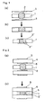
- Fig. 1 shows diagrammatic cross-sectional views showing an embodiment of a method of manufacturing a multilayer board according to the present invention, and showing a case of performing (a) filling a conductive paste 2 in a via hole of a pre-preg 1, (b) arranging copper layers 3 on both upper and lower surfaces of the pre-preg 1 and pressing for unifying the same, and (c) subsequently, performing patterning.
- Reference numeral 2' denotes a cured conductive paste
- reference numeral 3' denotes patterned copper layers.
- FIG. 2 shows diagrammatic cross-sectional views showing another embodiment of a method of manufacturing a multilayer board according to the present invention, and showing a case of performing (a) filling the conductive paste 2 in a via hole of the pre-preg 1, (b) arranging copper layer portions 5 of a patterned board 4 on both of the upper and lower surfaces of the pre-preg 1 so as to come into contact with the conductive paste and pressing for unifying the same.
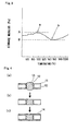
- the pre-preg used in the present invention is a pre-preg having a ratio A/B of 10 or higher before preheating, where A is a storage modulus at an inflection point e where the storage modulus changes from increasing to decreasing in a temperature profile rising from 60°C to 200°C and B is a storage modulus at an inflection point b where the storage modulus changes from decreasing to increasing as shown in Fig. 3 .
- A is a storage modulus at an inflection point e where the storage modulus changes from increasing to decreasing in a temperature profile rising from 60°C to 200°C
- B is a storage modulus at an inflection point b where the storage modulus changes from decreasing to increasing as shown in Fig. 3 .
- a normal rheometer for example, Modular Compact Rheometer (MCR) 300 manufactured by Anton Paar
- the material of the pre-preg is not specifically limited and those containing at least one of phenoxy resin, epoxy resin, bismaleimide-triazine resin (BT resin) used in the related art as a component may be used. Also, glass fiber fabric as a reinforcing material may be those used in the related art.
- the preheating may be performed by selecting conditions achieving the ratio A/B of lower than 10, which are different depending on the kinds of the resin and, normally on the order of 30 to 120 minutes at temperatures from 80 to 140°C. As regards the timing of the preheating, the shorter the time from the preheating to the pressing process, the more preferable.
- the method of performing the preheating is, although not specifically limited, preferably performed by placing the pre-preg between plates having smooth surfaces such as stainless.
- a period required to achieve the ratio A/B of 10 or lower may be confirmed in advance, and the pre-preg may be heated in an air oven or the like by being placed between the plates having smooth surfaces under the predetermined conditions confirmed in advance before the process of forming via holes in the laser beam machining.
- the via holes are provided after the preheating and, at this time, by employing the laser beam machining, a wall surface of the hole is cured to some extent, which also prevent the pre-preg and the paste resin from being mixed.
- the conductive paste used in the present invention may need only to be the one containing at least a resin component and metal powder, so that the resin component is cured and at least part of the metal powder is melted by being heated at a predetermined temperature, thereby causing the metal powders, or the metal powder and conductive end surfaces such as the copper layer or the patterned copper portion in contact thereto to alloy.
- the conductive paste preferably contains (B) 200 to 2200 parts of metal powder including at least two types of metals including a low melting-point metal and a high melting-point metal and (C) 0.5 to 40 parts of curing agent including 0.3 to 35 parts of phenol-based curing agent and (D) 0.3 to 80 parts of flux as essential ingredients.
- acrylate resin monomer examples include isoamyl acrylate, neopentyl glycol diacrylate, Trimethylolpropane triacrylate, ditrimethylolpropane tetraacrylate, phenyl glycidyl ether acrylate hexamethylene diisocyanate urethane pre-polymer, acrylic acid adduct of bisphenol A diglycidyl ether, ethylene glycol dimethacrylate, diethylene glycol dimethacrylate.
- the epoxy resin include bisphenol A epoxy resin, brominated epoxy resin, bisphenol F epoxy resin, novolac epoxy resin, alicyclic epoxy resin, glycidylamine epoxy resin, glycidyl ether epoxy resin, glycidylester epoxy resin, heterocyclic epoxy resin.
- the compounding ratio (weight %) between the acrylate resin and epoxy resin is preferably 5:95 to 95:5 and, more preferably, 20:80 to 80:20.
- the resin component (A) described above may be acrylate resin monomer and epoxy resin pre-polymer blended with at least one of resin components; alkyd resin, melamine resin, and xylene resin.
- Alkyd resin, melamine resin, and xylene resin are used as resin modifying agent and the invention is not limited thereto as long as the object is achieved.
- the compound proportion when blending the resin modifying agent as described above is preferably less than 40 weight %, preferably, less than 10 weight % of the total resin component (A).
- the metal powder may be of any type as long as it causes alloying by being heated, two or more types of metals including at least one type of low melting-point metal having a melting point of 180°C or lower and one type of high melting-point metal having a melting point of 800°C or higher are preferably contained.
- Examples of mode of existence of the two or more types of metals include mixture of a certain type of metal powder with metal powder of other types, a certain type of metal powder coated with another type of metal, and a mixture thereof.
- the metal composed of a single type of metal and an alloy composed of two or more types of metals may be used.
- the low melting-point metal include sole indium (melting point: 156°C) or an alloy having a melting point of 180°C or below, of two or more selected from tin (meltingpoint:231°C), lead (melting point: 327°C), bismuth (melting point:271°C) and indiums, and two or more types of alloys may also be used.
- the high melting-point metal include gold (melting point: 1064°C), silver (melting point: 961°C), copper (melting point: 1083°C), and nickel (melting point: 1455°C) or alloys containing at least two types of metals listed here and, two or more types of sole metals or alloys, and combination of sole metal and alloy may also be used.
- the shape of the metal powder is not limited, and types used in the related art such as dendrite, spherical, and scale type may be used.
- the particle diameter is not limited as well, it is normally on the order of 1 to 50 ⁇ m in average diameter.
- the compounding amount of the metal powder is preferably 200 to 2200 parts with respect to 100 parts of the resin component (A). Also, the compounding ratio (weight ratio, hereinafter) between low melting-point metal powder and high melting-point metal powder described above is preferably in the range of 8:2 to 2:8.
- the curing agent (C) contains phenol-based curing agent as an essential ingredient, and as other agents, imidazole-based curing agent, cationic curing agent, radical curing agent (polymerization initiator) may also be used.
- the amount of usage of the phenol-based curing agent is preferably 0.3 to 35 parts with respect to 100 parts of the resin component.
- the amounts of usage of the curing agents other than the phenol-based curing agent is preferably 0.2 to 35 parts with respect to 100 parts of resin and, preferably 0.5 to 40 parts as the entire curing agent.
- Examples of the phenol-based curing agent include novolac phenol and naphthol-based compound.
- Examples of imidazole-based curing agent include imidazole, 2-undecylimidazole, 2-heptadecylimidazole, 2-etylimidazole, 2-phenylimidazole, 2-etyl-4-methyl-imidazole, 1-cyanoethyl-2-undecylimidazole, and 2-phenylimidazole.
- Examples of cationic curing agent include onium compounds as represented by boron trifluoride amine salts, P-methoxybenzene diazonium hexafluoro phosphate, diphenyliodonium hexafluorophosphate, triphenylsulfonium, tetra-n-butyl phosphonium tetraphenylborate, tetra-n-butylphosphonium-o, o-diethyl phosphorodithioate.
- Examples of radical curing agent (polymerization initiator) include dicumyl peroxide, t-butyl cumyl peroxide, t-butyl hydroperoxide, cumene hydroperoxide.
- flux which is a component (D) has a function to facilitate alloying of the above-described metal powder, and examples include zinc chloride, lactic acid, citric acid, oleic acid, stearic acid, glutamic acid, benzoic acid, oxalic acid, glutamic acid hydrochloride, anilinium chloride, cetyl pyridine bromide, urea, triethanolamine, glycerine, hydrazine, and rosin.
- the amount of usage of the flux is preferably 0.3 to 80 parts with respect to 100 parts of the resin component.
- the conductive paste used in the present invention may be obtained by mixing above described components.
- Metalize Paste (MP series) manufactured by TATSUTA SYSTEM ELECTRONICS Co.,LTD. can be preferably used as those offered commercially.
- the multilayer board according to the present invention is obtained by heating and, simultaneously, pressing the preheated pre-preg after having filled with the conductive paste in the via holes thereof under the conditions corresponding to the used alloying paste. It is easy to join obtained multilayer boards each other by using the preheated pre-preg defined in the present invention to achieve further multi-layering. Since the multilayer board obtained by the present invention is superior in long-term reliability, and is superior in reliability of the joint portion of the multilayers, a super-multilayer board having several tens of layers, which used to be difficult to manufacture in the related art, can be manufactured with improved yield according to the present invention.
- a pre-preg (R-1551 manufactured by Panasonic Electric Works CO,Ltd. or GHPL-830 manufactured by Mitsubishi Gas Chemical Company, Inc.) having a thickness of approximately 100 ⁇ m shown in Table 1 was used. Preheating was performed in Examples 1 to 3, and Comparative example 3 as described below, and preheating was not performed in Comparative Examples 1 and 2. Holes of ⁇ 100 ⁇ m and ⁇ 150 ⁇ m were formed through the pre-preg using CO 2 laser, conductive paste shown in Table 1 was filled therein using a printing method, and then pressing was performed using a vacuum pressing machine under the following conditions.
- the pre-preg was placed between stainless plates having a thickness of 1.2 mm and was subjected to heating process in a thermostatic bath set to temperatures shown in Table 1 for periods shown in Table 1.
- a storage modulus A at an inflection point "a" where the storage modulus is changed from increasing to decreasing and a storage modulus B at an inflection point “b” where the storage modulus is changed from decreasing to increasing, in a temperature profile increasing from 60°C to 200°C, were measured before preheating and after preheating (except for Comparative Examples 1 and 2) respectively using Modular Compact Rheometer (MCR) 300 manufactured by Anton Paar, and the ratio A/B was obtained from these measured values.
- MCR Modular Compact Rheometer
- alloying paste or powder contact paste shown below was used as shown in Table 1. Alloying type: Metalize Paste (MP series) manufactured by TATSUTA SYSTEM ELECTRONICS Co., LTD. Powder Contact type: AE1840 manufactured by TATSUTA SYSTEM ELECTRONICS Co., LTD.
- a cross-sectional surface of a finished board was observed by an optical microscope and a swelling amount (s) shown in Fig. 6 was measured, and cases where the swelling amount was smaller than 5 ⁇ m were marked by circles, and cases where the swelling amount was 5 ⁇ m or larger was marked by crosses.
- Rate of change of conductivity was obtained by following expressions: b - a ⁇ 100 / a where a was a value of resistance measured before a test in a given manufactured connecting pattern, and b is a value of resistance measured after the test, and cases where the rate of change of conductivity was within ⁇ 20% were marked by circles, and cases where the rate of change of conductivity was below -20% or over 20% were marked by crosses.
- Solder Dip Test a cycle wherein immersed in solder at a temperature of 260°C for 10 seconds and then cooled by atmospheric air at a room temperature was repeated three times.
- Pressure Cooker Test (PCT) exposed to atmosphere at a temperature of 121°C, a humidity of 100%, and of 2 atmospheric pressure, for 24 hours.
- Heat Cycle Test a cycle wherein exposed in atmosphere held at -65° C for 30 minutes and then held at 125°C for 30 minutes was repeated 1000 times.
- Heat Resistance Test exposed in atmosphere of 100°C for 1000 hours.
- Humidity Resistance Test exposed in atmosphere of a temperature of 85°C and a humidity of 85% for 1000 hours.
- the conductive paste was filled in holes of ⁇ 150 ⁇ m and a comb shaped pattern including three hole pitches of 0.6 mm, 0.8 mm, and 1.0 mm was manufactured.
- a direct current 50V was applied on the pattern and, after having exposed to a temperature of 85°C, a humidity of 85% for 1000 hours, the value of resistance was measured still in a test atmosphere, and cases where the value of resistance was 10 6 ⁇ or lager were marked as "good", and cases of being smaller than 10 6 ⁇ were marked as "poor".
- Example 1 Example 2
- Example 3 Comparative Example 1 Comparative Example 2 Comparative Example 3 pre-preg R-1551 GHPL-830 R-1551 R-1551 GHPL-830 R-1551 preheating conditions 120°C/60min 120°C/60min 120°C/30min nil nil 120°C/60min storage modulus A/B before preheating 34.7 15.1 34.7 34.7 15.1 34.7 after preheating 4.1 2.1 9.1 - - 4.1 conductive paste alloying type alloying type alloying type alloying type alloying type powder contact type swelling after pressing good good good good good good poor initial conductivity (m ⁇ /1 hole) hole diameter ⁇ 0.15 5.1 5.3 7.4 94.8 5.7 6.6 ⁇ 0.10 6.5 7.5 9.5 447 10.9 390 rate of change after solder dip test (%) (260°C/10s ⁇ 3 cycles) hole diameter ⁇ 0.15 good good good good good good good good ⁇ 0.10 good good good good poor good poor rate of change after PCT (%) (121°C/100%RH/2
Landscapes
- Engineering & Computer Science (AREA)
- Microelectronics & Electronic Packaging (AREA)
- Manufacturing & Machinery (AREA)
- Physics & Mathematics (AREA)
- Chemical & Material Sciences (AREA)
- Dispersion Chemistry (AREA)
- Spectroscopy & Molecular Physics (AREA)
- Production Of Multi-Layered Print Wiring Board (AREA)
- Conductive Materials (AREA)
- Printing Elements For Providing Electric Connections Between Printed Circuits (AREA)
- Parts Printed On Printed Circuit Boards (AREA)
Abstract
Description
- The present invention relates to a method of manufacturing a multilayer wiring board and a multilayer wiring board obtained thereby and, more specifically, a method of manufacturing a multilayer wiring board in which via holes are filled with conductive paste containing metal powder.
- In recent years, in association with a trend toward reduction of thickness and length of products in the field of electronics, the similar needs are increasing also for a printed wiring board. Multi-layering is inevitable in miniaturization of the printed wiring board and, in order to achieve the multi-layering, reduction of thickness is a technical challenge.
- As a method of manufacturing the multilayer wiring board of the related art, there is a method including (a) providing a via hole on a
core board 10 havingcopper layer layers 11 on both surfaces of an insulated material, applying a through hole plating 12 on a wall surface of the via hole and then printing, filling and hardening via-fillpaste 13 therein, then (b) polishing projecting portions of the filledconductive paste 13, and then (c) applying cap plating 14 on the both surfaces, as shown inFig. 4 for example. There is also a method of filling a via hole by using a resin of aresin layer 15 of acore board 10 by disposing copper layers (CCL) 16 having alayer 15 applied with a resin on both sides of thecore board 10, with theresin layers 15 facing thecore board 10, as shown inFig. 5(a) , and pressing the same as shown in (b). - However, the former has a probability of extension of the board after having polished the paste and hence the reduction of the thickness of the film is limited, while the cap plating results in increase in thickness of the copper layers on the surfaces which causes a difficulty of fine patterning. In contrast, the latter has problems of an inability to provide a via hole on a via hole (stacked via), insufficient smoothness of the surface of the board, and generation of cracks at the time of a long-term reliability test.
- In cope with these problems, a method of obtaining an internal layer conductivity only with the conductive paste without performing the through hole plating or the cap plating as described above, more specifically, a press method using paste which develops conductivity by contact between conductive powder and conductive powder (hereinafter, referred to as powder contact paste) is employed. However, utilization of such paste causes a problem of generation of roughness because the board immediately above the paste is swelled under normal pressing conditions, and also causes a problem of insufficient long-term reliability because the change rate of conductivity over time is high.
- In contrast, the fact that the conductivity and the long-term stability can be improved by using paste containing metal powder which is alloyed by being heated (hereinafter referred to as "alloying paste") and forming alloy between the conductive powders and between the powder and the copper layer is disclosed (Patent Document 1).
- In contrast, pre-preg is generally used as a material of the printed board (Patent Document 2). The term "pre-preg" means an adhesive sheet obtained by processing thermosetting resin into a state of B-stage, and is normally a glass fiber cloth or the like as a reinforcing material impregnated with a thermosetting resin. When manufacturing the board using the pre-preg described above, a via hole is formed through the pre-preg by laser beam machining as in the related art, conductive paste is filled therein, copper layers or patterned boards are arranged on upper and lower surfaces thereof, and pressing is performed.
- However, when forming a through hole with the alloying paste described above, it is necessary to slow down a curing speed of the paste resin component because alloying is hindered if the paste resin component is completely cured before a low melting metal is melted. However, a general pre-preg has problems in that if the curing speed of the paste resin component is slowed down, the conductive paste may spread at the time of pressing, and the resin component of the pre-preg and the paste may be mixed, thereby failing to obtain desired characteristics.
-
- Patent Document 1: Japanese Patent No.
4191678 - Patent Document 2:
JP-A-7-176846 - In view of such circumstances as described above, it is an object of the present invention to provide a manufacturing method in which a multilayer printed wiring board (hereinafter, referred to as "multilayer board") superior in conductivity and long-term stability even when a general pre-preg, which is advantageous in terms of cost, is used, and a multilayer board obtained thereby.
- A method of manufacturing a multilayer board according to the present invention is a method of manufacturing a multilayer board including: a drilling step for forming a via hole through a pre-preg by laser beam machining, a step of filling the via hole with conductive paste containing a resin component and metal powder, and a step of arranging copper layers or copper layer portions of patterned boards on and under the filled conductive paste and pressing the same, characterized by using alloying paste as the conductive paste in which at least part of the metal powder is melted and the metal powders adjacent to each other are alloyed, using a pre-preg having a ratio of A divided by B of at least 10 before subjected to preheating, where A is a storage modulus at an inflection point where the storage modulus changes from increasing to decreasing and B is a storage modulus at an inflection point where the storage modulus changes from decreasing to increasing in a temperature profile rising from 60°C to 200°C, and preheating the pre-preg before the drilling step to reduce the ratio of A divided by B to below 10.
- In the description given above, a pre-preg containing at least one of phenoxy resin, epoxy resin, and bismaleimide-triazine resin (BT resin) is used as the pre-preg.
- Also, the preheating is performed normally at a temperature from 80 to 140°C for 30 to 120 minutes.
- Furthermore, it is preferable to use conductive paste having a following composition; (A) with respect to 100 weight parts of resin components containing acrylate resin monomer and epoxy resin pre-polymer, (B) 200 to 2200 parts of metal powder including at least one type of low melting-point metal having a melting point of 180°C or lower, being sole indium or an alloy of at least two types of metals selected from a group of tin, lead, bismuth, and indium, and a high melting-point metal selected from a group including gold, silver, copper and nickel and/or a high melting-point metal being an alloy having a melting point of 800°C or higher, obtained from two types of metals selected from the same group, (C) 0.5 to 40 weight parts of curing agent containing 0.3 to 35 weight parts of phenolic curing agent, and (D) 0.3 to 80 weight part of flux.
- The multilayer printed wiring board according to the present invention is a multilayer printed wiring board manufactured by forming a via hole through a pre-preg, filling the via hole with conductive paste, and arranging copper layers or copper layer portions of patterned boards on and under the filled conductive paste, using a pre-preg having a ratio of A to B below 10, where A is a storage modulus at an inflection point where the storage modulus changes from increasing to decreasing and B is a storage modulus at an inflection point where the storage modulus changes from decreasing to increasing in a temperature profile rising from 60°C to 200°C as the pre-preg, and using conductive paste containing metal powder including two or more types of metals which are alloyed with respect to each other by being heated as the conductive paste. The multilayer printed wiring board can be manufactured by the method of manufacturing according to the present invention described above.
- In the specification, "alloying" between metal powders means that two or more types of metals are melted and unified. It means, for example, when a substance including low melting-point metal particles and high melting-point metal particles mixed together is heated, surface layers of the respective particles are melted and unified, thereby forming an alloy layer.
- The multilayer board obtained by a method of manufacturing according to the present invention allows fine line patterning because a cap plating is not used, thereby satisfying the demand of reduction in thickness. Also, since the metal powders contained in the conductive paste are alloyed and the metal powder and end surfaces of the conductive layer in through holes are alloyed, so that superior conductivity and long-term stability are achieved. Also, since the problem of spreading or the like does not occur, a general pre-preg can be used, which is advantageous in terms of cost. Also, formation of a stacked via structure is possible. Furthermore, a super-multilayer board can be manufactured with higher yield by joining the multilayer board and the multilayer board. As described above, a high-quality multilayer board in which various problems of the related art are solved can be provided using a general apparatus at low cost.
-
- [
Fig. 1] Fig. 1 shows diagrammatic cross-sectional views showing an embodiment of a method of manufacturing a multilayer board according to the present invention. - [
Fig. 2] Fig. 2 shows diagrammatic cross-sectional views showing another embodiment of a method of manufacturing a multilayer board according to the present invention. - [
Fig. 3] Fig. 3 is a chart showing a result of measurement of storage modulus using a modular compact rheometer (MCR). - [
Fig. 4] Fig. 4 shows diagrammatic cross-sectional views showing an example of a method of manufacturing a multilayer board of the related art. - [
Fig. 5] Fig. 5 shows diagrammatic cross-sectional views showing another example of a method of manufacturing a multilayer board of the related art. - [
Fig. 6] Fig. 6 shows diagrammatic cross-sectional views showing a method of evaluating a swelling amount of the board. - A method of manufacturing a multilayer board according to the present invention includes at least (1) a process of preheating before providing via holes through a pre-preg, (2) a process of providing the via holes through the preheated pre-preg by laser beam machining, (3) a process of filling conductive paste in the via holes, (4) a process of arranging copper layers or copper layer portions of patterned boards on upper and lower surfaces of the filled conductive paste and pressing for unifying the same. In the process (3) described above, alloying paste containing metal powders melted by being heated at the time of curing of the paste wherein melted metal powders are alloyed with respect to each other is used as the conductive paste. In the process (4), if the copper layers which are not patterned are laminated, the patterning is performed after the pressing.
- Referring now to the drawings, description of the present invention will be given further in detail.
Fig. 1 shows diagrammatic cross-sectional views showing an embodiment of a method of manufacturing a multilayer board according to the present invention, and showing a case of performing (a) filling aconductive paste 2 in a via hole of a pre-preg 1, (b) arrangingcopper layers 3 on both upper and lower surfaces of the pre-preg 1 and pressing for unifying the same, and (c) subsequently, performing patterning. Reference numeral 2' denotes a cured conductive paste, and reference numeral 3' denotes patterned copper layers. - In contrast,
Fig. 2 shows diagrammatic cross-sectional views showing another embodiment of a method of manufacturing a multilayer board according to the present invention, and showing a case of performing (a) filling theconductive paste 2 in a via hole of the pre-preg 1, (b) arrangingcopper layer portions 5 of a patternedboard 4 on both of the upper and lower surfaces of the pre-preg 1 so as to come into contact with the conductive paste and pressing for unifying the same. - The pre-preg used in the present invention is a pre-preg having a ratio A/B of 10 or higher before preheating, where A is a storage modulus at an inflection point e where the storage modulus changes from increasing to decreasing in a temperature profile rising from 60°C to 200°C and B is a storage modulus at an inflection point b where the storage modulus changes from decreasing to increasing as shown in
Fig. 3 . For measuring the storage modulus of the pre-preg, a normal rheometer (for example, Modular Compact Rheometer (MCR) 300 manufactured by Anton Paar) may be used. - The material of the pre-preg is not specifically limited and those containing at least one of phenoxy resin, epoxy resin, bismaleimide-triazine resin (BT resin) used in the related art as a component may be used. Also, glass fiber fabric as a reinforcing material may be those used in the related art.
- The preheating may be performed by selecting conditions achieving the ratio A/B of lower than 10, which are different depending on the kinds of the resin and, normally on the order of 30 to 120 minutes at temperatures from 80 to 140°C. As regards the timing of the preheating, the shorter the time from the preheating to the pressing process, the more preferable. The method of performing the preheating is, although not specifically limited, preferably performed by placing the pre-preg between plates having smooth surfaces such as stainless.
- Therefore, a period required to achieve the ratio A/B of 10 or lower may be confirmed in advance, and the pre-preg may be heated in an air oven or the like by being placed between the plates having smooth surfaces under the predetermined conditions confirmed in advance before the process of forming via holes in the laser beam machining.
- The via holes are provided after the preheating and, at this time, by employing the laser beam machining, a wall surface of the hole is cured to some extent, which also prevent the pre-preg and the paste resin from being mixed.
- The conductive paste used in the present invention may need only to be the one containing at least a resin component and metal powder, so that the resin component is cured and at least part of the metal powder is melted by being heated at a predetermined temperature, thereby causing the metal powders, or the metal powder and conductive end surfaces such as the copper layer or the patterned copper portion in contact thereto to alloy.
- For example, with respect to (A) 100 weight parts (hereinafter, referred to simply as "parts") of resin components including acrylate resin monomer and epoxy resin pre-polymer, the conductive paste preferably contains (B) 200 to 2200 parts of metal powder including at least two types of metals including a low melting-point metal and a high melting-point metal and (C) 0.5 to 40 parts of curing agent including 0.3 to 35 parts of phenol-based curing agent and (D) 0.3 to 80 parts of flux as essential ingredients.
- Detailed examples of the acrylate resin monomer include isoamyl acrylate, neopentyl glycol diacrylate, Trimethylolpropane triacrylate, ditrimethylolpropane tetraacrylate, phenyl glycidyl ether acrylate hexamethylene diisocyanate urethane pre-polymer, acrylic acid adduct of bisphenol A diglycidyl ether, ethylene glycol dimethacrylate, diethylene glycol dimethacrylate.
- Detailed examples of the epoxy resin include bisphenol A epoxy resin, brominated epoxy resin, bisphenol F epoxy resin, novolac epoxy resin, alicyclic epoxy resin, glycidylamine epoxy resin, glycidyl ether epoxy resin, glycidylester epoxy resin, heterocyclic epoxy resin.
- The compounding ratio (weight %) between the acrylate resin and epoxy resin is preferably 5:95 to 95:5 and, more preferably, 20:80 to 80:20.
- The resin component (A) described above may be acrylate resin monomer and epoxy resin pre-polymer blended with at least one of resin components; alkyd resin, melamine resin, and xylene resin. Alkyd resin, melamine resin, and xylene resin are used as resin modifying agent and the invention is not limited thereto as long as the object is achieved. The compound proportion when blending the resin modifying agent as described above is preferably less than 40 weight %, preferably, less than 10 weight % of the total resin component (A).
- Although the metal powder may be of any type as long as it causes alloying by being heated, two or more types of metals including at least one type of low melting-point metal having a melting point of 180°C or lower and one type of high melting-point metal having a melting point of 800°C or higher are preferably contained. Examples of mode of existence of the two or more types of metals include mixture of a certain type of metal powder with metal powder of other types, a certain type of metal powder coated with another type of metal, and a mixture thereof.
- As the low melting-point metal and the high melting-point metal, the metal composed of a single type of metal and an alloy composed of two or more types of metals may be used.
- Preferable examples of the low melting-point metal include sole indium (melting point: 156°C) or an alloy having a melting point of 180°C or below, of two or more selected from tin (meltingpoint:231°C), lead (melting point: 327°C), bismuth (melting point:271°C) and indiums, and two or more types of alloys may also be used.
- Preferable examples of the high melting-point metal include gold (melting point: 1064°C), silver (melting point: 961°C), copper (melting point: 1083°C), and nickel (melting point: 1455°C) or alloys containing at least two types of metals listed here and, two or more types of sole metals or alloys, and combination of sole metal and alloy may also be used.
- Although the shape of the metal powder is not limited, and types used in the related art such as dendrite, spherical, and scale type may be used. Although the particle diameter is not limited as well, it is normally on the order of 1 to 50 µm in average diameter.
- The compounding amount of the metal powder is preferably 200 to 2200 parts with respect to 100 parts of the resin component (A). Also, the compounding ratio (weight ratio, hereinafter) between low melting-point metal powder and high melting-point metal powder described above is preferably in the range of 8:2 to 2:8.
- Subsequently, the curing agent (C) contains phenol-based curing agent as an essential ingredient, and as other agents, imidazole-based curing agent, cationic curing agent, radical curing agent (polymerization initiator) may also be used.
- The amount of usage of the phenol-based curing agent is preferably 0.3 to 35 parts with respect to 100 parts of the resin component. The amounts of usage of the curing agents other than the phenol-based curing agent is preferably 0.2 to 35 parts with respect to 100 parts of resin and, preferably 0.5 to 40 parts as the entire curing agent.
- Examples of the phenol-based curing agent include novolac phenol and naphthol-based compound. Examples of imidazole-based curing agent include imidazole, 2-undecylimidazole, 2-heptadecylimidazole, 2-etylimidazole, 2-phenylimidazole, 2-etyl-4-methyl-imidazole, 1-cyanoethyl-2-undecylimidazole, and 2-phenylimidazole. Examples of cationic curing agent include onium compounds as represented by boron trifluoride amine salts, P-methoxybenzene diazonium hexafluoro phosphate, diphenyliodonium hexafluorophosphate, triphenylsulfonium, tetra-n-butyl phosphonium tetraphenylborate, tetra-n-butylphosphonium-o, o-diethyl phosphorodithioate. Examples of radical curing agent (polymerization initiator) include dicumyl peroxide, t-butyl cumyl peroxide, t-butyl hydroperoxide, cumene hydroperoxide.
- Furthermore, flux, which is a component (D), has a function to facilitate alloying of the above-described metal powder, and examples include zinc chloride, lactic acid, citric acid, oleic acid, stearic acid, glutamic acid, benzoic acid, oxalic acid, glutamic acid hydrochloride, anilinium chloride, cetyl pyridine bromide, urea, triethanolamine, glycerine, hydrazine, and rosin. The amount of usage of the flux is preferably 0.3 to 80 parts with respect to 100 parts of the resin component.
- The conductive paste used in the present invention may be obtained by mixing above described components. However, for example, Metalize Paste (MP series) manufactured by TATSUTA SYSTEM ELECTRONICS Co.,LTD. can be preferably used as those offered commercially.
- The multilayer board according to the present invention is obtained by heating and, simultaneously, pressing the preheated pre-preg after having filled with the conductive paste in the via holes thereof under the conditions corresponding to the used alloying paste. It is easy to join obtained multilayer boards each other by using the preheated pre-preg defined in the present invention to achieve further multi-layering. Since the multilayer board obtained by the present invention is superior in long-term reliability, and is superior in reliability of the joint portion of the multilayers, a super-multilayer board having several tens of layers, which used to be difficult to manufacture in the related art, can be manufactured with improved yield according to the present invention.
- Although the present invention will be described further in detail with reference to examples, the present invention is not limited to the examples shown below.
- A pre-preg (R-1551 manufactured by Panasonic Electric Works CO,Ltd. or GHPL-830 manufactured by Mitsubishi Gas Chemical Company, Inc.) having a thickness of approximately 100 µm shown in Table 1 was used. Preheating was performed in Examples 1 to 3, and Comparative example 3 as described below, and preheating was not performed in Comparative Examples 1 and 2. Holes of φ100 µm and φ150 µm were formed through the pre-preg using CO2 laser, conductive paste shown in Table 1 was filled therein using a printing method, and then pressing was performed using a vacuum pressing machine under the following conditions.
- Pressure: 0kg/cm2 → surface pressure 10.2 kg/cm2 (pressure rising: 17 minutes, hold: 10 minutes) → surface pressure 30.6 kg/cm2 (pressure rising: 24 minutes, hold: 46 minutes) → 0kg/cm2 (pressure reduction: 23 minutes).
Temperature: 30°C → 130°C (temperature rising: 17 minutes, hold: 10 minutes) → 180°C (temperature rising: 24 minutes, hold: 46 minutes) → 30°C (cooling: 23 minutes). - As preheating of the pre-preg, the pre-preg was placed between stainless plates having a thickness of 1.2 mm and was subjected to heating process in a thermostatic bath set to temperatures shown in Table 1 for periods shown in Table 1.
- As regards the storage modulus of the pre-preg, a storage modulus A at an inflection point "a" where the storage modulus is changed from increasing to decreasing and a storage modulus B at an inflection point "b" where the storage modulus is changed from decreasing to increasing, in a temperature profile increasing from 60°C to 200°C, were measured before preheating and after preheating (except for Comparative Examples 1 and 2) respectively using Modular Compact Rheometer (MCR) 300 manufactured by Anton Paar, and the ratio A/B was obtained from these measured values.
- As the conductive paste, alloying paste or powder contact paste shown below was used as shown in Table 1.
Alloying type: Metalize Paste (MP series) manufactured by TATSUTA SYSTEM ELECTRONICS Co., LTD.
Powder Contact type: AE1840 manufactured by TATSUTA SYSTEM ELECTRONICS Co., LTD. - The following evaluations are performed on the multilayer board obtained by the procedure described above.
- A cross-sectional surface of a finished board was observed by an optical microscope and a swelling amount (s) shown in
Fig. 6 was measured, and cases where the swelling amount was smaller than 5 µm were marked by circles, and cases where the swelling amount was 5 µm or larger was marked by crosses. - As regards initial conductivity of φ0.15 mm, 200 holes, 400 holes, 600 holes, and 800 holes connecting patterns were manufactured and values of resistance were measured. The values of resistance were divided by respective numbers of holes to obtain the value of resistance per hole, and an average value was calculated. Manufacturing of the 200 holes, 400 holes, and 600 holes connecting patterns were performed with N=6, and manufacturing of the 800 holes connecting pattern was performed with N=2.
- As regards the initial conductivity of φ0.10 mm, 200 holes, 400 holes, and 600 holes connecting patterns were made and the values of resistance were measured. The values of resistance were divided by the respective numbers of holes to obtain the value of resistance per hole, and the average value was calculated. Manufacturing of the 200 holes, 400 holes, and 600 holes connecting patterns were performed with N=4.
- Rate of change of conductivity was obtained by following expressions:

where a was a value of resistance measured before a test in a given manufactured connecting pattern, and b is a value of resistance measured after the test, and cases where the rate of change of conductivity was within ± 20% were marked by circles, and cases where the rate of change of conductivity was below -20% or over 20% were marked by crosses. - Conditions of the long-term reliability test were as follows.
Solder Dip Test: a cycle wherein immersed in solder at a temperature of 260°C for 10 seconds and then cooled by atmospheric air at a room temperature was repeated three times.
Pressure Cooker Test (PCT) : exposed to atmosphere at a temperature of 121°C, a humidity of 100%, and of 2 atmospheric pressure, for 24 hours.
Heat Cycle Test: a cycle wherein exposed in atmosphere held at -65° C for 30 minutes and then held at 125°C for 30 minutes was repeated 1000 times.
Heat Resistance Test: exposed in atmosphere of 100°C for 1000 hours.
Humidity Resistance Test: exposed in atmosphere of a temperature of 85°C and a humidity of 85% for 1000 hours. - The conductive paste was filled in holes of φ150 µm and a comb shaped pattern including three hole pitches of 0.6 mm, 0.8 mm, and 1.0 mm was manufactured. A direct current 50V was applied on the pattern and, after having exposed to a temperature of 85°C, a humidity of 85% for 1000 hours, the value of resistance was measured still in a test atmosphere, and cases where the value of resistance was 106 Ω or lager were marked as "good", and cases of being smaller than 106 Ω were marked as "poor".
-
[Table 1] Example 1 Example 2 Example 3 Comparative Example 1 Comparative Example 2 Comparative Example 3 pre-preg R-1551 GHPL-830 R-1551 R-1551 GHPL-830 R-1551 preheating conditions 120°C/60min 120°C/60min 120°C/30min nil nil 120°C/60min storage modulus A/B before preheating 34.7 15.1 34.7 34.7 15.1 34.7 after preheating 4.1 2.1 9.1 - - 4.1 conductive paste alloying type alloying type alloying type alloying type alloying type powder contact type swelling after pressing good good good good good poor initial conductivity (mΩ/1 hole) hole diameter φ0.15 5.1 5.3 7.4 94.8 5.7 6.6 φ0.10 6.5 7.5 9.5 447 10.9 390 rate of change after solder dip test (%) (260°C/10s×3 cycles) hole diameter φ0.15 good good good good good good φ0.10 good good good poor good poor rate of change after PCT (%) (121°C/100%RH/2atm/24h) hole diameter φ0.15 good good good good good good rate of change of conductivity φ0.10 good good good poor good poor rate of change after heat cycle test (%) (-65°C 30m⇔125°C 30m/1000 cycles) hole diameter φ0.15 good good good good good good φ0.10 good good good good poor poor rate of change after heat resistance test (%) (100°C/1000h) hole diameter φ0.15 good good good good good good φ0.10 good good good good good poor rate of change after humidity resistance test (%) (85°C 85%RH/1000h) hole diameter φ0.15 good good good good good good φ0.10 good good good poor good poor insulation reliability (DC50V 85°C85%RH/1000h) hole diameter:φ 0.15 pitch P=1.0 good good good good good - P=0.8 good good good good good - P=0.6 good good good good good - - 1 ... pre-preg, 2 ... conductive paste, 3,5 ... copper layer, 4 ... patterned board,
10 ... core board, 11 ... copper layer, 12 ... through hole plating,
13 ... conductive paste, 14 ... cap plating, 15 ... resin layer, 16 ... copper layer
Claims (6)
- A method of manufacturing a multilayer printed wiring board, comprising: a drilling step for forming a via hole through a pre-preg by laser beam machining, a step of filling the via hole with conductive paste containing a resin component and metal powder, and a step of arranging copper layers or copper layer portions of patterned boards on and under the filled conductive paste and pressing the same, characterized by
using alloying paste as the conductive paste in which at least part of the metal powder is melted and the metal powders adjacent to each other are alloyed,
using a pre-preg having a ratio of A divided by B of at least 10 before subjected to preheating, where A is a storage modulus at an inflection point where the storage modulus changes from increasing to decreasing and B is a storage modulus at an inflection point where the storage modulus changes from decreasing to increasing in a temperature profile rising from 60°C to 200°C,
preheating the pre-preg before the drilling step to reduce the ratio of A divided by B to below 10. - The method of manufacturing a multilayer printed wiring board according to Claim 1, characterized by using a pre-preg containing at least one of phenoxy resin, epoxy resin, and bismaleimide-triazine resin as the pre-preg.
- The method of manufacturing a multilayer printed wiring board according to Claim 1 or 2, characterized in that the preheating is performed at a temperature from 80 to 140°C for 30 to 120 minutes.
- The method of manufacturing a multilayer printed wiring board according to any one of Claims 1 to 3, characterized by using the conductive paste having a following composition;(A) resin components containing acrylate resin monomer and epoxy resin pre-polymer, and with respect to 100 parts by weight of (A)(B) 200 to 2200 parts by weight of metal powder including at least one type of low melting-point metal having a melting point of 180°C or lower, being sole indium or an alloy of at least two types of metals selected from a group of tin, lead, bismuth and indium, and a high melting-point metal selected from a group including gold, silver, copper and nickel and/or a high melting-point metal having a melting point of 800°C or higher, being an alloy of two types or more of metals selected from the same group,(C) 0.5 to 40 parts by weight of curing agent containing 0.3 to 35 weight parts of phenolic curing agent, and(D) 0.3 to 80 parts by weight of flux.
- A multilayer printed wiring board manufactured by the method of manufacturing according to any one of Claims 1 to 4.
- A multilayer printed wiring board manufactured by forming a via hole through a pre-preg, filling the via hole with conductive paste, and arranging copper layers or copper layer portions of patterned boards on and under the filled conductive paste, characterized by:using a pre-preg having a ratio of A divided by B of below 10, where A is a storage modulus at an inflection point where the storage modulus changes from increasing to decreasing and B is a storage modulus at an inflection point where the storage modulus changes from decreasing to increasing in a temperature profile rising from 60°C to 200°C as the pre-preg, andusing conductive paste containing metal powder including two or more types of metals which are alloyed with each other by being heated.
Applications Claiming Priority (3)
| Application Number | Priority Date | Filing Date | Title |
|---|---|---|---|
| JP2009059375 | 2009-03-12 | ||
| JP2009171229 | 2009-07-22 | ||
| PCT/JP2010/001656 WO2010103805A1 (en) | 2009-03-12 | 2010-03-09 | Multilayer wiring substrate producing method and multilayer wiring substrate obtained by the same |
Publications (3)
| Publication Number | Publication Date |
|---|---|
| EP2408285A1 true EP2408285A1 (en) | 2012-01-18 |
| EP2408285A4 EP2408285A4 (en) | 2017-11-22 |
| EP2408285B1 EP2408285B1 (en) | 2018-11-14 |
Family
ID=42728101
Family Applications (1)
| Application Number | Title | Priority Date | Filing Date |
|---|---|---|---|
| EP10750562.0A Not-in-force EP2408285B1 (en) | 2009-03-12 | 2010-03-09 | Method of manufacturing multilayer printed wiring board and multilayer wiring board obtained thereby |
Country Status (7)
| Country | Link |
|---|---|
| US (2) | US8756805B2 (en) |
| EP (1) | EP2408285B1 (en) |
| JP (1) | JP4778114B2 (en) |
| KR (1) | KR101114058B1 (en) |
| CN (1) | CN102369791B (en) |
| TW (1) | TWI419633B (en) |
| WO (1) | WO2010103805A1 (en) |
Cited By (1)
| Publication number | Priority date | Publication date | Assignee | Title |
|---|---|---|---|---|
| EP2563103A4 (en) * | 2011-01-18 | 2013-05-15 | Panasonic Corp | CONNECTING SUBSTRATE, METHOD FOR MANUFACTURING CONNECTING SUBSTRATE, AND PULP FOR METALLIC HOLE |
Families Citing this family (8)
| Publication number | Priority date | Publication date | Assignee | Title |
|---|---|---|---|---|
| JP5693940B2 (en) | 2010-12-13 | 2015-04-01 | 株式会社トクヤマ | Ceramic via substrate, metallized ceramic via substrate, and manufacturing method thereof |
| KR20130066929A (en) * | 2011-12-13 | 2013-06-21 | 한국전자통신연구원 | Pattern forming composition and pattern forming method using the same |
| EP2796018A4 (en) * | 2011-12-21 | 2015-08-12 | Satinderpall S Pannu | METHOD FOR MANUFACTURING ELECTRICAL INTERFACE CONNECTIONS USING EXTRUDED METAL INTERCONNECTIONS |
| JP6464341B2 (en) * | 2014-10-30 | 2019-02-06 | 国立研究開発法人産業技術総合研究所 | Method for creating metal shaped object using metal powder by laser irradiation, forming material therefor, and created structure |
| US10263320B2 (en) * | 2015-07-17 | 2019-04-16 | Ohio State Innovation Foundation | Methods of making stretchable and flexible electronics |
| JP6803401B2 (en) * | 2016-12-28 | 2020-12-23 | タツタ電線株式会社 | Heat dissipation board, heat dissipation circuit configuration, and its manufacturing method |
| CN111491458A (en) * | 2019-01-25 | 2020-08-04 | 鹏鼎控股(深圳)股份有限公司 | Circuit board and manufacturing method thereof |
| WO2025254165A1 (en) * | 2024-06-04 | 2025-12-11 | 株式会社フジクラ | Printed wiring board |
Family Cites Families (22)
| Publication number | Priority date | Publication date | Assignee | Title |
|---|---|---|---|---|
| US4544801A (en) * | 1982-06-28 | 1985-10-01 | International Business Machines Corporation | Circuit board including multiple wire photosensitive adhesive |
| JPH04191678A (en) | 1990-11-27 | 1992-07-09 | Toshiba Corp | Apparatus for inspecting integrated circuit |
| US5403869A (en) * | 1992-08-17 | 1995-04-04 | Hitachi Chemical Company, Ltd. | Adhesive of epoxy resins, epoxy-modified polybutadiene and photoinitiator |
| JP2603053B2 (en) | 1993-10-29 | 1997-04-23 | 松下電器産業株式会社 | Conductor paste composition for filling via holes, double-sided and multilayer printed circuit boards using the same, and method for producing the same |
| CA2196024A1 (en) * | 1996-02-28 | 1997-08-28 | Craig N. Ernsberger | Multilayer electronic assembly utilizing a sinterable composition and related method of forming |
| JPH1072752A (en) * | 1996-05-15 | 1998-03-17 | Matsushita Electric Ind Co Ltd | Nonwoven fabric base material for printed wiring boards and prepreg using the same |
| JP2002232147A (en) | 2001-01-31 | 2002-08-16 | Purintekku:Kk | Multilayer wiring board and its producing method |
| JP2002329974A (en) * | 2001-05-01 | 2002-11-15 | Nitto Denko Corp | Wiring board and manufacturing method thereof |
| JP2004002789A (en) * | 2002-04-03 | 2004-01-08 | Sekisui Chem Co Ltd | Release film, laminated release film, and method of manufacturing substrate |
| KR100757163B1 (en) * | 2002-05-31 | 2007-09-07 | 다츠다 덴센 가부시키가이샤 | Conductive paste, multilayer board using the same and method for manufacturing same |
| JP2004158651A (en) * | 2002-11-06 | 2004-06-03 | Murata Mfg Co Ltd | Manufacturing method of resin substrate, resin multilayer substrate, and resin substrate |
| JP4747707B2 (en) * | 2004-11-09 | 2011-08-17 | ソニー株式会社 | Multilayer wiring board and board manufacturing method |
| CN101120623B (en) * | 2005-01-27 | 2010-07-28 | 松下电器产业株式会社 | Method for manufacturing multilayer circuit board and multilayer circuit board |
| KR100970063B1 (en) * | 2005-04-27 | 2010-07-16 | 히다치 가세고교 가부시끼가이샤 | Composites, prepregs, metal foil laminates, circuit board connection materials and multilayer printed wiring boards and methods for manufacturing the same |
| JP4689375B2 (en) | 2005-07-07 | 2011-05-25 | 富士通株式会社 | Laminated substrate and electronic device having the laminated substrate |
| TW200740334A (en) * | 2005-10-20 | 2007-10-16 | Matsushita Electric Industrial Co Ltd | Multilayer printed wiring board and its manufacturing method |
| WO2007069510A1 (en) * | 2005-12-12 | 2007-06-21 | Matsushita Electric Industrial Co., Ltd. | Intermediate material for manufacturing circuit board and method for manufacturing circuit board using such intermediate material |
| JP2007161797A (en) * | 2005-12-12 | 2007-06-28 | Matsushita Electric Ind Co Ltd | Prepreg characteristics test method |
| JP5109283B2 (en) * | 2006-04-20 | 2012-12-26 | パナソニック株式会社 | Circuit board manufacturing method |
| JP5214154B2 (en) * | 2007-01-19 | 2013-06-19 | 住友電気工業株式会社 | Printed wiring board and manufacturing method thereof |
| JP2008205111A (en) * | 2007-02-19 | 2008-09-04 | Fujitsu Ltd | Wiring board, semiconductor device, and manufacturing method of wiring board |
| JP4787195B2 (en) | 2007-03-26 | 2011-10-05 | 三菱樹脂株式会社 | Conductive paste composition for via hole filling and multilayer wiring board using the same |
-
2010
- 2010-03-09 KR KR1020117021603A patent/KR101114058B1/en active Active
- 2010-03-09 US US13/256,114 patent/US8756805B2/en active Active
- 2010-03-09 EP EP10750562.0A patent/EP2408285B1/en not_active Not-in-force
- 2010-03-09 CN CN2010800115999A patent/CN102369791B/en active Active
- 2010-03-09 WO PCT/JP2010/001656 patent/WO2010103805A1/en not_active Ceased
- 2010-03-09 JP JP2010525547A patent/JP4778114B2/en active Active
- 2010-03-10 TW TW099106904A patent/TWI419633B/en active
-
2014
- 2014-01-27 US US14/164,900 patent/US9420706B2/en active Active
Non-Patent Citations (1)
| Title |
|---|
| See references of WO2010103805A1 * |
Cited By (1)
| Publication number | Priority date | Publication date | Assignee | Title |
|---|---|---|---|---|
| EP2563103A4 (en) * | 2011-01-18 | 2013-05-15 | Panasonic Corp | CONNECTING SUBSTRATE, METHOD FOR MANUFACTURING CONNECTING SUBSTRATE, AND PULP FOR METALLIC HOLE |
Also Published As
| Publication number | Publication date |
|---|---|
| JP4778114B2 (en) | 2011-09-21 |
| US9420706B2 (en) | 2016-08-16 |
| KR20110112877A (en) | 2011-10-13 |
| HK1167776A1 (en) | 2012-12-07 |
| EP2408285B1 (en) | 2018-11-14 |
| WO2010103805A1 (en) | 2010-09-16 |
| JPWO2010103805A1 (en) | 2012-09-13 |
| CN102369791A (en) | 2012-03-07 |
| TWI419633B (en) | 2013-12-11 |
| US8756805B2 (en) | 2014-06-24 |
| KR101114058B1 (en) | 2012-03-13 |
| CN102369791B (en) | 2013-11-13 |
| EP2408285A4 (en) | 2017-11-22 |
| US20120037409A1 (en) | 2012-02-16 |
| US20140138126A1 (en) | 2014-05-22 |
| TW201043109A (en) | 2010-12-01 |
Similar Documents
| Publication | Publication Date | Title |
|---|---|---|
| EP2408285B1 (en) | Method of manufacturing multilayer printed wiring board and multilayer wiring board obtained thereby | |
| JP4191678B2 (en) | Conductive paste, multilayer substrate using the same, and manufacturing method thereof | |
| JP5333701B1 (en) | Wiring board and manufacturing method thereof | |
| JP5333702B1 (en) | Flexible wiring board, manufacturing method thereof, mounted product using the same, and flexible multilayer wiring board | |
| TWI393496B (en) | Wiring board, method of manufacturing wiring board, and via paste | |
| WO2004077560A1 (en) | Multilayer printed wiring board | |
| CN110088895B (en) | Heat dissipation base material, heat dissipation circuit structure and manufacturing method thereof | |
| JP4468750B2 (en) | Conductive paste and multilayer substrate using the same | |
| JP4949802B2 (en) | Conductive paste and multilayer substrate using the same | |
| JP3415756B2 (en) | Paste for filling through hole and printed wiring board using the same | |
| JP4109156B2 (en) | Conductive paste | |
| WO2023282351A1 (en) | Conductive paste and multilayer substrate using same | |
| JP3683506B2 (en) | Process for producing conductive paste composition for via filling | |
| HK1167776B (en) | Multilayer wiring substrate producing method and multilayer wiring substrate obtained by the same | |
| WO2013099204A1 (en) | Wiring board and manufacturing method therefor |
Legal Events
| Date | Code | Title | Description |
|---|---|---|---|
| PUAI | Public reference made under article 153(3) epc to a published international application that has entered the european phase |
Free format text: ORIGINAL CODE: 0009012 |
|
| 17P | Request for examination filed |
Effective date: 20110927 |
|
| AK | Designated contracting states |
Kind code of ref document: A1 Designated state(s): AT BE BG CH CY CZ DE DK EE ES FI FR GB GR HR HU IE IS IT LI LT LU LV MC MK MT NL NO PL PT RO SE SI SK SM TR |
|
| DAX | Request for extension of the european patent (deleted) | ||
| RA4 | Supplementary search report drawn up and despatched (corrected) |
Effective date: 20171020 |
|
| RIC1 | Information provided on ipc code assigned before grant |
Ipc: H05K 3/40 20060101ALI20171016BHEP Ipc: H01B 1/22 20060101ALI20171016BHEP Ipc: H05K 1/09 20060101ALI20171016BHEP Ipc: H05K 3/46 20060101AFI20171016BHEP Ipc: H05K 3/00 20060101ALN20171016BHEP |
|
| GRAP | Despatch of communication of intention to grant a patent |
Free format text: ORIGINAL CODE: EPIDOSNIGR1 |
|
| STAA | Information on the status of an ep patent application or granted ep patent |
Free format text: STATUS: GRANT OF PATENT IS INTENDED |
|
| RIC1 | Information provided on ipc code assigned before grant |
Ipc: H01B 1/22 20060101ALI20180503BHEP Ipc: H05K 3/00 20060101ALN20180503BHEP Ipc: H05K 3/40 20060101ALI20180503BHEP Ipc: H05K 1/09 20060101ALI20180503BHEP Ipc: H05K 3/46 20060101AFI20180503BHEP |
|
| INTG | Intention to grant announced |
Effective date: 20180528 |
|
| RIN1 | Information on inventor provided before grant (corrected) |
Inventor name: YUKAWA, KEN Inventor name: UMEDA, HIROAKI Inventor name: YAMAGUCHI, NORIHIRO |
|
| GRAS | Grant fee paid |
Free format text: ORIGINAL CODE: EPIDOSNIGR3 |
|
| GRAA | (expected) grant |
Free format text: ORIGINAL CODE: 0009210 |
|
| STAA | Information on the status of an ep patent application or granted ep patent |
Free format text: STATUS: THE PATENT HAS BEEN GRANTED |
|
| AK | Designated contracting states |
Kind code of ref document: B1 Designated state(s): AT BE BG CH CY CZ DE DK EE ES FI FR GB GR HR HU IE IS IT LI LT LU LV MC MK MT NL NO PL PT RO SE SI SK SM TR |
|
| REG | Reference to a national code |
Ref country code: GB Ref legal event code: FG4D |
|
| REG | Reference to a national code |
Ref country code: CH Ref legal event code: EP Ref country code: AT Ref legal event code: REF Ref document number: 1066395 Country of ref document: AT Kind code of ref document: T Effective date: 20181115 |
|
| REG | Reference to a national code |
Ref country code: DE Ref legal event code: R096 Ref document number: 602010055096 Country of ref document: DE |
|
| REG | Reference to a national code |
Ref country code: IE Ref legal event code: FG4D |
|
| REG | Reference to a national code |
Ref country code: NL Ref legal event code: MP Effective date: 20181114 |
|
| REG | Reference to a national code |
Ref country code: LT Ref legal event code: MG4D |
|
| REG | Reference to a national code |
Ref country code: AT Ref legal event code: MK05 Ref document number: 1066395 Country of ref document: AT Kind code of ref document: T Effective date: 20181114 |
|
| PG25 | Lapsed in a contracting state [announced via postgrant information from national office to epo] |
Ref country code: FI Free format text: LAPSE BECAUSE OF FAILURE TO SUBMIT A TRANSLATION OF THE DESCRIPTION OR TO PAY THE FEE WITHIN THE PRESCRIBED TIME-LIMIT Effective date: 20181114 Ref country code: IS Free format text: LAPSE BECAUSE OF FAILURE TO SUBMIT A TRANSLATION OF THE DESCRIPTION OR TO PAY THE FEE WITHIN THE PRESCRIBED TIME-LIMIT Effective date: 20190314 Ref country code: HR Free format text: LAPSE BECAUSE OF FAILURE TO SUBMIT A TRANSLATION OF THE DESCRIPTION OR TO PAY THE FEE WITHIN THE PRESCRIBED TIME-LIMIT Effective date: 20181114 Ref country code: NO Free format text: LAPSE BECAUSE OF FAILURE TO SUBMIT A TRANSLATION OF THE DESCRIPTION OR TO PAY THE FEE WITHIN THE PRESCRIBED TIME-LIMIT Effective date: 20190214 Ref country code: BG Free format text: LAPSE BECAUSE OF FAILURE TO SUBMIT A TRANSLATION OF THE DESCRIPTION OR TO PAY THE FEE WITHIN THE PRESCRIBED TIME-LIMIT Effective date: 20190214 Ref country code: LT Free format text: LAPSE BECAUSE OF FAILURE TO SUBMIT A TRANSLATION OF THE DESCRIPTION OR TO PAY THE FEE WITHIN THE PRESCRIBED TIME-LIMIT Effective date: 20181114 Ref country code: ES Free format text: LAPSE BECAUSE OF FAILURE TO SUBMIT A TRANSLATION OF THE DESCRIPTION OR TO PAY THE FEE WITHIN THE PRESCRIBED TIME-LIMIT Effective date: 20181114 Ref country code: LV Free format text: LAPSE BECAUSE OF FAILURE TO SUBMIT A TRANSLATION OF THE DESCRIPTION OR TO PAY THE FEE WITHIN THE PRESCRIBED TIME-LIMIT Effective date: 20181114 Ref country code: AT Free format text: LAPSE BECAUSE OF FAILURE TO SUBMIT A TRANSLATION OF THE DESCRIPTION OR TO PAY THE FEE WITHIN THE PRESCRIBED TIME-LIMIT Effective date: 20181114 |
|
| PG25 | Lapsed in a contracting state [announced via postgrant information from national office to epo] |
Ref country code: PT Free format text: LAPSE BECAUSE OF FAILURE TO SUBMIT A TRANSLATION OF THE DESCRIPTION OR TO PAY THE FEE WITHIN THE PRESCRIBED TIME-LIMIT Effective date: 20190314 Ref country code: NL Free format text: LAPSE BECAUSE OF FAILURE TO SUBMIT A TRANSLATION OF THE DESCRIPTION OR TO PAY THE FEE WITHIN THE PRESCRIBED TIME-LIMIT Effective date: 20181114 Ref country code: SE Free format text: LAPSE BECAUSE OF FAILURE TO SUBMIT A TRANSLATION OF THE DESCRIPTION OR TO PAY THE FEE WITHIN THE PRESCRIBED TIME-LIMIT Effective date: 20181114 Ref country code: GR Free format text: LAPSE BECAUSE OF FAILURE TO SUBMIT A TRANSLATION OF THE DESCRIPTION OR TO PAY THE FEE WITHIN THE PRESCRIBED TIME-LIMIT Effective date: 20190215 |
|
| PG25 | Lapsed in a contracting state [announced via postgrant information from national office to epo] |
Ref country code: IT Free format text: LAPSE BECAUSE OF FAILURE TO SUBMIT A TRANSLATION OF THE DESCRIPTION OR TO PAY THE FEE WITHIN THE PRESCRIBED TIME-LIMIT Effective date: 20181114 Ref country code: DK Free format text: LAPSE BECAUSE OF FAILURE TO SUBMIT A TRANSLATION OF THE DESCRIPTION OR TO PAY THE FEE WITHIN THE PRESCRIBED TIME-LIMIT Effective date: 20181114 Ref country code: PL Free format text: LAPSE BECAUSE OF FAILURE TO SUBMIT A TRANSLATION OF THE DESCRIPTION OR TO PAY THE FEE WITHIN THE PRESCRIBED TIME-LIMIT Effective date: 20181114 Ref country code: CZ Free format text: LAPSE BECAUSE OF FAILURE TO SUBMIT A TRANSLATION OF THE DESCRIPTION OR TO PAY THE FEE WITHIN THE PRESCRIBED TIME-LIMIT Effective date: 20181114 |
|
| REG | Reference to a national code |
Ref country code: DE Ref legal event code: R097 Ref document number: 602010055096 Country of ref document: DE |
|
| PG25 | Lapsed in a contracting state [announced via postgrant information from national office to epo] |
Ref country code: RO Free format text: LAPSE BECAUSE OF FAILURE TO SUBMIT A TRANSLATION OF THE DESCRIPTION OR TO PAY THE FEE WITHIN THE PRESCRIBED TIME-LIMIT Effective date: 20181114 Ref country code: SK Free format text: LAPSE BECAUSE OF FAILURE TO SUBMIT A TRANSLATION OF THE DESCRIPTION OR TO PAY THE FEE WITHIN THE PRESCRIBED TIME-LIMIT Effective date: 20181114 Ref country code: SM Free format text: LAPSE BECAUSE OF FAILURE TO SUBMIT A TRANSLATION OF THE DESCRIPTION OR TO PAY THE FEE WITHIN THE PRESCRIBED TIME-LIMIT Effective date: 20181114 Ref country code: EE Free format text: LAPSE BECAUSE OF FAILURE TO SUBMIT A TRANSLATION OF THE DESCRIPTION OR TO PAY THE FEE WITHIN THE PRESCRIBED TIME-LIMIT Effective date: 20181114 |
|
| PLBE | No opposition filed within time limit |
Free format text: ORIGINAL CODE: 0009261 |
|
| STAA | Information on the status of an ep patent application or granted ep patent |
Free format text: STATUS: NO OPPOSITION FILED WITHIN TIME LIMIT |
|
| 26N | No opposition filed |
Effective date: 20190815 |
|
| PG25 | Lapsed in a contracting state [announced via postgrant information from national office to epo] |
Ref country code: SI Free format text: LAPSE BECAUSE OF FAILURE TO SUBMIT A TRANSLATION OF THE DESCRIPTION OR TO PAY THE FEE WITHIN THE PRESCRIBED TIME-LIMIT Effective date: 20181114 Ref country code: MC Free format text: LAPSE BECAUSE OF FAILURE TO SUBMIT A TRANSLATION OF THE DESCRIPTION OR TO PAY THE FEE WITHIN THE PRESCRIBED TIME-LIMIT Effective date: 20181114 |
|
| REG | Reference to a national code |
Ref country code: CH Ref legal event code: PL |
|
| GBPC | Gb: european patent ceased through non-payment of renewal fee |
Effective date: 20190309 |
|
| PG25 | Lapsed in a contracting state [announced via postgrant information from national office to epo] |
Ref country code: LU Free format text: LAPSE BECAUSE OF NON-PAYMENT OF DUE FEES Effective date: 20190309 |
|
| REG | Reference to a national code |
Ref country code: BE Ref legal event code: MM Effective date: 20190331 |
|
| PG25 | Lapsed in a contracting state [announced via postgrant information from national office to epo] |
Ref country code: IE Free format text: LAPSE BECAUSE OF NON-PAYMENT OF DUE FEES Effective date: 20190309 Ref country code: LI Free format text: LAPSE BECAUSE OF NON-PAYMENT OF DUE FEES Effective date: 20190331 Ref country code: CH Free format text: LAPSE BECAUSE OF NON-PAYMENT OF DUE FEES Effective date: 20190331 Ref country code: GB Free format text: LAPSE BECAUSE OF NON-PAYMENT OF DUE FEES Effective date: 20190309 |
|
| PG25 | Lapsed in a contracting state [announced via postgrant information from national office to epo] |
Ref country code: BE Free format text: LAPSE BECAUSE OF NON-PAYMENT OF DUE FEES Effective date: 20190331 |
|
| PG25 | Lapsed in a contracting state [announced via postgrant information from national office to epo] |
Ref country code: TR Free format text: LAPSE BECAUSE OF FAILURE TO SUBMIT A TRANSLATION OF THE DESCRIPTION OR TO PAY THE FEE WITHIN THE PRESCRIBED TIME-LIMIT Effective date: 20181114 |
|
| PG25 | Lapsed in a contracting state [announced via postgrant information from national office to epo] |
Ref country code: MT Free format text: LAPSE BECAUSE OF NON-PAYMENT OF DUE FEES Effective date: 20190309 |
|
| PG25 | Lapsed in a contracting state [announced via postgrant information from national office to epo] |
Ref country code: CY Free format text: LAPSE BECAUSE OF FAILURE TO SUBMIT A TRANSLATION OF THE DESCRIPTION OR TO PAY THE FEE WITHIN THE PRESCRIBED TIME-LIMIT Effective date: 20181114 |
|
| PG25 | Lapsed in a contracting state [announced via postgrant information from national office to epo] |
Ref country code: HU Free format text: LAPSE BECAUSE OF FAILURE TO SUBMIT A TRANSLATION OF THE DESCRIPTION OR TO PAY THE FEE WITHIN THE PRESCRIBED TIME-LIMIT; INVALID AB INITIO Effective date: 20100309 |
|
| PG25 | Lapsed in a contracting state [announced via postgrant information from national office to epo] |
Ref country code: MK Free format text: LAPSE BECAUSE OF FAILURE TO SUBMIT A TRANSLATION OF THE DESCRIPTION OR TO PAY THE FEE WITHIN THE PRESCRIBED TIME-LIMIT Effective date: 20181114 |
|
| PGFP | Annual fee paid to national office [announced via postgrant information from national office to epo] |
Ref country code: FR Payment date: 20230324 Year of fee payment: 14 |
|
| PGFP | Annual fee paid to national office [announced via postgrant information from national office to epo] |
Ref country code: DE Payment date: 20220620 Year of fee payment: 14 |
|
| P01 | Opt-out of the competence of the unified patent court (upc) registered |
Effective date: 20230411 |
|
| REG | Reference to a national code |
Ref country code: DE Ref legal event code: R119 Ref document number: 602010055096 Country of ref document: DE |
|
| PG25 | Lapsed in a contracting state [announced via postgrant information from national office to epo] |
Ref country code: DE Free format text: LAPSE BECAUSE OF NON-PAYMENT OF DUE FEES Effective date: 20241001 |
|
| PG25 | Lapsed in a contracting state [announced via postgrant information from national office to epo] |
Ref country code: FR Free format text: LAPSE BECAUSE OF NON-PAYMENT OF DUE FEES Effective date: 20240331 |
|
| PG25 | Lapsed in a contracting state [announced via postgrant information from national office to epo] |
Ref country code: FR Free format text: LAPSE BECAUSE OF NON-PAYMENT OF DUE FEES Effective date: 20240331 Ref country code: DE Free format text: LAPSE BECAUSE OF NON-PAYMENT OF DUE FEES Effective date: 20241001 |