EP2408038A2 - Organic light-emitting apparatus and method of manufacturing the same - Google Patents
Organic light-emitting apparatus and method of manufacturing the same Download PDFInfo
- Publication number
- EP2408038A2 EP2408038A2 EP11173649A EP11173649A EP2408038A2 EP 2408038 A2 EP2408038 A2 EP 2408038A2 EP 11173649 A EP11173649 A EP 11173649A EP 11173649 A EP11173649 A EP 11173649A EP 2408038 A2 EP2408038 A2 EP 2408038A2
- Authority
- EP
- European Patent Office
- Prior art keywords
- electrode
- sealing member
- device substrate
- organic light
- layer
- Prior art date
- Legal status (The legal status is an assumption and is not a legal conclusion. Google has not performed a legal analysis and makes no representation as to the accuracy of the status listed.)
- Granted
Links
Images



Classifications
-
- H—ELECTRICITY
- H10—SEMICONDUCTOR DEVICES; ELECTRIC SOLID-STATE DEVICES NOT OTHERWISE PROVIDED FOR
- H10K—ORGANIC ELECTRIC SOLID-STATE DEVICES
- H10K59/00—Integrated devices, or assemblies of multiple devices, comprising at least one organic light-emitting element covered by group H10K50/00
- H10K59/10—OLED displays
-
- H—ELECTRICITY
- H10—SEMICONDUCTOR DEVICES; ELECTRIC SOLID-STATE DEVICES NOT OTHERWISE PROVIDED FOR
- H10K—ORGANIC ELECTRIC SOLID-STATE DEVICES
- H10K50/00—Organic light-emitting devices
- H10K50/80—Constructional details
- H10K50/84—Passivation; Containers; Encapsulations
- H10K50/842—Containers
- H10K50/8426—Peripheral sealing arrangements, e.g. adhesives, sealants
-
- H—ELECTRICITY
- H10—SEMICONDUCTOR DEVICES; ELECTRIC SOLID-STATE DEVICES NOT OTHERWISE PROVIDED FOR
- H10K—ORGANIC ELECTRIC SOLID-STATE DEVICES
- H10K59/00—Integrated devices, or assemblies of multiple devices, comprising at least one organic light-emitting element covered by group H10K50/00
- H10K59/80—Constructional details
- H10K59/87—Passivation; Containers; Encapsulations
- H10K59/871—Self-supporting sealing arrangements
- H10K59/8722—Peripheral sealing arrangements, e.g. adhesives, sealants
-
- H—ELECTRICITY
- H10—SEMICONDUCTOR DEVICES; ELECTRIC SOLID-STATE DEVICES NOT OTHERWISE PROVIDED FOR
- H10K—ORGANIC ELECTRIC SOLID-STATE DEVICES
- H10K85/00—Organic materials used in the body or electrodes of devices covered by this subclass
- H10K85/30—Coordination compounds
- H10K85/341—Transition metal complexes, e.g. Ru(II)polypyridine complexes
- H10K85/342—Transition metal complexes, e.g. Ru(II)polypyridine complexes comprising iridium
-
- H—ELECTRICITY
- H10—SEMICONDUCTOR DEVICES; ELECTRIC SOLID-STATE DEVICES NOT OTHERWISE PROVIDED FOR
- H10K—ORGANIC ELECTRIC SOLID-STATE DEVICES
- H10K85/00—Organic materials used in the body or electrodes of devices covered by this subclass
- H10K85/30—Coordination compounds
- H10K85/341—Transition metal complexes, e.g. Ru(II)polypyridine complexes
- H10K85/346—Transition metal complexes, e.g. Ru(II)polypyridine complexes comprising platinum
-
- H—ELECTRICITY
- H10—SEMICONDUCTOR DEVICES; ELECTRIC SOLID-STATE DEVICES NOT OTHERWISE PROVIDED FOR
- H10K—ORGANIC ELECTRIC SOLID-STATE DEVICES
- H10K85/00—Organic materials used in the body or electrodes of devices covered by this subclass
- H10K85/60—Organic compounds having low molecular weight
- H10K85/615—Polycyclic condensed aromatic hydrocarbons, e.g. anthracene
- H10K85/622—Polycyclic condensed aromatic hydrocarbons, e.g. anthracene containing four rings, e.g. pyrene
-
- H—ELECTRICITY
- H10—SEMICONDUCTOR DEVICES; ELECTRIC SOLID-STATE DEVICES NOT OTHERWISE PROVIDED FOR
- H10K—ORGANIC ELECTRIC SOLID-STATE DEVICES
- H10K85/00—Organic materials used in the body or electrodes of devices covered by this subclass
- H10K85/60—Organic compounds having low molecular weight
- H10K85/615—Polycyclic condensed aromatic hydrocarbons, e.g. anthracene
- H10K85/626—Polycyclic condensed aromatic hydrocarbons, e.g. anthracene containing more than one polycyclic condensed aromatic rings, e.g. bis-anthracene
-
- H—ELECTRICITY
- H10—SEMICONDUCTOR DEVICES; ELECTRIC SOLID-STATE DEVICES NOT OTHERWISE PROVIDED FOR
- H10K—ORGANIC ELECTRIC SOLID-STATE DEVICES
- H10K85/00—Organic materials used in the body or electrodes of devices covered by this subclass
- H10K85/60—Organic compounds having low molecular weight
- H10K85/649—Aromatic compounds comprising a hetero atom
- H10K85/654—Aromatic compounds comprising a hetero atom comprising only nitrogen as heteroatom
-
- H—ELECTRICITY
- H10—SEMICONDUCTOR DEVICES; ELECTRIC SOLID-STATE DEVICES NOT OTHERWISE PROVIDED FOR
- H10K—ORGANIC ELECTRIC SOLID-STATE DEVICES
- H10K85/00—Organic materials used in the body or electrodes of devices covered by this subclass
- H10K85/60—Organic compounds having low molecular weight
- H10K85/649—Aromatic compounds comprising a hetero atom
- H10K85/657—Polycyclic condensed heteroaromatic hydrocarbons
- H10K85/6572—Polycyclic condensed heteroaromatic hydrocarbons comprising only nitrogen in the heteroaromatic polycondensed ring system, e.g. phenanthroline or carbazole
-
- H—ELECTRICITY
- H10—SEMICONDUCTOR DEVICES; ELECTRIC SOLID-STATE DEVICES NOT OTHERWISE PROVIDED FOR
- H10K—ORGANIC ELECTRIC SOLID-STATE DEVICES
- H10K2102/00—Constructional details relating to the organic devices covered by this subclass
- H10K2102/10—Transparent electrodes, e.g. using graphene
- H10K2102/101—Transparent electrodes, e.g. using graphene comprising transparent conductive oxides [TCO]
- H10K2102/103—Transparent electrodes, e.g. using graphene comprising transparent conductive oxides [TCO] comprising indium oxides, e.g. ITO
Definitions
- An organic light-emitting apparatus and a method of manufacturing the same are provided.
- Organic light-emitting devices which are self-emitting devices, have advantages such as a wide viewing angle, excellent contrast, quick response, high brightness, and excellent driving voltage characteristics, and may provide multicolor images.
- an organic light-emitting device may include an anode, a cathode, and an organic layer disposed between the anode and the cathode.
- the organic layer may include a hole transport layer (HTL), an emission layer (EML), an electron transport layer (ETL), and a cathode.
- HTL hole transport layer
- EML emission layer
- ETL electron transport layer
- a cathode When a voltage is applied between the anode and the cathode, holes injected from the anode move to the EML via the HTL, and electrons injected from the cathode move to the EML via the ETL. Carriers such as the holes and electrons recombine in the EML to generate excitons. When the excitons drop from an excited state to a ground state, light is emitted.
- An organic light-emitting apparatus including the organic light-emitting device may further include a driving transistor or a switching transistor.
- a sealing unit for effectively sealing the organic light-emitting device is required in order to realize a high quality organic light-emitting apparatus.
- An organic light-emitting apparatus having a structure for preventing oxygen and/or moisture permeation is provided.
- a method of manufacturing the organic light-emitting apparatus is also provided.
- an organic light-emitting apparatus including: a device substrate including a light-emitting area and a non-emitting area; an encapsulation substrate covering the light-emitting area; a first electrode formed on the light-emitting area and disposed between the device substrate and the encapsulation substrate; an organic layer disposed between the encapsulation substrate and the first electrode; a second electrode disposed between the organic layer and the encapsulation substrate; a sealing member surrounding the light-emitting area; and a third electrode disposed on the non-emitting area outside the sealing member, including a first portion surrounding the sealing member, and comprising a same material as that of the first electrode.
- Each of the first electrode and the third electrode may preferably include at least one material selected from the group consisting of metals and conductive oxides.
- Each of the first electrode and the third electrode may preferably comprise indium tin oxide (ITO).
- ITO indium tin oxide
- the sealing member may preferably include at least one of an adhesive and glass frit.
- the sealing member may preferably include at least one of a silicon-based compound represented by Formula 1 and a cured product of the silicon-based compound: ⁇ Formula 1> F-[Q 1 ] a -O-[Q 2 -O] b -[-Q 3 -O] c -[Q 4 -O] d -[Q 5 ] e -[Y 1 ] f -Si(Z 1 ) g (Z 2 ) 3-g .
- the sealing member may preferably sequentially include a first sealing member layer, a second sealing member layer, and a third sealing member layer, each of the first sealing member layer and the third sealing member layer may include an adhesive, and the second sealing member layer may include at least one of the silicon-based compound represented by Formula 1 and the cured product of the silicon-based compound; A side surface of the sealing member and a side surface of the first portion of the third electrode may preferably contact each other.
- a maximum thickness of the first portion of the third electrode is L 2 and a maximum thickness of the sealing member is L 3 , preferably L 2 ⁇ L 3 .
- this may be a vacuum space.
- the organic light-emitting apparatus may preferably further include a moisture-absorbing layer disposed in a space, if present, between the device substrate and the encapsulation substrate.
- a filler may preferably fill a space, if present, between the device substrate and the encapsulation substrate
- the filler may preferably include at least one of the silicon-based compound represented by Formula 1 and the cured product of the silicon-based compound.
- the sealing member and the first portion of the third electrode may be spaced apart from each other, a space between the sealing member and the first portion of the third electrode may be filled with a first layer, and the first layer may include at least one of the silicon-based compound represented by Formula 1 and the cured product of the silicon-based compound.
- a maximum thickness of the first portion of the sealing member is L 3 and a maximum thickness of the first layer is L 4 , preferably L 3 ⁇ L 4 ,
- the third electrode may have a second portion extending from the first portion of the third electrode toward the sealing member, and the second portion of the third electrode may be located between the sealing member and the device substrate.
- a maximum thickness of the third electrode is L 2 and a maximum thickness of the second portion of the third electrode is L 5 , preferably L 2 ⁇ L 5 .
- the device substrate may preferably include a hole corresponding to the sealing member, and the sealing member may be disposed in the hole.
- a method of manufacturing an organic light-emitting apparatus including: preparing a device substrate including a light-emitting area and a non-emitting area; forming a first electrode in the light-emitting area, and forming a third electrode including a first portion and formed of the same material as that of the first electrode in the non-emitting area; forming an organic layer on the first electrode; forming a second electrode on the organic layer, and attaching the device substrate and an encapsulation substrate to each other by assembling the encapsulation substrate with the device substrate so that the encapsulation substrate covers the light-emitting area, and providing a sealing member to the non-emitting area inside the third electrode to surround the light-emitting area.
- Each of the first electrode and the third electrode may preferably include at least one material selected from the group consisting of metals and conductive oxides.
- Each of the first electrode and the third electrode may preferably comprise ITO.
- the providing of the sealing member of the attaching of the device substrate and the encapsulation substrate to each other may include at least one of: providing an adhesive precursor between the device substrate and the encapsulation substrate and curing the adhesive precursor, providing a glass frit precursor between the device substrate and the encapsulation substrate and performing heat treatment, and providing the silicon-based compound represented by Formula 1 between the device substrate and the encapsulation substrate.
- the method may further include at least one of creating a vacuum in a space between the device substrate and the encapsulation substrate, providing a moisture-absorbing layer to the space between the device substrate and the encapsulation substrate, and providing a filler to the space between the device substrate and the encapsulation substrate.
- the method may further include, after the attaching of the device substrate and the encapsulation substrate to each other, providing a first layer including at least one of the silicon-based compound represented by Formula 1 and a cured product of the silicon-based compound to a space between the sealing member and the first portion of the third electrode.
- the forming of the first electrode and the third electrode may further include additionally forming a second portion extending from the first portion of the third electrode toward the sealing member.
- the providing of the device substrate including the light-emitting area and the non-emitting area may further include forming a hole corresponding to the sealing member in the non-emitting area of the device substrate.
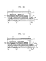
- FIG. 1A is a cross-sectional view illustrating an organic light-emitting apparatus (a cross-sectional view taken along line I-I' of FIG. 1B ) according to an embodiment
- FIG. 1B is a plan view of the organic light-emitting apparatus of FIG. 1A , in which an encapsulation substrate, a second electrode, an organic layer, and an insulating layer are not shown;
- FIG. 2 is a cross-sectional view of a sealing member according to an embodiment
- FIGS. 3A through 3D are cross-sectional views sequentially illustrating a method of manufacturing the organic light-emitting apparatus of FIG. 1A , according to an embodiment
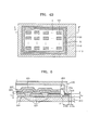
- FIG. 4A is a cross-sectional view illustrating an organic light-emitting apparatus (a cross-sectional view taken along line I-I' of FIG. 4B ) according to another embodiment;
- FIG. 4B is a plan view of the organic light-emitting apparatus of FIG. 4A , in which an encapsulation layer, a second electrode, an organic layer, and an insulating layer are not shown;
- FIG. 5 is a cross-sectional view illustrating an organic light-emitting device according to another embodiment
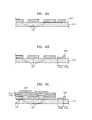
- FIGS. 6A through 6D are cross-sectional views sequentially illustrating a method of manufacturing the organic light-emitting apparatus of FIG. 5 , according to another embodiment.
- FIG. 7 is a cross-sectional view illustrating an organic light-emitting apparatus according to another embodiment.
- FIG. 1A is a cross-sectional view illustrating an organic light-emitting apparatus (a cross-sectional view taken along line I-I' of FIG. 1B ) according to an embodiment.
- FIG. 1B is a plan view of the organic light-emitting apparatus of FIG. 1A , in which an encapsulation substrate 30, a second electrode 27, an organic layer 25, and an insulating layer 23 are not shown.
- the organic light-emitting apparatus includes a device substrate 10, the encapsulation substrate 30, a first electrode 21, the insulating layer 23, the organic layer 25, the second electrode 27, a sealing member 50, and a third electrode 40 including a first portion 40a.
- the first electrode 21, the insulating layer 23, the organic layer 25, and the second electrode 27 may constitute an organic light-emitting device 20.
- the organic light-emitting apparatus includes a space 60 between the device substrate 10 and the encapsulation substrate 30.
- numerical reference numerals recited in the figures have been included below, these are not to be taken to limit the scope of the present invention. They are included just for ease of reference.
- the device substrate 10, in any embodiment of the present, which may preferably be any substrate that is used in conventional organic light-emitting apparatuses, may be a glass substrate or a transparent plastic substrate with excellent mechanical strength, thermal stability, transparency, surface smoothness, ease of handling, and water resistance.
- the device substrate 10 may preferably comprise an inorganic material such as a transparent glass material mainly formed of SiO 2 , or an insulating organic material such as a transparent plastic material.
- the insulating organic material may preferably be selected from the group consisting of, for example, polyethersulphone (PES), polyacrylate (PAR), polyetherimide (PEI), polyethyelenen naphthalate (PEN), polyethyeleneterephthalate (PET), polyphenylene sulfide (PPS), polyallylate, polyimide, polycarbonate (PC), cellulose tri acetate (TAC), and cellulose acetate propionate (CAP), but the present embodiment is not limited thereto.
- PES polyethersulphone
- PAR polyacrylate
- PEI polyetherimide
- PEN polyethyelenen naphthalate
- PET polyethyeleneterephthalate
- PPS polyphenylene sulfide
- polyallylate polyimide
- PC polycarbonate
- TAC cellulose tri acetate
- CAP cellulose acetate propionate
- the device substrate 10 may preferably comprise a transparent material.
- the organic light emitting apparatus of the present invention for example, that disclosed in FIG. 1A
- the device substrate 10 may preferably comprise a non-transparent material. In the latter case, the device substrate 10 may preferably comprise a metal.
- the device substrate 10 may preferably include at least one material selected from the group consisting of carbon, iron, chromium, manganese, nickel, titanium, molybdenum, stainless steel (SUS), an Invar alloy, an Inconel alloy, and a Kovar alloy, but the present embodiment is not limited thereto.
- a buffer layer (not shown) for planarizing the device substrate 10 and preventing penetration of impurities may be formed on a top surface of the device substrate 10.
- the device substrate 10 includes a light-emitting area A and a non-emitting area (see, for example, the area other than the light-emitting area "A" in FIG. 1B ).
- the encapsulation substrate 30 may preferably be disposed to face the device substrate 10.
- the encapsulation substrate 30 may preferably be formed to cover the light-emitting area A.
- the encapsulation substrate 30 may preferably comprise various materials.
- the aforesaid materials of the device substrate 10 are referred to.
- the organic light-emitting device 20 is disposed between the device substrate 10 and the encapsulation substrate 30.
- the organic light-emitting device 20 may preferably include the first electrode 21, the insulating layer 23, and the second electrode 27.
- the first electrode 21 may preferably be an anode (a hole injection electrode), and may preferably be formed by deposition or sputtering using a material having a high work function.
- the first electrode 21 may preferably include at least one material selected from the group consisting of metals and conductive oxides.
- the first electrode 21 may preferably include a metal selected from silver (Ag), magnesium (Mg), aluminum (A1), platinum (Pt), palladium (Pd), gold (Au), nickel (Ni), neodymium (Nd), iridium (Ir), chromium (Cr), and a combination of two or more metals; or a conductive oxide selected from indium tin oxide (ITO), indium zinc oxide (IZO), zinc oxide (ZnO), and indium oxide (In 2 0 3 ).
- the first electrode 21 may preferably comprise a combination (e.g., a mixture or a multi-layer structure) of a metal and a conductive oxide.
- the first electrode 21 may preferably comprise ITO, but the present embodiment is not limited thereto.
- the insulating layer 23 may preferably act as a pixel defining layer.
- the insulating layer 23 may preferably comprise a general insulating material.
- the insulating layer 23 may preferably comprise silicon oxide or silicon nitride, but the present embodiment is not limited thereto.
- the organic layer 25 may preferably include at least one of a hole injection layer (HIL), a hole transport layer (HTL), an emission layer (EML), a hole blocking layer (HBL), an electron transport layer (ETL) and an electron injection layer (EIL). Each layer of the organic layer 25 will be explained later.
- HIL hole injection layer
- HTL hole transport layer
- EML emission layer
- HBL hole blocking layer
- ETL electron transport layer
- EIL electron injection layer
- the second electrode 27 may preferably be a cathode (an electron injection electrode), and may preferably comprise a metal, an alloy, an electrically conductive compound, or a mixture thereof which has a relatively low work function.
- examples of such materials include lithium (Li), magnesium (Mg), aluminum (A1), aluminum-lithium (Al-Li), calcium (Ca), magnesium-indium(Mg-ln), and magnesium-silver (Mg-Ag).
- the second electrode 27 may preferably comprise ITO or IZO to achieve a top-emission light emitting device.
- the organic light-emitting device 20 is disposed between the device substrate 10 and the encapsulation substrate 30 as described above, and the device substrate 10 and the encapsulation substrate 30 may preferably be attached to each other by the sealing member 50 that surrounds the light-emitting area A.
- the sealing member 50 may preferably comprise an adhesive material so as to attach the device substrate 10 to the encapsulation substrate 30. Also, in order to prevent external oxygen and/or moisture from permeating into the space 60 between the encapsulation substrate 30 and the device substrate 10, the sealing member 50 may preferably have moisture and/or oxygen-preventing characteristics.
- the sealing member 50 may preferably include at least one of an adhesive and glass frit.
- the adhesive may preferably include at least one of an organic adhesive, an inorganic adhesive, and an organic/inorganic composite adhesive.
- the adhesive may preferably be a cured product (e.g., a cross-linked product) of an adhesive precursor (e.g., a monomer used to form the adhesive).
- Examples of the organic adhesive may preferably include an acryl-based resin, a methacry-based resin, polyisoprene, a vinyl-based resin, an epoxy-based resin, a urethane-based resin, and a cellulose-based resin.
- Examples of the acryl-based resin may preferably include butylacrylate and ethylhexylacrylate.
- Examples of the methacry-based resin may preferably include propylene glycol methacrylate, and tetrahydrofurfuryl methacrylate.
- Examples of the vinyl-based resin may preferably include vinylacetate and N-vinylpyrrolidone.
- Examples of the epoxy-based resin may preferably include cycloaliphatic epoxide, epoxy acrylate, and vinyl epoxy-based resin.
- Examples of the urethane-based resin may preferably include urethane acrylate.
- Examples of the cellulose-based resin may preferably include cellulosenitrate. However, the present embodiment is not limited thereto.
- Examples of the inorganic adhesive may preferably include titania, silicon oxide, zirconia, and alumina.
- organic/inorganic composite adhesive may preferably include 3-glycidoxypropyltrimethoxysilane or a polymer thereof; epoxy silicate; vinyl silane such as vinyltriethoxysilnae or a polymer thereof; amine silane or a derivative thereof such as 3-aminopropyltriethoxysilnae or a polymer thereof; methacrylate silane such as 3-(trimethoxysilyl)propyl acrylate or a polymer thereof; and aryl silane or a derivative thereof such as penyl silane or a polymer thereof, but the present embodiment is not limited thereto.
- the glass frit may preferably be obtained by performing heat treatment (e.g., melting) on a glass frit precursor.
- the glass frit precursor may preferably be any of various metal oxides and non-metal oxides.
- the heat treatment may preferably be performed on the glass frit precursor by using, for example, a laser beam, but the present embodiment is not limited thereto.
- the sealing member 50 may preferably include at least one of a silicon-based compound represented by Formula I and a cured product of the silicon-based compound:
- Q 1 is a divalent group represented by -C(R 1 )(R 2 )-;
- Q 2 is a divalent group represented by -C(R 3 )(R 4 )-C(R 5 )(R 6 )-C(R 7 )(R 8 )-;
- Q 3 is a divalent group represented by -C(R 9 )(R 10 )-C(R 11 )(R 12 )-;
- Q 4 is a divalent group represented by -C(R) 3 )(R) 4 )-;
- Q 5 is a divalent group represented by -C(R 15 )(R 16 )-;
- R 1 through R 16 are each independently selected from the group consisting of H, -F, -CH 3 , -CH 2 F, -CHF 2 , and -CF 3 ;
- Y 1 is a divalent organic group
- Z 1 is a C 1 -C 30 alkyl group or a C 1 -C 30 alkyl group that is substituted with at least one -F;
- Z 2 is a C 1 -C 30 alkoxy group or a C 1 -C 30 alkoxy group that is substituted with at least one -F;
- a and e are each independently an integer from 1 to 20;
- b, c, and d are each independently an integer from 0 to 200, and a case where b, c, and d are all 0 is excluded;
- f is an integer from 0 to 10;
- g is an integer from 0 to 3.
- Q may preferably be a divalent group represented by -CF 2 -, -CHF-, -CF(CF 3 )-, or -C(CF 3 ) 2 -.
- Q 1 may preferably be -CF 2 -.
- a may preferably be an integer from 1 to 5, for example, 2, 3, or 4, but the present embodiment is not limited thereto. If a is 2 or greater, at least two Q 1 may preferably be the same or different.
- F-[Q 1 ] a -" may preferably be CF 3 CF 2 CF 2 -, but the present embodiment is not limited thereto.
- Q 2 may preferably be a divalent group represented by ⁇ CF 2 CF 2 CF 2 -, -CF(CF 3 )CF 2 CF 2 -, -CF 2 CF 2 CH 2 -, or -CH 2 CF 2 CHF-.
- Q 2 may preferably be -CF 2 CF 2 CF 2 - or -CF 2 CF 2 CH 2 -.
- b may preferably be an integer from 0 to 50, for example, an integer from 0 to 45, 0 to 31, 5 to 25 or 10 to 20, but the present embodiment is not limited thereto. If b is 2 or greater, at least two Q 2 may preferably be the same or different.
- a preferred combination of at least two Q 2 includes ⁇ CF 2 CF 2 CF 2 - and - CF 2 CF 2 CH 2 -.
- b may preferably be 0.
- "-[Q 2 -O] b -" may preferably be -(CF 2 CF 2 CF 2 O) 21 CF 2 CF 2 CH 2 O-, - (CF 2 cF 2 CF 2 O) 30 CF 2 CF 2 CH 2 O-, -(CF 2 CF 2 CF 2 O) 21 -, -(CF 2 CF 2 CF 2 O) 11 CF 2 CF 2 CH 2 O-, or - (CF 2 CF 2 CF z O) 11 -, but the present embodiment is not limited thereto.
- Q 3 may preferably be a divalent group represented by - CF 2 CF 2 -, -CF(CF 3 )CF 2 -, -CF 2 CH 2 -, -CF(CF 3 )CH 2 -, or -CH 2 CHF-.
- c may preferably be an integer from 0 to 20, for example, an integer from 0 to 10, or for example, an integer from 1 to 6, but the present embodiment is not limited thereto. If c is 2 or greater, at least two Q 3 may preferably be the same or different.
- a preferred combination of at least two Q 3 includes -CF(CF 3 )CH 2 - and --CF(CF 3 )CF 2 -.
- c may preferably be 0.
- "-[Q 3 -O] c ,-" may preferably be -CF(CF 3 )CH 2 O-, -[CF(CF 3 )CF 2 O] 3 -, - [CF(CF 3 )CF 2 O] 3 CF(CF 3 )CH 2 O-, -[CF(CF 3 )CF 2 O] 4 CF(CF 3 )CH 2 O-, or - [CF(CF 3 )CF 2 O] 5 CF(CF 3 )CH 2 O-, but the present embodiment is not limited thereto
- Q 4 may preferably be a divalent group represented by -CF 2 -, -CF(CF 3 )-, -CHF-, or -CH(CF 3 )-.
- d may preferably be an integer from 0 to 20, for example, an integer from 0 to 20, 0 to 15, 0 to 10, or 1 to 10, but the present embodiment is not limited thereto. If d is 2 or greater, at least two Q 4 may preferably be the same or different.
- d may preferably be 0.
- "-[Q 4 -0] d -" may preferably be -(CF 2 O) 10 -, but the present embodiment is not limited thereto.
- Q 5 may preferably be a divalent group represented by -CH 2 -, -CF 2 -, -CF(CF 3 )-, -CHF-, or -CH(CF 3 )-.
- e may preferably be an integer from 1 to 20, for example, an integer from 1 to 10, or for example, an integer from 1 to 5, preferably 1 to 3, but the present embodiment is not limited thereto. If e is 2 or greater, at least two Q 5 may preferably be the same or different.
- "-[Q 5 ] e -" may preferably be -CH 2 CH 2 CH 2 -, - CF 2 CF 2 - or -CF(CF 3 )-, but the present embodiment is not limited thereto.
- Y 1 may preferably be a divalent group selected from the group consisting of -CONH-, -Si(R 20 )(R 21 )-, a C 2 -C 20 alkylene group (e.g., an ethylene group, a propylene group, a butylene group, or a pentylene group) and a C 2 -C 20 alkylene group that is substituted with at least one ⁇ F, preferably at least two -F, more preferably at least five ⁇ F, for example between 1 and 20 -F.
- a divalent group selected from the group consisting of -CONH-, -Si(R 20 )(R 21 )-, a C 2 -C 20 alkylene group (e.g., an ethylene group, a propylene group, a butylene group, or a pentylene group) and a C 2 -C 20 alkylene group that is substituted with at least one ⁇ F, preferably at least two
- R 20 and R 21 may preferably be each independently selected from the group consisting of a C 1 -C 10 alkyl group (e.g., a methyl group, an ethyl group, a propyl group, a butyl group, a pentyl group, or a hexyl group), a C 1 -C 10 alkyl group that is substituted with at least one F, a C 1 -C 10 alkoxy group (e.g., a methoxy group, an ethoxy group, a propoxy group, a butoxy group, or a pentoxy group), and a C 1 -C 10 alkoxy group that is substituted with at least one F.
- f may preferably be an integer from 0 to 5
- f may preferably be 0.
- "-[Y 1 ] f -" may preferably be -CONH-CH 2 CH z CH 2 -, -Si(Me) 2 -Si(OMe) 2 -CH 2 CH 2 -, or -CONH-CH 2 CH 2 CH 2 -Si(Me) 2 -Si(OMe) 2 -CH 2 CH 2 -, but the present embodiment is not limited thereto. (In the above, Me is a methyl group.)
- Z 1 may preferably be a C 1 -C 10 alkyl group or a C 1 -C 10 alkyl group that is substituted with at least one -F, preferably at least two ⁇ F, more preferably at least five -F, for example, between 1 and 20 -F.
- Z 1 may preferably be a methyl group, an ethyl group, a propyl group, a butyl group, or a pentyl group.
- Z 2 may preferably be a C 1 -C 10 alkoxy group or a C 1 -C 10 alkoxy group that is substituted with at least one -F, preferably at least two -F, more preferably at least five -F, for example between 1 and 20 -F.
- Z 2 may preferably be a methoxy group, an ethoxy group, a propoxy group, a butoxy group, or a pentoxy group.
- g may preferably be 0, 1, 2, or 3.
- g may preferably be 0.
- Preferred embodiments of Formula 1 are defined by the following:
- the sealing member 50 may preferably include the silicon-based compound.
- the sealing member 50 when the sealing member 50 is formed, according to whether heat, a cross-linking catalyst, or the like is provided, a cured product of the silicon-based compound that is cross-linked may preferably be formed. Accordingly, the sealing member 50 may preferably include a cured product of the silicon-based compound.
- the necessary conditions for curing a compound of Formula 1 may be selected in consideration of the chemical formula of said compound.
- the sealing member 50 may preferably include both the silicon-based compound and the cured product of the silicon-based compound.
- a self-assembly monolayer may preferably be additionally formed in an area of the sealing member 50 contacting the device substrate 10, an area of the sealing member 50 contacting the encapsulation substrate 30, an area of the sealing member 50 contacting the first portion 40a of the third electrode 40, and/or an area of the sealing member 50 contacting a second portion 240b of the third electrode 240 that will be explained later.
- SAM self-assembly monolayer
- the SAM may preferably be formed by a reaction between Z 2 of the silicon-based compound and a hydrophilic group, for example, -OH, which may preferably exist in the device substrate 10, the encapsulation substrate 30, the first portion 40a of the third electrode 40, and/or the second portion 240b of the third electrode 240.
- the SAM may preferably include a moiety represented by Formula 1a:
- Formula 1 For information about the substituents in the moiety represented by Formula 1a, Formula 1 is referred to, In Formula 1a, h is an integer from 0 to 2, and * is a binding site with a surface of an area where the SAM is formed from the silicon-based compound. For example, in Formula 1a, * is a binding site with a surface of the device substrate 10, a surface of the encapsulation substrate 30, a surface of the first portion 40a of the third electrode 40, and/or a surface of the second portion 240b of the third electrode 240.
- Which combination the sealing member 50 includes from at least one of the silicon-based compound represented by Formula 1 and the cured product of the silicon-based compound (and optionally, the SAM formed from the silicon-based compound) may preferably vary according to conditions under which the sealing member 50 is formed.
- the silicon-based compound may preferably provide very low surface energy. Accordingly, since a surface, which is exposed to the outside, of the sealing member 50 including at least one of the silicon-based compound represented by Formula 1 and the cured product of the silicon-based compound (and optionally, the SAM formed from the silicon-based compound) has low surface energy, moisture and/or oxygen may preferably not attach itself to the surface of the sealing member 50. Accordingly, moisture and/or oxygen are prevented from permeating through the sealing member 50.
- the sealing member 50 may preferably have a multi-layer structure including two or more materials.
- the sealing member 50 may preferably include a first sealing member layer 51b, a second sealing member layer 53, and a third sealing member layer 51a which are sequentially stacked from the device substrate 10 (or from the second portion 240b of the third electrode 240 as will be described later).
- Each of the first sealing member layer 51b and the third sealing member layer 51a may preferably include the aforesaid adhesive.
- the second sealing member 53 may preferably include at least one of the silicon-based compound represented by Formula 1 and the cured product of the silicon-based compound (and optionally, the SAM formed from the silicon-based compound).
- the third electrode 40 is disposed on the non-emitting area outside the sealing member 50.
- the third electrode 40 includes the first portion 40a that surrounds the sealing member 50.
- the first electrode 21 and the third electrode 40 are formed of the same material.
- each of the first electrode 21 and the third electrode 40 may preferably comprise ITO, but the present embodiment is not limited thereto.
- a side surface of the sealing member 50 and a side surface of the first portion 40a of the third electrode 40 contact each other. Accordingly, oxygen and/or moisture are substantially prevented from permeating into the space 60, if present, between the encapsulation substrate 30 and the device substrate 10 through the side surface of the sealing member 50, thereby preventing the organic light-emitting device 20 from deteriorating due to the oxygen and/or moisture.
- the third electrode 40 may preferably be a "floating electrode” that is not connected to a power supply source, unlike the first electrode 21 and the second electrode 27.
- a maximum thickness L 1 of the first electrode 21 and a maximum thickness L 2 of the first portion 40a of the third electrode 40 may preferably have a relationship of L 1 ⁇ L 2 .
- the maximum thickness L 2 of the first portion 40a of the third electrode 40 and a maximum thickness L 3 of the sealing member 50 may preferably have a relationship of L 2 ⁇ L 3 .
- the side surface of the sealing member 50 is not exposed to the outside. Accordingly, oxygen and/or moisture are effectively prevented from permeating into the space 60, if present, between the encapsulation substrate 30 and the device substrate 10 through the side surface of the sealing member 50, thereby preventing the organic light-emitting device 20 from deteriorating due to the moisture and/or oxygen.
- the space 60 between the device substrate 10 and the encapsulation substrate 30 may preferably be a vacuum space.
- a moisture-absorbing layer (not shown in FIG. 1A ) may preferably be further included in the space 60 between the device substrate 10 and the encapsulation substrate 30.
- the moisture-absorbing layer may preferably be located on a bottom surface of the encapsulation substrate 30 or an inner side of the sealing member 50.
- the moisture-absorbing layer absorbs oxygen and/or moisture, even though it is a small amount, being present in the space 60 between the device substrate 10 and the encapsulation substrate 30.
- the moisture-absorbing layer may preferably include a metal oxide having an average diameter of 100 nm or less.
- the metal oxide may preferably be alkali metal oxide or alkaline earth metal oxide.
- Examples of the alkali metal oxide may preferably include lithium oxide (Li 2 0), sodium oxide (Na 2 O) and potassium oxide (K 2 0), and examples of the alkaline earth metal oxide may preferably include barium oxide (BaO), calcium oxide (CaO) and magnesium oxide (MgO), but the present embodiment is not limited thereto.
- the moisture-absorbing layer may preferably further, optionally, include a binder and a dispersing agent.
- a filler (not shown in FIG. 1A ) may preferably fill the space 60 between the device substrate 10 and the encapsulation substrate 30. Accordingly, the space 60 between the device substrate 10 and the encapsulation substrate 30 is completely filled by the organic light-emitting device 20 and the filler, and there may preferably no empty space between the device substrate 10 and the encapsulation substrate 30.
- the filler may preferably be a material having a predetermined visible light transmittance so as not to substantially react with a material of the organic light-emitting device 20 and to enable light emitted from the organic light-emitting device 20 to be effectively extracted to the outside.
- the filler may preferably be silicone, an epoxy resin, or the like.
- the filler may preferably include at least one of the silicon-based compound represented by Formula I and the cured product of the silicon-based compound (and optionally, the SAM formed from the silicon-based compound).
- Formula 1 has been described above, and will not be described herein.
- the silicon-based compound Since the silicon-based compound has low surface energy, if the silicon-based compound represented by Formula 1 is used as the filler, moisture and/or oxygen being present between the device substrate 10 and the encapsulation substrate 30, even though it is a small amount, is prevented from reaching the organic light-emitting device 20. Accordingly, the organic light-emitting device 20 is effectively prevented from deteriorating due to the moisture and/or oxygen, thereby making it possible to realize an organic light-emitting apparatus having a long lifetime.
- FIGS. 3A through 3D A method of manufacturing the organic light-emitting apparatus of the present invention, for example the embodiment illustrated in FIGS. 1A and 1B , will now be explained with reference to FIGS. 3A through 3D .
- the device substrate 10 including the light-emitting area and the non-emitting area is prepared.
- the device substrate 10 may preferably include a driving transistor or a switching transistor.
- the first electrode 21 is formed in the light-emitting area of the device substrate 10, and the third electrode 40 including the first portion 40a is formed in the non-emitting area of the device substrate 10.
- the third electrode 40 and the first electrode 21 may preferably be simultaneously formed.
- the first electrode 21 and the third electrode 40 each formed of ITO may preferably be simultaneously formed by forming an ITO layer in the light-emitting area and the non-emitting area of the device substrate 10 and simultaneously patterning the first electrode 21 and the third electrode 40.
- the first electrode 21 and the third electrode 40 each formed of ITO may preferably be simultaneously formed by depositing ITO on the device substrate 10 by using a mask including patterns of the first electrode 21 and the third electrode 40.
- the thickness L 1 of the first electrode 21 and the thickness L 2 of the third electrode 40 may preferably be the same.
- the method since the third electrode 40 is also formed when the first electrode 21 is formed, a separate process of forming the third electrode 40 is not necessary. Accordingly, the method of manufacturing the organic light-emitting apparatus may preferably be performed in an easy and simple manner at low cost.
- the first electrode 21 and the third electrode 40 may preferably be formed by a well-known method (e.g., laser etching, wet etching, or deposition using a mask including a predetermined pattern).
- the insulating layer 23 formed on both ends of the first electrode 21, the organic layer 25, and the second electrode 27 are sequentially formed, thereby forming the organic light-emitting device 20.
- the HIL may preferably be formed by any well-known method such as vacuum deposition, spin-coating, casting, or Langmuir-Blodgett (LB) deposition.
- deposition conditions may preferably vary according to a target compound that is used to form the HIL, and the structure and thermal characteristics of the HIL to be formed.
- the deposition conditions may preferably include a deposition temperature of about 100°C to about 500°C, a degree of vacuum of about 10 -10 to about 10 -3 torr, and a deposition rate of about 0.01 to 100 ⁇ /sec.
- coating conditions may preferably vary according to a target compound that is used to form the HIL, and the structure and thermal characteristics of the HIL to be formed.
- the coating conditions may preferably include a coating speed of about 2000 rpm to 5000 rpm and a heat treatment temperature of about 80°C to 200°C (at which a solvent is removed after coating).
- the HIL may preferably comprise any material that is commonly used to form an HIL.
- the material that may preferably be used to form the HIL include a phthalocyanine compound such as copperphthalocyanine, 4,4',4"-tris (3-methylphenylphenylamino) triphenylamine (m-MTDATA, see the following formula), N,N'-di(1-naphthyl)-N,N'-diphenylbenzidine (NPB), TDATA (see the following formula), 2T-NATA (see the following formula), polyaniline/dodecylbenzenesulfonic acid (Pani/DBSA), poly(3,4-ethylenedioxythiophene)/poly(4-styrenesulfonate) (PEDOT/PSS), polyaniline/camphor sulfonic acid (Pani/CSA), and polyaniline/poly(4-styrenesulfonate (PANT/PSS), but the present embodiment is not limited there
- a thickness of the HIL may preferably be in a range of about 10 to about 10,000 A, for example, about 100 to about 1,000 ⁇ . When the thickness of the HIL is within this range, the HIL may preferably have excellent hole injection properties without an increase in driving voltage.
- the HTL may preferably be formed by a method selected from various well-known methods such as vacuum deposition, spin coating, casting, and Langmuir-Blodgett (LB) deposition.
- deposition conditions and coating conditions may preferably vary according to a target compound and the structure and thermal characteristics of the HTL to be formed, but may preferably be the same or similar to those described with reference to the HIL.
- the HTL may preferably comprise any material that is commonly used to form an HTL.
- the material that may preferably be used to form the HTL include: N-phenylcarbazole; an amine derivative having an aromatic condensation ring such as N,N'-bis(3-methylphenyl)-N,N'-diphenyl-[1,1-biphenyl]-4,4'-diamine (TPD); and a triphenylamine-based material such as 4,4',4"-tris(N-carbazolyl)triphenylamine (TCTA).
- TPD N,N'-bis(3-methylphenyl)-N,N'-diphenyl-[1,1-biphenyl]-4,4'-diamine
- TCTA triphenylamine-based material
- TCTA may preferably not only transport holes but also inhibit excitons from being diffused from the EML.
- a thickness of the HTL may preferably be in a range of about 50 to 1,000 ⁇ , for example, about 100 to about 600 ⁇ . When the thickness of the HTL is within this range, the HTL may preferably have excellent hole-transporting properties without a substantial increase in driving voltage.
- the EML may preferably be formed by any well-known method such as vacuum deposition, spin-coating, casting, or Langmuir-Blodgett (LB) deposition.
- deposition conditions and coating conditions may preferably vary according to a target compound and the structure and thermal characteristics of the EML to be formed, but may preferably be the same or similar to those described with reference to the HIL.
- the EML may preferably include only a single light-emitting material. In some cases, however, the EML may preferably include a host and a dopant.
- Examples of the host may preferably include aluminum tris(8-hydroxyquinoline) (Alq 3 ), 4,4'-N,N'-dicarbazole-biphenyl (CBP), 9,10-di(naphthalene-2-yl)anthracene (ADN), TCTA, 1,3,5-tris(N-phenylbenzimidazole-2-yl)benzene) (TPBI), 3-tert-butyl-9,10-di(naphth-2-yl)anthracene (TBADN), and E3, but the present embodiment is not limited thereto.
- Alq 3 aluminum tris(8-hydroxyquinoline)
- CBP 4,4'-N,N'-dicarbazole-biphenyl
- ADN 9,10-di(naphthalene-2-yl)anthracene
- TCTA 1,3,5-tris(N-phenylbenzimidazole-2-yl)benzene)
- TPBI 1,
- red dopants examples include PtOEP, lr(piq) 3 , and Btp 2 Ir(acac), but the present embodiment is not limited thereto.
- examples of well-known blue dopants include F 2 Irpic, (F 2 ppy) 2 Ir(tmd), Ir(df ppz ) 3 , ter-fluorene, 4,4'-bis[4-(di-p-tolylamino)styryl] biphenyl (DPAVBi), and 2,5,8,11-tetra- tert -butyl perylene (TBP), but the present embodiment is not limited thereto.
- a thickness of the EML may preferably be in a range of about 100 to about 1,000 ⁇ , for example, about 100 to about 600 ⁇ . When the thickness of the EML is within this range, the EML may preferably have excellent light-emitting properties without a substantial increase in driving voltage.
- the HBL which blocks triplet excitons or holes from diffusing into, for example, a cathode, may preferably be further formed on the EML.
- the HBL may preferably be formed by a method selected from various well-known methods such as vacuum deposition, spin coating, casting, and Langmuir-Blodgett (LB) deposition.
- deposition conditions and coating conditions may preferably vary according to a target compound and the structure and thermal characteristics of the HBL to be formed, but may preferably be the same or similar to those described with reference to the HIL.
- the HBL may preferably comprise any well-known hole blocking material.
- hole blocking materials may preferably include an oxadiazole derivative, a triazole derivative, and a phenanthroline derivative.
- a thickness of the HBL may preferably be in a range of about 50 to 1,000 ⁇ , for example, about 100 to about 300 ⁇ . When the thickness of the HBL is within this range, the HBL may preferably have excellent hole blocking characteristics without a substantial increase in driving voltage.
- the ETL may preferably be formed on the EML or the HBL by a method selected from various well-known methods such as vacuum deposition, spin coating, casting, and Langmuir-Blodgett (LB) deposition.
- deposition conditions and coating conditions may preferably vary according to a target compound and the structure and thermal characteristics of the ETL to be formed, but may preferably be the same or similar to those described with reference to the HIL.
- the ETL may preferably comprise any well-known electron transporting material.
- electron transporting materials include tris(8-quinolinolate)aluminum (Alq 3 ), TAZ, 4,7-diphenyl-1,10-phenanthroline (Bphen), BCP, BeBq 2 , and BA1q:
- a thickness of the ETL may preferably be in a range of about 100 to about 1,000 ⁇ , for example, about 200 to about 500 ⁇ . When the thickness of the ETL is within this range, the ETL may preferably have excellent electron transport properties without a substantial increase in driving voltage.
- the EIL may preferably be formed on the ETL.
- the EIL may preferably comprise any well-known electron injection material such as LiF, NaCl, CsF, Li 2 O, or BaO.
- Deposition conditions for forming the EIL may preferably vary according to a compound that is used to form the EIL, but may preferably be similar to those described with reference to the HIL.
- a thickness of the EIL may preferably be in a range of about 1 to about 100 ⁇ , for example, about 5 to about 50 ⁇ . When the thickness of the EIL is within this range, the EIL may preferably have satisfactory electron injection properties without a substantial increase in driving voltage.
- the second electrode 27 is formed on the organic layer 25.
- a width L 12 of the encapsulation substrate 30 may preferably be determined in consideration of considering a width L 11 (see FIGS. 3A and 3B ) of an area of the device substrate 10 inside the third electrode 40.
- the width L 12 of the encapsulation substrate 30 may preferably be determined to be the same as the width L 11 of the area of the device substrate 10 inside the third electrode 40.
- a sealing member forming material 50a for forming the sealing member 50 may preferably be provided between the device substrate 10 and the encapsulation substrate 30 is subjected to a first process D to form the sealing member 50 that is provided in the non-emitting area inside the third electrode 40 to surround the light-emitting area A, and the device substrate 10 and the encapsulation substrate 30 are attached to each other.
- the first process D for forming the sealing member 50 from the sealing member forming material 50a may preferably vary according to the selected sealing member forming material 50a.
- the first process D may preferably be soft baking for removing a solvent included in the sealing member forming material 50a, UV radiation and/or heat treatment for curing the sealing member forming material 50a, or laser beam radiation, which is a kind of heat treatment, for melting the sealing member forming material 50a.
- the providing of the sealing member 50 for attaching the device substrate 10 and the encapsulation substrate 30 to each other may preferably be performed by at least one of i) providing an adhesive precursor between the device substrate 10 and the encapsulation substrate 30 and curing the adhesive precursor (by using, for example, UV radiation or heat treatment), ii) providing a glass frit precursor between the device substrate 10 and the encapsulation substrate 30 and performing heat treatment (for example, laser beam radiation), and iii) providing the silicon-based compound represented by Formula 1 between the device substrate 10 and the encapsulation substrate 30.
- Formula 1 is described above, and will not be described again here.
- the method of manufacturing the organic light-emitting apparatus may preferably further include a) creating a vacuum in the space 60 between the device substrate 10 and the encapsulation substrate 30, b) providing a moisture-absorbing layer to the space 60 between the device substrate 10 and the encapsulation substrate 30, and c) providing a filler to the space 60 between the device substrate 10 and the encapsulation substrate 30.
- the filler is described in more detail above.
- the providing of the filler may preferably be performed, for example, after providing the filler to an inner area C of the encapsulation substrate 30, for example in FIG. 3C , by attaching the device substrate 10 and the encapsulation substrate 30.
- FIG. 4A is a cross-sectional view illustrating an organic light-emitting apparatus (a cross-sectional view taken along line I-I' of FIG. 4B ) according to another embodiment.
- FIG. 4B is a plan view of the organic light-emitting apparatus of FIG. 4A , in which an encapsulation substrate 130, a second electrode 127, an organic layer 125, and an insulating layer 123 are not shown.
- 4A and 4B includes a device substrate 110, the encapsulation substrate 130, a first electrode 121, the insulating layer 123, the organic layer 125, the second electrode 127, a sealing member 150, a third electrode 140 including a first portion 140a, and a first layer 170.
- the first electrode 121, the insulating layer 123, the organic layer 125, and the second electrode 127 may preferably constitute an organic light-emitting device 120.
- the organic light-emitting apparatus may preferably include a space 160 between the device substrate 110 and the encapsulation substrate 130.
- the substrate 10 For information about the device substrate 110, the encapsulation substrate 130, the first electrode 121, the insulating layer 123, the organic layer 125, the second electrode 127, the sealing member 150, the third electrode 140 including the first portion 140a, and the space 160 between the device substrate 110 and the encapsulation substrate 130 of the organic light-emitting apparatus of FIGS. 4A and 4B , the substrate 10, the encapsulation substrate 30, the first electrode 21, the insulating layer 23, the organic layer 25, the second electrode 27, the sealing member 50, the third electrode 40 including the first portion 40a, and the space 60 between the device substrate 10 and the encapsulation substrate 30 the embodiments discussed above, for example in respect of FIGS. 1A and 1B , should be referred to.
- the sealing member 150 and the first portion 140a of the third electrode 140 are spaced apart from each other, and a space between the sealing member 150 and the first portion 140a of the third electrode 140 is filled with the first layer 170.
- the first layer 170 may preferably include at least one of the silicon-based compounds represented by Formula 1 and the cured product of the silicon-based compound (and optionally, the SAM formed from the silicon-based compound).
- Formula I is described above, and will not be described again here.
- the silicon-based compound may preferably provide very low surface energy, the surface energy of a surface, which is exposed to external air, of the first layer 170 is very low. Accordingly, since moisture and/or oxygen is prevented by not only the third electrode 140 but also the first layer 170, the organic light-emitting device 120 of the organic light-emitting apparatus of FIGS. 4A and 4B may preferably be effectively prevented from deteriorating due to the moisture and/or oxygen, thereby extending the lifetime of the organic light-emitting apparatus.
- the organic light-emitting apparatus of FIGS. 4A and 4B may preferably be manufactured by attaching the device substrate 110 and the encapsulation substrate 130 so that the width L 12 (see FIG. 3C ) of the encapsulation substrate 130 is less than the width L 11 (see FIG. 3C ) of the device substrate 110 inside the third electrode 140 and forming the first layer 170 in the space between the sealing member 150 and the first portion 140a of the third electrode 140.
- the first layer 170 may preferably be formed by providing the silicon-based compound (and optionally, a solvent) represented by Formula 1 to the space formed between the sealing member 150 and the first portion 140a of the third electrode 140 by any well-known method, such as inkjet printing or nozzle printing, and performing an additional process such as soft baking, but the present embodiment is not limited thereto.
- FIG. 5 is a cross-sectional view illustrating an organic light-emitting apparatus according to another embodiment of the present invention.
- the organic light-emitting apparatus of FIG. 5 includes a device substrate 210, an encapsulation substrate 230, a first electrode 221, an insulating layer 223, an organic layer 225, a second electrode 227, a sealing member 250, a third electrode 240 including a first portion 240a and a second portion 240b, and a first layer 270.
- the first electrode 221, the insulating layer 223, the organic layer 225, and the second electrode 227 may preferably constitute an organic light-emitting device 220.
- the organic light-emitting apparatus includes a space 260 between the device substrate 210 and the encapsulation substrate 230.
- the encapsulation substrate 230 For information about the device substrate 210, the encapsulation substrate 230, the first electrode 221, the insulating layer 223, the organic layer 225, the second electrode 227, the sealing member 250, the first layer 270, the first portion 240a, the third electrode 240, and the space 260 between the device substrate 210 and the encapsulation substrate 230 of the organic light-emitting apparatus of FIG.
- the device substrate 110, the encapsulation substrate 130, the first electrode 121, the insulating layer 123, the organic layer 125, the second electrode 127, the sealing member 150, the first layer 170, the first portion 140a, the third electrode 140, and the space 160 between the device substrate 110 and the encapsulation substrate 130 of the organic light-emitting apparatus the embodiments discussed above, for example in respect of FIGS 1A and 1B and FIGS. 4A and 4B , should be referred to.. ..
- the third electrode 240 of the organic light-emitting apparatus of FIG. 5 includes the first portion 240a that surrounds the sealing member 250, and further includes the second portion 240b that extends from the first portion 240a of the third electrode 240 toward the sealing member 250.
- the maximum thickness L 2 of the first portion 240a of the third electrode 240 and a maximum thickness L 5 of the second portion 240b of the third electrode 240 may preferably have a relationship of L 2 ⁇ L 5 .
- FIG. 5 A method of manufacturing the organic light-emitting apparatus of the present invention, for example that displayed by FIG. 5 , will be explained with reference to FIGS. 6A through 6D .
- the device substrate 210 is prepared, and then the first electrode 221 and a third layer 241 are simultaneously formed.
- the forming of the first electrode 221 and the third layer 241 may preferably be performed by simultaneously forming the first electrode 221 and the third layer 241 without a separate process of forming the third layer 241, like in the forming of the first electrode 21 and the third electrode 24 of FIG. 3A .
- part of the third layer 241 is patterned and thus the first portion 241a and the second portion 240b of the third layer 241 are formed, thereby forming the third electrode 240.
- the first portion 240a and the second portion 240b may preferably be formed by a general patterning method such as laser etching or wet etching.
- the insulating layer 223, the organic layer 225, and the second electrode 227 are sequentially formed, as explained in detail with reference to FIG. 3B .
- the encapsulation substrate 230 and the device substrate 210 are assembled so that a portion of the encapsulation substrate 230 extending toward the device substrate 210 is located on the second portion 240b of the third electrode 240, the sealing member 250 is provided between the encapsulation substrate 230 and the device substrate 210 (in detail, between the encapsulation substrate 230 and the second portion 240b of the third electrode 240), and the encapsulation substrate 230 and the device substrate 210 are attached, as explained in detail with reference to FIG. 3D .
- the first layer 270 is formed in a space 280 formed between the sealing member 250 and the first portion 240a of the third electrode 240, thereby completely manufacturing the organic light-emitting apparatus of FIG. 5 .
- FIG. 7 is a cross-sectional view illustrating an organic light-emitting apparatus according to another embodiment.
- the organic light-emitting apparatus of FIG. 7 includes a device substrate 310, an encapsulation substrate 330, a first electrode 321, an insulating layer 323. an organic layer 325, a second electrode 327, a sealing member 350, a third electrode 340 including a first portion 340a, and a hole 311.
- the first electrode 321, the insulating layer 323, the organic layer 325, and the second electrode 327 may preferably constitute an organic light-emitting device 320.
- the organic light-emitting apparatus includes a space 360 between the device substrate 310 and the encapsulation substrate 330.
- the device substrate 10 For information about the device substrate 310, the encapsulation substrate 330, the first electrode 321, the insulating layer 323, the organic layer 325, the second electrode 327, the sealing member 350, the first portion 340a, the third electrode 340, and the space 360 between the device substrate 310 and the encapsulation substrate 330 of the organic light-emitting apparatus of FIG. 7 , the device substrate 10, the encapsulation substrate 30, the first electrode 21, the insulating layer 23, the organic layer 25, the second electrode 27, the sealing member 50, the first portion 40a, the third electrode 40 and the space 60 between the device substrate 10 and the encapsulation substrate 30 of the organic light-emitting apparatus of FIGS. 1A and 1B are referred to.
- the device substrate 310 of the organic light-emitting apparatus of FIG. 7 includes the hole 311 corresponding to the sealing member 350. Accordingly, the sealing member 350 is formed in the hole 311. Accordingly, since the sealing member 350 may preferably be prevented from being exposed to external air, oxygen and/or moisture permeation through a side surface of the sealing member 350 may preferably be effectively prevented.
- the organic light-emitting apparatus of FIG. 7 may preferably be manufactured by preparing the device substrate 310 in which the hole 311 is already formed.
- a side surface of the sealing member 250 and a side surface of the first portion 240a of the third electrode 240 of the organic light-emitting apparatus of FIG. 5 may preferably contact each other, and the device substrate 10 of the organic light-emitting apparatus of FIG. 1 may preferably further include a hole corresponding to the sealing member 50.
- the organic light-emitting apparatus have a long lifetime because it substantially prevents moisture and/or oxygen permeation.
Landscapes
- Chemical & Material Sciences (AREA)
- Physics & Mathematics (AREA)
- Engineering & Computer Science (AREA)
- Materials Engineering (AREA)
- Spectroscopy & Molecular Physics (AREA)
- Optics & Photonics (AREA)
- Crystallography & Structural Chemistry (AREA)
- Inorganic Chemistry (AREA)
- Electroluminescent Light Sources (AREA)
- Heating, Cooling, Or Curing Plastics Or The Like In General (AREA)
Abstract
Description
- This application claims the benefit of Korean Patent Application No.
10-2010-0066997, filed on July 12, 2010 - An organic light-emitting apparatus and a method of manufacturing the same are provided.
- Organic light-emitting devices, which are self-emitting devices, have advantages such as a wide viewing angle, excellent contrast, quick response, high brightness, and excellent driving voltage characteristics, and may provide multicolor images.
- In general, an organic light-emitting device may include an anode, a cathode, and an organic layer disposed between the anode and the cathode. The organic layer may include a hole transport layer (HTL), an emission layer (EML), an electron transport layer (ETL), and a cathode. When a voltage is applied between the anode and the cathode, holes injected from the anode move to the EML via the HTL, and electrons injected from the cathode move to the EML via the ETL. Carriers such as the holes and electrons recombine in the EML to generate excitons. When the excitons drop from an excited state to a ground state, light is emitted. An organic light-emitting apparatus including the organic light-emitting device may further include a driving transistor or a switching transistor.
- Since the organic light-emitting device may deteriorate due to oxygen and/or moisture, a sealing unit for effectively sealing the organic light-emitting device is required in order to realize a high quality organic light-emitting apparatus.
- An organic light-emitting apparatus having a structure for preventing oxygen and/or moisture permeation is provided.
- A method of manufacturing the organic light-emitting apparatus is also provided.
- According to an aspect of the present embodiments, there is provided an organic light-emitting apparatus including: a device substrate including a light-emitting area and a non-emitting area; an encapsulation substrate covering the light-emitting area; a first electrode formed on the light-emitting area and disposed between the device substrate and the encapsulation substrate; an organic layer disposed between the encapsulation substrate and the first electrode; a second electrode disposed between the organic layer and the encapsulation substrate; a sealing member surrounding the light-emitting area; and a third electrode disposed on the non-emitting area outside the sealing member, including a first portion surrounding the sealing member, and comprising a same material as that of the first electrode.
- Each of the first electrode and the third electrode may preferably include at least one material selected from the group consisting of metals and conductive oxides.
- Each of the first electrode and the third electrode may preferably comprise indium tin oxide (ITO).
- The sealing member may preferably include at least one of an adhesive and glass frit.
- The sealing member may preferably include at least one of a silicon-based compound represented by Formula 1 and a cured product of the silicon-based compound:
<Formula 1> F-[Q1]a-O-[Q2-O]b-[-Q3-O]c-[Q4-O]d-[Q5]e-[Y1]f-Si(Z1)g(Z2)3-g.
- Where Q1 is a divalent group represented by -C(R1)(R2)-; Q2 is a divalent group represented by -C(R3)(R4)-C(R5)(R6)-C(R7)(R8)-; Q3 is a divalent group represented by -C(R9)(R10)-C(R11)(R12)-; Q4 s a divalent group represented by -C(R13)(R14)-; Q5 is a divalent group represented by -C(R15)(R16)-; R1 through R16 are each independently selected from the group consisting of H, -F, -CH3, -CH2F, -CHF2, and -CF3; Y1 is a divalent organic group; Z1 is a C1-C30 alkyl group or a C1-C30 alkyl group that is substituted with at least one ―F; Z2 is a C1-C30 alkoxy group or a C1―C30 alkoxy group that is substituted with at least one―F; a and e are each independently an integer from 1 to 20; b, c, and d are each independently an integer from 0 to 200, and a case where b, c, and d are all 0 is excluded; f is an integer from 0 to 10; and g is an integer from 0 to 3.
- The sealing member may preferably sequentially include a first sealing member layer, a second sealing member layer, and a third sealing member layer, each of the first sealing member layer and the third sealing member layer may include an adhesive, and the second sealing member layer may include at least one of the silicon-based compound represented by Formula 1 and the cured product of the silicon-based compound;
A side surface of the sealing member and a side surface of the first portion of the third electrode may preferably contact each other. - When a maximum thickness of the first electrode is L1 and a maximum thickness of the first portion of the third electrode is L2, preferably L1=L2.
- When a maximum thickness of the first portion of the third electrode is L2 and a maximum thickness of the sealing member is L3, preferably L2≥L3.
- Preferably there may be a space between the device substrate and the encapsulation substrate, this preferably may be a vacuum space.
- The organic light-emitting apparatus may preferably further include a moisture-absorbing layer disposed in a space, if present, between the device substrate and the encapsulation substrate.
- A filler may preferably fill a space, if present, between the device substrate and the encapsulation substrate
- The filler may preferably include at least one of the silicon-based compound represented by Formula 1 and the cured product of the silicon-based compound.
- Preferably the sealing member and the first portion of the third electrode may be spaced apart from each other, a space between the sealing member and the first portion of the third electrode may be filled with a first layer, and the first layer may include at least one of the silicon-based compound represented by Formula 1 and the cured product of the silicon-based compound.
- When a maximum thickness of the first portion of the sealing member is L3 and a maximum thickness of the first layer is L4, preferably L3≤L4,
- Preferably the third electrode may have a second portion extending from the first portion of the third electrode toward the sealing member, and the second portion of the third electrode may be located between the sealing member and the device substrate.
- When a maximum thickness of the third electrode is L2 and a maximum thickness of the second portion of the third electrode is L5, preferably L2≥L5.
- The device substrate may preferably include a hole corresponding to the sealing member, and the sealing member may be disposed in the hole.
- According to another aspect of the present embodiments, there is provided a method of manufacturing an organic light-emitting apparatus, the method including: preparing a device substrate including a light-emitting area and a non-emitting area; forming a first electrode in the light-emitting area, and forming a third electrode including a first portion and formed of the same material as that of the first electrode in the non-emitting area; forming an organic layer on the first electrode; forming a second electrode on the organic layer, and attaching the device substrate and an encapsulation substrate to each other by assembling the encapsulation substrate with the device substrate so that the encapsulation substrate covers the light-emitting area, and providing a sealing member to the non-emitting area inside the third electrode to surround the light-emitting area.
- Each of the first electrode and the third electrode may preferably include at least one material selected from the group consisting of metals and conductive oxides.
- Each of the first electrode and the third electrode may preferably comprise ITO.
- Preferably the providing of the sealing member of the attaching of the device substrate and the encapsulation substrate to each other may include at least one of: providing an adhesive precursor between the device substrate and the encapsulation substrate and curing the adhesive precursor, providing a glass frit precursor between the device substrate and the encapsulation substrate and performing heat treatment, and providing the silicon-based compound represented by Formula 1 between the device substrate and the encapsulation substrate.
- Preferably the method may further include at least one of creating a vacuum in a space between the device substrate and the encapsulation substrate, providing a moisture-absorbing layer to the space between the device substrate and the encapsulation substrate, and providing a filler to the space between the device substrate and the encapsulation substrate.
- Preferably the method may further include, after the attaching of the device substrate and the encapsulation substrate to each other, providing a first layer including at least one of the silicon-based compound represented by Formula 1 and a cured product of the silicon-based compound to a space between the sealing member and the first portion of the third electrode.
- Preferably the forming of the first electrode and the third electrode may further include additionally forming a second portion extending from the first portion of the third electrode toward the sealing member.
- Preferably the providing of the device substrate including the light-emitting area and the non-emitting area may further include forming a hole corresponding to the sealing member in the non-emitting area of the device substrate.
- The above and other features and advantages of the present embodiments will become more apparent by describing in detail example embodiments thereof with reference to the attached drawings in which:
-
FIG. 1A is a cross-sectional view illustrating an organic light-emitting apparatus (a cross-sectional view taken along line I-I' ofFIG. 1B ) according to an embodiment; -
FIG. 1B is a plan view of the organic light-emitting apparatus ofFIG. 1A , in which an encapsulation substrate, a second electrode, an organic layer, and an insulating layer are not shown; -
FIG. 2 is a cross-sectional view of a sealing member according to an embodiment; -
FIGS. 3A through 3D are cross-sectional views sequentially illustrating a method of manufacturing the organic light-emitting apparatus ofFIG. 1A , according to an embodiment; -
FIG. 4A is a cross-sectional view illustrating an organic light-emitting apparatus (a cross-sectional view taken along line I-I' ofFIG. 4B ) according to another embodiment; -
FIG. 4B is a plan view of the organic light-emitting apparatus ofFIG. 4A , in which an encapsulation layer, a second electrode, an organic layer, and an insulating layer are not shown; -
FIG. 5 is a cross-sectional view illustrating an organic light-emitting device according to another embodiment; -
FIGS. 6A through 6D are cross-sectional views sequentially illustrating a method of manufacturing the organic light-emitting apparatus ofFIG. 5 , according to another embodiment; and -
FIG. 7 is a cross-sectional view illustrating an organic light-emitting apparatus according to another embodiment. - The present embodiments will now be described more fully with reference to the accompanying drawings, in which example embodiments are shown.
-
FIG. 1A is a cross-sectional view illustrating an organic light-emitting apparatus (a cross-sectional view taken along line I-I' ofFIG. 1B ) according to an embodiment.FIG. 1B is a plan view of the organic light-emitting apparatus ofFIG. 1A , in which anencapsulation substrate 30, asecond electrode 27, anorganic layer 25, and an insulatinglayer 23 are not shown. - Referring to
FIGS. 1A and 1B , the organic light-emitting apparatus includes adevice substrate 10, theencapsulation substrate 30, afirst electrode 21, the insulatinglayer 23, theorganic layer 25, thesecond electrode 27, a sealingmember 50, and athird electrode 40 including afirst portion 40a. Thefirst electrode 21, the insulatinglayer 23, theorganic layer 25, and thesecond electrode 27 may constitute an organic light-emittingdevice 20. Meanwhile, the organic light-emitting apparatus includes aspace 60 between thedevice substrate 10 and theencapsulation substrate 30. For ease of reference, numerical reference numerals recited in the figures have been included below, these are not to be taken to limit the scope of the present invention. They are included just for ease of reference. - The
device substrate 10, in any embodiment of the present, which may preferably be any substrate that is used in conventional organic light-emitting apparatuses, may be a glass substrate or a transparent plastic substrate with excellent mechanical strength, thermal stability, transparency, surface smoothness, ease of handling, and water resistance. For example, thedevice substrate 10 may preferably comprise an inorganic material such as a transparent glass material mainly formed of SiO2, or an insulating organic material such as a transparent plastic material. The insulating organic material may preferably be selected from the group consisting of, for example, polyethersulphone (PES), polyacrylate (PAR), polyetherimide (PEI), polyethyelenen naphthalate (PEN), polyethyeleneterephthalate (PET), polyphenylene sulfide (PPS), polyallylate, polyimide, polycarbonate (PC), cellulose tri acetate (TAC), and cellulose acetate propionate (CAP), but the present embodiment is not limited thereto. - If the organic light emitting apparatus of the present invention, for example, that disclosed in
FIG. 1A , is a bottom emission apparatus in which light is emitted from the organic light-emittingdevice 20 toward thedevice substrate 10, thedevice substrate 10 may preferably comprise a transparent material. However, if the organic light emitting apparatus of the present invention, for example, that disclosed inFIG. 1A , is a top emission apparatus in which light is emitted from the organic light-emittingdevice 20 in a direction opposite to thedevice substrate 10, thedevice substrate 10 may preferably comprise a non-transparent material. In the latter case, thedevice substrate 10 may preferably comprise a metal. If thedevice substrate 10 comprises a metal, thedevice substrate 10 may preferably include at least one material selected from the group consisting of carbon, iron, chromium, manganese, nickel, titanium, molybdenum, stainless steel (SUS), an Invar alloy, an Inconel alloy, and a Kovar alloy, but the present embodiment is not limited thereto. - In an embodiment of the present invention, although not shown in the embodiment disclosed in
FIG. 1A , a buffer layer (not shown) for planarizing thedevice substrate 10 and preventing penetration of impurities may be formed on a top surface of thedevice substrate 10. - The
device substrate 10 includes a light-emitting area A and a non-emitting area (see, for example, the area other than the light-emitting area "A" inFIG. 1B ). - The
encapsulation substrate 30 may preferably be disposed to face thedevice substrate 10. Theencapsulation substrate 30 may preferably be formed to cover the light-emitting area A. - The
encapsulation substrate 30 may preferably comprise various materials. For information about preferred materials of theencapsulation substrate 30, the aforesaid materials of thedevice substrate 10 are referred to. - The organic light-emitting
device 20 is disposed between thedevice substrate 10 and theencapsulation substrate 30. The organic light-emittingdevice 20 may preferably include thefirst electrode 21, the insulatinglayer 23, and thesecond electrode 27. - The
first electrode 21 may preferably be an anode (a hole injection electrode), and may preferably be formed by deposition or sputtering using a material having a high work function. Thefirst electrode 21 may preferably include at least one material selected from the group consisting of metals and conductive oxides. For example, thefirst electrode 21 may preferably include a metal selected from silver (Ag), magnesium (Mg), aluminum (A1), platinum (Pt), palladium (Pd), gold (Au), nickel (Ni), neodymium (Nd), iridium (Ir), chromium (Cr), and a combination of two or more metals; or a conductive oxide selected from indium tin oxide (ITO), indium zinc oxide (IZO), zinc oxide (ZnO), and indium oxide (In203). Alternatively, thefirst electrode 21 may preferably comprise a combination (e.g., a mixture or a multi-layer structure) of a metal and a conductive oxide. For example, thefirst electrode 21 may preferably comprise ITO, but the present embodiment is not limited thereto. - The insulating
layer 23 may preferably act as a pixel defining layer. The insulatinglayer 23 may preferably comprise a general insulating material. For example, the insulatinglayer 23 may preferably comprise silicon oxide or silicon nitride, but the present embodiment is not limited thereto. - The
organic layer 25 may preferably include at least one of a hole injection layer (HIL), a hole transport layer (HTL), an emission layer (EML), a hole blocking layer (HBL), an electron transport layer (ETL) and an electron injection layer (EIL). Each layer of theorganic layer 25 will be explained later. - The
second electrode 27 may preferably be a cathode (an electron injection electrode), and may preferably comprise a metal, an alloy, an electrically conductive compound, or a mixture thereof which has a relatively low work function. Examples of such materials include lithium (Li), magnesium (Mg), aluminum (A1), aluminum-lithium (Al-Li), calcium (Ca), magnesium-indium(Mg-ln), and magnesium-silver (Mg-Ag). Alternatively, thesecond electrode 27 may preferably comprise ITO or IZO to achieve a top-emission light emitting device. - The organic light-emitting
device 20 is disposed between thedevice substrate 10 and theencapsulation substrate 30 as described above, and thedevice substrate 10 and theencapsulation substrate 30 may preferably be attached to each other by the sealingmember 50 that surrounds the light-emitting area A. The sealingmember 50 may preferably comprise an adhesive material so as to attach thedevice substrate 10 to theencapsulation substrate 30. Also, in order to prevent external oxygen and/or moisture from permeating into thespace 60 between theencapsulation substrate 30 and thedevice substrate 10, the sealingmember 50 may preferably have moisture and/or oxygen-preventing characteristics. - The sealing
member 50 may preferably include at least one of an adhesive and glass frit. - The adhesive may preferably include at least one of an organic adhesive, an inorganic adhesive, and an organic/inorganic composite adhesive. The adhesive may preferably be a cured product (e.g., a cross-linked product) of an adhesive precursor (e.g., a monomer used to form the adhesive).
- Examples of the organic adhesive may preferably include an acryl-based resin, a methacry-based resin, polyisoprene, a vinyl-based resin, an epoxy-based resin, a urethane-based resin, and a cellulose-based resin.
- Examples of the acryl-based resin may preferably include butylacrylate and ethylhexylacrylate. Examples of the methacry-based resin may preferably include propylene glycol methacrylate, and tetrahydrofurfuryl methacrylate. Examples of the vinyl-based resin may preferably include vinylacetate and N-vinylpyrrolidone. Examples of the epoxy-based resin may preferably include cycloaliphatic epoxide, epoxy acrylate, and vinyl epoxy-based resin. Examples of the urethane-based resin may preferably include urethane acrylate. Examples of the cellulose-based resin may preferably include cellulosenitrate. However, the present embodiment is not limited thereto.
- Examples of the inorganic adhesive may preferably include titania, silicon oxide, zirconia, and alumina.
- Examples of the organic/inorganic composite adhesive may preferably include 3-glycidoxypropyltrimethoxysilane or a polymer thereof; epoxy silicate; vinyl silane such as vinyltriethoxysilnae or a polymer thereof; amine silane or a derivative thereof such as 3-aminopropyltriethoxysilnae or a polymer thereof; methacrylate silane such as 3-(trimethoxysilyl)propyl acrylate or a polymer thereof; and aryl silane or a derivative thereof such as penyl silane or a polymer thereof, but the present embodiment is not limited thereto.
- The glass frit may preferably be obtained by performing heat treatment (e.g., melting) on a glass frit precursor. The glass frit precursor may preferably be any of various metal oxides and non-metal oxides. The heat treatment may preferably be performed on the glass frit precursor by using, for example, a laser beam, but the present embodiment is not limited thereto.
- In any embodiment of the present invention , the sealing
member 50 may preferably include at least one of a silicon-based compound represented by Formula I and a cured product of the silicon-based compound: -
F-[Q1]a-O-[Q2-O]b-[Q3-O]c-[Q4-O]d-[Q5]e-[Y1]fSi(Z1)g(Z2)3-g <Formula 1>
- where Q1 is a divalent group represented by -C(R1)(R2)-;
- Q2 is a divalent group represented by -C(R3)(R4)-C(R5)(R6)-C(R7)(R8)-;
- Q3 is a divalent group represented by -C(R9)(R10)-C(R11)(R12)-;
- Q4 is a divalent group represented by -C(R)3)(R)4)-;
- Q5 is a divalent group represented by -C(R15)(R16)-;
- R1 through R16 are each independently selected from the group consisting of H, -F, -CH3, -CH2F, -CHF2, and -CF3;
- Y1 is a divalent organic group;
- Z1 is a C1-C30 alkyl group or a C1-C30 alkyl group that is substituted with at least one -F;
- Z2 is a C1-C30 alkoxy group or a C1-C30 alkoxy group that is substituted with at least one -F;
- a and e are each independently an integer from 1 to 20;
- b, c, and d are each independently an integer from 0 to 200, and a case where b, c, and d are all 0 is excluded;
- f is an integer from 0 to 10; and
- g is an integer from 0 to 3.
- In Formula 1, Q, may preferably be a divalent group represented by -CF2-, -CHF-, -CF(CF3)-, or -C(CF3)2-. For example, Q1 may preferably be -CF2-. a may preferably be an integer from 1 to 5, for example, 2, 3, or 4, but the present embodiment is not limited thereto. If a is 2 or greater, at least two Q1 may preferably be the same or different.
- For example, in Formula 1, "F-[Q1]a-" may preferably be CF3CF2CF2-, but the present embodiment is not limited thereto.
- In Formula 1, Q2 may preferably be a divalent group represented by ― CF2CF2CF2-, -CF(CF3)CF2CF2-, -CF2CF2CH2-, or -CH2CF2CHF-. For example, Q2 may preferably be -CF2CF2CF2- or -CF2CF2CH2-. b may preferably be an integer from 0 to 50, for example, an integer from 0 to 45, 0 to 31, 5 to 25 or 10 to 20, but the present embodiment is not limited thereto. If b is 2 or greater, at least two Q2 may preferably be the same or different. A preferred combination of at least two Q2 includes ―CF2CF2CF2- and - CF2CF2CH2-.
- For example, in Formula 1, b may preferably be 0. Alternatively, in Formula 1, "-[Q2-O]b-" may preferably be -(CF2CF2CF2O)21CF2CF2CH2O-, - (CF2cF2CF2O)30CF2CF2CH2O-, -(CF2CF2CF2O)21-, -(CF2CF2CF2O)11CF2CF2CH2O-, or - (CF2CF2CFzO)11-, but the present embodiment is not limited thereto.
- In Formula 1, Q3 may preferably be a divalent group represented by - CF2CF2-, -CF(CF3)CF2-, -CF2CH2-, -CF(CF3)CH2-, or -CH2CHF-. c may preferably be an integer from 0 to 20, for example, an integer from 0 to 10, or for example, an integer from 1 to 6, but the present embodiment is not limited thereto. If c is 2 or greater, at least two Q3 may preferably be the same or different. A preferred combination of at least two Q3 includes -CF(CF3)CH2- and --CF(CF3)CF2-.
- For example, in Formula, c may preferably be 0. Alternatively, in Formula 1, "-[Q3-O]c,-" may preferably be -CF(CF3)CH2O-, -[CF(CF3)CF2O]3-, - [CF(CF3)CF2O]3CF(CF3)CH2O-, -[CF(CF3)CF2O]4CF(CF3)CH2O-, or - [CF(CF3)CF2O]5CF(CF3)CH2O-, but the present embodiment is not limited thereto
- In Formula 1, Q4 may preferably be a divalent group represented by -CF2-, -CF(CF3)-, -CHF-, or -CH(CF3)-. d may preferably be an integer from 0 to 20, for example, an integer from 0 to 20, 0 to 15, 0 to 10, or 1 to 10, but the present embodiment is not limited thereto. If d is 2 or greater, at least two Q4 may preferably be the same or different.
- For example, in Formula I, d may preferably be 0. Alternatively, in Formula 1, "-[Q4-0]d-" may preferably be -(CF2O)10-, but the present embodiment is not limited thereto.
- In Formula 1, Q5 may preferably be a divalent group represented by -CH2-, -CF2-, -CF(CF3)-, -CHF-, or -CH(CF3)-. e may preferably be an integer from 1 to 20, for example, an integer from 1 to 10, or for example, an integer from 1 to 5, preferably 1 to 3, but the present embodiment is not limited thereto. If e is 2 or greater, at least two Q5 may preferably be the same or different.
- For example, in Formula 1, "-[Q5]e-" may preferably be -CH2CH2CH2-, - CF2CF2- or -CF(CF3)-, but the present embodiment is not limited thereto.
- In Formula 1, Y1 may preferably be a divalent group selected from the group consisting of -CONH-, -Si(R20)(R21)-, a C2-C20 alkylene group (e.g., an ethylene group, a propylene group, a butylene group, or a pentylene group) and a C2-C20 alkylene group that is substituted with at least one ―F, preferably at least two -F, more preferably at least five ―F, for example between 1 and 20 -F. Here, R20 and R21 may preferably be each independently selected from the group consisting of a C1-C10 alkyl group (e.g., a methyl group, an ethyl group, a propyl group, a butyl group, a pentyl group, or a hexyl group), a C1-C10 alkyl group that is substituted with at least one F, a C1-C10 alkoxy group (e.g., a methoxy group, an ethoxy group, a propoxy group, a butoxy group, or a pentoxy group), and a C1-C10 alkoxy group that is substituted with at least one F. f may preferably be an integer from 0 to 5,
- In Formula 1, f may preferably be 0. Alternatively, in Formula 1, "-[Y1]f-" may preferably be -CONH-CH2CHzCH2-, -Si(Me)2-Si(OMe)2-CH2CH2-, or -CONH-CH2CH2CH2-Si(Me)2-Si(OMe)2-CH2CH2-, but the present embodiment is not limited thereto. (In the above, Me is a methyl group.)
- In Formula 1, Z1 may preferably be a C1-C10 alkyl group or a C1-C10 alkyl group that is substituted with at least one -F, preferably at least two ―F, more preferably at least five -F, for example, between 1 and 20 -F. For example, Z1 may preferably be a methyl group, an ethyl group, a propyl group, a butyl group, or a pentyl group.
- In Formula 1, Z2 may preferably be a C1-C10 alkoxy group or a C1-C10 alkoxy group that is substituted with at least one -F, preferably at least two -F, more preferably at least five -F, for example between 1 and 20 -F. For example, Z2 may preferably be a methoxy group, an ethoxy group, a propoxy group, a butoxy group, or a pentoxy group.
- In Formula 1, g may preferably be 0, 1, 2, or 3. For example, g may preferably be 0. Preferred embodiments of Formula 1 are defined by the following:
- Q1, is a divalent group represented by -CF2-, -CHF-, -CF(CF3)-, or -C(CF3)2-;
- a is 2, 3, or 4;
- Q2 is a divalent group represented by -CF2CF2CF2 or -CF2CF2CH2-;
- b is an integer from 0 to 31;
- Q3 is a divalent group represented by -CF2CF2-, -CF(CF3)CF2-, -CF2CH2-, - CF(CF3)CH2-, or -CH2CHF-;
- c is an integer from 0 to 10;
- Q4 is a divalent group represented by -CF2-, -CF(CF3)-, -CHF-, or -CH(CF3)-;
- d is an integer from 0 to 10;
- Q5 is a divalent group represented by -CH2-, -CF2-, -CF(CF3)-, -CHF-, or -CH(CF3)-;
- e is an integer from 0 to 10;
- -[Y1]f- is -CONH-CH2CH2CH2-, -Si(Me)2-Si(OMe)2-CH2CH2-, or -CONH-CH2CH2CH2-Si(Me)2-Si(OMe)2-CH2CH2-;
- Z1 may preferably be a methyl group, an ethyl group, a propyl group, a butyl group, or a pentyl group;
- Z2 may preferably be a methoxy group, an ethoxy group, a propoxy group, a butoxy group, or a pentoxy group; and
- g is 0 or 1.
- The sealing
member 50 may preferably include the silicon-based compound. - Meanwhile, when the sealing
member 50 is formed, according to whether heat, a cross-linking catalyst, or the like is provided, a cured product of the silicon-based compound that is cross-linked may preferably be formed. Accordingly, the sealingmember 50 may preferably include a cured product of the silicon-based compound. The necessary conditions for curing a compound of Formula 1 may be selected in consideration of the chemical formula of said compound. - Alternatively, the sealing
member 50 may preferably include both the silicon-based compound and the cured product of the silicon-based compound. - Meanwhile, according to conditions under which the sealing
member 50 is formed, a self-assembly monolayer (SAM) may preferably be additionally formed in an area of the sealingmember 50 contacting thedevice substrate 10, an area of the sealingmember 50 contacting theencapsulation substrate 30, an area of the sealingmember 50 contacting thefirst portion 40a of thethird electrode 40, and/or an area of the sealingmember 50 contacting asecond portion 240b of thethird electrode 240 that will be explained later. The SAM may preferably be formed by a reaction between Z2 of the silicon-based compound and a hydrophilic group, for example, -OH, which may preferably exist in thedevice substrate 10, theencapsulation substrate 30, thefirst portion 40a of thethird electrode 40, and/or thesecond portion 240b of thethird electrode 240. The SAM may preferably include a moiety represented by Formula 1a: -
F-[Q1]a-O-[Q2-O]b-[Q3-O]c,-[Q4-O]d-[Q5]e-[Y1]f-Si(Z1)h(Z2)2-h-*. <Formula 1a>
- For information about the substituents in the moiety represented by Formula 1a, Formula 1 is referred to, In Formula 1a, h is an integer from 0 to 2, and * is a binding site with a surface of an area where the SAM is formed from the silicon-based compound. For example, in Formula 1a, * is a binding site with a surface of the
device substrate 10, a surface of theencapsulation substrate 30, a surface of thefirst portion 40a of thethird electrode 40, and/or a surface of thesecond portion 240b of thethird electrode 240. - Which combination the sealing
member 50 includes from at least one of the silicon-based compound represented by Formula 1 and the cured product of the silicon-based compound (and optionally, the SAM formed from the silicon-based compound) may preferably vary according to conditions under which the sealingmember 50 is formed. - The silicon-based compound may preferably provide very low surface energy. Accordingly, since a surface, which is exposed to the outside, of the sealing
member 50 including at least one of the silicon-based compound represented by Formula 1 and the cured product of the silicon-based compound (and optionally, the SAM formed from the silicon-based compound) has low surface energy, moisture and/or oxygen may preferably not attach itself to the surface of the sealingmember 50. Accordingly, moisture and/or oxygen are prevented from permeating through the sealingmember 50. - The sealing
member 50 may preferably have a multi-layer structure including two or more materials. - Preferably, for example, as shown in
FIG. 2 , the sealingmember 50 may preferably include a firstsealing member layer 51b, a secondsealing member layer 53, and a thirdsealing member layer 51a which are sequentially stacked from the device substrate 10 (or from thesecond portion 240b of thethird electrode 240 as will be described later). Each of the firstsealing member layer 51b and the thirdsealing member layer 51a may preferably include the aforesaid adhesive. Thesecond sealing member 53 may preferably include at least one of the silicon-based compound represented by Formula 1 and the cured product of the silicon-based compound (and optionally, the SAM formed from the silicon-based compound). - The
third electrode 40 is disposed on the non-emitting area outside the sealingmember 50. Preferably, for example as shown inFIG. 1A , thethird electrode 40 includes thefirst portion 40a that surrounds the sealingmember 50. Thefirst electrode 21 and thethird electrode 40 are formed of the same material. For example, each of thefirst electrode 21 and thethird electrode 40 may preferably comprise ITO, but the present embodiment is not limited thereto. - A side surface of the sealing
member 50 and a side surface of thefirst portion 40a of thethird electrode 40 contact each other. Accordingly, oxygen and/or moisture are substantially prevented from permeating into thespace 60, if present, between theencapsulation substrate 30 and thedevice substrate 10 through the side surface of the sealingmember 50, thereby preventing the organic light-emittingdevice 20 from deteriorating due to the oxygen and/or moisture. - The
third electrode 40 may preferably be a "floating electrode" that is not connected to a power supply source, unlike thefirst electrode 21 and thesecond electrode 27. - A maximum thickness L1 of the
first electrode 21 and a maximum thickness L2 of thefirst portion 40a of thethird electrode 40 may preferably have a relationship of L1 ‗L2. - Meanwhile, the maximum thickness L2 of the
first portion 40a of thethird electrode 40 and a maximum thickness L3 of the sealingmember 50 may preferably have a relationship of L2≥L3. Here, since a portion of thefirst portion 40a of thethird electrode 40 contacting with the sealingmember 50 has the maximum thickness L2, the side surface of the sealingmember 50 is not exposed to the outside. Accordingly, oxygen and/or moisture are effectively prevented from permeating into thespace 60, if present, between theencapsulation substrate 30 and thedevice substrate 10 through the side surface of the sealingmember 50, thereby preventing the organic light-emittingdevice 20 from deteriorating due to the moisture and/or oxygen. - If present, the
space 60 between thedevice substrate 10 and theencapsulation substrate 30 may preferably be a vacuum space. - Alternatively, a moisture-absorbing layer (not shown in
FIG. 1A ) may preferably be further included in thespace 60 between thedevice substrate 10 and theencapsulation substrate 30. - The moisture-absorbing layer may preferably be located on a bottom surface of the
encapsulation substrate 30 or an inner side of the sealingmember 50. - The moisture-absorbing layer absorbs oxygen and/or moisture, even though it is a small amount, being present in the
space 60 between thedevice substrate 10 and theencapsulation substrate 30. To this end, the moisture-absorbing layer may preferably include a metal oxide having an average diameter of 100 nm or less. The metal oxide may preferably be alkali metal oxide or alkaline earth metal oxide. Examples of the alkali metal oxide may preferably include lithium oxide (Li20), sodium oxide (Na2O) and potassium oxide (K20), and examples of the alkaline earth metal oxide may preferably include barium oxide (BaO), calcium oxide (CaO) and magnesium oxide (MgO), but the present embodiment is not limited thereto. - The moisture-absorbing layer may preferably further, optionally, include a binder and a dispersing agent.
- Alternatively, a filler (not shown in
FIG. 1A ) may preferably fill thespace 60 between thedevice substrate 10 and theencapsulation substrate 30. Accordingly, thespace 60 between thedevice substrate 10 and theencapsulation substrate 30 is completely filled by the organic light-emittingdevice 20 and the filler, and there may preferably no empty space between thedevice substrate 10 and theencapsulation substrate 30. - The filler may preferably be a material having a predetermined visible light transmittance so as not to substantially react with a material of the organic light-emitting
device 20 and to enable light emitted from the organic light-emittingdevice 20 to be effectively extracted to the outside. For example, the filler may preferably be silicone, an epoxy resin, or the like. - Meanwhile, the filler may preferably include at least one of the silicon-based compound represented by Formula I and the cured product of the silicon-based compound (and optionally, the SAM formed from the silicon-based compound). Formula 1 has been described above, and will not be described herein.
- Since the silicon-based compound has low surface energy, if the silicon-based compound represented by Formula 1 is used as the filler, moisture and/or oxygen being present between the
device substrate 10 and theencapsulation substrate 30, even though it is a small amount, is prevented from reaching the organic light-emittingdevice 20. Accordingly, the organic light-emittingdevice 20 is effectively prevented from deteriorating due to the moisture and/or oxygen, thereby making it possible to realize an organic light-emitting apparatus having a long lifetime. - A method of manufacturing the organic light-emitting apparatus of the present invention, for example the embodiment illustrated in
FIGS. 1A and 1B , will now be explained with reference toFIGS. 3A through 3D . - First, the
device substrate 10 including the light-emitting area and the non-emitting area is prepared. Thedevice substrate 10 may preferably include a driving transistor or a switching transistor. - Next, for example, as shown in
FIG. 3A , thefirst electrode 21 is formed in the light-emitting area of thedevice substrate 10, and thethird electrode 40 including thefirst portion 40a is formed in the non-emitting area of thedevice substrate 10. In this case, thethird electrode 40 and thefirst electrode 21 may preferably be simultaneously formed. For example, thefirst electrode 21 and thethird electrode 40 each formed of ITO may preferably be simultaneously formed by forming an ITO layer in the light-emitting area and the non-emitting area of thedevice substrate 10 and simultaneously patterning thefirst electrode 21 and thethird electrode 40. Alternatively, thefirst electrode 21 and thethird electrode 40 each formed of ITO may preferably be simultaneously formed by depositing ITO on thedevice substrate 10 by using a mask including patterns of thefirst electrode 21 and thethird electrode 40. In this case, the thickness L1 of thefirst electrode 21 and the thickness L2 of thethird electrode 40 may preferably be the same. - According to the method, since the
third electrode 40 is also formed when thefirst electrode 21 is formed, a separate process of forming thethird electrode 40 is not necessary. Accordingly, the method of manufacturing the organic light-emitting apparatus may preferably be performed in an easy and simple manner at low cost. - The
first electrode 21 and thethird electrode 40 may preferably be formed by a well-known method (e.g., laser etching, wet etching, or deposition using a mask including a predetermined pattern). - Next, for example, as shown in
FIG. 3B , the insulatinglayer 23 formed on both ends of thefirst electrode 21, theorganic layer 25, and thesecond electrode 27 are sequentially formed, thereby forming the organic light-emittingdevice 20. - A material and a formation method of each of layers included in the
organic layer 25 will now be explained. - The HIL may preferably be formed by any well-known method such as vacuum deposition, spin-coating, casting, or Langmuir-Blodgett (LB) deposition. If the HIL is formed by vacuum deposition, deposition conditions may preferably vary according to a target compound that is used to form the HIL, and the structure and thermal characteristics of the HIL to be formed. For example, the deposition conditions may preferably include a deposition temperature of about 100°C to about 500°C, a degree of vacuum of about 10-10 to about 10-3 torr, and a deposition rate of about 0.01 to 100 Å/sec. Meanwhile, if the HIL is formed by spin coating, coating conditions may preferably vary according to a target compound that is used to form the HIL, and the structure and thermal characteristics of the HIL to be formed. For example, the coating conditions may preferably include a coating speed of about 2000 rpm to 5000 rpm and a heat treatment temperature of about 80°C to 200°C (at which a solvent is removed after coating).
- The HIL may preferably comprise any material that is commonly used to form an HIL. Examples of the material that may preferably be used to form the HIL include a phthalocyanine compound such as copperphthalocyanine, 4,4',4"-tris (3-methylphenylphenylamino) triphenylamine (m-MTDATA, see the following formula), N,N'-di(1-naphthyl)-N,N'-diphenylbenzidine (NPB), TDATA (see the following formula), 2T-NATA (see the following formula), polyaniline/dodecylbenzenesulfonic acid (Pani/DBSA), poly(3,4-ethylenedioxythiophene)/poly(4-styrenesulfonate) (PEDOT/PSS), polyaniline/camphor sulfonic acid (Pani/CSA), and polyaniline/poly(4-styrenesulfonate (PANT/PSS), but the present embodiment is not limited thereto.


- A thickness of the HIL may preferably be in a range of about 10 to about 10,000 A, for example, about 100 to about 1,000Å. When the thickness of the HIL is within this range, the HIL may preferably have excellent hole injection properties without an increase in driving voltage.
- The HTL may preferably be formed by a method selected from various well-known methods such as vacuum deposition, spin coating, casting, and Langmuir-Blodgett (LB) deposition. In this regard, deposition conditions and coating conditions may preferably vary according to a target compound and the structure and thermal characteristics of the HTL to be formed, but may preferably be the same or similar to those described with reference to the HIL.
- The HTL may preferably comprise any material that is commonly used to form an HTL. Examples of the material that may preferably be used to form the HTL include: N-phenylcarbazole; an amine derivative having an aromatic condensation ring such as N,N'-bis(3-methylphenyl)-N,N'-diphenyl-[1,1-biphenyl]-4,4'-diamine (TPD); and a triphenylamine-based material such as 4,4',4"-tris(N-carbazolyl)triphenylamine (TCTA). Among these materials, TCTA may preferably not only transport holes but also inhibit excitons from being diffused from the EML.
- A thickness of the HTL may preferably be in a range of about 50 to 1,000 Å, for example, about 100 to about 600 Å. When the thickness of the HTL is within this range, the HTL may preferably have excellent hole-transporting properties without a substantial increase in driving voltage.
- The EML may preferably be formed by any well-known method such as vacuum deposition, spin-coating, casting, or Langmuir-Blodgett (LB) deposition. In this regard, deposition conditions and coating conditions may preferably vary according to a target compound and the structure and thermal characteristics of the EML to be formed, but may preferably be the same or similar to those described with reference to the HIL.
- The EML may preferably include only a single light-emitting material. In some cases, however, the EML may preferably include a host and a dopant.
- Examples of the host may preferably include aluminum tris(8-hydroxyquinoline) (Alq3), 4,4'-N,N'-dicarbazole-biphenyl (CBP), 9,10-di(naphthalene-2-yl)anthracene (ADN), TCTA, 1,3,5-tris(N-phenylbenzimidazole-2-yl)benzene) (TPBI), 3-tert-butyl-9,10-di(naphth-2-yl)anthracene (TBADN), and E3, but the present embodiment is not limited thereto.

- Meanwhile, examples of well-known red dopants include PtOEP, lr(piq)3, and Btp2Ir(acac), but the present embodiment is not limited thereto.

- Also, examples of well-known green dopants include Ir(ppy)3 (ppy = phenylpyridine), Ir(ppy)2(acac), and Ir(mpyp)3, but the present embodiment is not limited thereto.

- Meanwhile, examples of well-known blue dopants include F2Irpic, (F2ppy)2Ir(tmd), Ir(dfppz)3, ter-fluorene, 4,4'-bis[4-(di-p-tolylamino)styryl] biphenyl (DPAVBi), and 2,5,8,11-tetra-tert-butyl perylene (TBP), but the present embodiment is not limited thereto.

- For example, if the EML includes a phosphorescent compound, the HBL, which blocks triplet excitons or holes from diffusing into, for example, a cathode, may preferably be further formed on the EML. The HBL may preferably be formed by a method selected from various well-known methods such as vacuum deposition, spin coating, casting, and Langmuir-Blodgett (LB) deposition. In this regard, deposition conditions and coating conditions may preferably vary according to a target compound and the structure and thermal characteristics of the HBL to be formed, but may preferably be the same or similar to those described with reference to the HIL.
- The HBL may preferably comprise any well-known hole blocking material. In this regard, examples of hole blocking materials may preferably include an oxadiazole derivative, a triazole derivative, and a phenanthroline derivative.
A thickness of the HBL may preferably be in a range of about 50 to 1,000 Å, for example, about 100 to about 300Å. When the thickness of the HBL is within this range, the HBL may preferably have excellent hole blocking characteristics without a substantial increase in driving voltage. - The ETL may preferably be formed on the EML or the HBL by a method selected from various well-known methods such as vacuum deposition, spin coating, casting, and Langmuir-Blodgett (LB) deposition. In this regard, deposition conditions and coating conditions may preferably vary according to a target compound and the structure and thermal characteristics of the ETL to be formed, but may preferably be the same or similar to those described with reference to the HIL.
- The ETL may preferably comprise any well-known electron transporting material. Examples of electron transporting materials include tris(8-quinolinolate)aluminum (Alq3), TAZ, 4,7-diphenyl-1,10-phenanthroline (Bphen), BCP, BeBq2, and BA1q:

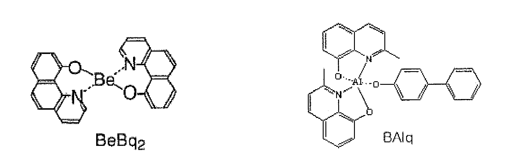
- A thickness of the ETL may preferably be in a range of about 100 to about 1,000 Å, for example, about 200 to about 500 Å. When the thickness of the ETL is within this range, the ETL may preferably have excellent electron transport properties without a substantial increase in driving voltage.
- The EIL may preferably be formed on the ETL. The EIL may preferably comprise any well-known electron injection material such as LiF, NaCl, CsF, Li2O, or BaO. Deposition conditions for forming the EIL may preferably vary according to a compound that is used to form the EIL, but may preferably be similar to those described with reference to the HIL.
- A thickness of the EIL may preferably be in a range of about 1 to about 100 Å, for example, about 5 to about 50 Å. When the thickness of the EIL is within this range, the EIL may preferably have satisfactory electron injection properties without a substantial increase in driving voltage.
- Next, the
second electrode 27 is formed on theorganic layer 25. - Meanwhile, for example, as shown in
FIG. 3C , theencapsulation substrate 30 is prepared. In this case, a width L12 of theencapsulation substrate 30 may preferably be determined in consideration of considering a width L11 (seeFIGS. 3A and3B ) of an area of thedevice substrate 10 inside thethird electrode 40. In order to realize an organic light-emitting apparatus of the present invention, for example, as illustrated inFIG. 1A , the width L12 of theencapsulation substrate 30 may preferably be determined to be the same as the width L11 of the area of thedevice substrate 10 inside thethird electrode 40. - Next, for example, as shown in
FIG. 3D , theencapsulation substrate 30 and thedevice substrate 10 are assembled so that theencapsulation substrate 30 covers the light-emitting area A, a sealingmember forming material 50a for forming the sealingmember 50 may preferably be provided between thedevice substrate 10 and theencapsulation substrate 30 is subjected to a first process D to form the sealingmember 50 that is provided in the non-emitting area inside thethird electrode 40 to surround the light-emitting area A, and thedevice substrate 10 and theencapsulation substrate 30 are attached to each other. - The first process D for forming the sealing
member 50 from the sealingmember forming material 50a may preferably vary according to the selected sealingmember forming material 50a. For example, the first process D may preferably be soft baking for removing a solvent included in the sealingmember forming material 50a, UV radiation and/or heat treatment for curing the sealingmember forming material 50a, or laser beam radiation, which is a kind of heat treatment, for melting the sealingmember forming material 50a. - For example, the providing of the sealing
member 50 for attaching thedevice substrate 10 and theencapsulation substrate 30 to each other may preferably be performed by at least one of i) providing an adhesive precursor between thedevice substrate 10 and theencapsulation substrate 30 and curing the adhesive precursor (by using, for example, UV radiation or heat treatment), ii) providing a glass frit precursor between thedevice substrate 10 and theencapsulation substrate 30 and performing heat treatment (for example, laser beam radiation), and iii) providing the silicon-based compound represented by Formula 1 between thedevice substrate 10 and theencapsulation substrate 30. Formula 1 is described above, and will not be described again here. - Meanwhile, the method of manufacturing the organic light-emitting apparatus may preferably further include a) creating a vacuum in the
space 60 between thedevice substrate 10 and theencapsulation substrate 30, b) providing a moisture-absorbing layer to thespace 60 between thedevice substrate 10 and theencapsulation substrate 30, and c) providing a filler to thespace 60 between thedevice substrate 10 and theencapsulation substrate 30. The filler is described in more detail above. - Here, the providing of the filler may preferably be performed, for example, after providing the filler to an inner area C of the
encapsulation substrate 30, for example inFIG. 3C , by attaching thedevice substrate 10 and theencapsulation substrate 30. -
FIG. 4A is a cross-sectional view illustrating an organic light-emitting apparatus (a cross-sectional view taken along line I-I' ofFIG. 4B ) according to another embodiment.FIG. 4B is a plan view of the organic light-emitting apparatus ofFIG. 4A , in which anencapsulation substrate 130, asecond electrode 127, anorganic layer 125, and an insulatinglayer 123 are not shown. The organic light-emitting apparatus illustrated inFIGS. 4A and4B includes adevice substrate 110, theencapsulation substrate 130, afirst electrode 121, the insulatinglayer 123, theorganic layer 125, thesecond electrode 127, a sealingmember 150, athird electrode 140 including afirst portion 140a, and afirst layer 170. Thefirst electrode 121, the insulatinglayer 123, theorganic layer 125, and thesecond electrode 127 may preferably constitute an organic light-emittingdevice 120. The organic light-emitting apparatus may preferably include aspace 160 between thedevice substrate 110 and theencapsulation substrate 130. - For information about the
device substrate 110, theencapsulation substrate 130, thefirst electrode 121, the insulatinglayer 123, theorganic layer 125, thesecond electrode 127, the sealingmember 150, thethird electrode 140 including thefirst portion 140a, and thespace 160 between thedevice substrate 110 and theencapsulation substrate 130 of the organic light-emitting apparatus ofFIGS. 4A and4B , thesubstrate 10, theencapsulation substrate 30, thefirst electrode 21, the insulatinglayer 23, theorganic layer 25, thesecond electrode 27, the sealingmember 50, thethird electrode 40 including thefirst portion 40a, and thespace 60 between thedevice substrate 10 and theencapsulation substrate 30 the embodiments discussed above, for example in respect ofFIGS. 1A and 1B , should be referred to. - In the organic light-emitting apparatus of
FIGS. 4A and4B , the sealingmember 150 and thefirst portion 140a of thethird electrode 140 are spaced apart from each other, and a space between the sealingmember 150 and thefirst portion 140a of thethird electrode 140 is filled with thefirst layer 170. Here, thefirst layer 170 may preferably include at least one of the silicon-based compounds represented by Formula 1 and the cured product of the silicon-based compound (and optionally, the SAM formed from the silicon-based compound). Formula I is described above, and will not be described again here. - Since the silicon-based compound may preferably provide very low surface energy, the surface energy of a surface, which is exposed to external air, of the
first layer 170 is very low. Accordingly, since moisture and/or oxygen is prevented by not only thethird electrode 140 but also thefirst layer 170, the organic light-emittingdevice 120 of the organic light-emitting apparatus ofFIGS. 4A and4B may preferably be effectively prevented from deteriorating due to the moisture and/or oxygen, thereby extending the lifetime of the organic light-emitting apparatus. - The organic light-emitting apparatus of
FIGS. 4A and4B may preferably be manufactured by attaching thedevice substrate 110 and theencapsulation substrate 130 so that the width L12 (seeFIG. 3C ) of theencapsulation substrate 130 is less than the width L11 (seeFIG. 3C ) of thedevice substrate 110 inside thethird electrode 140 and forming thefirst layer 170 in the space between the sealingmember 150 and thefirst portion 140a of thethird electrode 140. Thefirst layer 170 may preferably be formed by providing the silicon-based compound (and optionally, a solvent) represented by Formula 1 to the space formed between the sealingmember 150 and thefirst portion 140a of thethird electrode 140 by any well-known method, such as inkjet printing or nozzle printing, and performing an additional process such as soft baking, but the present embodiment is not limited thereto. -
FIG. 5 is a cross-sectional view illustrating an organic light-emitting apparatus according to another embodiment of the present invention. The organic light-emitting apparatus ofFIG. 5 includes adevice substrate 210, anencapsulation substrate 230, afirst electrode 221, an insulatinglayer 223, anorganic layer 225, asecond electrode 227, a sealingmember 250, athird electrode 240 including afirst portion 240a and asecond portion 240b, and afirst layer 270. Thefirst electrode 221, the insulatinglayer 223, theorganic layer 225, and thesecond electrode 227 may preferably constitute an organic light-emittingdevice 220. The organic light-emitting apparatus includes aspace 260 between thedevice substrate 210 and theencapsulation substrate 230. - For information about the
device substrate 210, theencapsulation substrate 230, thefirst electrode 221, the insulatinglayer 223, theorganic layer 225, thesecond electrode 227, the sealingmember 250, thefirst layer 270, thefirst portion 240a, thethird electrode 240, and thespace 260 between thedevice substrate 210 and theencapsulation substrate 230 of the organic light-emitting apparatus ofFIG. 5 , thedevice substrate 110, theencapsulation substrate 130, thefirst electrode 121, the insulatinglayer 123, theorganic layer 125, thesecond electrode 127, the sealingmember 150, thefirst layer 170, thefirst portion 140a, thethird electrode 140, and thespace 160 between thedevice substrate 110 and theencapsulation substrate 130 of the organic light-emitting apparatus the embodiments discussed above, for example in respect ofFIGS 1A and 1B andFIGS. 4A and4B , should be referred to.. .. - The
third electrode 240 of the organic light-emitting apparatus ofFIG. 5 includes thefirst portion 240a that surrounds the sealingmember 250, and further includes thesecond portion 240b that extends from thefirst portion 240a of thethird electrode 240 toward the sealingmember 250. The maximum thickness L2 of thefirst portion 240a of thethird electrode 240 and a maximum thickness L5 of thesecond portion 240b of thethird electrode 240 may preferably have a relationship of L2≥L5. - Since the
second portion 240b of thethird electrode 240 is formed, moisture and/or oxygen permeation may preferably be effectively prevented. - A method of manufacturing the organic light-emitting apparatus of the present invention, for example that displayed by
FIG. 5 , will be explained with reference toFIGS. 6A through 6D . - First, for example, as shown in
FIG. 6A , thedevice substrate 210 is prepared, and then thefirst electrode 221 and athird layer 241 are simultaneously formed. The forming of thefirst electrode 221 and thethird layer 241 may preferably be performed by simultaneously forming thefirst electrode 221 and thethird layer 241 without a separate process of forming thethird layer 241, like in the forming of thefirst electrode 21 and the third electrode 24 ofFIG. 3A . - Next, for example, as shown in
FIG. 6B , part of thethird layer 241 is patterned and thus the first portion 241a and thesecond portion 240b of thethird layer 241 are formed, thereby forming thethird electrode 240. Thefirst portion 240a and thesecond portion 240b may preferably be formed by a general patterning method such as laser etching or wet etching. - Next, for example, as shown in
FIG. 6C , the insulatinglayer 223, theorganic layer 225, and thesecond electrode 227 are sequentially formed, as explained in detail with reference toFIG. 3B . - Next, for example, as shown in
FIG. 6D , theencapsulation substrate 230 and thedevice substrate 210 are assembled so that a portion of theencapsulation substrate 230 extending toward thedevice substrate 210 is located on thesecond portion 240b of thethird electrode 240, the sealingmember 250 is provided between theencapsulation substrate 230 and the device substrate 210 (in detail, between theencapsulation substrate 230 and thesecond portion 240b of the third electrode 240), and theencapsulation substrate 230 and thedevice substrate 210 are attached, as explained in detail with reference toFIG. 3D . - Next, the
first layer 270 is formed in aspace 280 formed between the sealingmember 250 and thefirst portion 240a of thethird electrode 240, thereby completely manufacturing the organic light-emitting apparatus ofFIG. 5 . -
FIG. 7 is a cross-sectional view illustrating an organic light-emitting apparatus according to another embodiment. The organic light-emitting apparatus ofFIG. 7 includes adevice substrate 310, anencapsulation substrate 330, afirst electrode 321, an insulatinglayer 323. an organic layer 325, asecond electrode 327, a sealingmember 350, athird electrode 340 including afirst portion 340a, and ahole 311. Thefirst electrode 321, the insulatinglayer 323, the organic layer 325, and thesecond electrode 327 may preferably constitute an organic light-emittingdevice 320. The organic light-emitting apparatus includes aspace 360 between thedevice substrate 310 and theencapsulation substrate 330. - For information about the
device substrate 310, theencapsulation substrate 330, thefirst electrode 321, the insulatinglayer 323, the organic layer 325, thesecond electrode 327, the sealingmember 350, thefirst portion 340a, thethird electrode 340, and thespace 360 between thedevice substrate 310 and theencapsulation substrate 330 of the organic light-emitting apparatus ofFIG. 7 , thedevice substrate 10, theencapsulation substrate 30, thefirst electrode 21, the insulatinglayer 23, theorganic layer 25, thesecond electrode 27, the sealingmember 50, thefirst portion 40a, thethird electrode 40 and thespace 60 between thedevice substrate 10 and theencapsulation substrate 30 of the organic light-emitting apparatus ofFIGS. 1A and 1B are referred to. - The
device substrate 310 of the organic light-emitting apparatus ofFIG. 7 includes thehole 311 corresponding to the sealingmember 350. Accordingly, the sealingmember 350 is formed in thehole 311. Accordingly, since the sealingmember 350 may preferably be prevented from being exposed to external air, oxygen and/or moisture permeation through a side surface of the sealingmember 350 may preferably be effectively prevented. - The organic light-emitting apparatus of
FIG. 7 may preferably be manufactured by preparing thedevice substrate 310 in which thehole 311 is already formed. - Although the organic light-emitting apparatus and the method of manufacturing the same according to the present embodiments has been explained with reference to
FIGS. 1A through 7 , various modifications may be made. For example, a side surface of the sealingmember 250 and a side surface of thefirst portion 240a of thethird electrode 240 of the organic light-emitting apparatus ofFIG. 5 may preferably contact each other, and thedevice substrate 10 of the organic light-emitting apparatus ofFIG. 1 may preferably further include a hole corresponding to the sealingmember 50. - The organic light-emitting apparatus according to the present embodiments have a long lifetime because it substantially prevents moisture and/or oxygen permeation.
Claims (21)
- An organic light-emitting apparatus comprising:a device substrate comprising a light-emitting area and a non-emitting area;an encapsulation substrate covering the light-emitting area;a first electrode formed on the light-emitting area and disposed between the device substrate and the encapsulation substrate;an organic layer disposed between the encapsulation substrate and the first electrode;a second electrode disposed between the organic layer and the encapsulation substrate;a sealing member surrounding the light-emitting area; anda third electrode disposed on the non-emitting area outside the sealing member, comprising a first portion surrounding the sealing member, and comprising the same material as that of the first electrode.
- The organic light-emitting apparatus of claim 1, wherein each of the first electrode and the third electrode comprises at least one of a metal and a conductive oxide, optionally indium tin oxide (ITO).
- The organic light-emitting apparatus of claim 1 or claim 2, wherein the sealing member comprises at least one of an adhesive and a glass frit and/or at least one of a silicon-based compound represented by Formula 1 and a cured product of the silicon-based compound:
F-[Q1]a-O-[Q2-O]b-[Q3-O]c,-[Q4-O]d-[Q5]e-[Y1]fSi(Z1)g(Z2)3-g, <Formula 1>
wherein Q1 is a divalent group represented by -C(R1)(R2)-;
Q2 is a divalent group represented by -C(R3)(R4)-C(R5)(R6)-C(R7)(R8)-;
Q3 is a divalent group represented by -C(R9)(R10)-C(R11)(R12)-;
Q4 is a divalent group represented by -C(R13)(R14)-;
Q5 is a divalent group represented by -C(R15)(R16)-;
R1 through R16 are each independently selected from the group consisting of H, -F, -CH3, -CH2F, -CHF2, and -CF3;
Y1 is a divalent organic group;
Z1 is a C1-C30 alkyl group or a C1-C30 alkyl group that is substituted with at least one -F;
Z2 is a C1-C30 alkoxy group or a C1-C30 alkoxy group that is substituted with at least one -F;
a and e are each independently an integer from 1 to 20;
b, c, and d are each independently an integer from 0 to 200, and wherein b, c, and d are not all 0;
f is an integer from 0 to 10; and
g is an integer from 0 to 3. - The organic light-emitting apparatus of any of claims 1 to 3, wherein the sealing member sequentially comprises a first sealing member layer, a second sealing member layer, and a third sealing member layer, wherein each of the first sealing member layer and the third sealing member layer comprises an adhesive, and the second sealing member layer comprises at least one of a silicon-based compound represented by Formula 1 and a cured product of the silicon-based compound as defined in claim 3.
- The organic light-emitting apparatus of any of claims 1 to 4, wherein a side surface of the sealing member and a side surface of the first portion of the third electrode contact each other.
- The organic light-emitting apparatus of any of claims 1 to 5, wherein when a maximum thickness of the first electrode is L1 and a maximum thickness of the first portion of the third electrode is L2, L1=L2.
- The organic light-emitting apparatus of any of claims 1 to 6, wherein, when a maximum thickness of the first portion of the third electrode is L2 and a maximum thickness of the sealing member is L3, L2≥L3.
- The organic light-emitting apparatus of any of claims 1 to 7, wherein a space is present between the device substrate and the encapsulation substrate, optionally the space comprises a vacuum space, or a moisture-absorbing layer disposed in a space between the device substrate and the encapsulation substrate or a filler fills a space between the device substrate and the encapsulation substrate.
- The organic light-emitting apparatus of claim 8, wherein the filler comprises at least one of a silicon-based compound represented by Formula 1 and a cured product of the silicon-based compound as defined in claim 3
- The organic light-emitting apparatus of any of claims 1 to 9, wherein the sealing member and the first portion of the third electrode are spaced apart from each other, a space between the sealing member and the first portion of the third electrode is filled with a first layer, and the first layer comprises at least one of a silicon-based compound represented by Formula 1 and a cured product of the silicon-based compound as defined in claim 3.
- The organic light-emitting apparatus of claim 10, wherein, when a maximum thickness of the sealing member is L3 and a maximum thickness of the first layer is L4, L3≤L4.
- The organic light-emitting apparatus of any of claims 1 to 11, wherein the third electrode has a second portion extending from the first portion of the third electrode toward the sealing member, and the second portion of the third electrode is located between the sealing member and the device substrate.
- The organic light-emitting apparatus of claim 12, wherein, when a maximum thickness of the first portion of the third electrode is L2 and a maximum thickness of the second portion of the third electrode is L5, L2≥L5.
- The organic light-emitting apparatus of claim 12 or claim 13, wherein the sealing member and the first portion of the third electrode are spaced apart from each other, a space between the sealing member and the first portion of the third electrode is filled with a first layer, and the first layer comprises at least one of a silicon-based compound represented by Formula 1 and a cured product of the silicon-based compound as defined in claim 3.
- The organic light-emitting apparatus of any of claims 1 to 14, wherein the device substrate comprises a hole corresponding to the sealing member, and the sealing member is disposed in the hole.
- A method of manufacturing an organic light-emitting apparatus as claimed in any of claims 1 to 15, the method comprising:preparing a device substrate comprising a light-emitting area and a non-emitting area;forming a first electrode on the light-emitting area, and forming a third electrode comprising a first portion and comprising the same material as that of the first electrode on the non-emitting area;forming an organic layer on the first electrode;forming a second electrode on the organic layer, andattaching the device substrate and an encapsulation substrate to each other by assembling the encapsulation substrate with the device substrate so that the encapsulation substrate covers the light-emitting area, and providing a sealing member to the non-emitting area inside the third electrode to surround the light-emitting area.
- The method of claim 16, wherein the providing of the sealing member of the attaching of the device substrate and the encapsulation substrate to each other comprises at least one of; providing an adhesive precursor between the device substrate and the encapsulation substrate and curing the adhesive precursor, providing a glass frit precursor between the device substrate and the encapsulation substrate and performing heat treatment, and providing a silicon-based compound represented by Formula 1 as defined in claim 3. between the device substrate and the encapsulation substrate
- The method of claim 16 or claim 17, further comprising at least one of creating a vacuum in a space between the device substrate and the encapsulation substrate, providing a moisture-absorbing layer to the space between the device substrate and the encapsulation substrate, and providing a filler to the space between the device substrate and the encapsulation substrate.
- The method of any of claims 16 to 18, further comprising, after the attaching of the device substrate and the encapsulation substrate to each other, providing a first layer comprising at least one of a silicon-based compound represented by Formula 1 and a cured product of the silicon-based compound as defined in claim 3 to a space between the sealing member and the first portion of the third electrode.
- The method of any of claims 16 to 19, wherein the forming of the first electrode and the third electrode further comprises additionally forming a second portion extending from the first portion of the third electrode toward the sealing member.
- The method of any of claims 16 to 19, wherein the providing of the device substrate comprising the light-emitting area and the non-emitting area further comprises forming a hole corresponding to the sealing member in the non-emitting area of the device substrate.
Applications Claiming Priority (1)
| Application Number | Priority Date | Filing Date | Title |
|---|---|---|---|
| KR1020100066997A KR101193198B1 (en) | 2010-07-12 | 2010-07-12 | Organic light emitting device and method for preparing the same |
Publications (3)
| Publication Number | Publication Date |
|---|---|
| EP2408038A2 true EP2408038A2 (en) | 2012-01-18 |
| EP2408038A3 EP2408038A3 (en) | 2013-05-29 |
| EP2408038B1 EP2408038B1 (en) | 2017-03-29 |
Family
ID=44680934
Family Applications (1)
| Application Number | Title | Priority Date | Filing Date |
|---|---|---|---|
| EP11173649.2A Not-in-force EP2408038B1 (en) | 2010-07-12 | 2011-07-12 | Organic light-emitting apparatus and method of manufacturing the same |
Country Status (6)
| Country | Link |
|---|---|
| US (1) | US9105870B2 (en) |
| EP (1) | EP2408038B1 (en) |
| JP (1) | JP5877966B2 (en) |
| KR (1) | KR101193198B1 (en) |
| CN (1) | CN102332464B (en) |
| TW (1) | TWI511973B (en) |
Families Citing this family (6)
| Publication number | Priority date | Publication date | Assignee | Title |
|---|---|---|---|---|
| US20150041783A1 (en) * | 2012-02-13 | 2015-02-12 | Panasonic Corporation | Organic electroluminescence element |
| KR102103421B1 (en) | 2013-02-07 | 2020-04-23 | 삼성디스플레이 주식회사 | Organic light emitting diode device and manufacturing method thereof |
| US9985209B2 (en) * | 2014-03-17 | 2018-05-29 | Joled Inc. | Method for testing lifetime characteristics of display panel, and method for manufacturing display panel |
| DE102014106885B4 (en) * | 2014-05-15 | 2022-01-20 | Pictiva Displays International Limited | Method for producing an insulator layer, method for producing an organic optoelectronic component comprising an insulator layer and organic optoelectronic component comprising an insulator layer |
| JP6563796B2 (en) * | 2015-12-03 | 2019-08-21 | 双葉電子工業株式会社 | Sealing structure, organic EL display device, and sensor |
| KR20220034949A (en) * | 2020-09-11 | 2022-03-21 | 삼성디스플레이 주식회사 | Display device |
Citations (1)
| Publication number | Priority date | Publication date | Assignee | Title |
|---|---|---|---|---|
| KR20100066997A (en) | 2008-12-10 | 2010-06-18 | 손석훈 | Move network node |
Family Cites Families (32)
| Publication number | Priority date | Publication date | Assignee | Title |
|---|---|---|---|---|
| US5990615A (en) | 1997-02-03 | 1999-11-23 | Nec Corporation | Organic electroluminescent display with protective layer on cathode and an inert medium |
| KR100269391B1 (en) | 1998-07-28 | 2000-10-16 | 구자홍 | Organic electroluminescence device |
| US6900590B2 (en) | 2000-10-17 | 2005-05-31 | Samsung Sdi Co., Ltd. | Organic electroluminescent device having non-continuous metal auxiliary electrodes |
| JP2003217832A (en) | 2002-01-28 | 2003-07-31 | Mitsumi Electric Co Ltd | Method for manufacturing organic electroluminescence element and organic electroluminescence display |
| KR100577619B1 (en) | 2003-03-05 | 2006-05-10 | 엘지전자 주식회사 | Organic electroluminescent element and getter forming mask formed therein |
| US7109654B2 (en) | 2003-03-14 | 2006-09-19 | Samsung Sdi Co., Ltd. | Electroluminescence device |
| KR100522689B1 (en) | 2003-03-14 | 2005-10-20 | 삼성에스디아이 주식회사 | Electroluminescence device |
| US20040206953A1 (en) | 2003-04-16 | 2004-10-21 | Robert Morena | Hermetically sealed glass package and method of fabrication |
| US20050116245A1 (en) * | 2003-04-16 | 2005-06-02 | Aitken Bruce G. | Hermetically sealed glass package and method of fabrication |
| JP2004327402A (en) | 2003-04-28 | 2004-11-18 | Kureha Chem Ind Co Ltd | Moisture-proof electroluminescent element and its manufacturing method |
| JP4534064B2 (en) | 2003-08-27 | 2010-09-01 | 奇美電子股▲ふん▼有限公司 | Manufacturing method of organic EL display |
| JP2005078906A (en) | 2003-08-29 | 2005-03-24 | Nippon Seiki Co Ltd | Organic EL panel |
| KR100635049B1 (en) * | 2003-11-29 | 2006-10-17 | 삼성에스디아이 주식회사 | Organic electroluminescent display |
| JP2005243376A (en) * | 2004-02-26 | 2005-09-08 | Nippon Seiki Co Ltd | Organic EL panel and manufacturing method thereof |
| KR20060023652A (en) | 2004-09-10 | 2006-03-15 | (주)케이디티 | Encapsulation technology of an organic light emitting display device using a film absorber |
| KR20060084743A (en) | 2005-01-20 | 2006-07-25 | (주)네스디스플레이 | Manufacturing method of organic electroluminescent device having a thin film type encapsulation structure |
| JP2006202650A (en) | 2005-01-21 | 2006-08-03 | Seiko Epson Corp | Electro-optical device and image printing device |
| KR20060084978A (en) | 2005-01-21 | 2006-07-26 | 에스케이씨 주식회사 | Structure and method of UV blocking bag of organic light emitting diode device |
| US8481668B2 (en) | 2005-09-16 | 2013-07-09 | Momentive Performance Materials Inc. | Silane-containing adhesion promoter composition and sealants, adhesives and coatings containing same |
| JP2007284472A (en) | 2006-04-12 | 2007-11-01 | Shin Etsu Chem Co Ltd | End seal material |
| KR101233144B1 (en) * | 2006-06-12 | 2013-02-14 | 엘지디스플레이 주식회사 | Organic electro-luminescence device and method for fabricating the same |
| JP2008016300A (en) | 2006-07-05 | 2008-01-24 | Seiko Epson Corp | Organic light emitting device manufacturing method, organic light emitting device, and electronic apparatus |
| KR100730225B1 (en) | 2006-08-01 | 2007-06-19 | 삼성에스디아이 주식회사 | Flat panel display |
| JP2008218206A (en) | 2007-03-05 | 2008-09-18 | Seiko Epson Corp | Electro-optical device, manufacturing method thereof, and electronic apparatus |
| KR101311670B1 (en) | 2007-07-09 | 2013-09-25 | 엘지디스플레이 주식회사 | Organic Electroluminescent Device and method for fabricating thereof |
| KR101376319B1 (en) | 2007-07-27 | 2014-03-20 | 주식회사 동진쎄미켐 | A sealing method for display element |
| JP2009134274A (en) | 2007-10-30 | 2009-06-18 | Semiconductor Energy Lab Co Ltd | Liquid crystal display and method for manufacturing the same |
| KR100940086B1 (en) | 2007-12-13 | 2010-02-02 | 한국화학연구원 | Perfluorinated Polyether Modified Silane Compound and Antifouling Coating Composition Containing the Same and Membrane Applying the Same |
| JP2009163081A (en) | 2008-01-09 | 2009-07-23 | Citizen Holdings Co Ltd | Liquid crystal device and its manufacturing method |
| JPWO2009139292A1 (en) | 2008-05-12 | 2011-09-22 | コイズミ照明株式会社 | Organic EL light emitting device and method for manufacturing the same |
| JP2010080341A (en) | 2008-09-26 | 2010-04-08 | Toshiba Mobile Display Co Ltd | Display |
| JP2010121144A (en) | 2008-11-17 | 2010-06-03 | Seiko Epson Corp | Film-forming apparatus |
-
2010
- 2010-07-12 KR KR1020100066997A patent/KR101193198B1/en not_active Expired - Fee Related
-
2011
- 2011-06-07 US US13/155,296 patent/US9105870B2/en not_active Expired - Fee Related
- 2011-07-11 TW TW100124507A patent/TWI511973B/en not_active IP Right Cessation
- 2011-07-12 EP EP11173649.2A patent/EP2408038B1/en not_active Not-in-force
- 2011-07-12 CN CN201110199190.0A patent/CN102332464B/en active Active
- 2011-07-12 JP JP2011154242A patent/JP5877966B2/en not_active Expired - Fee Related
Patent Citations (1)
| Publication number | Priority date | Publication date | Assignee | Title |
|---|---|---|---|---|
| KR20100066997A (en) | 2008-12-10 | 2010-06-18 | 손석훈 | Move network node |
Also Published As
| Publication number | Publication date |
|---|---|
| KR20120006328A (en) | 2012-01-18 |
| US20120007137A1 (en) | 2012-01-12 |
| CN102332464B (en) | 2016-06-08 |
| JP5877966B2 (en) | 2016-03-08 |
| US9105870B2 (en) | 2015-08-11 |
| JP2012023038A (en) | 2012-02-02 |
| CN102332464A (en) | 2012-01-25 |
| TWI511973B (en) | 2015-12-11 |
| EP2408038B1 (en) | 2017-03-29 |
| TW201211056A (en) | 2012-03-16 |
| KR101193198B1 (en) | 2012-10-26 |
| EP2408038A3 (en) | 2013-05-29 |
Similar Documents
| Publication | Publication Date | Title |
|---|---|---|
| EP2312668B1 (en) | Organic light-emitting diode and method of manufacturing the same | |
| EP2202821B1 (en) | Organic light emitting apparatus and method of manufacturing the same | |
| US7892878B2 (en) | Organic light emitting device and method of manufacturing the same | |
| US8168967B2 (en) | Organic light emitting device and method of manufacturing the same | |
| USRE47578E1 (en) | Organic light-emitting device and of preparing the same | |
| EP2408038B1 (en) | Organic light-emitting apparatus and method of manufacturing the same | |
| CN104241537B (en) | Organic light emitting apparatus including auxiliary electrode | |
| CN101252171B (en) | Organic light emitting device, method of manufacturing the same, and method of forming organic layer | |
| US10522778B2 (en) | Organic light-emitting diode including an electronic transport layer comprising a three component blend of a matrix compound and two lithium compounds | |
| WO2005002286A1 (en) | Organic electroluminescence element, process for fabricating the same and electrode film | |
| US20120012828A1 (en) | Organic light-emitting device | |
| US20110248259A1 (en) | Organic light emitting device and method of manufacturing the same | |
| KR101174886B1 (en) | Organic light emitting device and method for preparing the same | |
| KR100813853B1 (en) | Organic light emitting device and method for manufacturing same | |
| US20110193068A1 (en) | Composite film, flexible substrate including the composite film, and organic light emitting device including the flexible substrate |
Legal Events
| Date | Code | Title | Description |
|---|---|---|---|
| AK | Designated contracting states |
Kind code of ref document: A2 Designated state(s): AL AT BE BG CH CY CZ DE DK EE ES FI FR GB GR HR HU IE IS IT LI LT LU LV MC MK MT NL NO PL PT RO RS SE SI SK SM TR |
|
| AX | Request for extension of the european patent |
Extension state: BA ME |
|
| PUAI | Public reference made under article 153(3) epc to a published international application that has entered the european phase |
Free format text: ORIGINAL CODE: 0009012 |
|
| RAP1 | Party data changed (applicant data changed or rights of an application transferred) |
Owner name: SAMSUNG DISPLAY CO., LTD. |
|
| PUAL | Search report despatched |
Free format text: ORIGINAL CODE: 0009013 |
|
| AK | Designated contracting states |
Kind code of ref document: A3 Designated state(s): AL AT BE BG CH CY CZ DE DK EE ES FI FR GB GR HR HU IE IS IT LI LT LU LV MC MK MT NL NO PL PT RO RS SE SI SK SM TR |
|
| AX | Request for extension of the european patent |
Extension state: BA ME |
|
| RIC1 | Information provided on ipc code assigned before grant |
Ipc: H01L 51/00 20060101ALN20130423BHEP Ipc: H01L 51/52 20060101AFI20130423BHEP |
|
| 17P | Request for examination filed |
Effective date: 20130716 |
|
| RBV | Designated contracting states (corrected) |
Designated state(s): AL AT BE BG CH CY CZ DE DK EE ES FI FR GB GR HR HU IE IS IT LI LT LU LV MC MK MT NL NO PL PT RO RS SE SI SK SM TR |
|
| RAP1 | Party data changed (applicant data changed or rights of an application transferred) |
Owner name: SAMSUNG DISPLAY CO., LTD. |
|
| 17Q | First examination report despatched |
Effective date: 20151014 |
|
| GRAP | Despatch of communication of intention to grant a patent |
Free format text: ORIGINAL CODE: EPIDOSNIGR1 |
|
| RIC1 | Information provided on ipc code assigned before grant |
Ipc: H01L 51/00 20060101ALN20160707BHEP Ipc: H01L 51/52 20060101AFI20160707BHEP |
|
| INTG | Intention to grant announced |
Effective date: 20160803 |
|
| RIC1 | Information provided on ipc code assigned before grant |
Ipc: H01L 51/00 20060101ALN20160725BHEP Ipc: H01L 51/52 20060101AFI20160725BHEP |
|
| GRAS | Grant fee paid |
Free format text: ORIGINAL CODE: EPIDOSNIGR3 |
|
| GRAJ | Information related to disapproval of communication of intention to grant by the applicant or resumption of examination proceedings by the epo deleted |
Free format text: ORIGINAL CODE: EPIDOSDIGR1 |
|
| GRAL | Information related to payment of fee for publishing/printing deleted |
Free format text: ORIGINAL CODE: EPIDOSDIGR3 |
|
| INTC | Intention to grant announced (deleted) | ||
| GRAR | Information related to intention to grant a patent recorded |
Free format text: ORIGINAL CODE: EPIDOSNIGR71 |
|
| GRAA | (expected) grant |
Free format text: ORIGINAL CODE: 0009210 |
|
| RIC1 | Information provided on ipc code assigned before grant |
Ipc: H01L 51/52 20060101AFI20170207BHEP Ipc: H01L 51/00 20060101ALN20170207BHEP |
|
| AK | Designated contracting states |
Kind code of ref document: B1 Designated state(s): AL AT BE BG CH CY CZ DE DK EE ES FI FR GB GR HR HU IE IS IT LI LT LU LV MC MK MT NL NO PL PT RO RS SE SI SK SM TR |
|
| INTG | Intention to grant announced |
Effective date: 20170222 |
|
| REG | Reference to a national code |
Ref country code: GB Ref legal event code: FG4D |
|
| REG | Reference to a national code |
Ref country code: CH Ref legal event code: EP |
|
| REG | Reference to a national code |
Ref country code: AT Ref legal event code: REF Ref document number: 880501 Country of ref document: AT Kind code of ref document: T Effective date: 20170415 |
|
| REG | Reference to a national code |
Ref country code: IE Ref legal event code: FG4D |
|
| REG | Reference to a national code |
Ref country code: DE Ref legal event code: R096 Ref document number: 602011036389 Country of ref document: DE |
|
| PG25 | Lapsed in a contracting state [announced via postgrant information from national office to epo] |
Ref country code: FI Free format text: LAPSE BECAUSE OF FAILURE TO SUBMIT A TRANSLATION OF THE DESCRIPTION OR TO PAY THE FEE WITHIN THE PRESCRIBED TIME-LIMIT Effective date: 20170329 Ref country code: HR Free format text: LAPSE BECAUSE OF FAILURE TO SUBMIT A TRANSLATION OF THE DESCRIPTION OR TO PAY THE FEE WITHIN THE PRESCRIBED TIME-LIMIT Effective date: 20170329 Ref country code: NO Free format text: LAPSE BECAUSE OF FAILURE TO SUBMIT A TRANSLATION OF THE DESCRIPTION OR TO PAY THE FEE WITHIN THE PRESCRIBED TIME-LIMIT Effective date: 20170629 Ref country code: LT Free format text: LAPSE BECAUSE OF FAILURE TO SUBMIT A TRANSLATION OF THE DESCRIPTION OR TO PAY THE FEE WITHIN THE PRESCRIBED TIME-LIMIT Effective date: 20170329 Ref country code: GR Free format text: LAPSE BECAUSE OF FAILURE TO SUBMIT A TRANSLATION OF THE DESCRIPTION OR TO PAY THE FEE WITHIN THE PRESCRIBED TIME-LIMIT Effective date: 20170630 |
|
| REG | Reference to a national code |
Ref country code: NL Ref legal event code: MP Effective date: 20170329 |
|
| REG | Reference to a national code |
Ref country code: AT Ref legal event code: MK05 Ref document number: 880501 Country of ref document: AT Kind code of ref document: T Effective date: 20170329 |
|
| PG25 | Lapsed in a contracting state [announced via postgrant information from national office to epo] |
Ref country code: RS Free format text: LAPSE BECAUSE OF FAILURE TO SUBMIT A TRANSLATION OF THE DESCRIPTION OR TO PAY THE FEE WITHIN THE PRESCRIBED TIME-LIMIT Effective date: 20170329 Ref country code: LV Free format text: LAPSE BECAUSE OF FAILURE TO SUBMIT A TRANSLATION OF THE DESCRIPTION OR TO PAY THE FEE WITHIN THE PRESCRIBED TIME-LIMIT Effective date: 20170329 Ref country code: BG Free format text: LAPSE BECAUSE OF FAILURE TO SUBMIT A TRANSLATION OF THE DESCRIPTION OR TO PAY THE FEE WITHIN THE PRESCRIBED TIME-LIMIT Effective date: 20170629 Ref country code: SE Free format text: LAPSE BECAUSE OF FAILURE TO SUBMIT A TRANSLATION OF THE DESCRIPTION OR TO PAY THE FEE WITHIN THE PRESCRIBED TIME-LIMIT Effective date: 20170329 |
|
| PG25 | Lapsed in a contracting state [announced via postgrant information from national office to epo] |
Ref country code: NL Free format text: LAPSE BECAUSE OF FAILURE TO SUBMIT A TRANSLATION OF THE DESCRIPTION OR TO PAY THE FEE WITHIN THE PRESCRIBED TIME-LIMIT Effective date: 20170329 |
|
| PG25 | Lapsed in a contracting state [announced via postgrant information from national office to epo] |
Ref country code: RO Free format text: LAPSE BECAUSE OF FAILURE TO SUBMIT A TRANSLATION OF THE DESCRIPTION OR TO PAY THE FEE WITHIN THE PRESCRIBED TIME-LIMIT Effective date: 20170329 Ref country code: AT Free format text: LAPSE BECAUSE OF FAILURE TO SUBMIT A TRANSLATION OF THE DESCRIPTION OR TO PAY THE FEE WITHIN THE PRESCRIBED TIME-LIMIT Effective date: 20170329 Ref country code: SK Free format text: LAPSE BECAUSE OF FAILURE TO SUBMIT A TRANSLATION OF THE DESCRIPTION OR TO PAY THE FEE WITHIN THE PRESCRIBED TIME-LIMIT Effective date: 20170329 Ref country code: CZ Free format text: LAPSE BECAUSE OF FAILURE TO SUBMIT A TRANSLATION OF THE DESCRIPTION OR TO PAY THE FEE WITHIN THE PRESCRIBED TIME-LIMIT Effective date: 20170329 Ref country code: IT Free format text: LAPSE BECAUSE OF FAILURE TO SUBMIT A TRANSLATION OF THE DESCRIPTION OR TO PAY THE FEE WITHIN THE PRESCRIBED TIME-LIMIT Effective date: 20170329 Ref country code: ES Free format text: LAPSE BECAUSE OF FAILURE TO SUBMIT A TRANSLATION OF THE DESCRIPTION OR TO PAY THE FEE WITHIN THE PRESCRIBED TIME-LIMIT Effective date: 20170329 Ref country code: EE Free format text: LAPSE BECAUSE OF FAILURE TO SUBMIT A TRANSLATION OF THE DESCRIPTION OR TO PAY THE FEE WITHIN THE PRESCRIBED TIME-LIMIT Effective date: 20170329 |
|
| PG25 | Lapsed in a contracting state [announced via postgrant information from national office to epo] |
Ref country code: SM Free format text: LAPSE BECAUSE OF FAILURE TO SUBMIT A TRANSLATION OF THE DESCRIPTION OR TO PAY THE FEE WITHIN THE PRESCRIBED TIME-LIMIT Effective date: 20170329 Ref country code: PL Free format text: LAPSE BECAUSE OF FAILURE TO SUBMIT A TRANSLATION OF THE DESCRIPTION OR TO PAY THE FEE WITHIN THE PRESCRIBED TIME-LIMIT Effective date: 20170329 Ref country code: PT Free format text: LAPSE BECAUSE OF FAILURE TO SUBMIT A TRANSLATION OF THE DESCRIPTION OR TO PAY THE FEE WITHIN THE PRESCRIBED TIME-LIMIT Effective date: 20170731 Ref country code: IS Free format text: LAPSE BECAUSE OF FAILURE TO SUBMIT A TRANSLATION OF THE DESCRIPTION OR TO PAY THE FEE WITHIN THE PRESCRIBED TIME-LIMIT Effective date: 20170729 |
|
| REG | Reference to a national code |
Ref country code: DE Ref legal event code: R097 Ref document number: 602011036389 Country of ref document: DE |
|
| PG25 | Lapsed in a contracting state [announced via postgrant information from national office to epo] |
Ref country code: DK Free format text: LAPSE BECAUSE OF FAILURE TO SUBMIT A TRANSLATION OF THE DESCRIPTION OR TO PAY THE FEE WITHIN THE PRESCRIBED TIME-LIMIT Effective date: 20170329 |
|
| PLBE | No opposition filed within time limit |
Free format text: ORIGINAL CODE: 0009261 |
|
| STAA | Information on the status of an ep patent application or granted ep patent |
Free format text: STATUS: NO OPPOSITION FILED WITHIN TIME LIMIT |
|
| REG | Reference to a national code |
Ref country code: CH Ref legal event code: PL |
|
| 26N | No opposition filed |
Effective date: 20180103 |
|
| REG | Reference to a national code |
Ref country code: IE Ref legal event code: MM4A |
|
| REG | Reference to a national code |
Ref country code: FR Ref legal event code: ST Effective date: 20180330 |
|
| PG25 | Lapsed in a contracting state [announced via postgrant information from national office to epo] |
Ref country code: IE Free format text: LAPSE BECAUSE OF NON-PAYMENT OF DUE FEES Effective date: 20170712 Ref country code: CH Free format text: LAPSE BECAUSE OF NON-PAYMENT OF DUE FEES Effective date: 20170731 Ref country code: LI Free format text: LAPSE BECAUSE OF NON-PAYMENT OF DUE FEES Effective date: 20170731 |
|
| PG25 | Lapsed in a contracting state [announced via postgrant information from national office to epo] |
Ref country code: FR Free format text: LAPSE BECAUSE OF NON-PAYMENT OF DUE FEES Effective date: 20170731 Ref country code: SI Free format text: LAPSE BECAUSE OF FAILURE TO SUBMIT A TRANSLATION OF THE DESCRIPTION OR TO PAY THE FEE WITHIN THE PRESCRIBED TIME-LIMIT Effective date: 20170329 |
|
| REG | Reference to a national code |
Ref country code: BE Ref legal event code: MM Effective date: 20170731 |
|
| PG25 | Lapsed in a contracting state [announced via postgrant information from national office to epo] |
Ref country code: LU Free format text: LAPSE BECAUSE OF NON-PAYMENT OF DUE FEES Effective date: 20170712 |
|
| PG25 | Lapsed in a contracting state [announced via postgrant information from national office to epo] |
Ref country code: BE Free format text: LAPSE BECAUSE OF NON-PAYMENT OF DUE FEES Effective date: 20170731 |
|
| PG25 | Lapsed in a contracting state [announced via postgrant information from national office to epo] |
Ref country code: MT Free format text: LAPSE BECAUSE OF NON-PAYMENT OF DUE FEES Effective date: 20170712 |
|
| PG25 | Lapsed in a contracting state [announced via postgrant information from national office to epo] |
Ref country code: MC Free format text: LAPSE BECAUSE OF FAILURE TO SUBMIT A TRANSLATION OF THE DESCRIPTION OR TO PAY THE FEE WITHIN THE PRESCRIBED TIME-LIMIT Effective date: 20170329 Ref country code: HU Free format text: LAPSE BECAUSE OF FAILURE TO SUBMIT A TRANSLATION OF THE DESCRIPTION OR TO PAY THE FEE WITHIN THE PRESCRIBED TIME-LIMIT; INVALID AB INITIO Effective date: 20110712 |
|
| PG25 | Lapsed in a contracting state [announced via postgrant information from national office to epo] |
Ref country code: CY Free format text: LAPSE BECAUSE OF NON-PAYMENT OF DUE FEES Effective date: 20170329 |
|
| PGFP | Annual fee paid to national office [announced via postgrant information from national office to epo] |
Ref country code: GB Payment date: 20190621 Year of fee payment: 9 Ref country code: DE Payment date: 20190620 Year of fee payment: 9 |
|
| PG25 | Lapsed in a contracting state [announced via postgrant information from national office to epo] |
Ref country code: MK Free format text: LAPSE BECAUSE OF FAILURE TO SUBMIT A TRANSLATION OF THE DESCRIPTION OR TO PAY THE FEE WITHIN THE PRESCRIBED TIME-LIMIT Effective date: 20170329 |
|
| PG25 | Lapsed in a contracting state [announced via postgrant information from national office to epo] |
Ref country code: TR Free format text: LAPSE BECAUSE OF FAILURE TO SUBMIT A TRANSLATION OF THE DESCRIPTION OR TO PAY THE FEE WITHIN THE PRESCRIBED TIME-LIMIT Effective date: 20170329 |
|
| PG25 | Lapsed in a contracting state [announced via postgrant information from national office to epo] |
Ref country code: AL Free format text: LAPSE BECAUSE OF FAILURE TO SUBMIT A TRANSLATION OF THE DESCRIPTION OR TO PAY THE FEE WITHIN THE PRESCRIBED TIME-LIMIT Effective date: 20170329 |
|
| REG | Reference to a national code |
Ref country code: DE Ref legal event code: R119 Ref document number: 602011036389 Country of ref document: DE |
|
| GBPC | Gb: european patent ceased through non-payment of renewal fee |
Effective date: 20200712 |
|
| PG25 | Lapsed in a contracting state [announced via postgrant information from national office to epo] |
Ref country code: GB Free format text: LAPSE BECAUSE OF NON-PAYMENT OF DUE FEES Effective date: 20200712 |
|
| PG25 | Lapsed in a contracting state [announced via postgrant information from national office to epo] |
Ref country code: DE Free format text: LAPSE BECAUSE OF NON-PAYMENT OF DUE FEES Effective date: 20210202 |