EP2406771B1 - Dokumentvalidierer mit powermanagement - Google Patents
Dokumentvalidierer mit powermanagement Download PDFInfo
- Publication number
- EP2406771B1 EP2406771B1 EP10713747.3A EP10713747A EP2406771B1 EP 2406771 B1 EP2406771 B1 EP 2406771B1 EP 10713747 A EP10713747 A EP 10713747A EP 2406771 B1 EP2406771 B1 EP 2406771B1
- Authority
- EP
- European Patent Office
- Prior art keywords
- validator
- power
- fet
- unit
- wake
- Prior art date
- Legal status (The legal status is an assumption and is not a legal conclusion. Google has not performed a legal analysis and makes no representation as to the accuracy of the status listed.)
- Not-in-force
Links
- 238000001514 detection method Methods 0.000 claims description 13
- 238000000034 method Methods 0.000 claims description 8
- 238000012545 processing Methods 0.000 claims description 6
- 230000007704 transition Effects 0.000 claims description 5
- 238000005259 measurement Methods 0.000 claims description 2
- 238000010200 validation analysis Methods 0.000 description 8
- 238000012546 transfer Methods 0.000 description 4
- 238000012544 monitoring process Methods 0.000 description 2
- 230000004044 response Effects 0.000 description 2
- 230000008901 benefit Effects 0.000 description 1
- 235000013361 beverage Nutrition 0.000 description 1
- 230000001419 dependent effect Effects 0.000 description 1
- 230000005669 field effect Effects 0.000 description 1
- 230000007246 mechanism Effects 0.000 description 1
- 230000003287 optical effect Effects 0.000 description 1
- 230000009467 reduction Effects 0.000 description 1
- 238000005057 refrigeration Methods 0.000 description 1
Images


Classifications
-
- G—PHYSICS
- G07—CHECKING-DEVICES
- G07D—HANDLING OF COINS OR VALUABLE PAPERS, e.g. TESTING, SORTING BY DENOMINATIONS, COUNTING, DISPENSING, CHANGING OR DEPOSITING
- G07D11/00—Devices accepting coins; Devices accepting, dispensing, sorting or counting valuable papers
- G07D11/20—Controlling or monitoring the operation of devices; Data handling
- G07D11/22—Means for sensing or detection
-
- G—PHYSICS
- G07—CHECKING-DEVICES
- G07D—HANDLING OF COINS OR VALUABLE PAPERS, e.g. TESTING, SORTING BY DENOMINATIONS, COUNTING, DISPENSING, CHANGING OR DEPOSITING
- G07D11/00—Devices accepting coins; Devices accepting, dispensing, sorting or counting valuable papers
- G07D11/40—Device architecture, e.g. modular construction
Definitions
- the disclosure relates to a device for validating documents of value (e.g., paper currency).
- value e.g., paper currency
- Bill validators are used in a wide variety of applications including; vending machines, gaming machines, ticketing machines and automated teller machines.
- Bill validators typically include a sensing unit for sensing authenticity and denomination of inserted banknotes.
- Various types of sensing systems can be employed by a bill validation device for example, optical sensing, magnetic sensing or a combination of both.
- Typical bill validation devices have power provided for operation either from the host machine or from a direct power source such as a standard AC power outlet.
- a limitation of the type of bill validator described above is that it is in a continuously "ON" mode and thus continually draws power either from the host machine or through a directly connected power source. As overall power consumption for a host machine is becoming more of an issue due to operation costs, there is a need to reduce such consumption.
- U1 discloses vending machine having a bill acceptance device comprising a main body and a circuit arrangement, wherein the main body comprises an inlet to receive a bill or a license and a bill box at the rear end of the inlet passage and wherein the main body further comprises an energy saving power supply module controlling the vending machine such that the vending machine enters an operational mode from a back-up mode when the validity of a bill or license is detected at the inlet of the acceptance device.
- a low power validator for validating documents of value is described in claim 1.
- a method for controlling the operation of a low power validator is described in claim 9. Examples are described in the dependent claims.
- the disclosure relates to a low power validator for documents of value (e.g., paper currency validator) and, in particular, to a battery powered banknote validator including a power management system for minimizing or reducing the power consumption from a power source.
- documents of value includes paper currency such as banknotes and bills, as well as security documents, paper coupons and other similar documents of value (both authentic as well as unauthentic (e.g., forgeries).
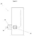
- a banknote validation device 10 includes an inlet 50 for receiving banknotes from a user, a transportation path 40 for conveying an inserted banknote within the bill validation device, a sensing unit 20 for sensing characteristics of an inserted banknote, and a processing unit for controlling the overall operation of the banknote validator.
- the sensing unit 20 and other components can be integrated, for example, within the processing unit.
- a power supply unit 70 and a power management system 100 there is provided with banknote validator 10 a power supply unit 70 and a power management system 100.
- power supply unit 70 is a 12-volt battery; however, other types of power supplies and voltages can be used for the power supply unit.
- Power management system 100 provides control of the supply power being fed to the banknote validator. More specifically, power management system 100 controls the transfer of the banknote validator from a power saving mode to a normal operation mode. In the power saving mode, overall banknote validation system 10 draws a very low amount of power from the power supply unit. In the normal operating mode, overall banknote validation system 10 draws a normal amount of power consistent with typical banknote validator operation. In some implementations, power management system 100 is located between power supply unit 70 and banknote validator 10. In other implementations, power management system 100 is integrated within banknote validator 10.
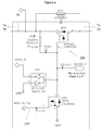
- power management system 100 includes a wake up unit 130 and a power detection unit 150.
- Wake up unit 130 includes a micro-controller 135 (e.g., a programmable system on chip or PSoC device) operatively connected to power source 70, power detection unit 150, and banknote validator 10.
- micro-controller 135 is a PSoC device.
- Figure 4 shows the interconnection of wake up unit 130, power detection unit 150 and banknote validator 10.
- FET 200 When validator 10 is in the power saving mode, FET 200 is in a disable mode so as to not provide main power to validator 10 via line 75. FET 200 is forced to a disable mode removing the connection of main power line 75 with validator 10 when output line 137 from microcontroller 135 becomes low.
- wake up circuit 130 regularly monitors inlet 50 of banknote validator 10 for the presence of a banknote.
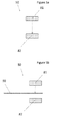
- the monitoring of inlet 50 for a banknote can be done in various ways known in the art, but for the example in Figures 5a and 5b is implemented as a paired photo-emitter 81 and photo-detector 82 arranged on either side of bill path 40.
- Emitter 81 continuously emits (e.g., infrared light) across the transportation path 40 of inlet 50 such that when no banknote is present, the emitted light from emitter 81 is received by detector 82.
- detector 82 receives light from emitter 81 a banknote is not present and, therefore, measuring the signal presence of detector 82 allows for determining there is no banknote present in inlet 50 of banknote validator 10.
- measuring the response signal of detector 92 allows for a determination of the presence of a banknote 90 in inlet 50.
- a reflective object sensor configuration can be used to detect the presence of banknote 90 in inlet 50.
- emitter 81 and detector 82 are located on the same side of banknote path 40.
- the presence of a banknote causes the light emitted from emitter 81 to be reflected by banknote 90 and thus received by detector 82. Having a signal received by detector 82 allows for the measurement of the response signal of detector 82 to determine the presence of a banknote in inlet 50 as previously described.
- Wake up unit 130 controls the banknote detection operation by driving emitter 81 (e.g., at a frequency of 10 Hz) and regularly samples (e.g., every 100 ms) for a received signal by detector 82 to determine if a banknote has been inserted in to inlet 50 by a user via lines 132, 131 respectively.
- wake up unit 130 drives power detection unit 150 to determine if there is enough power to transfer banknote validator 10 from the power conserving mode to the normal operation mode.
- wake up unit 130 enables a drive signal (i.e., 5V) via line 154 to N-FET 152. Receipt of a drive signal from microcontroller 135 via line 154 by N-FET 152 causes a 0V to be received by P-FET 151 and thus enable voltage to supplied to voltage divider 158 from power supply 70. Voltage divider 158 includes two resistors R1 and R2 to prevent excess voltage to be sensed by microcontroller 135 via line 155. In the illustrated implementation, when microcontroller 135 is a PSoC device and power supply 70 is a 12V DC source, the voltage divider results is a one-third voltage reduction to comply with typical PSoC requirements.
- microcontroller 135 evaluates the voltage measured over line 155 and will provide an enable signal to output line 137.
- An enable signal on line 137 from microcontroller 135 causes FET 200 to provide a connection of main power line 75 of banknote validator 10 to power supply 70 effectively transferring banknote validator 10 from a power conserving mode to a normal operation mode.
- a voltage regulator between power source 70 and banknote validator 10 so as to provide a relatively constant voltage for operating banknote validator 10.
- the inserted banknote can be evaluated by validator 10.
- an inserted banknote 90 in transported from inlet 50 by along a transportation path 40 to sensing unit 20.
- Sensing unit 20 authenticate and/or denominates the inserted banknote and rejects non-valid banknotes back to the user by reversing the transportation mechanism of transportation path 40 so as to return the non-valid banknote through inlet 50.
- banknote validator 10 determines when to place the system back into the power conserving mode.
- the system will enter the power conserving mode, for example, when one of two situations exist.
- One situation that allows banknote validator 10 to transfer from the normal operating mode to the power conserving mode occurs when the banknote validator controller sends a control signal to wake up unit 130 via line 139.
- microcontroller 135 receives a signal from the banknote validator controller to enter the power conserving mode, microcontroller 135 sends a disable signal via line 137 to FET 200 to disconnect power source 70 from banknote validator 10.
- a disable signal received by FET 200 effectively disconnects line 75 from power source 70 and banknote validator 10.
- a second situation that allows banknote validator 10 to transfer from the normal operating mode to the power conserving mode occurs when power source 70 is unable to provide enough power to banknote validator 10.
- Such a situation can arise, for example, if the voltage being sensed via line 155 falls below a predetermined threshold. Since microcontroller 135 is continuously monitoring the voltage sensed on line 155 during the normal operation mode, any drop in measured voltage of power source 70 below a predetermined threshold will cause microcontroller 135 to send a disable signal via line 137 to FET 200, thereby disconnecting power source 70 from banknote validator 10.
- An advantage of the power management system 100 is that although banknote validator 10 cannot be transitioned from the power conserving mode to the normal operating mode when the measured voltage of power source 70 is below a predetermined threshold, if a re-charging or increase to the power source 70 voltage occurs, banknote validator 10 is able to transition at a later time between modes without having to be reset by a service person. More particularly, if the voltage of power source 70 is below a predetermined threshold, the banknote validator will remain in a power conserving mode until the voltage of power source 70 rises above the predetermined threshold, and there is no need to have to reset the system.
Landscapes
- Physics & Mathematics (AREA)
- General Physics & Mathematics (AREA)
- Power Sources (AREA)
- Inspection Of Paper Currency And Valuable Securities (AREA)
Claims (15)
- Niedrigenergie-Prüfer zum Prüfen von wertvollen Dokumenten, umfassend:eine Verarbeitungseinheit zum Steuern des Betriebs des Prüfers;einen Eingang (50) zum Aufnehmen eines wertvollen Dokuments von einem Benutzer;ein Energiemanagement-System (100) zum Überführen des Prüfers zwischen einem Energie sparenden Modus und einem normalen Betriebsmodus, wobei das Energiemanagement-System (100) eine Aufweck-Einheit (130) umfasst, die eingerichtet ist, um den Eingang (50) auf die Anwesenheit eines wertvollen Dokuments hin zu überwachen und, um die Spannung, die von einer Energiequelle (70) bereitgestellt wird zu überwachen,dadurch gekennzeichnet, dass das Energiemanagement-System (100) derart angepasst ist, dass der Prüfer von dem Energie sparenden Modus in den normalen Betriebsmodus überführt werden kann, ohne zurückgesetzt werden zu müssen,insbesondere ohne manuell zurückgesetzt werden zu müssen, nachdem gemessen wurde, dass die Spannung, die von der Energiequelle (70) bereitgestellt wird, unter einem vorbestimmten Grenzwert lag.
- Niedrigenergie-Prüfer gemäß Anspruch 1, wobei der Prüfer eingerichtet ist, von dem Energie sparenden Modus in den normalen Betriebsmodus zu überführen, wenn die Aufweck-Einheit (130) die Anwesenheit eines wertvollen Dokuments in dem Eingang detektiert und die gemessene Spannung, die von der Energiequelle (70) bereitgestellt wird, über einem bestimmten Grenzwert liegt.
- Niedrigenergie-Prüfer gemäß Anspruch 1 oder 2, außerdem umfassend eine Leistungserkennungseinheit (150), die funktionsfähig mit der Aufweck-Einheit (130) gekoppelt ist, um eine Messung der Energiequelle (70) bereitzustellen, nachdem ein Antriebssignal von der Aufweck-Einheit (130) empfangen wurde,
wobei die Leistungserkennungseinheit (150) außerdem einen Spannungsteiler (158) umfasst und ausgelegt ist, die Spannung, die von der Energiequelle (70) bereitgestellt wird, unter Verwendung des Spannungsteilers (158) zu messen. - Niedrigenergie-Prüfer gemäß irgendeinem der Ansprüche 1 bis 3, wobei die Aufweck-Einheit (130) einen Mikroprozessor beinhaltet, und
wobei der Spannungsteiler (158) konzipiert und eingerichtet ist, um zu verhindern, dass der Mikroprozessor Überspannung aufnimmt. - Niedrigenergie-Prüfer gemäß Anspruch 4, wobei der Mikroprozessor eingerichtet ist ein Freigabe-Signal für einen Schalter bereitzustellen, so dass der Prüfer von dem Energie sparenden Modus in den normalen Betriebsmodus überführt wird, wenn gemessen wird, dass die Spannung, die von der Energiequelle (70) bereitgestellt wird, über einem vorbestimmten Grenzwert liegt, und die Aufweck-Einheit (130) die Anwesenheit eines wertvollen Dokuments in dem Eingang (50) detektiert, und
wobei der Schalter einen P-FET (151) umfasst, insbesondere, wobei der Schalter einen P-FET (151) und einen N-FET (152) umfasst, wobei das Freigabe-Signal an einem Gate-Anschluss des N-FET (152) bereitgestellt wird, ein Source-Anschluss des N-FET (152) mit Erde verbunden ist, ein Drain-Anschluss des N-FET (152) mit einem Gate-Anschluss des P-FET (151) verbunden ist, ein Source-Anschluss des P-FET (151) mit der Energiequelle verbunden ist und ein Drain-Anschluss des P-FET (151) mit einer Abtasteinheit des Prüfers verbunden ist. - Niedrigenergie-Prüfer gemäß irgendeinem der Ansprüche 1 bis 5, wobei der Prüfer außerdem einen Foto-Emitter (81) und einen Foto-Detektor (82) umfasst, eingerichtet, um die Anwesenheit eines wertvollen Dokuments in dem Eingang (50) zu detektieren, und wobei der Foto-Emitter (81) und der Foto-Detektor (82) auf gegenüberliegenden Seiten eines Pfads des wertvollen Dokuments in dem Eingang (50) oder auf der gleichen Seite des Pfads angeordnet sind.
- Niedrigenergie-Prüfer gemäß irgendeinem der Ansprüche 1 bis 6, wobei die Energiequelle (70) eine 12 Volt Gleichstrombatterie ist.
- Niedrigenergie-Prüfer gemäß irgendeinem der Ansprüche 1 bis 7, wobei die Verarbeitungseinheit einen Mikroprozessor beinhaltet,
wobei der Prüfer eingerichtet ist, um von einem normalen Betriebsmodus in einen Energie sparenden Modus zu überführen, nach dem Erhalt eines Anweisungssignals von dem Mikroprozessor des Prüfers durch die Aufweck-Einheit (130), oder
wobei der Prüfer eingerichtet ist, um von einem normalen Betriebsmodus in einen Energie sparenden Modus zu überführen, wenn die gemessene Spannung der Energiequelle (70) unter einen vorbestimmten Grenzwert fällt. - Verfahren zum Steuern des Betriebs eines Niedrigenergie-Prüfers zum Prüfen von wertvollen Dokumenten, umfassend:Steuern des Betriebs des Prüfers unter Verwendung einer Verarbeitungseinheit zum:Empfangen eines wertvollen Dokuments von einem Benutzer in einem Eingang (50);Überführen des Prüfers von einem Energie sparenden Modus in einen normalen Betriebsmodus unter Verwendung eines Energiemanagement-Systems (100), wobei der Eingang (50) auf die Anwesenheit eines wertvollen Dokuments hin überwacht wird, und, wobei die Spannung, die von einer Energiequelle (70) bereitgestellt wird unter Verwendung einer Aufweck-Einheit (130) überwacht wird, die in dem Energiemanagement-System (100) umfasst ist, unddadurch gekennzeichnet, dass der Prüfer von dem Energie sparenden Modus in den normalen Betriebsmodus überführt werden kann, ohne zurückgesetzt werden zu müssen, insbesondere ohne manuell zurückgesetzt werden zu müssen, nachdem gemessen wurde, dass die Spannung, die von der Energiequelle (70) bereitgestellt wird, unter einem vorbestimmten Grenzwert lag.
- Verfahren gemäß Anspruch 9, wobei der Prüfer von dem Energie sparenden Modus in den normalen Betriebsmodus überführt, wenn die Aufweck-Einheit (130) die Anwesenheit eines wertvollen Dokuments in dem Eingang (50) detektiert und die gemessene Spannung, die von der Energiequelle (70) bereitgestellt wird, über einem bestimmten Grenzwert liegt.
- Verfahren gemäß Anspruch 9 oder 10, wobei die Energiequelle (70) durch eine Leistungserkennungseinheit (150), die funktionsfähig mit der Aufweck-Einheit (130) gekoppelt ist, gemessen wird, nachdem ein Antriebssignal von der Aufweck-Einheit (130) empfangen wurde.
- Verfahren gemäß einem der Ansprüche 9-11, wobei die Leistungserkennungseinheit (150) außerdem einen Spannungsteiler (158) umfasst und ausgelegt ist, die Spannung, die von der Energiequelle (70) bereitgestellt wird, unter Verwendung des Spannungsteilers (158) zu messen,
wobei der Spannungsteiler (158) verhindert, dass ein Mikroprozessor, der in der Aufweck-Einheit (130) beinhaltet ist, Überspannung aufnimmt,
wobei der Mikroprozessor eingerichtet ist ein Freigabe-Signal für einen Schalter bereitzustellen, so dass der Prüfer von dem Energie sparenden Modus in den normalen Betriebsmodus überführt wird, wenn gemessen wird, dass die Spannung, die von der Energiequelle (70) bereitgestellt wird, über einem vorbestimmten Grenzwert liegt, und die Aufweck-Einheit (130) die Anwesenheit eines wertvollen Dokuments in dem Eingang (50) detektiert, und
wobei der Schalter einen P-FET (151) umfasst, insbesondere, wobei der Schalter einen P-FET (151) und einen N-FET (152) umfasst, wobei das Freigabe-Signal an einem Gate-Anschluss des N-FET (152) bereitgestellt wird, ein Source-Anschluss des N-FET (152) mit Erde verbunden ist, ein Drain-Anschluss des N-FET (152) mit einem Gate-Anschluss des P-FET (151) verbunden ist, ein Source-Anschluss des P-FET (151) mit der Energiequelle (70) verbunden ist und ein Drain-Anschluss des P-FET (151) mit einer Abtasteinheit des Prüfers verbunden ist. - Verfahren gemäß irgendeinem der Ansprüche 9 bis 12, wobei die Anwesenheit eines wertvollen Dokuments in dem Eingang (50) unter Verwendung eines Foto-Emitters (81) und eines Foto-Detektors (82) detektiert wird.
- Verfahren gemäß irgendeinem der Ansprüche 9 bis 13, wobei Spannung, die von der Energiequelle (70) bereitgestellt wird von einer 12 Volt Gleichstrombatterie bereitgestellt wird.
- Verfahren gemäß irgendeinem der Ansprüche 9 bis 14, das einen Mikroprozessor in der Verarbeitungseinheit verwendet,
wobei der Prüfer von einem normalen Betriebsmodus in einen Energie sparenden Modus überführt wird, nach dem Erhalt eines Anweisungssignals von dem Mikroprozessor des Prüfers durch die Aufweck-Einheit (130), oder
wobei der Prüfer von einem normalen Betriebsmodus in einen Energie sparenden Modus überführt wird, wenn die gemessene Spannung der Energiequelle (70) unter einen vorbestimmten Grenzwert fällt.
Applications Claiming Priority (2)
| Application Number | Priority Date | Filing Date | Title |
|---|---|---|---|
| US15937409P | 2009-03-11 | 2009-03-11 | |
| PCT/US2010/026924 WO2010105022A1 (en) | 2009-03-11 | 2010-03-11 | Document validator with power management |
Publications (2)
| Publication Number | Publication Date |
|---|---|
| EP2406771A1 EP2406771A1 (de) | 2012-01-18 |
| EP2406771B1 true EP2406771B1 (de) | 2016-04-27 |
Family
ID=42136084
Family Applications (1)
| Application Number | Title | Priority Date | Filing Date |
|---|---|---|---|
| EP10713747.3A Not-in-force EP2406771B1 (de) | 2009-03-11 | 2010-03-11 | Dokumentvalidierer mit powermanagement |
Country Status (4)
| Country | Link |
|---|---|
| US (1) | US8949643B2 (de) |
| EP (1) | EP2406771B1 (de) |
| ES (1) | ES2584310T3 (de) |
| WO (1) | WO2010105022A1 (de) |
Families Citing this family (2)
| Publication number | Priority date | Publication date | Assignee | Title |
|---|---|---|---|---|
| TWI478108B (zh) * | 2012-09-25 | 2015-03-21 | Int Currency Tech | The Method of Directing the Location of the |
| WO2021072391A1 (en) * | 2019-10-10 | 2021-04-15 | Crane Payment Innovations, Inc. | Payment acceptor with a multifunction imaging sensor |
Family Cites Families (18)
| Publication number | Priority date | Publication date | Assignee | Title |
|---|---|---|---|---|
| GB2173624B (en) * | 1985-04-08 | 1988-12-14 | Qonaar Corp | Low power coin discrimination apparatus |
| WO1992009057A1 (en) * | 1990-11-07 | 1992-05-29 | Mars Incorporated | Method and apparatus for a low-power, battery-powered vending and dispensing apparatus |
| GB9120848D0 (en) | 1991-10-01 | 1991-11-13 | Innovative Tech Ltd | Banknote validator |
| US6243626B1 (en) * | 1998-10-28 | 2001-06-05 | Bayview Technology Group, Inc. | External power management device with current monitoring precluding shutdown during high current |
| US6389822B1 (en) | 1998-10-28 | 2002-05-21 | Bayview Technology Group, Incorporated | Refrigerated vending machine exploiting expanded temperature variance during power-conservation mode |
| FR2824410B1 (fr) * | 2001-05-03 | 2003-08-08 | Michel Pernot | Dispositif indicateur de valeur faciale de billets de banque |
| JP4247874B2 (ja) * | 2002-08-22 | 2009-04-02 | 日本金銭機械株式会社 | 紙葉類鑑別装置 |
| GB2401980B (en) | 2003-03-14 | 2006-02-15 | Int Currency Tech | Power control circuit for use in a vending machine |
| US7286907B2 (en) * | 2004-02-12 | 2007-10-23 | Usa Technologies, Inc. | Method and apparatus for conserving power consumed by a refrigerated appliance utilizing audio signal detection |
| US7276925B2 (en) * | 2005-07-01 | 2007-10-02 | P.A. Semi, Inc. | Operating an integrated circuit at a minimum supply voltage |
| US7605685B2 (en) * | 2006-01-27 | 2009-10-20 | Orbiter, Llc | Portable lap counter and system |
| US7616882B2 (en) * | 2006-08-10 | 2009-11-10 | Research In Motion Limited | Method and apparatus for power management in an electronic device |
| US8261100B2 (en) * | 2006-08-30 | 2012-09-04 | Green Plug, Inc. | Power adapter capable of communicating digitally with electronic devices using packet-based protocol |
| US20080070652A1 (en) * | 2006-09-18 | 2008-03-20 | Igt, Inc. | Reduced power consumption wager gaming machine |
| US8753192B2 (en) * | 2006-11-11 | 2014-06-17 | Wms Gaming Inc. | Power conservation in wagering game machines |
| DE202008015252U1 (de) * | 2008-11-18 | 2009-02-05 | International Currency Technologies Corporation | Geldscheineinnahmeeinrichtung mit Lizenzerkennung und Stromsparsteuerfunktionen |
| US9268386B2 (en) * | 2009-01-09 | 2016-02-23 | Qualcomm Incorporated | Methods and systems for dynamic service flow using available battery power |
| US20130040662A1 (en) * | 2011-08-14 | 2013-02-14 | Martin Elisco | Portable communication device and method for display of black screen content |
-
2010
- 2010-03-11 EP EP10713747.3A patent/EP2406771B1/de not_active Not-in-force
- 2010-03-11 US US13/255,671 patent/US8949643B2/en not_active Expired - Fee Related
- 2010-03-11 WO PCT/US2010/026924 patent/WO2010105022A1/en not_active Ceased
- 2010-03-11 ES ES10713747.3T patent/ES2584310T3/es active Active
Also Published As
| Publication number | Publication date |
|---|---|
| US20120066533A1 (en) | 2012-03-15 |
| US8949643B2 (en) | 2015-02-03 |
| EP2406771A1 (de) | 2012-01-18 |
| WO2010105022A1 (en) | 2010-09-16 |
| ES2584310T3 (es) | 2016-09-27 |
Similar Documents
| Publication | Publication Date | Title |
|---|---|---|
| CA2095034C (en) | Method and apparatus for a low-power, battery-powered vending and dispensing apparatus | |
| EP2406771B1 (de) | Dokumentvalidierer mit powermanagement | |
| JP3952635B2 (ja) | 自動取引装置 | |
| US8720663B2 (en) | Bill jam troubleshooting | |
| KR20080108632A (ko) | 인체감지 센서를 구비한 키오스크 시스템 | |
| JP4656225B2 (ja) | 硬貨処理装置 | |
| JP2013089156A (ja) | 金銭取扱装置 | |
| JP5862469B2 (ja) | 現金処理装置 | |
| TWI403979B (zh) | 紙鈔通道異物偵測裝置 | |
| US6676015B2 (en) | Media sensing method for automatic media dispenser | |
| US7182198B2 (en) | Power control circuit for use in a vending machine | |
| JP3909408B2 (ja) | 紙幣取扱装置 | |
| JP5386387B2 (ja) | 自動取引装置 | |
| KR101111394B1 (ko) | 안티 스키밍 시스템 | |
| US6991129B2 (en) | Power control circuit for use in a vending machine | |
| KR100354261B1 (ko) | 종이 세단 장치의 모터 제어 장치 | |
| JP5769663B2 (ja) | 自動取引装置、及び自動取引方法 | |
| JP2007317160A (ja) | 携帯型紙幣識別装置 | |
| JP5175069B2 (ja) | 紙葉類識別機 | |
| CN107437292A (zh) | 一种具有异常钞票处理功能的自动存取款机 | |
| CZ20620U1 (cs) | Přijímač bankovek s rozpoznáváním průkazu a funkcemi řízení napájení šetřícími energii | |
| KR200345888Y1 (ko) | 금융자동화기기의 배터리백업 제어회로 | |
| KR101343740B1 (ko) | 장애물 감지를 통한 도어 제어장치, 그를 이용한 금융기기 및 그의 도어 제어방법 | |
| JPH0462697A (ja) | 紙幣識別装置 | |
| KR20090064982A (ko) | 금융자동화기기의 전원공급장치 및 전원공급방법 |
Legal Events
| Date | Code | Title | Description |
|---|---|---|---|
| PUAI | Public reference made under article 153(3) epc to a published international application that has entered the european phase |
Free format text: ORIGINAL CODE: 0009012 |
|
| 17P | Request for examination filed |
Effective date: 20111007 |
|
| AK | Designated contracting states |
Kind code of ref document: A1 Designated state(s): AT BE BG CH CY CZ DE DK EE ES FI FR GB GR HR HU IE IS IT LI LT LU LV MC MK MT NL NO PL PT RO SE SI SK SM TR |
|
| DAX | Request for extension of the european patent (deleted) | ||
| RAP1 | Party data changed (applicant data changed or rights of an application transferred) |
Owner name: MEI, INC. |
|
| GRAP | Despatch of communication of intention to grant a patent |
Free format text: ORIGINAL CODE: EPIDOSNIGR1 |
|
| INTG | Intention to grant announced |
Effective date: 20151110 |
|
| RAP1 | Party data changed (applicant data changed or rights of an application transferred) |
Owner name: CRANE PAYMENT INNOVATIONS, INC. |
|
| GRAS | Grant fee paid |
Free format text: ORIGINAL CODE: EPIDOSNIGR3 |
|
| GRAA | (expected) grant |
Free format text: ORIGINAL CODE: 0009210 |
|
| AK | Designated contracting states |
Kind code of ref document: B1 Designated state(s): AT BE BG CH CY CZ DE DK EE ES FI FR GB GR HR HU IE IS IT LI LT LU LV MC MK MT NL NO PL PT RO SE SI SK SM TR |
|
| REG | Reference to a national code |
Ref country code: GB Ref legal event code: FG4D |
|
| REG | Reference to a national code |
Ref country code: CH Ref legal event code: EP |
|
| REG | Reference to a national code |
Ref country code: AT Ref legal event code: REF Ref document number: 795550 Country of ref document: AT Kind code of ref document: T Effective date: 20160515 |
|
| REG | Reference to a national code |
Ref country code: IE Ref legal event code: FG4D |
|
| REG | Reference to a national code |
Ref country code: DE Ref legal event code: R096 Ref document number: 602010032813 Country of ref document: DE |
|
| REG | Reference to a national code |
Ref country code: LT Ref legal event code: MG4D |
|
| REG | Reference to a national code |
Ref country code: NL Ref legal event code: MP Effective date: 20160427 |
|
| REG | Reference to a national code |
Ref country code: AT Ref legal event code: MK05 Ref document number: 795550 Country of ref document: AT Kind code of ref document: T Effective date: 20160427 |
|
| REG | Reference to a national code |
Ref country code: ES Ref legal event code: FG2A Ref document number: 2584310 Country of ref document: ES Kind code of ref document: T3 Effective date: 20160927 |
|
| PG25 | Lapsed in a contracting state [announced via postgrant information from national office to epo] |
Ref country code: NL Free format text: LAPSE BECAUSE OF FAILURE TO SUBMIT A TRANSLATION OF THE DESCRIPTION OR TO PAY THE FEE WITHIN THE PRESCRIBED TIME-LIMIT Effective date: 20160427 |
|
| PG25 | Lapsed in a contracting state [announced via postgrant information from national office to epo] |
Ref country code: LT Free format text: LAPSE BECAUSE OF FAILURE TO SUBMIT A TRANSLATION OF THE DESCRIPTION OR TO PAY THE FEE WITHIN THE PRESCRIBED TIME-LIMIT Effective date: 20160427 Ref country code: FI Free format text: LAPSE BECAUSE OF FAILURE TO SUBMIT A TRANSLATION OF THE DESCRIPTION OR TO PAY THE FEE WITHIN THE PRESCRIBED TIME-LIMIT Effective date: 20160427 Ref country code: NO Free format text: LAPSE BECAUSE OF FAILURE TO SUBMIT A TRANSLATION OF THE DESCRIPTION OR TO PAY THE FEE WITHIN THE PRESCRIBED TIME-LIMIT Effective date: 20160727 Ref country code: PL Free format text: LAPSE BECAUSE OF FAILURE TO SUBMIT A TRANSLATION OF THE DESCRIPTION OR TO PAY THE FEE WITHIN THE PRESCRIBED TIME-LIMIT Effective date: 20160427 |
|
| PG25 | Lapsed in a contracting state [announced via postgrant information from national office to epo] |
Ref country code: PT Free format text: LAPSE BECAUSE OF FAILURE TO SUBMIT A TRANSLATION OF THE DESCRIPTION OR TO PAY THE FEE WITHIN THE PRESCRIBED TIME-LIMIT Effective date: 20160829 Ref country code: AT Free format text: LAPSE BECAUSE OF FAILURE TO SUBMIT A TRANSLATION OF THE DESCRIPTION OR TO PAY THE FEE WITHIN THE PRESCRIBED TIME-LIMIT Effective date: 20160427 Ref country code: LV Free format text: LAPSE BECAUSE OF FAILURE TO SUBMIT A TRANSLATION OF THE DESCRIPTION OR TO PAY THE FEE WITHIN THE PRESCRIBED TIME-LIMIT Effective date: 20160427 Ref country code: GR Free format text: LAPSE BECAUSE OF FAILURE TO SUBMIT A TRANSLATION OF THE DESCRIPTION OR TO PAY THE FEE WITHIN THE PRESCRIBED TIME-LIMIT Effective date: 20160728 Ref country code: SE Free format text: LAPSE BECAUSE OF FAILURE TO SUBMIT A TRANSLATION OF THE DESCRIPTION OR TO PAY THE FEE WITHIN THE PRESCRIBED TIME-LIMIT Effective date: 20160427 Ref country code: HR Free format text: LAPSE BECAUSE OF FAILURE TO SUBMIT A TRANSLATION OF THE DESCRIPTION OR TO PAY THE FEE WITHIN THE PRESCRIBED TIME-LIMIT Effective date: 20160427 |
|
| PG25 | Lapsed in a contracting state [announced via postgrant information from national office to epo] |
Ref country code: BE Free format text: LAPSE BECAUSE OF FAILURE TO SUBMIT A TRANSLATION OF THE DESCRIPTION OR TO PAY THE FEE WITHIN THE PRESCRIBED TIME-LIMIT Effective date: 20160427 |
|
| REG | Reference to a national code |
Ref country code: DE Ref legal event code: R097 Ref document number: 602010032813 Country of ref document: DE |
|
| PG25 | Lapsed in a contracting state [announced via postgrant information from national office to epo] |
Ref country code: EE Free format text: LAPSE BECAUSE OF FAILURE TO SUBMIT A TRANSLATION OF THE DESCRIPTION OR TO PAY THE FEE WITHIN THE PRESCRIBED TIME-LIMIT Effective date: 20160427 Ref country code: DK Free format text: LAPSE BECAUSE OF FAILURE TO SUBMIT A TRANSLATION OF THE DESCRIPTION OR TO PAY THE FEE WITHIN THE PRESCRIBED TIME-LIMIT Effective date: 20160427 Ref country code: SK Free format text: LAPSE BECAUSE OF FAILURE TO SUBMIT A TRANSLATION OF THE DESCRIPTION OR TO PAY THE FEE WITHIN THE PRESCRIBED TIME-LIMIT Effective date: 20160427 Ref country code: RO Free format text: LAPSE BECAUSE OF FAILURE TO SUBMIT A TRANSLATION OF THE DESCRIPTION OR TO PAY THE FEE WITHIN THE PRESCRIBED TIME-LIMIT Effective date: 20160427 Ref country code: CZ Free format text: LAPSE BECAUSE OF FAILURE TO SUBMIT A TRANSLATION OF THE DESCRIPTION OR TO PAY THE FEE WITHIN THE PRESCRIBED TIME-LIMIT Effective date: 20160427 |
|
| PG25 | Lapsed in a contracting state [announced via postgrant information from national office to epo] |
Ref country code: SM Free format text: LAPSE BECAUSE OF FAILURE TO SUBMIT A TRANSLATION OF THE DESCRIPTION OR TO PAY THE FEE WITHIN THE PRESCRIBED TIME-LIMIT Effective date: 20160427 |
|
| PLBE | No opposition filed within time limit |
Free format text: ORIGINAL CODE: 0009261 |
|
| STAA | Information on the status of an ep patent application or granted ep patent |
Free format text: STATUS: NO OPPOSITION FILED WITHIN TIME LIMIT |
|
| 26N | No opposition filed |
Effective date: 20170130 |
|
| PG25 | Lapsed in a contracting state [announced via postgrant information from national office to epo] |
Ref country code: SI Free format text: LAPSE BECAUSE OF FAILURE TO SUBMIT A TRANSLATION OF THE DESCRIPTION OR TO PAY THE FEE WITHIN THE PRESCRIBED TIME-LIMIT Effective date: 20160427 |
|
| REG | Reference to a national code |
Ref country code: CH Ref legal event code: PL |
|
| PG25 | Lapsed in a contracting state [announced via postgrant information from national office to epo] |
Ref country code: MC Free format text: LAPSE BECAUSE OF FAILURE TO SUBMIT A TRANSLATION OF THE DESCRIPTION OR TO PAY THE FEE WITHIN THE PRESCRIBED TIME-LIMIT Effective date: 20160427 |
|
| REG | Reference to a national code |
Ref country code: IE Ref legal event code: MM4A |
|
| REG | Reference to a national code |
Ref country code: FR Ref legal event code: ST Effective date: 20171130 |
|
| PG25 | Lapsed in a contracting state [announced via postgrant information from national office to epo] |
Ref country code: LU Free format text: LAPSE BECAUSE OF NON-PAYMENT OF DUE FEES Effective date: 20170311 Ref country code: FR Free format text: LAPSE BECAUSE OF NON-PAYMENT OF DUE FEES Effective date: 20170331 |
|
| PG25 | Lapsed in a contracting state [announced via postgrant information from national office to epo] |
Ref country code: IE Free format text: LAPSE BECAUSE OF NON-PAYMENT OF DUE FEES Effective date: 20170311 Ref country code: CH Free format text: LAPSE BECAUSE OF NON-PAYMENT OF DUE FEES Effective date: 20170331 Ref country code: LI Free format text: LAPSE BECAUSE OF NON-PAYMENT OF DUE FEES Effective date: 20170331 |
|
| PG25 | Lapsed in a contracting state [announced via postgrant information from national office to epo] |
Ref country code: MT Free format text: LAPSE BECAUSE OF NON-PAYMENT OF DUE FEES Effective date: 20170311 |
|
| PGFP | Annual fee paid to national office [announced via postgrant information from national office to epo] |
Ref country code: IT Payment date: 20190326 Year of fee payment: 10 Ref country code: GB Payment date: 20190306 Year of fee payment: 10 Ref country code: DE Payment date: 20190226 Year of fee payment: 10 |
|
| PG25 | Lapsed in a contracting state [announced via postgrant information from national office to epo] |
Ref country code: HU Free format text: LAPSE BECAUSE OF FAILURE TO SUBMIT A TRANSLATION OF THE DESCRIPTION OR TO PAY THE FEE WITHIN THE PRESCRIBED TIME-LIMIT; INVALID AB INITIO Effective date: 20100311 |
|
| PGFP | Annual fee paid to national office [announced via postgrant information from national office to epo] |
Ref country code: ES Payment date: 20190401 Year of fee payment: 10 |
|
| PG25 | Lapsed in a contracting state [announced via postgrant information from national office to epo] |
Ref country code: BG Free format text: LAPSE BECAUSE OF FAILURE TO SUBMIT A TRANSLATION OF THE DESCRIPTION OR TO PAY THE FEE WITHIN THE PRESCRIBED TIME-LIMIT Effective date: 20160427 |
|
| PG25 | Lapsed in a contracting state [announced via postgrant information from national office to epo] |
Ref country code: CY Free format text: LAPSE BECAUSE OF NON-PAYMENT OF DUE FEES Effective date: 20160427 |
|
| PG25 | Lapsed in a contracting state [announced via postgrant information from national office to epo] |
Ref country code: MK Free format text: LAPSE BECAUSE OF FAILURE TO SUBMIT A TRANSLATION OF THE DESCRIPTION OR TO PAY THE FEE WITHIN THE PRESCRIBED TIME-LIMIT Effective date: 20160427 |
|
| PG25 | Lapsed in a contracting state [announced via postgrant information from national office to epo] |
Ref country code: TR Free format text: LAPSE BECAUSE OF FAILURE TO SUBMIT A TRANSLATION OF THE DESCRIPTION OR TO PAY THE FEE WITHIN THE PRESCRIBED TIME-LIMIT Effective date: 20160427 |
|
| PG25 | Lapsed in a contracting state [announced via postgrant information from national office to epo] |
Ref country code: IS Free format text: LAPSE BECAUSE OF FAILURE TO SUBMIT A TRANSLATION OF THE DESCRIPTION OR TO PAY THE FEE WITHIN THE PRESCRIBED TIME-LIMIT Effective date: 20160827 |
|
| REG | Reference to a national code |
Ref country code: DE Ref legal event code: R119 Ref document number: 602010032813 Country of ref document: DE |
|
| PG25 | Lapsed in a contracting state [announced via postgrant information from national office to epo] |
Ref country code: DE Free format text: LAPSE BECAUSE OF NON-PAYMENT OF DUE FEES Effective date: 20201001 |
|
| GBPC | Gb: european patent ceased through non-payment of renewal fee |
Effective date: 20200311 |
|
| PG25 | Lapsed in a contracting state [announced via postgrant information from national office to epo] |
Ref country code: GB Free format text: LAPSE BECAUSE OF NON-PAYMENT OF DUE FEES Effective date: 20200311 |
|
| REG | Reference to a national code |
Ref country code: ES Ref legal event code: FD2A Effective date: 20210802 |
|
| PG25 | Lapsed in a contracting state [announced via postgrant information from national office to epo] |
Ref country code: IT Free format text: LAPSE BECAUSE OF NON-PAYMENT OF DUE FEES Effective date: 20200311 |
|
| PG25 | Lapsed in a contracting state [announced via postgrant information from national office to epo] |
Ref country code: ES Free format text: LAPSE BECAUSE OF NON-PAYMENT OF DUE FEES Effective date: 20200312 |