EP2405554B1 - Ladezustandsausgleichssystem für Batteriezellen - Google Patents
Ladezustandsausgleichssystem für Batteriezellen Download PDFInfo
- Publication number
- EP2405554B1 EP2405554B1 EP11170004.3A EP11170004A EP2405554B1 EP 2405554 B1 EP2405554 B1 EP 2405554B1 EP 11170004 A EP11170004 A EP 11170004A EP 2405554 B1 EP2405554 B1 EP 2405554B1
- Authority
- EP
- European Patent Office
- Prior art keywords
- converter
- cell
- stage
- battery cells
- terminal
- Prior art date
- Legal status (The legal status is an assumption and is not a legal conclusion. Google has not performed a legal analysis and makes no representation as to the accuracy of the status listed.)
- Active
Links
Images

Classifications
-
- H—ELECTRICITY
- H02—GENERATION; CONVERSION OR DISTRIBUTION OF ELECTRIC POWER
- H02J—ELECTRIC POWER NETWORKS; CIRCUIT ARRANGEMENTS OR SYSTEMS FOR SUPPLYING OR DISTRIBUTING ELECTRIC POWER; SYSTEMS FOR STORING ELECTRIC ENERGY
- H02J7/00—Circuit arrangements for charging or discharging batteries or for supplying loads from batteries
- H02J7/50—Circuit arrangements for charging or discharging batteries or for supplying loads from batteries acting upon multiple batteries simultaneously or sequentially
- H02J7/52—Circuit arrangements for charging or discharging batteries or for supplying loads from batteries acting upon multiple batteries simultaneously or sequentially for charge balancing, e.g. equalisation of charge between batteries
- H02J7/56—Active balancing, e.g. using capacitor-based, inductor-based or DC-DC converters
-
- H—ELECTRICITY
- H02—GENERATION; CONVERSION OR DISTRIBUTION OF ELECTRIC POWER
- H02M—APPARATUS FOR CONVERSION BETWEEN AC AND AC, BETWEEN AC AND DC, OR BETWEEN DC AND DC, AND FOR USE WITH MAINS OR SIMILAR POWER SUPPLY SYSTEMS; CONVERSION OF DC OR AC INPUT POWER INTO SURGE OUTPUT POWER; CONTROL OR REGULATION THEREOF
- H02M3/00—Conversion of DC power input into DC power output
- H02M3/02—Conversion of DC power input into DC power output without intermediate conversion into AC
- H02M3/04—Conversion of DC power input into DC power output without intermediate conversion into AC by static converters
- H02M3/10—Conversion of DC power input into DC power output without intermediate conversion into AC by static converters using discharge tubes with control electrode or semiconductor devices with control electrode
- H02M3/145—Conversion of DC power input into DC power output without intermediate conversion into AC by static converters using discharge tubes with control electrode or semiconductor devices with control electrode using devices of a triode or transistor type requiring continuous application of a control signal
- H02M3/155—Conversion of DC power input into DC power output without intermediate conversion into AC by static converters using discharge tubes with control electrode or semiconductor devices with control electrode using devices of a triode or transistor type requiring continuous application of a control signal using semiconductor devices only
- H02M3/1557—Single ended primary inductor converters [SEPIC]
Definitions
- This disclosure relates generally to battery charging, and more specifically, to battery chargers that equalize charge in a battery system comprising a plurality of battery cells coupled in series.
- Battery charging systems are often used for batteries that have a number of cells that are connected in series. As charging occurs, each cell is charged from current that is supplied by a charger. Due to a variety of factors that may come into play during manufacturing and use, it may turn out that the cells are not all charged at the same rate to the desired level, especially as the battery ages. In such case, some cells are charged to a greater level than others, which has the potentially harmful effect of overcharging some cells. There is then the issue of the degree of overcharging that may be harmful, versus the problem of one or more cells not reaching the desired level. Thus, there is a continuing preference to avoid overcharging any cells, while still obtaining the desired level of charge for any of the cells.
- US5869950 A discloses a battery composed of a plurality of modules, where each module consists of two series-connected 12 volt batteries. The voltage of each module is sensed. A magnetically isolated dc-to-dc converter is coupled between each module and an auxiliary battery, which may be the normal ignition battery of the vehicle. Of the plurality of modules, a module with the highest voltage is arranged to charge the auxiliary battery and a module with the lowest voltage.
- the present invention provides a method of operating a battery system and a circuit configured to control an operation of a plurality of battery cells coupled in series, as described in the accompanying claims 1 and 4.
- Preferred embodiments are defined in the dependent claims. The invention is set out in the appended claims.
- a battery charging system includes a plurality of cells and a corresponding converter stage for each cell.
- a pair of converter stages are configured to take charge from a cell that has a highest charge excess to the cell that has a greatest charge deficit.
- the converter stage for the cell with the greatest charge excess is placed in a source configuration and the converter stage for the cell having the greatest charge deficit is placed in a sink configuration. This reduces the effect of overcharging while also providing increased charge to the cell with the greatest charge deficit.
- the particular cells with the greatest charged deficits and excesses may change during the charging process. Accordingly, the pair of cells selected for reduced and increased charging may change during the charging process.
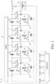
- FIG. 1 Shown in FIG. 1 is a charging system 10 comprising a sensor 12, a converter stage 14, a converter stage 16, a converter stage 18, a converter stage 20, a controller 22, a cell 24, a cell 26, a cell 28, a cell 30, a bus 31, and a charging unit 32.
- Converter stage 14 comprises a switch S41, a switch S42, a switch S43, a switch S44, a diode 50, an inductor 52, and a capacitor 54.
- Converter stage 16 comprises a switch S31, a switch S32, a switch S33, a switch S34, a diode 44, an inductor 46, and a capacitor 48.
- Converter stage 18 comprises a switch S21, a switch S22, a switch S23, a switch S24, a diode 38, an inductor 40, and a capacitor 42.
- Converter stage 20 comprises a switch S11, a switch S12, a switch S13, a switch S14, a diode 33, an inductor 34, and a capacitor 36.
- Cells 24, 26, 28, and 30 are four cells connected in series that are part of a larger battery. Each cell is an energy storage unit that can be recharged. Each cell could be made up of subcells.
- Each of converter stages 14, 16, 18, and 20 (14-20) are configurable into one of three configurations; source configuration, sink configuration, and non-sink, non-source (passive) configuration.
- the converter stage In the sink configuration, the converter stage provides charging current to the cell to which it corresponds. In the source configuration, the converter stage takes current from the cell to which it corresponds and provides that current to the converter stage that is in the sink configuration. A converter stage in the passive configuration neither sources current nor sinks current.
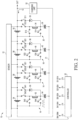
- Cell 24 has a negative terminal connected to a positive terminal of a cell not shown and a positive terminal.
- Cell 26 has a negative terminal connected to the positive terminal of cell 24 and a positive terminal.
- Cell 28 has a negative terminal connected to the positive terminal of cell 26 and a positive terminal.
- Cell 30 has a negative terminal connected to the positive terminal of cell 28 and a positive terminal providing an output OUT.
- Charging unit 32 has a first terminal connected to out and a second terminal connected to the negative terminal of the last cell (not shown).
- Sensor 12 has a first input coupled to the negative terminal of cell 24, a second input connected to a node connected to the negative terminal of cell 26 and the positive terminal of cell 24, a third input connected to node connected to the negative terminal of cell 28 and the positive terminal of cell 26, a fourth input connected to a node connected to the negative terminal of cell 30 and the positive terminal of cell 28, a fifth input connected to the positive terminal of cell 30, and an output connected to an input of controller 22.
- Controller 22 has a set of outputs for each converter unit that sets the configuration for the converter units by controlling the switches of each converter unit.
- Converter unit 14 receives a set of outputs for controlling switches S41, S42, S43, and S44.
- Converter unit 16 receives a set of outputs for controlling switches S31, S32, S33, and S34.
- Converter unit 18 receives a set of outputs for controlling switches S21, S22, S23, and S24.
- Converter unit 20 receives a set of outputs for controlling switches S11, S12, S13, and S14.
- switch S41 has a first terminal connected to the positive terminal of cell 24 and a second terminal connected to an anode of diode 50.
- Switch S42 has a first terminal connected to the positive terminal of cell 24 and a second terminal.
- Switch 43 has a first terminal connected to the negative terminal of cell 24 and a second terminal connected to a first terminal of inductor 52.
- Switch S44 has a first terminal connected to the negative terminal of cell 24 and a second terminal connected to a second terminal of inductor 52 and a cathode of diode 50.
- Capacitor 54 has a first terminal connected to the second terminal of inductor 52 and a second terminal connected to bus 31.
- Switch S31 has a first terminal connected to the positive terminal of cell 26 and a second terminal connected to an anode of diode 44.
- Switch S32 has a first terminal connected to the positive terminal of cell 26 and a second terminal.
- Switch S33 has a first terminal connected to the negative terminal of cell 26 and a second terminal connected to a first terminal of inductor 46.
- Switch S34 has a first terminal connected to the negative terminal of cell 26 and a second terminal connected to a second terminal of inductor 46 and a cathode of diode 44.
- Capacitor 48 has a first terminal connected to the second terminal of inductor 46 and a second terminal connected to bus 31.
- Switch S21 has a first terminal connected to the positive terminal of cell 28 and a second terminal connected to an anode of diode 38.
- Switch S22 has a first terminal connected to the positive terminal of cell 28 and a second terminal.
- Switch S23 has a first terminal connected to the negative terminal of cell 28 and a second terminal connected to a first terminal of inductor 40.
- Switch S24 has a first terminal connected to the negative terminal cell 28 and a second terminal connected to a second terminal of inductor 40 and a cathode of diode 38.
- Capacitor 42 has a first terminal connected to the second terminal of inductor 40 and a second terminal connected to bus 31.
- Switch S11 has a first terminal connected to the positive terminal of cell 30 and a second terminal connected to an anode of diode 33.
- Switch S12 has a first terminal connected to the positive terminal of cell 30 and a second terminal.
- Switch S13 has a first terminal connected to the negative terminal of cell 30 and a second terminal connected to a first terminal of inductor 34.
- Switch 14 has a first terminal connected to the negative terminal cell 30 and a second terminal connected to a second terminal of inductor 34 and a cathode of diode 32.
- Capacitor 36 has a first terminal connected to the second terminal of inductor 34 and a second terminal connected to bus 31.
- system 10 charges cells 24-30 via charging unit 32. Charging current flows from the positive terminal through the cell to the negative terminal of cells 24-30.
- sensor 12 senses the individual cell voltages or possibly other characteristics and provides that information to controller 22.
- Controller 22 responds by configuring the converter unit that corresponds to the cell with the highest voltage or highest state of charge to the source configuration and the converter unit that corresponds to the cell with the lowest voltage or lowest state of charge to the sink configuration.
- the other converter units are held in the passive configuration. While usually the cell chosen to be used as the source or sink has the absolute highest or lowest value respectively, the selection may be based on other criteria such as expected degradation or expected different loading.
- the effect of this balancing process is to reduce the net current charging the cell which is sourcing balancing power and to increase the net current charging the cell which is sinking power.
- Sensor 12 continues to monitor the voltage of the cells and couple that information to controller 22. Periodically or at such time as a different cell becomes the highest or lowest voltage, the corresponding converter unit is switched to the appropriate configuration and the cell that is no longer the highest or lowest has its converter unit switched to the passive configuration. This process of identifying the cell with the highest and lowest voltage and responding with the proper configuration for the corresponding converter units continues. At some point the charging unit will eventually stop providing current. Controller 22 may continue with the process even after charging unit 32 has stopped providing current in order to achieve an equal SoC for all of the cells.
- controller 22 may continue with the process while the cells are providing current to a load (not shown).
- the balancing process may be discontinued upon the termination of the charging from charging unit 32.
- all of the converter units are placed in the passive configuration if the cells are all satisfactorily balanced.
- all of converter units 24-30 are in the passive configuration which is the configuration in which all four switches are open. If only one cell is different, then in an arrangement not encompassed by the wording of the claims, any one of the other cells of equal voltage may be selected as the other converter unit of the pair. In such an arrangement, one convention for selecting the pair is to choose the one closest to the different one on the negative terminal, but other conventions may also be used.
- Converter unit 14 is placed in the source configuration and converter unit 20 is placed in the sink configuration. The other converter units remain in the passive configuration. Converter unit 14 is placed in the source configuration by closing switch S42 and switch S44 being switched between open and closed in response to a train of pulses.
- Closing switch S42 has the effect of coupling the first terminal of inductor 52 to the positive terminal of cell 24.
- the opening and closing of switch S44 has the effect of, responsive to the train of pulses, coupling and decoupling the negative terminal of cell 24 to the second terminal of inductor 52 and the first terminal of capacitor 54.
- Capacitor 54 is charged and discharged in a manner that drains current from cell 24 or at least preventing some of the charging current from reaching cell 24.
- Converter unit 20 is placed in the sink configuration by closing switches S11 and S13.
- the effect of closing switch S11 is to couple the anode of diode 33 to the positive terminal of cell 30.
- the effect of closing switch S13 is to couple the first terminal of inductor 34 to the negative terminal of cell 30.
- the switching on bus 31 has the effect of causing current to flow into cell 30 from the positive terminal to the negative terminal and thus increasing the charging of cell 30.
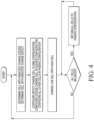
- FIG. 3 Shown in FIG. 3 is a method 60 that shows the operation of system 10.
- step 62 there is a determination of the cell with greatest charge excess and the cell with the greatest charge deficit. Usually, this will correspond to the highest and lowest voltage cells or highest and lowest state of charge cells respectively, but this is not required.
- step 64 the lowest charged cell has its converter unit configured in the sink configuration and the highest charged cell has its converter unit configured in the source configuration. As shown in step 66, this has the effect of charging the lowest charged cell with the highest charged cell.
- step 68 if there is a change in the highest charged cell, then the highest charged cell is changed to the passive configuration as shown in step 70 and the new highest charged cell is changed to the source configuration.
- step 74 if there is a change in the lowest charged cell, then the converter unit of the lowest charged cell is converted to the passive configuration as shown in step 75 and the new lowest charged cell has its converter unit changed to the sink configuration.
- step 77 if all of the cells are at the same voltage, all of the cells have their converter units changed to the passive configuration which may be the end as shown in step 79.
- the cells may be continually monitored so that step 62 may begin at any during this monitoring. The monitoring is not limited to the times that charging unit 32 is charging.
- Method 60 may also be used when the cells are providing output current OUT. This would have the effect of improving the balance of the voltage present on each cell. Shown in FIG. 4 is a flow chart showing less detail than shown in FIG. 3 and may aid understanding of method 60.
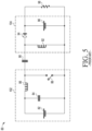
- Shown in FIG. 5 is a single-ended primary inductor converter (SEPIC) 80 driving a load 98 comprising a voltage supply 82, a capacitor 84, an inductor 86, a switch 88, a capacitance 90, an inductor 92, a diode 94, and a capacitor 96.
- Switch 88 is opened and closed responsive to a train of pulses.
- SEPIC 80 uses voltage supply 82 to provide a voltage across load 98 that may be greater than or less than the voltage of voltage supply 82.
- SEPIC 80 may be considered to have a source portion 102 and a sink portion 104 which are coupled via capacitance 90.
- Source portion 102 includes voltage supply 82, capacitor 84, inductor 86, and switch 88.
- Sink portion 104 includes inductor 92, diode 94, a capacitance 96. Sink portion 104 and source portion 102 are isolated by capacitance 90 and the voltage across load 98 can be higher, lower, or the same as the voltage of voltage supply 82.
- the output drive can be controlled by the duty cycle of the pulse train.
- SEPIC 80 is analogous to the operation of converter unit 14 and cell 24 in combination with converter unit 20 and cell 30 as shown in FIG. 2 with converter unit 14 in the source configuration and converter unit 20 in the sink configuration.
- cell 24 is analogous to voltage supply 82 and has capacitance analogous to capacitor 84
- inductor 52 is analogous to inductor 86.
- the analogous elements are connected in the same way.
- cell 30 has capacitance analogous to capacitance 96
- diode 33 is analogous to diode 94
- inductor 34 is analogous to inductor 92.
- the analogous elements are connected in the same way.
- the combination of capacitors 54 and 36, which are in series through bus 34, are analogous to capacitance 90 of SEPIC 80.
- the combination of converter unit 14 in the source configuration and converter unit 20 in the sink mode is a SEPIC.
- Each converter unit can be in the sink configuration or the source configuration and when a pair of converter units have that combination of one in the source configuration and one in the sink configuration, a SEPIC is the result.
- a SEPIC is thus particularly advantageous for this application.
- other types of converters may be able to be used in this manner of providing current to a lower SoC cell from a higher SoC cell directly and thus efficiently.
- the method includes determining a cell with the greatest charge excess of the plurality of battery cells.
- the method includes determining a cell with the greatest charge deficit of the plurality of battery cells.
- the method includes discharging the cell with the greatest charge excess to charge, with a voltage converter, the cell with the greatest charge deficit.
- the voltage converter is a SEPIC voltage converter.
- the method further comprises a plurality of converter stages, wherein each converter stage of the plurality is associated with a cell of the plurality of battery cells, wherein the discharging includes using a converter stage associated with the cell with the greatest charge excess as a source stage of the voltage converter and a converter stage associated with the cell with the greatest charge deficit as a sink stage of the voltage converter.
- the method may further comprise after the discharging, determining a second cell with the greatest charge deficit of the plurality of battery cells and discharging after the determining a second cell, the cell with the greatest charge excess to charge, with a voltage converter, the second cell, wherein the discharging after the determining a second cell includes using the converter stage associated with the cell with the greatest charge excess as a source stage of the voltage converter and a converter stage associated with the second cell as a sink stage of the voltage converter.
- the method may have a further characterization by which during the discharging the cell, the converter stage associated with the second cell is configured in a passive configuration; and during the discharging after the determining, the converter stage used as a sink stage for the discharging is configured in a passive configuration.
- the method may further comprise after the discharging, determining a second cell with the greatest charge excess of the plurality of battery cells and discharging after the determining a second cell, the second cell to charge, with a voltage converter, the cell with the greatest charge deficit, wherein the discharging after the determining a second cell includes using a converter stage of the second cell as a source stage of the voltage converter and the converter stage of the cell associated with the greatest charge deficit as the sink stage of the voltage converter.
- the method may further comprise after the discharging, performing a determining operation, wherein the performing includes determining a cell with the greatest charge deficit of the plurality of battery cells and determining a cell with the greatest charge excess of the plurality of battery cells and discharging the cell with the greatest charge excess as determined by the performing, to charge, with a voltage converter, the cell with the greatest charge deficit as determined by the performing.
- the method may have a further characterization by which the discharging occurs during a charging operation of the plurality of battery cells.
- the method may have a further characterization by which the discharging occurs during the plurality of battery cells providing power to a load.
- the circuit includes a bus.
- the circuit includes a plurality of converter stages each coupled to the bus, wherein each stage of the plurality of converter stages is associated with a cell of the plurality of battery cells, wherein each stage of the plurality of converter stages is configurable to serve as a source stage of a voltage converter for discharging the cell associated with the source stage to charge, via the bus, another cell of the plurality of battery cells, and wherein each stage of the plurality of converter stages is configurable to serve as a sink stage for a voltage converter for charging the cell of the plurality of battery cells associated with the sinkd stage from another cell of the plurality of battery cells via the bus.
- the circuit includes control circuitry for controlling the configuration of the plurality of converter stages.
- Each stage of the plurality of converter stages is configurable as a source stage for a single ended primary inductor converter (SEPIC) and each stage of the plurality of converter stages is configurable as a sink stage for a single ended primary inductor converter (SEPIC).
- SEPIC single ended primary inductor converter
- Each stage of the plurality of converter stages includes an inductor, a switch, and a capacitor. The capacitor of each stage of the plurality of converter stages is connected to the bus.
- the circuit may have a further characterization by which, when each converter stage is configured as a source stage of a voltage converter, a first terminal of the inductor of that converter stage is connected to a positive terminal of a cell associated with the each converter stage, wherein when the each converter stage is configured as a sink stage of a voltage converter, the first terminal of the inductor of that converter stage is connected to a negative terminal of the cell associated with the each converter stage.
- the circuit may have a further characterization by which, when each converter stage is configured in a passive configuration, the first terminal of the inductor is not connected to either the positive terminal or the negative terminal of the cell associated with each converter stage.
- the circuit may have a further characterization by which each stage of the plurality of converter stages comprises a switch having a first terminal connected to a second terminal of the inductor of each stage, the switch has a second terminal connected to the negative terminal of the cell associated with the each converter stage, wherein when the stage that is configured as a source stage of a voltage converter, the control circuitry provides a pulse width modulated signal to control the conductivity of the switch of the stage.
- the circuit may have a further characterization by which during an equalization operation, a controller configures a converter stage of the plurality of converter stages associated with a cell of the plurality of battery cells determined to have the greatest charge excess as a source stage of a voltage converter and configures a converter stage of the plurality of converter stages associated with a cell of the plurality of battery cells determined to have the greatest charge deficit as a sink stage of the voltage converter to provide charge for charging the cell determined to have the greatest charge deficit.
- the circuit may have a further characterization by which during an equalization operation, the controller configures no more than one converter stage of the plurality of converter stages as a source stage and no more than one converter stage of the plurality of converter stages as a sink stage.
- the circuit includes sensor circuitry for determining the state of charge of each cell of the plurality of battery cells.
- the circuit includes a first converter stage.
- the circuit includes a second converter stage, the second converter stage coupled to the first converter stage by at least one capacitor.
- the circuit includes control circuitry, wherein during a cell equalization operation, the control circuitry provides control signals to enable the first stage to be a source stage of a single ended primary inductor converter (SEPIC) converter and the second stage to be a sink stage for the SEPIC converter for discharging a first cell of the plurality of battery cells to transfer charge to a second cell of the plurality of battery cells to charge the second cell.
- SEPIC single ended primary inductor converter
- the circuit has a further characterization by which the first converter stage includes a first inductor and the second converter stage includes a second inductor, the first inductor and the second inductor are coupled by the at least one capacitor.
- switches may be preferably implemented using MOS transistors but other switches may be used. Accordingly, the specification and figures are to be regarded in an illustrative rather than a restrictive sense. Any benefits, advantages, or solutions to problems that are described herein with regard to specific embodiments are not intended to be construed as a critical, required, or essential feature or element of any or all the claims.
- Coupled is not intended to be limited to a direct coupling or a mechanical coupling.
Landscapes
- Engineering & Computer Science (AREA)
- Power Engineering (AREA)
- Charge And Discharge Circuits For Batteries Or The Like (AREA)
- Secondary Cells (AREA)
- Battery Mounting, Suspending (AREA)
Claims (8)
- Verfahren (60) zum Betreiben eines Batteriesystems, das mehrere Batteriezellen (24, 26, 28, 30), die in Reihe gekoppelt sind, und mehrere Wandlerstufen (14, 16, 18, 20) umfasst, wobei jede Stufe der mehreren Wandlerstufen einen Induktor (34, 40, 46, 52), einen Schalter (S14, S24, S34, S44) und einen Kondensator (36, 42, 48, 54) umfasst, und wobei die mehreren Batteriezellen mindestens drei Batteriezellen, die in Reihe gekoppelt sind, enthalten, und jede Zelle der mehreren Batteriezellen mit einer Wandlerstufe der mehreren Wandlerstufen assoziiert ist, wobei die Anzahl von Batteriezellen gleich der Anzahl von Wandlerstufen ist,wobei das Verfahren (60) umfasst:Bestimmen (62) einer Zelle (24) mit einem größten Ladungsüberschuss der mehreren Batteriezellen;Bestimmen (62) einer Zelle (30) mit einem größten Ladungsdefizit der mehreren Batteriezellen;Entladen der Zelle mit dem größten Ladungsüberschuss, um mit einem Spannungswandler die Zelle mit dem größten Ladungsdefizit zu laden (66), wobei das Entladen umfasst:Verwenden einer Wandlerstufe, die mit der Zelle (24) mit dem größten Ladungsüberschuss assoziiert ist, als eine Quellstufe des Spannungswandlers, undVerwenden einer Wandlerstufe, die mit der Zelle (30) mit dem größten Ladungsdefizit assoziiert ist, als eine Senkenstufe des Spannungswandlers;wobei das Verwenden einer Wandlerstufe, die mit der Zelle (24) mit dem größten Ladungsüberschuss assoziiert ist, als eine Quellstufe des Spannungswandlers, und Verwenden einer Wandlerstufe, die mit der Zelle (30) mit dem größten Ladungsdefizit assoziiert ist, als eine Senkenstufe des Spannungswandlers, das Auslegen des Spannungswandlers als einen SEPIC (Single-Ended Primary Inductor Converter) umfasst.
- Verfahren (60) nach Anspruch 1, weiter umfassend:nach dem Entladen das Bestimmen einer zweiten Zelle mit dem größten Ladungsdefizit der mehreren Batteriezellen (74); undnach dem Bestimmen der zweiten Zelle das Entladen der Zelle (24) mit dem größten Ladungsüberschuss, um mit einem Spannungswandler die zweite Zelle zu laden, wobei das Entladen nach dem Bestimmen der zweiten Zelle (66) umfasst:Verwenden der Wandlerstufe, die mit der Zelle (24) mit dem größten Ladungsüberschuss assoziiert ist, als eine Quellstufe des Spannungswandlers, undVerwenden einer Wandlerstufe, die mit der zweite Zelle assoziiert ist, als eine Senkenstufe des Spannungswandlers.
- Verfahren (60) nach Anspruch 2, weiter umfassend:während des Entladens der Zelle das Auslegen der Wandlerstufe, die mit der zweiten Zelle assoziiert ist, in einer passiven Konfiguration; undwährend des Entladens nach dem Bestimmen der zweiten Zelle, das Auslegen der Wandlerstufe, die als eine Senkenstufe für das Entladen der Zelle verwendet wird, in einer passiven Konfiguration.
- Schaltung, die ausgelegt ist zum Steuern eines Betriebs von mehreren Batteriezellen, die in Reihe gekoppelt sind (24, 26, 28, 30), wobei die mehreren Batteriezellen mindestens drei Zellen enthalten, wobei die Schaltung umfasst:eine Sensorschaltungsanordnung (12), die ausgelegt ist zum Bestimmen eines Ladezustands jeder Zelle der mehreren Batteriezellen (12), wobei die Sensorschaltungsanordnung (12) ausgelegt ist zum Bestimmen einer Zelle mit einem größten Ladungsüberschuss der mehreren Batteriezellen (62) und zum Bestimmen einer Zelle mit einem größten Ladungsdefizit der mehreren Batteriezellen (62);einen Bus (31);mehrere Wandlerstufen (14, 16, 18, 20), die jeweils an den Bus gekoppelt sind, wobeijede Zelle der mehreren Batteriezellen mit einer Wandlerstufe der mehreren Wandlerstufen (14, 16, 18, 20) assoziiert ist, wobei die Anzahl von Batteriezellen gleich der Anzahl von Wandlerstufen ist,jede Stufe der mehreren Wandlerstufen einen Induktor (34, 40, 46, 52), einen Schalter (S14, S24, S34, S44) und einen Kondensator (36, 42, 48, 54) umfasst,der Kondensator jeder Stufe der mehreren Wandlerstufen an den Bus (31) angeschlossen ist,jede Stufe der mehreren Wandlerstufen ausgelegt werden kann zum Dienen als eine Quellstufe eines Spannungswandlers zum Entladen der Zelle, die mit der Quellenstufe assoziiert ist, um über den Bus (31) eine andere Zelle der mehreren Batteriezellen zu laden, undjede Stufe der mehreren Wandlerstufen ausgelegt werden kann zum Dienen als eine Senkenstufe für einen Spannungswandler zum Laden der Zelle der mehreren Batteriezellen, die mit der Senkenstufe assoziiert ist, von einer anderen Zelle der mehreren Batteriezellen über den Bus (31); undeine Steuerschaltungsanordnung (22), die mit der Sensorschaltungsanordnung (12) verbunden ist und ausgelegt ist zum Steuern der Konfiguration der mehreren Wandlerstufen, wobei die Steuerschaltungsanordnung (22) angepasst ist zum Auslegen eines Spannungswandlers als einen SEPIC (Single-Ended Primary Inductor Converter) durch:Verwenden einer Wandlerstufe, die mit einer Zelle (24) mit dem größten Ladungsüberschuss assoziiert ist, als eine Quellenstufe des Spannungswandlers, undVerwenden einer Wandlerstufe, die mit der Zelle (30) mit dem größten Ladungsdefizit assoziiert ist, als eine Senkenstufe des Spannungswandlers.
- Schaltung nach Anspruch 4, wobeiwenn jede Wandlerstufe als eine Quellenstufe eines Spannungswandlers ausgelegt ist, ein erster Anschluss des Induktors (34, 40, 46, 52) mit einem positiven Anschluss einer Zelle verbunden ist, die mit jeder Wandlerstufe assoziiert ist, undwenn jede Wandlerstufe als eine Senkenstufe eines Spannungswandlers ausgelegt ist, der erste Anschluss des Induktors (34,40, 46, 52) mit einem negativen Anschluss der Zelle verbunden ist, die mit jeder Wandlerstufe assoziiert ist.
- Schaltung nach Anspruch 5, wobei, wenn jede Wandlerstufe in einer passiven Konfiguration ausgelegt ist, der erste Anschluss des Induktors (34, 40, 46, 52) nicht mit entweder dem positiven Anschluss oder dem negativen Anschluss der Zelle verbunden ist, die mit jeder Wandlerstufe verbunden ist.
- Schaltung nach Anspruch 5, wobei
der Schalter jeder Stufe der mehreren Wandlerstufen (S14, S24, S34, S44) einen ersten Anschluss aufweist, der mit einem zweiten Anschluss des Induktors jeder Stufe verbunden ist, wobei der Schalter einen zweiten Anschluss aufweist, der mit dem negativen Anschluss der Zelle verbunden ist, die mit jeder Wandlerstufe assoziiert ist, und die Steuerschaltungsanordnung ausgelegt ist zum, wenn eine Stufe als ein Quellenstufe eines Spannungswandlers ausgelegt ist, Liefern eines pulsbreitenmodulierten Signals, um die Leitfähigkeit des Schalters der Stufe zu steuern. - Schaltung nach Anspruch 4, wobei die Steuerschaltungsanordnung (22) ausgelegt ist, um, während eines Ausgleichsbetriebs, nicht mehr als eine Wandlerstufe der mehreren Wandlerstufen als eine Quellenstufe auszulegen und nicht mehr als eine Wandlerstufe der mehreren Wandlerstufen als eine Senkenstufe auszulegen.
Applications Claiming Priority (1)
| Application Number | Priority Date | Filing Date | Title |
|---|---|---|---|
| US12/833,430 US8436582B2 (en) | 2010-07-09 | 2010-07-09 | Battery cell equalizer system |
Publications (3)
| Publication Number | Publication Date |
|---|---|
| EP2405554A2 EP2405554A2 (de) | 2012-01-11 |
| EP2405554A3 EP2405554A3 (de) | 2014-07-30 |
| EP2405554B1 true EP2405554B1 (de) | 2023-08-09 |
Family
ID=44744768
Family Applications (1)
| Application Number | Title | Priority Date | Filing Date |
|---|---|---|---|
| EP11170004.3A Active EP2405554B1 (de) | 2010-07-09 | 2011-06-15 | Ladezustandsausgleichssystem für Batteriezellen |
Country Status (4)
| Country | Link |
|---|---|
| US (1) | US8436582B2 (de) |
| EP (1) | EP2405554B1 (de) |
| JP (1) | JP2012019685A (de) |
| CN (1) | CN102315671B (de) |
Families Citing this family (47)
| Publication number | Priority date | Publication date | Assignee | Title |
|---|---|---|---|---|
| US8473250B2 (en) | 2006-12-06 | 2013-06-25 | Solaredge, Ltd. | Monitoring of distributed power harvesting systems using DC power sources |
| US9088178B2 (en) | 2006-12-06 | 2015-07-21 | Solaredge Technologies Ltd | Distributed power harvesting systems using DC power sources |
| US8947194B2 (en) | 2009-05-26 | 2015-02-03 | Solaredge Technologies Ltd. | Theft detection and prevention in a power generation system |
| US11569659B2 (en) | 2006-12-06 | 2023-01-31 | Solaredge Technologies Ltd. | Distributed power harvesting systems using DC power sources |
| US8963369B2 (en) | 2007-12-04 | 2015-02-24 | Solaredge Technologies Ltd. | Distributed power harvesting systems using DC power sources |
| US11687112B2 (en) | 2006-12-06 | 2023-06-27 | Solaredge Technologies Ltd. | Distributed power harvesting systems using DC power sources |
| US11309832B2 (en) | 2006-12-06 | 2022-04-19 | Solaredge Technologies Ltd. | Distributed power harvesting systems using DC power sources |
| US8319471B2 (en) | 2006-12-06 | 2012-11-27 | Solaredge, Ltd. | Battery power delivery module |
| US11888387B2 (en) | 2006-12-06 | 2024-01-30 | Solaredge Technologies Ltd. | Safety mechanisms, wake up and shutdown methods in distributed power installations |
| US12316274B2 (en) | 2006-12-06 | 2025-05-27 | Solaredge Technologies Ltd. | Pairing of components in a direct current distributed power generation system |
| US8816535B2 (en) | 2007-10-10 | 2014-08-26 | Solaredge Technologies, Ltd. | System and method for protection during inverter shutdown in distributed power installations |
| US8013472B2 (en) | 2006-12-06 | 2011-09-06 | Solaredge, Ltd. | Method for distributed power harvesting using DC power sources |
| US11735910B2 (en) | 2006-12-06 | 2023-08-22 | Solaredge Technologies Ltd. | Distributed power system using direct current power sources |
| US8319483B2 (en) | 2007-08-06 | 2012-11-27 | Solaredge Technologies Ltd. | Digital average input current control in power converter |
| US11855231B2 (en) | 2006-12-06 | 2023-12-26 | Solaredge Technologies Ltd. | Distributed power harvesting systems using DC power sources |
| US8618692B2 (en) | 2007-12-04 | 2013-12-31 | Solaredge Technologies Ltd. | Distributed power system using direct current power sources |
| CN101933209B (zh) | 2007-12-05 | 2015-10-21 | 太阳能安吉有限公司 | 分布式电力装置中的安全机构、醒来和关闭方法 |
| EP2294669B8 (de) | 2008-05-05 | 2016-12-07 | Solaredge Technologies Ltd. | Gleichstrom-leistungskombinierer |
| US12418177B2 (en) | 2009-10-24 | 2025-09-16 | Solaredge Technologies Ltd. | Distributed power system using direct current power sources |
| US9490639B2 (en) * | 2010-02-05 | 2016-11-08 | Commissariat A L'energie Atomique Et Aux Energies Alternatives | Charge equalization system for batteries |
| GB2485527B (en) | 2010-11-09 | 2012-12-19 | Solaredge Technologies Ltd | Arc detection and prevention in a power generation system |
| US10673229B2 (en) | 2010-11-09 | 2020-06-02 | Solaredge Technologies Ltd. | Arc detection and prevention in a power generation system |
| GB2483317B (en) | 2011-01-12 | 2012-08-22 | Solaredge Technologies Ltd | Serially connected inverters |
| US9099870B2 (en) * | 2011-06-11 | 2015-08-04 | Sendyne Corporation | Charge redistribution method for cell arrays |
| EP2549619A1 (de) * | 2011-07-19 | 2013-01-23 | Kabushiki Kaisha Toyota Jidoshokki | Lade- und Abladesteuervorrichtung |
| WO2013031394A1 (ja) * | 2011-09-02 | 2013-03-07 | 日本電気株式会社 | 電池制御システム、電池制御装置、電池制御方法、および記録媒体 |
| GB2498365A (en) | 2012-01-11 | 2013-07-17 | Solaredge Technologies Ltd | Photovoltaic module |
| US9853565B2 (en) | 2012-01-30 | 2017-12-26 | Solaredge Technologies Ltd. | Maximized power in a photovoltaic distributed power system |
| GB2498790A (en) | 2012-01-30 | 2013-07-31 | Solaredge Technologies Ltd | Maximising power in a photovoltaic distributed power system |
| GB2498791A (en) | 2012-01-30 | 2013-07-31 | Solaredge Technologies Ltd | Photovoltaic panel circuitry |
| CN103368268B (zh) * | 2012-03-27 | 2015-04-15 | 无锡富洪科技有限公司 | 串联储能元件组的电压主动均衡系统及方法 |
| KR101326103B1 (ko) * | 2012-03-29 | 2013-11-06 | 숭실대학교산학협력단 | 배터리 충전량 밸런싱 장치 및 배터리 충전량 밸런싱 시스템 |
| US9583957B2 (en) * | 2012-09-10 | 2017-02-28 | Silicon Works Co., Ltd. | Cell balancing integrated circuit, cell balancing system, and cell balancing method |
| KR101450717B1 (ko) * | 2013-01-18 | 2014-10-16 | 포항공과대학교 산학협력단 | 엘씨 직렬공진을 이용한 배터리셀 밸런싱 회로 |
| US9548619B2 (en) * | 2013-03-14 | 2017-01-17 | Solaredge Technologies Ltd. | Method and apparatus for storing and depleting energy |
| KR101451009B1 (ko) * | 2013-03-27 | 2014-10-15 | 주식회사 엘지씨엔에스 | 직렬 연결된 다수 개의 전지 직류 마이크로그리드 충방전 시스템 |
| JP5975169B2 (ja) * | 2013-03-29 | 2016-08-23 | 日本電気株式会社 | 充放電装置、充放電制御方法、及びプログラム |
| US9203246B2 (en) * | 2013-05-16 | 2015-12-01 | Postech Academy-Industry Foundation | Balancing control circuit for battery cell module using LC series resonant circuit |
| EP2916424B1 (de) * | 2014-03-04 | 2018-05-30 | Ricoh Company, Ltd. | Speicherausgleichsschaltung, Speicherausgleichsvorrichtung, Speicherbatteriepack und Schaltkreissteuerungsverfahren |
| CN105449734A (zh) * | 2015-06-02 | 2016-03-30 | 武汉众宇动力系统科技有限公司 | 电池均衡装置及其充放电均衡方法 |
| KR101917913B1 (ko) | 2015-07-23 | 2018-11-12 | 주식회사 엘지화학 | 배터리 스택 밸런싱 장치 |
| US11018623B2 (en) | 2016-04-05 | 2021-05-25 | Solaredge Technologies Ltd. | Safety switch for photovoltaic systems |
| US12057807B2 (en) | 2016-04-05 | 2024-08-06 | Solaredge Technologies Ltd. | Chain of power devices |
| US11177663B2 (en) | 2016-04-05 | 2021-11-16 | Solaredge Technologies Ltd. | Chain of power devices |
| US11251628B2 (en) * | 2017-01-23 | 2022-02-15 | Rafael Advanced Defense Systems Ltd. | System for balancing a series of cells |
| CN107171416B (zh) * | 2017-07-25 | 2023-07-07 | 贵州大学 | 一种新型的均衡电路及其控制方法 |
| CN113708466B (zh) * | 2021-10-25 | 2022-03-11 | 广东希荻微电子股份有限公司 | 一种电池充放电电路和终端设备 |
Family Cites Families (15)
| Publication number | Priority date | Publication date | Assignee | Title |
|---|---|---|---|---|
| US5659237A (en) * | 1995-09-28 | 1997-08-19 | Wisconsin Alumni Research Foundation | Battery charging using a transformer with a single primary winding and plural secondary windings |
| JP3922655B2 (ja) * | 1996-07-12 | 2007-05-30 | 株式会社東京アールアンドデー | 電源装置の制御システムおよび電源装置の制御方法 |
| US5869950A (en) * | 1997-10-30 | 1999-02-09 | Lockheed Martin Corp. | Method for equalizing the voltage of traction battery modules of a hybrid electric vehicle |
| FR2776139B1 (fr) * | 1998-03-13 | 2002-03-08 | Denso Corp | Dispositif d'equilibrage des tensions dans une batterie composee |
| US6373223B1 (en) * | 2000-11-21 | 2002-04-16 | Nagano Japan Radio Co., Ltd. | Voltage equalizing apparatus and voltage equalizing method for battery devices |
| JP3630303B2 (ja) * | 2000-11-21 | 2005-03-16 | 長野日本無線株式会社 | 蓄電素子の電圧均等化装置 |
| TW571452B (en) * | 2002-12-13 | 2004-01-11 | Quanta Comp Inc | Charging-type electrical potential balance device |
| JP3795499B2 (ja) * | 2003-12-26 | 2006-07-12 | 富士重工業株式会社 | 蓄電素子の電圧均等化装置 |
| KR100666817B1 (ko) * | 2005-01-14 | 2007-01-09 | 주식회사 엘지화학 | 배터리의 밸런싱 장치 및 방법 |
| JP2006246645A (ja) * | 2005-03-04 | 2006-09-14 | Yazaki Corp | 均等化方法及びその装置 |
| US7592775B2 (en) * | 2006-05-31 | 2009-09-22 | Aeroflex Plainview, Inc. | Battery balancing including resonant frequency compensation |
| KR101124800B1 (ko) * | 2007-02-09 | 2012-03-23 | 한국과학기술원 | 전하 균일 장치 |
| US8575896B2 (en) * | 2008-02-15 | 2013-11-05 | Apple Inc. | Parallel battery architecture with shared bidirectional converter |
| US8203320B2 (en) * | 2009-01-07 | 2012-06-19 | Linear Technology Corporation | Switching mode converters |
| CN201438493U (zh) * | 2009-05-31 | 2010-04-14 | 比亚迪股份有限公司 | 车载动力电池组的均衡装置 |
-
2010
- 2010-07-09 US US12/833,430 patent/US8436582B2/en not_active Expired - Fee Related
-
2011
- 2011-06-15 EP EP11170004.3A patent/EP2405554B1/de active Active
- 2011-07-08 CN CN201110190190.4A patent/CN102315671B/zh active Active
- 2011-07-08 JP JP2011151482A patent/JP2012019685A/ja active Pending
Also Published As
| Publication number | Publication date |
|---|---|
| JP2012019685A (ja) | 2012-01-26 |
| CN102315671B (zh) | 2015-09-23 |
| US8436582B2 (en) | 2013-05-07 |
| EP2405554A2 (de) | 2012-01-11 |
| CN102315671A (zh) | 2012-01-11 |
| EP2405554A3 (de) | 2014-07-30 |
| US20120007558A1 (en) | 2012-01-12 |
Similar Documents
| Publication | Publication Date | Title |
|---|---|---|
| EP2405554B1 (de) | Ladezustandsausgleichssystem für Batteriezellen | |
| US8493028B2 (en) | Power management circuit for rechargeable battery stack | |
| US7804276B2 (en) | Circuit arrangement and method for transferring electrical charge between accumulators of an accumulator arrangement including a series circuit of accumulators | |
| CN101849340B (zh) | 集成有电压传感器和充电均衡器的电池管理系统 | |
| US9263887B2 (en) | Battery system and method for providing an intermediate voltage | |
| EP2302757B1 (de) | Verfahren und System zum Ladungsausgleich von elektrischen Energiespeicherzellen | |
| CN102655339B (zh) | 电源系统 | |
| US20130038289A1 (en) | Battery-cell converter systems | |
| US8970162B2 (en) | System and method for balancing electrical energy storage devices via differential power bus and capacitive load switched-mode power supply | |
| JP2013520947A (ja) | バッテリセルコンバータ管理システム | |
| US9225191B2 (en) | Circuit and method for voltage equalization in large batteries | |
| JP4691064B2 (ja) | 組電池の残容量均等化装置 | |
| US9048670B2 (en) | System and method for balancing electrical energy storage devices via differential power bus and capacitive load switched-mode power supply | |
| WO2020022344A1 (ja) | 電源システム、及び管理装置 | |
| EP2693595B1 (de) | Balancekorrekturvorrichtung und elektrisches speichersystem | |
| JP2011101572A (ja) | セルバランス機能を備えた充電システム | |
| US20150069960A1 (en) | Auxiliary Battery Charging Apparatus | |
| CN105873793A (zh) | 电化学能量存储器和用于平衡的方法 | |
| JP4696212B2 (ja) | キャパシタ電源システム | |
| US9166431B2 (en) | Battery charge circuit | |
| CN102738853A (zh) | 辅助电池充电装置 | |
| KR101816823B1 (ko) | 배터리 전하 균일 회로 | |
| JP5781415B2 (ja) | 車両用電源装置 | |
| RU153793U1 (ru) | Система управления аккумуляторной батареей | |
| JP2011004516A (ja) | 電源供給回路 |
Legal Events
| Date | Code | Title | Description |
|---|---|---|---|
| AK | Designated contracting states |
Kind code of ref document: A2 Designated state(s): AL AT BE BG CH CY CZ DE DK EE ES FI FR GB GR HR HU IE IS IT LI LT LU LV MC MK MT NL NO PL PT RO RS SE SI SK SM TR |
|
| AX | Request for extension of the european patent |
Extension state: BA ME |
|
| PUAI | Public reference made under article 153(3) epc to a published international application that has entered the european phase |
Free format text: ORIGINAL CODE: 0009012 |
|
| PUAL | Search report despatched |
Free format text: ORIGINAL CODE: 0009013 |
|
| AK | Designated contracting states |
Kind code of ref document: A3 Designated state(s): AL AT BE BG CH CY CZ DE DK EE ES FI FR GB GR HR HU IE IS IT LI LT LU LV MC MK MT NL NO PL PT RO RS SE SI SK SM TR |
|
| AX | Request for extension of the european patent |
Extension state: BA ME |
|
| RIC1 | Information provided on ipc code assigned before grant |
Ipc: H02J 7/00 20060101AFI20140623BHEP Ipc: H02M 3/158 20060101ALI20140623BHEP |
|
| 17P | Request for examination filed |
Effective date: 20150130 |
|
| RBV | Designated contracting states (corrected) |
Designated state(s): AL AT BE BG CH CY CZ DE DK EE ES FI FR GB GR HR HU IE IS IT LI LT LU LV MC MK MT NL NO PL PT RO RS SE SI SK SM TR |
|
| RAP1 | Party data changed (applicant data changed or rights of an application transferred) |
Owner name: NXP USA, INC. |
|
| STAA | Information on the status of an ep patent application or granted ep patent |
Free format text: STATUS: EXAMINATION IS IN PROGRESS |
|
| 17Q | First examination report despatched |
Effective date: 20210309 |
|
| GRAP | Despatch of communication of intention to grant a patent |
Free format text: ORIGINAL CODE: EPIDOSNIGR1 |
|
| STAA | Information on the status of an ep patent application or granted ep patent |
Free format text: STATUS: GRANT OF PATENT IS INTENDED |
|
| INTG | Intention to grant announced |
Effective date: 20230502 |
|
| GRAS | Grant fee paid |
Free format text: ORIGINAL CODE: EPIDOSNIGR3 |
|
| GRAA | (expected) grant |
Free format text: ORIGINAL CODE: 0009210 |
|
| STAA | Information on the status of an ep patent application or granted ep patent |
Free format text: STATUS: THE PATENT HAS BEEN GRANTED |
|
| AK | Designated contracting states |
Kind code of ref document: B1 Designated state(s): AL AT BE BG CH CY CZ DE DK EE ES FI FR GB GR HR HU IE IS IT LI LT LU LV MC MK MT NL NO PL PT RO RS SE SI SK SM TR |
|
| REG | Reference to a national code |
Ref country code: GB Ref legal event code: FG4D |
|
| REG | Reference to a national code |
Ref country code: CH Ref legal event code: EP |
|
| REG | Reference to a national code |
Ref country code: IE Ref legal event code: FG4D |
|
| REG | Reference to a national code |
Ref country code: DE Ref legal event code: R096 Ref document number: 602011074141 Country of ref document: DE |
|
| P01 | Opt-out of the competence of the unified patent court (upc) registered |
Effective date: 20230907 |
|
| REG | Reference to a national code |
Ref country code: LT Ref legal event code: MG9D |
|
| REG | Reference to a national code |
Ref country code: NL Ref legal event code: MP Effective date: 20230809 |
|
| REG | Reference to a national code |
Ref country code: AT Ref legal event code: MK05 Ref document number: 1598631 Country of ref document: AT Kind code of ref document: T Effective date: 20230809 |
|
| PG25 | Lapsed in a contracting state [announced via postgrant information from national office to epo] |
Ref country code: GR Free format text: LAPSE BECAUSE OF FAILURE TO SUBMIT A TRANSLATION OF THE DESCRIPTION OR TO PAY THE FEE WITHIN THE PRESCRIBED TIME-LIMIT Effective date: 20231110 |
|
| PG25 | Lapsed in a contracting state [announced via postgrant information from national office to epo] |
Ref country code: IS Free format text: LAPSE BECAUSE OF FAILURE TO SUBMIT A TRANSLATION OF THE DESCRIPTION OR TO PAY THE FEE WITHIN THE PRESCRIBED TIME-LIMIT Effective date: 20231209 |
|
| PG25 | Lapsed in a contracting state [announced via postgrant information from national office to epo] |
Ref country code: SE Free format text: LAPSE BECAUSE OF FAILURE TO SUBMIT A TRANSLATION OF THE DESCRIPTION OR TO PAY THE FEE WITHIN THE PRESCRIBED TIME-LIMIT Effective date: 20230809 Ref country code: RS Free format text: LAPSE BECAUSE OF FAILURE TO SUBMIT A TRANSLATION OF THE DESCRIPTION OR TO PAY THE FEE WITHIN THE PRESCRIBED TIME-LIMIT Effective date: 20230809 Ref country code: PT Free format text: LAPSE BECAUSE OF FAILURE TO SUBMIT A TRANSLATION OF THE DESCRIPTION OR TO PAY THE FEE WITHIN THE PRESCRIBED TIME-LIMIT Effective date: 20231211 Ref country code: NO Free format text: LAPSE BECAUSE OF FAILURE TO SUBMIT A TRANSLATION OF THE DESCRIPTION OR TO PAY THE FEE WITHIN THE PRESCRIBED TIME-LIMIT Effective date: 20231109 Ref country code: NL Free format text: LAPSE BECAUSE OF FAILURE TO SUBMIT A TRANSLATION OF THE DESCRIPTION OR TO PAY THE FEE WITHIN THE PRESCRIBED TIME-LIMIT Effective date: 20230809 Ref country code: LV Free format text: LAPSE BECAUSE OF FAILURE TO SUBMIT A TRANSLATION OF THE DESCRIPTION OR TO PAY THE FEE WITHIN THE PRESCRIBED TIME-LIMIT Effective date: 20230809 Ref country code: LT Free format text: LAPSE BECAUSE OF FAILURE TO SUBMIT A TRANSLATION OF THE DESCRIPTION OR TO PAY THE FEE WITHIN THE PRESCRIBED TIME-LIMIT Effective date: 20230809 Ref country code: IS Free format text: LAPSE BECAUSE OF FAILURE TO SUBMIT A TRANSLATION OF THE DESCRIPTION OR TO PAY THE FEE WITHIN THE PRESCRIBED TIME-LIMIT Effective date: 20231209 Ref country code: HR Free format text: LAPSE BECAUSE OF FAILURE TO SUBMIT A TRANSLATION OF THE DESCRIPTION OR TO PAY THE FEE WITHIN THE PRESCRIBED TIME-LIMIT Effective date: 20230809 Ref country code: GR Free format text: LAPSE BECAUSE OF FAILURE TO SUBMIT A TRANSLATION OF THE DESCRIPTION OR TO PAY THE FEE WITHIN THE PRESCRIBED TIME-LIMIT Effective date: 20231110 Ref country code: FI Free format text: LAPSE BECAUSE OF FAILURE TO SUBMIT A TRANSLATION OF THE DESCRIPTION OR TO PAY THE FEE WITHIN THE PRESCRIBED TIME-LIMIT Effective date: 20230809 Ref country code: AT Free format text: LAPSE BECAUSE OF FAILURE TO SUBMIT A TRANSLATION OF THE DESCRIPTION OR TO PAY THE FEE WITHIN THE PRESCRIBED TIME-LIMIT Effective date: 20230809 |
|
| PG25 | Lapsed in a contracting state [announced via postgrant information from national office to epo] |
Ref country code: PL Free format text: LAPSE BECAUSE OF FAILURE TO SUBMIT A TRANSLATION OF THE DESCRIPTION OR TO PAY THE FEE WITHIN THE PRESCRIBED TIME-LIMIT Effective date: 20230809 |
|
| PG25 | Lapsed in a contracting state [announced via postgrant information from national office to epo] |
Ref country code: ES Free format text: LAPSE BECAUSE OF FAILURE TO SUBMIT A TRANSLATION OF THE DESCRIPTION OR TO PAY THE FEE WITHIN THE PRESCRIBED TIME-LIMIT Effective date: 20230809 |
|
| PG25 | Lapsed in a contracting state [announced via postgrant information from national office to epo] |
Ref country code: SM Free format text: LAPSE BECAUSE OF FAILURE TO SUBMIT A TRANSLATION OF THE DESCRIPTION OR TO PAY THE FEE WITHIN THE PRESCRIBED TIME-LIMIT Effective date: 20230809 Ref country code: RO Free format text: LAPSE BECAUSE OF FAILURE TO SUBMIT A TRANSLATION OF THE DESCRIPTION OR TO PAY THE FEE WITHIN THE PRESCRIBED TIME-LIMIT Effective date: 20230809 Ref country code: ES Free format text: LAPSE BECAUSE OF FAILURE TO SUBMIT A TRANSLATION OF THE DESCRIPTION OR TO PAY THE FEE WITHIN THE PRESCRIBED TIME-LIMIT Effective date: 20230809 Ref country code: EE Free format text: LAPSE BECAUSE OF FAILURE TO SUBMIT A TRANSLATION OF THE DESCRIPTION OR TO PAY THE FEE WITHIN THE PRESCRIBED TIME-LIMIT Effective date: 20230809 Ref country code: DK Free format text: LAPSE BECAUSE OF FAILURE TO SUBMIT A TRANSLATION OF THE DESCRIPTION OR TO PAY THE FEE WITHIN THE PRESCRIBED TIME-LIMIT Effective date: 20230809 Ref country code: CZ Free format text: LAPSE BECAUSE OF FAILURE TO SUBMIT A TRANSLATION OF THE DESCRIPTION OR TO PAY THE FEE WITHIN THE PRESCRIBED TIME-LIMIT Effective date: 20230809 Ref country code: SK Free format text: LAPSE BECAUSE OF FAILURE TO SUBMIT A TRANSLATION OF THE DESCRIPTION OR TO PAY THE FEE WITHIN THE PRESCRIBED TIME-LIMIT Effective date: 20230809 |
|
| REG | Reference to a national code |
Ref country code: DE Ref legal event code: R097 Ref document number: 602011074141 Country of ref document: DE |
|
| PG25 | Lapsed in a contracting state [announced via postgrant information from national office to epo] |
Ref country code: IT Free format text: LAPSE BECAUSE OF FAILURE TO SUBMIT A TRANSLATION OF THE DESCRIPTION OR TO PAY THE FEE WITHIN THE PRESCRIBED TIME-LIMIT Effective date: 20230809 |
|
| PLBE | No opposition filed within time limit |
Free format text: ORIGINAL CODE: 0009261 |
|
| STAA | Information on the status of an ep patent application or granted ep patent |
Free format text: STATUS: NO OPPOSITION FILED WITHIN TIME LIMIT |
|
| PGFP | Annual fee paid to national office [announced via postgrant information from national office to epo] |
Ref country code: GB Payment date: 20240521 Year of fee payment: 14 |
|
| PGFP | Annual fee paid to national office [announced via postgrant information from national office to epo] |
Ref country code: DE Payment date: 20240521 Year of fee payment: 14 |
|
| 26N | No opposition filed |
Effective date: 20240513 |
|
| PG25 | Lapsed in a contracting state [announced via postgrant information from national office to epo] |
Ref country code: SI Free format text: LAPSE BECAUSE OF FAILURE TO SUBMIT A TRANSLATION OF THE DESCRIPTION OR TO PAY THE FEE WITHIN THE PRESCRIBED TIME-LIMIT Effective date: 20230809 |
|
| PGFP | Annual fee paid to national office [announced via postgrant information from national office to epo] |
Ref country code: FR Payment date: 20240522 Year of fee payment: 14 |
|
| PG25 | Lapsed in a contracting state [announced via postgrant information from national office to epo] |
Ref country code: BG Free format text: LAPSE BECAUSE OF FAILURE TO SUBMIT A TRANSLATION OF THE DESCRIPTION OR TO PAY THE FEE WITHIN THE PRESCRIBED TIME-LIMIT Effective date: 20230809 |
|
| PG25 | Lapsed in a contracting state [announced via postgrant information from national office to epo] |
Ref country code: BG Free format text: LAPSE BECAUSE OF FAILURE TO SUBMIT A TRANSLATION OF THE DESCRIPTION OR TO PAY THE FEE WITHIN THE PRESCRIBED TIME-LIMIT Effective date: 20230809 |
|
| PG25 | Lapsed in a contracting state [announced via postgrant information from national office to epo] |
Ref country code: MC Free format text: LAPSE BECAUSE OF FAILURE TO SUBMIT A TRANSLATION OF THE DESCRIPTION OR TO PAY THE FEE WITHIN THE PRESCRIBED TIME-LIMIT Effective date: 20230809 |
|
| REG | Reference to a national code |
Ref country code: CH Ref legal event code: PL |
|
| PG25 | Lapsed in a contracting state [announced via postgrant information from national office to epo] |
Ref country code: LU Free format text: LAPSE BECAUSE OF NON-PAYMENT OF DUE FEES Effective date: 20240615 |
|
| PG25 | Lapsed in a contracting state [announced via postgrant information from national office to epo] |
Ref country code: IE Free format text: LAPSE BECAUSE OF NON-PAYMENT OF DUE FEES Effective date: 20240615 |
|
| PG25 | Lapsed in a contracting state [announced via postgrant information from national office to epo] |
Ref country code: CH Free format text: LAPSE BECAUSE OF NON-PAYMENT OF DUE FEES Effective date: 20240630 Ref country code: BE Free format text: LAPSE BECAUSE OF NON-PAYMENT OF DUE FEES Effective date: 20240630 |
|
| REG | Reference to a national code |
Ref country code: BE Ref legal event code: MM Effective date: 20240630 |
|
| PG25 | Lapsed in a contracting state [announced via postgrant information from national office to epo] |
Ref country code: CY Free format text: LAPSE BECAUSE OF FAILURE TO SUBMIT A TRANSLATION OF THE DESCRIPTION OR TO PAY THE FEE WITHIN THE PRESCRIBED TIME-LIMIT; INVALID AB INITIO Effective date: 20110615 |
|
| REG | Reference to a national code |
Ref country code: DE Ref legal event code: R119 Ref document number: 602011074141 Country of ref document: DE |
|
| GBPC | Gb: european patent ceased through non-payment of renewal fee |
Effective date: 20250615 |
|
| PG25 | Lapsed in a contracting state [announced via postgrant information from national office to epo] |
Ref country code: HU Free format text: LAPSE BECAUSE OF FAILURE TO SUBMIT A TRANSLATION OF THE DESCRIPTION OR TO PAY THE FEE WITHIN THE PRESCRIBED TIME-LIMIT; INVALID AB INITIO Effective date: 20110615 |