EP2402476A1 - Shearing die and method for manufacturing the same - Google Patents
Shearing die and method for manufacturing the same Download PDFInfo
- Publication number
- EP2402476A1 EP2402476A1 EP20110005313 EP11005313A EP2402476A1 EP 2402476 A1 EP2402476 A1 EP 2402476A1 EP 20110005313 EP20110005313 EP 20110005313 EP 11005313 A EP11005313 A EP 11005313A EP 2402476 A1 EP2402476 A1 EP 2402476A1
- Authority
- EP
- European Patent Office
- Prior art keywords
- hard film
- shearing
- sheet
- substrate
- plate material
- Prior art date
- Legal status (The legal status is an assumption and is not a legal conclusion. Google has not performed a legal analysis and makes no representation as to the accuracy of the status listed.)
- Granted
Links
- 238000010008 shearing Methods 0.000 title claims abstract description 120
- 238000000034 method Methods 0.000 title claims abstract description 48
- 238000004519 manufacturing process Methods 0.000 title claims abstract description 19
- 239000000758 substrate Substances 0.000 claims abstract description 103
- 239000000463 material Substances 0.000 claims abstract description 90
- 239000002923 metal particle Substances 0.000 claims abstract description 33
- 229910052804 chromium Inorganic materials 0.000 claims abstract description 22
- 229910052719 titanium Inorganic materials 0.000 claims abstract description 20
- 238000007733 ion plating Methods 0.000 claims abstract description 19
- 229910000831 Steel Inorganic materials 0.000 claims description 14
- 239000010959 steel Substances 0.000 claims description 14
- 229910052782 aluminium Inorganic materials 0.000 claims description 9
- 239000000919 ceramic Substances 0.000 claims description 8
- 230000003746 surface roughness Effects 0.000 claims description 4
- 239000010408 film Substances 0.000 description 154
- 230000015572 biosynthetic process Effects 0.000 description 28
- 239000000203 mixture Substances 0.000 description 21
- 239000010936 titanium Substances 0.000 description 17
- 238000001704 evaporation Methods 0.000 description 16
- 230000008020 evaporation Effects 0.000 description 15
- 238000005498 polishing Methods 0.000 description 13
- 230000000052 comparative effect Effects 0.000 description 9
- 238000011156 evaluation Methods 0.000 description 8
- 239000007789 gas Substances 0.000 description 6
- 150000002500 ions Chemical class 0.000 description 5
- 229910052751 metal Inorganic materials 0.000 description 5
- 239000002184 metal Substances 0.000 description 5
- 239000000956 alloy Substances 0.000 description 4
- 229910045601 alloy Inorganic materials 0.000 description 4
- 238000005520 cutting process Methods 0.000 description 4
- 150000004767 nitrides Chemical class 0.000 description 4
- 229910052757 nitrogen Inorganic materials 0.000 description 4
- RTAQQCXQSZGOHL-UHFFFAOYSA-N Titanium Chemical compound [Ti] RTAQQCXQSZGOHL-UHFFFAOYSA-N 0.000 description 3
- 239000012298 atmosphere Substances 0.000 description 3
- 230000003247 decreasing effect Effects 0.000 description 3
- 238000000151 deposition Methods 0.000 description 3
- 230000008021 deposition Effects 0.000 description 3
- 230000000694 effects Effects 0.000 description 3
- 238000010891 electric arc Methods 0.000 description 3
- 238000010438 heat treatment Methods 0.000 description 3
- 239000002245 particle Substances 0.000 description 3
- IJGRMHOSHXDMSA-UHFFFAOYSA-N Atomic nitrogen Chemical compound N#N IJGRMHOSHXDMSA-UHFFFAOYSA-N 0.000 description 2
- NRTOMJZYCJJWKI-UHFFFAOYSA-N Titanium nitride Chemical compound [Ti]#N NRTOMJZYCJJWKI-UHFFFAOYSA-N 0.000 description 2
- 238000005452 bending Methods 0.000 description 2
- 239000011248 coating agent Substances 0.000 description 2
- 238000000576 coating method Methods 0.000 description 2
- 229910021480 group 4 element Inorganic materials 0.000 description 2
- 230000006698 induction Effects 0.000 description 2
- 229910052742 iron Inorganic materials 0.000 description 2
- 150000001247 metal acetylides Chemical class 0.000 description 2
- 239000007769 metal material Substances 0.000 description 2
- NFFIWVVINABMKP-UHFFFAOYSA-N methylidynetantalum Chemical compound [Ta]#C NFFIWVVINABMKP-UHFFFAOYSA-N 0.000 description 2
- 238000005121 nitriding Methods 0.000 description 2
- 238000000926 separation method Methods 0.000 description 2
- 229910003468 tantalcarbide Inorganic materials 0.000 description 2
- MTPVUVINMAGMJL-UHFFFAOYSA-N trimethyl(1,1,2,2,2-pentafluoroethyl)silane Chemical compound C[Si](C)(C)C(F)(F)C(F)(F)F MTPVUVINMAGMJL-UHFFFAOYSA-N 0.000 description 2
- ATJFFYVFTNAWJD-UHFFFAOYSA-N Tin Chemical compound [Sn] ATJFFYVFTNAWJD-UHFFFAOYSA-N 0.000 description 1
- 230000001154 acute effect Effects 0.000 description 1
- 238000004140 cleaning Methods 0.000 description 1
- 230000006835 compression Effects 0.000 description 1
- 238000007906 compression Methods 0.000 description 1
- 239000013078 crystal Substances 0.000 description 1
- 238000009826 distribution Methods 0.000 description 1
- 230000002401 inhibitory effect Effects 0.000 description 1
- 230000014759 maintenance of location Effects 0.000 description 1
- 238000005259 measurement Methods 0.000 description 1
- 230000008018 melting Effects 0.000 description 1
- 238000002844 melting Methods 0.000 description 1
- 150000002739 metals Chemical class 0.000 description 1
- 239000012299 nitrogen atmosphere Substances 0.000 description 1
- 230000003287 optical effect Effects 0.000 description 1
- 238000002360 preparation method Methods 0.000 description 1
- 230000002035 prolonged effect Effects 0.000 description 1
- 230000001737 promoting effect Effects 0.000 description 1
- 238000007670 refining Methods 0.000 description 1
- 239000000523 sample Substances 0.000 description 1
- 229920006395 saturated elastomer Polymers 0.000 description 1
- 238000005245 sintering Methods 0.000 description 1
- 238000004381 surface treatment Methods 0.000 description 1
- 238000010998 test method Methods 0.000 description 1
- 239000010409 thin film Substances 0.000 description 1
- UONOETXJSWQNOL-UHFFFAOYSA-N tungsten carbide Chemical compound [W+]#[C-] UONOETXJSWQNOL-UHFFFAOYSA-N 0.000 description 1
Images


Classifications
-
- C—CHEMISTRY; METALLURGY
- C23—COATING METALLIC MATERIAL; COATING MATERIAL WITH METALLIC MATERIAL; CHEMICAL SURFACE TREATMENT; DIFFUSION TREATMENT OF METALLIC MATERIAL; COATING BY VACUUM EVAPORATION, BY SPUTTERING, BY ION IMPLANTATION OR BY CHEMICAL VAPOUR DEPOSITION, IN GENERAL; INHIBITING CORROSION OF METALLIC MATERIAL OR INCRUSTATION IN GENERAL
- C23C—COATING METALLIC MATERIAL; COATING MATERIAL WITH METALLIC MATERIAL; SURFACE TREATMENT OF METALLIC MATERIAL BY DIFFUSION INTO THE SURFACE, BY CHEMICAL CONVERSION OR SUBSTITUTION; COATING BY VACUUM EVAPORATION, BY SPUTTERING, BY ION IMPLANTATION OR BY CHEMICAL VAPOUR DEPOSITION, IN GENERAL
- C23C14/00—Coating by vacuum evaporation, by sputtering or by ion implantation of the coating forming material
- C23C14/06—Coating by vacuum evaporation, by sputtering or by ion implantation of the coating forming material characterised by the coating material
- C23C14/0664—Carbonitrides
-
- B—PERFORMING OPERATIONS; TRANSPORTING
- B21—MECHANICAL METAL-WORKING WITHOUT ESSENTIALLY REMOVING MATERIAL; PUNCHING METAL
- B21D—WORKING OR PROCESSING OF SHEET METAL OR METAL TUBES, RODS OR PROFILES WITHOUT ESSENTIALLY REMOVING MATERIAL; PUNCHING METAL
- B21D37/00—Tools as parts of machines covered by this subclass
- B21D37/20—Making tools by operations not covered by a single other subclass
-
- B—PERFORMING OPERATIONS; TRANSPORTING
- B21—MECHANICAL METAL-WORKING WITHOUT ESSENTIALLY REMOVING MATERIAL; PUNCHING METAL
- B21D—WORKING OR PROCESSING OF SHEET METAL OR METAL TUBES, RODS OR PROFILES WITHOUT ESSENTIALLY REMOVING MATERIAL; PUNCHING METAL
- B21D28/00—Shaping by press-cutting; Perforating
-
- B—PERFORMING OPERATIONS; TRANSPORTING
- B21—MECHANICAL METAL-WORKING WITHOUT ESSENTIALLY REMOVING MATERIAL; PUNCHING METAL
- B21D—WORKING OR PROCESSING OF SHEET METAL OR METAL TUBES, RODS OR PROFILES WITHOUT ESSENTIALLY REMOVING MATERIAL; PUNCHING METAL
- B21D37/00—Tools as parts of machines covered by this subclass
- B21D37/01—Selection of materials
-
- B—PERFORMING OPERATIONS; TRANSPORTING
- B23—MACHINE TOOLS; METAL-WORKING NOT OTHERWISE PROVIDED FOR
- B23D—PLANING; SLOTTING; SHEARING; BROACHING; SAWING; FILING; SCRAPING; LIKE OPERATIONS FOR WORKING METAL BY REMOVING MATERIAL, NOT OTHERWISE PROVIDED FOR
- B23D35/00—Tools for shearing machines or shearing devices; Holders or chucks for shearing tools
-
- B—PERFORMING OPERATIONS; TRANSPORTING
- B23—MACHINE TOOLS; METAL-WORKING NOT OTHERWISE PROVIDED FOR
- B23D—PLANING; SLOTTING; SHEARING; BROACHING; SAWING; FILING; SCRAPING; LIKE OPERATIONS FOR WORKING METAL BY REMOVING MATERIAL, NOT OTHERWISE PROVIDED FOR
- B23D35/00—Tools for shearing machines or shearing devices; Holders or chucks for shearing tools
- B23D35/001—Tools for shearing machines or shearing devices; Holders or chucks for shearing tools cutting members
-
- B—PERFORMING OPERATIONS; TRANSPORTING
- B23—MACHINE TOOLS; METAL-WORKING NOT OTHERWISE PROVIDED FOR
- B23P—METAL-WORKING NOT OTHERWISE PROVIDED FOR; COMBINED OPERATIONS; UNIVERSAL MACHINE TOOLS
- B23P15/00—Making specific metal objects by operations not covered by a single other subclass or a group in this subclass
- B23P15/24—Making specific metal objects by operations not covered by a single other subclass or a group in this subclass dies
-
- C—CHEMISTRY; METALLURGY
- C23—COATING METALLIC MATERIAL; COATING MATERIAL WITH METALLIC MATERIAL; CHEMICAL SURFACE TREATMENT; DIFFUSION TREATMENT OF METALLIC MATERIAL; COATING BY VACUUM EVAPORATION, BY SPUTTERING, BY ION IMPLANTATION OR BY CHEMICAL VAPOUR DEPOSITION, IN GENERAL; INHIBITING CORROSION OF METALLIC MATERIAL OR INCRUSTATION IN GENERAL
- C23C—COATING METALLIC MATERIAL; COATING MATERIAL WITH METALLIC MATERIAL; SURFACE TREATMENT OF METALLIC MATERIAL BY DIFFUSION INTO THE SURFACE, BY CHEMICAL CONVERSION OR SUBSTITUTION; COATING BY VACUUM EVAPORATION, BY SPUTTERING, BY ION IMPLANTATION OR BY CHEMICAL VAPOUR DEPOSITION, IN GENERAL
- C23C14/00—Coating by vacuum evaporation, by sputtering or by ion implantation of the coating forming material
- C23C14/22—Coating by vacuum evaporation, by sputtering or by ion implantation of the coating forming material characterised by the process of coating
- C23C14/34—Sputtering
- C23C14/46—Sputtering by ion beam produced by an external ion source
-
- C—CHEMISTRY; METALLURGY
- C23—COATING METALLIC MATERIAL; COATING MATERIAL WITH METALLIC MATERIAL; CHEMICAL SURFACE TREATMENT; DIFFUSION TREATMENT OF METALLIC MATERIAL; COATING BY VACUUM EVAPORATION, BY SPUTTERING, BY ION IMPLANTATION OR BY CHEMICAL VAPOUR DEPOSITION, IN GENERAL; INHIBITING CORROSION OF METALLIC MATERIAL OR INCRUSTATION IN GENERAL
- C23C—COATING METALLIC MATERIAL; COATING MATERIAL WITH METALLIC MATERIAL; SURFACE TREATMENT OF METALLIC MATERIAL BY DIFFUSION INTO THE SURFACE, BY CHEMICAL CONVERSION OR SUBSTITUTION; COATING BY VACUUM EVAPORATION, BY SPUTTERING, BY ION IMPLANTATION OR BY CHEMICAL VAPOUR DEPOSITION, IN GENERAL
- C23C28/00—Coating for obtaining at least two superposed coatings either by methods not provided for in a single one of groups C23C2/00 - C23C26/00 or by combinations of methods provided for in subclasses C23C and C25C or C25D
- C23C28/04—Coating for obtaining at least two superposed coatings either by methods not provided for in a single one of groups C23C2/00 - C23C26/00 or by combinations of methods provided for in subclasses C23C and C25C or C25D only coatings of inorganic non-metallic material
-
- Y—GENERAL TAGGING OF NEW TECHNOLOGICAL DEVELOPMENTS; GENERAL TAGGING OF CROSS-SECTIONAL TECHNOLOGIES SPANNING OVER SEVERAL SECTIONS OF THE IPC; TECHNICAL SUBJECTS COVERED BY FORMER USPC CROSS-REFERENCE ART COLLECTIONS [XRACs] AND DIGESTS
- Y10—TECHNICAL SUBJECTS COVERED BY FORMER USPC
- Y10T—TECHNICAL SUBJECTS COVERED BY FORMER US CLASSIFICATION
- Y10T83/00—Cutting
- Y10T83/929—Tool or tool with support
- Y10T83/9411—Cutting couple type
- Y10T83/9447—Shear type
Definitions
- the present invention relates to a shearing die for shearing a sheet or plate material, and a method for manufacturing the shearing die.
- Patent Document 1 discloses a technique of forming a ceramic of any one of carbides, nitrides and carbonitrides of the group IV elements on a substrate surface of a shearing flat-blade knife.
- Patent Document 2 discloses a technique of forming a ceramic of a titanium nitride as an inner layer, a titanium metal layer as an intermediate layer and a ceramic of a titanium nitride as an outer layer on a substrate surface of a shearing flat-blade knife.
- Patent Document 3 discloses a method for manufacturing a die for punch press, in which after heat treatment, cutting, electric discharge working and the like are performed to a substrate of the die, a nitride layer is formed by ion nitriding on a cutting blade part of the die or a contact part of the die with a sheet or plate material, and thereafter ion plating is performed with titanium evaporating particles, thereby forming a film of a nitride, carbide or carbonitride of titanium on a surface part of the die.
- the main causes for damage of a shearing die are fatigue fracture of the die caused by repeated application of impact and wear of a cutting blade part of the die caused by friction with a sheared sheet or plate material. Accordingly, the damage of the shearing die can be decreased to some degree by applying the hard films having high hardness disclosed in Patent Documents 1 to 3 to the shearing die.
- the carbides, nitrides or carbonitrides of the group IV elements are used as the hard films, so that the dies have a hardness of about 2,500 HV (Vickers Hardness), and this hardness is insufficient. Accordingly, the techniques disclosed in Patent Documents 1 to 3 still remain to have a problem in terms of longer life. Further, in the technique disclosed in Patent Document 3, the hard thin film is formed after hardening treatment of the substrate by ion nitriding. However, since the substrate itself is cured, the whole die becomes rather brittle, thereby promoting early breakage of the die.
- the shearing die usually has a right-angled or acute-angled shearing part, different from a plastic forming die such as a bending or drawing die, and a stress applied to the shearing die is also different from that applied to the plastic forming die. Accordingly, a surface treatment technique specific to the shearing die becomes necessary.
- the invention has been made in view of the above-mentioned problems, and an object thereof is to provide a shearing die having longer life and a method for manufacturing the same.
- the present invention provides the following shearing die and method for manufacturing the same.
- the hard film is formed at least on the region of the curved surface and the region from the end part of the curved surface on the side facing to the surface of the sheet or plate material to 300 ⁇ m along the surface of the substrate, whereby a region to which a high stress is applied, of the surface which comes into contact with the sheet or plate material at the time of shearing the sheet or plate material, can be properly protected.
- the hard film of the shearing die according to the invention comprises Al and one or more of Ti and Cr, so that the shearing die can be protected by the hard film having excellent wear resistance and durability. Further, the hard film of the shearing die according to the invention has a thickness of 1 ⁇ m or more and 5 ⁇ m or less, so that separation or breakage of the film can be avoided from occurring in an interface between the substrate and the hard film or in the inside of the hard film.
- the number of metal particles contained in the hard film formed on the region of the curved surface and the region from the end part of the curved surface on the side facing to the surface of the sheet or plate material to 300 ⁇ m along the surface of the substrate is limited to the specific number, thereby being able to inhibit damage of the hard film at the time of shearing the sheet or plate material.
- the hard film of the shearing die according to the invention has the above-mentioned composition, thereby being able to improve wear resistance and durability.
- the method for manufacturing a shearing die according to the invention comprises forming the hard film by the filtered arc ion plating method, thereby being able to form the hard film having a small number of metal particles on the surface of the substrate.
- a hard film having excellent wear resistance and durability is formed on specific regions of a surface of a substrate, thereby being able to achieve longer life of the shearing die. Further, according to the method for manufacturing a shearing die according to the invention, the shearing die having longer life can be manufactured.
- the shearing die 1 according to the invention is a die attached to a shearing machine (mechanical type, hydraulic type or the like) and for separating a material showing a sheet or plate shape (a sheet or plate material) by stress (shearing stress). Then, the shearing die 1 according to the invention comprises substrates 1a and 1a disposed in the upper side and lower side of the sheet or plate material and hard films 1b and 1b each formed on respective surfaces of the substrates 1a and 1a, as shown in Figs. 1 and 2 .
- the hard film 1b is formed on both the substrates 1a and 1a disposed in the upper side and lower side of the sheet or plate material.
- an example of applying the invention to the shearing die 1 showing a shape in which a face facing to a sheet or plate material 2 approximately linearly extends in a direction perpendicular to paper of Figs. 1 and 2 is described below.
- the shape of the shearing die 1 is not limited to the above-mentioned shape.
- the invention can also be applied, for example, to the shearing die 1 showing a shape in which the face facing to the sheet or plate material 2 extends in an arc in a direction perpendicular to paper of Figs. 1 and 2 (so-called rotary blade), as long as it is a die which shears the sheet or plate material by shearing stress.
- the substrate 1a of the shearing die 1 will be described below.
- the substrate 1a of the shearing die 1 is composed of a steel, a cemented carbide or a ceramic.
- the steel as used herein is an alloy comprising Fe as a main component.
- an alloy comprising Fe as a main component generally means that an alloy comprises Fe in an amount of more than 50% by mass.
- the cemented carbide is an alloy produced by sintering hard metal carbide.
- the specific example of the hard metal carbide constituting the cemented carbide includes WC (tungsten carbide).
- WC in which a slight amount of TiC (titanium carbide) or TaC (tantalum carbide) is contained is also exemplified as the hard metal carbide.
- the substrate 1a of the shearing die 1 comprises a blade edge having a shape of a curved surface for shearing the sheet or plate material 2 and a surface continuing from the curved surface and facing to a surface of the sheet or plate material 2.
- the blade edge means an edge part of the substrate 1a which shears the sheet or plate material 2.
- the blade edge shows a shape of the curved surface in cross section (see Fig. 2 ).
- the blade edge of one substrate has the curved surface shape
- the blade edge of the other substrate may have either the curved surface shape or no curved surface shape. From the viewpoint of inhibiting Burr, it is preferred that the blade edge of the other substrate has no curved surface shape.
- the overall shape of the substrate 1a of the shearing die 1 is not particularly limited, as long as it is possible to shear the sheet or plate material by shearing stress, as described above.
- it is an approximate rectangular parallelepiped shape, an approximate disc shape or the like.
- the pair of substrates 1a and 1a may have the same shape or different shapes.
- the blade edge (edge for shearing the sheet or plate material 2) of the substrate 1a of the shearing die 1 is not limited to one showing a right angle as shown in Figs. 1 and 2 , and may be one showing an acute angle (less than 90°).
- the blade edge showing a right angle means that an angle formed at the blade edge by extending two surfaces, each of which continues from the curved surface, shows a right angle.
- the hard film 1b of the shearing die 1 will be described below.
- the hard film 1b of the shearing die 1 is formed at least on a region of the curved surface and a region from the end part of the curved surface on the side facing to the surface of the sheet or plate material 2 to 300 ⁇ m along the surface of the substrate 1a (the above-mentioned two regions may be hereinafter referred to as a protection region hereinafter), of the surface of the substrate 1a.
- the reason for this is that when the sheet or plate material 2 is sheared by using the shearing die 1 as shown in Fig. 2 , a high stress is particularly applied to the protection region, of a region where the shearing die 1 and the sheet or plate material 2 come into contact with each other.
- a region in which the hard film 1b is formed has only to include at least the protection region.
- the hard film 1b may be provided on the whole substrate 1a of the shearing die 1.
- Fig. 2 shows stress distribution at the edge (edge for shearing the sheet or plate material 2) of the substrate 1a of the shearing die 1, and the range to which a high stress is applied is the region of the curved surface and the narrow range from an end part of the curved surface (within 300 ⁇ m from the end part of the curved surface along the surface of the substrate). Accordingly, for the shearing die 1 in which the edge of the substrate 1 a has an angle of 90° or less, improvements in wear resistance and durability can be secured by forming the hard film 1b at least on the protection region.
- the angle of the edge of the substrate 1a means that an angle formed at the edge of the substrate 1a by extending two surfaces, each of which continues from the curved surface, shows a right angle.
- the hard film 1b comprises Al and one or more of Ti and Cr.
- Al is an essential element for improving wear resistance of the hard film 1b
- Ti and Cr are elements for improving wear resistance and durability of the hard film 1b.
- the hard film 1b is a film of (Ti, Al)(CN), (Cr, Al)(CN) or (Ti, Cr, Al)(CN), or a film thereof in which Si is allowed to be contained. Of these, preferred one is a film in which both of Ti and Cr are contained.
- the hard film 1b having the above-mentioned composition can further improve wear resistance and durability thereof. The reason for restricting the above-mentioned composition will be described in detail below.
- Al and Cr improve wear resistance of the hard film 1b by forming an (Al, Cr)(CN) film, so that the atom ratio c of Al in the above-mentioned composition formula is preferably 0.3 ⁇ c ⁇ 0.7, and the atom ratio b of Cr is preferably 0.1 ⁇ b ⁇ 0.5. More preferably, the atom ratio c of Al is 0.4 ⁇ c ⁇ 0.6, and the atom ratio b of Cr is 0.15 ⁇ b ⁇ 0.3.
- Ti is an element for increasing the hardness of the hard film 1b to improve wear resistance.
- the excessive content thereof may make the hard film 1b brittle.
- the atom ratio a of Ti in the above-mentioned composition formula is preferably 0 ⁇ a ⁇ 0.3.
- the Si is an element for refining crystals in the hard film 1b, thereby improving hardness and resistance to high contact pressure.
- the excessive content thereof may make the hard film 1b amorphous.
- the atom ratio d of Si in the above-mentioned composition formula is preferably 0 ⁇ d ⁇ 0.2. More preferably, the atom ratio d of Si is 0 ⁇ d ⁇ 0.15.
- (c+d) is 0.6 or less.
- the atom ratio (1-x) of C in the above-mentioned composition formula is preferably less than 0.3, namely 0.7 ⁇ x ⁇ 1.
- the thickness of the hard film 1b is required to be 1 ⁇ m or more and 5 ⁇ m or less. More preferably, it is 1 ⁇ m or more and 3 ⁇ m or less. Incidentally, the thickness of the hard film 1b can be controlled by the film formation method described later.
- the damage of the hard film 1b at the time of shearing the sheet or plate material 2 can be inhibited by restricting the number of metal particle having a diameter of 20 ⁇ m or more, which is present on a line segment having a length of 10 mm on a surface of the hard film formed on the region of the curved surface and the region from the end part of the curved surface on the side facing to the surface of the sheet or plate material to 300 ⁇ m along the surface of the substrate, to 2 or less. More preferably, the number of metal particle is 0. Then, the number of metal particle having a diameter of 20 ⁇ m or more can be controlled by the film formation method described later.
- the metal particle is an aggregate of metals such as Ti, Cr and Al which are present in the hard film 1b.
- the metal particle which is present on a line segment having a length of 10 mm means a metal particle completely cut with the line segment.
- the diameter is a diameter of a cross section of the metal particle at the time when the metal particle is viewed from a direction perpendicular to the surface of the hard film 1b. When the shape of the cross section is not circular, the longest length (span) between both ends is taken as the diameter.
- the line segment is set in the approximately same direction as a direction in which the blade edge (edge) extends (a ridge line direction), on the surface of the hard film 1b formed on the region of the curved surface and the region from the end part of the curved surface on the side facing to the surface of the sheet or plate material to 300 ⁇ m along the surface of the substrate.
- the contact region with the sheet or plate material 2 is concentrated in a narrow region in a vicinity of the edge (blade edge), different from a plastic forming die (such as a bending or drawing die) in which the contact region with the sheet or plate material 2 is large. Accordingly, a stress applied to that region is very large. Then, the stress acts in a direction approximately perpendicular to a surface of the die. Accordingly, when the surface of the hard film 1b has an unevenness, the stress is concentrated on convex portions, thereby easily causing damage of the film. Accordingly, the maximum peak height (Rp) of the hard film 1b is preferably 1 ⁇ m or less. More preferably, it is 0.5 ⁇ m or less.
- the maximum peak height (Rp) is further more preferably 0 ⁇ m since the hard film 1b having the flatter surface is preferred. However, from the stand point of the easiness of production, the hard film 1b having the maximum peak height (Rp) of 0.05 ⁇ m or more can be preferably used.
- the maximum peak height (Rp) is defined in JIS B 0601 (2001).
- the maximum peak height is a maximum value of peak heights of a profile curve in a reference length.
- the maximum peak height (Rp) is measured in any three places with a stylus surface roughness meter, Dektak 6M, manufactured by Sloan (at a scanning length of 1 mm, a scanning rate of 1 mm/15 sec and a load of 20 mgf), and the average value thereof is calculated. It is more preferred that the measurement is performed to the hard film 1 b formed on the region of the curved surface for shearing the sheet or plate material 2 and the region from the end part of the curved surface on the side facing to the surface of the sheet or plate material 2 to 300 ⁇ m along the surface of the substrate, of the surface of the hard film 1b.
- the hard film 1b comprises Al in order to increase the hardness, so that residual stress is also increased. As a result, there is a tendency that adhesiveness of the substrate 1a to the hard film 1b is decreased. It is therefore preferred to form an intermediate layer (not shown in Figure) composed of CrN between the substrate 1a and the hard film 1b, in order to improve adhesiveness of the substrate 1a to the hard film 1b. Further, when the thickness of the CrN film is less than 1 ⁇ m, effects of improving the adhesiveness and decreasing the residual stress may be small. On the other hand, when it exceeds 5 ⁇ m, these effects may be saturated. Accordingly, the thickness of the CrN film is preferably from 1 to 5 ⁇ m.
- the CrN film comprises Cr and N as main components (for example, the total atomic percent of Cr and N is 80 at% or more, and more preferably 90 at% or more).
- the content ratio of Cr and N it is represented as Cr 1-x N x wherein x is 0.3 to 0.55.
- the manufacturing method of the shearing die 1 will be described below.
- the shearing die 1 is manufactured by forming the hard film 1b at least on the protection region of the substrate 1a, of the surface of the substrate 1a, by the arc ion plating method (hereinafter appropriately referred to as the AIP method).
- the AIP method as used herein is a film formation method of coating the surface of the substrate with an ion evaporation material by utilizing arc discharge.
- the hard film 1b can be properly formed on the surface of the substrate 1a by using the AIP method. Further, it is preferred that after the formation of the hard film 1b by the AIP method, the surface of the hard film 1b is smoothened by polishing to a maximum peak height (Rp) of 1.0 ⁇ m or less.
- the filtered AIP method is a kind of the AIP method and a film formation method of coating the surface of the substrate 1a with an ion evaporation material while preventing metal particles (molten particles of a target) from adhering to the substrate 1a.
- the use of the filtered AIP method allows to form the hard film 1b containing a markedly small amount of metal particles compared to the conventional AIP method, so that the hard film 1b having a low maximum peak height (Rp) can be obtained without performing the polishing after the film formation (or by the minimal polishing).
- the Rp of the hard film 1b after the film formation by the filtered AIP method is 2 ⁇ m or less, and is reduced to 0.1 ⁇ m or less by polishing the hard film 1b after the film formation.
- the shearing die 1 to which a high stress is applied it is particularly effective to use the filtered AIP method.
- the reason for this is as follows.
- the metal particles molten particles of the target
- the metal particles are scattered at the same time as the target is evaporated by arc discharge, because elements having different melting points are contained in the target, and the metal particles come to be mixed in the hard film 1b.
- unevenness is liable to be formed on the surface of the hard film 1b. Accordingly, when the film formation is performed using the conventional AIP method, it is preferred to smoothen the surface by polishing.
- the filtered AIP method requiring no polishing (or minimum polishing) after the film formation is effective for the shearing die 1 to which a high stress is applied.
- the CrN film is first formed on the surface of the substrate 1a by the AIP method or the filtered AIP method, and thereafter, the hard film 1b is formed thereon by the same method.
- the arc ion plating method is performed using a film formation apparatus 100 shown in Fig. 3 .
- the film formation apparatus 100 comprises a chamber 13 having an exhaust port 11 for vacuum exhaust and a gas supply port 12 for supplying N 2 gas, Ar gas, CH 4 gas or the like, arc power supplies 15 connecting to arc evaporation sources 14, supporting tables 17 provided on a substrate stage 16, for supporting bodies to be treated (not shown in Figure) which are bodied to be film-formed, and a bias power supply 18 for applying negative bias voltage to the bodies to be treated through the supporting tables 17 between the supporting tables 17 and the chamber 13.
- the film formation apparatus 100 comprises heaters 19, a filament 20, a filament discharge power supply 21 and a filament heating power supply 22.
- targets are each attached to the arc evaporation sources 14 of the film formation apparatus 100, and substrates 1a are each attached as the bodies to be treated (not shown in Figure) onto the supporting tables 17 on the rotating substrate stage 16.
- the inside of the chamber 13 is evacuated (exhausted to 1 ⁇ 10 -3 Pa or less) to a vacuum state.
- the bodies to be treated are heated to a temperature of about 400°C with the heaters 19 in the chamber 13.
- an arc current of 150 A is supplied from the arc evaporation sources 14 to the targets having a diameter of 100 mm in a N 2 atmosphere, an Ar atmosphere, a CH 4 atmosphere or a mixed gas atmosphere thereof, having a total pressure of 4 Pa, thereby forming hard films 1b on the substrates 1a.
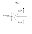
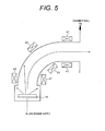
- the filtered AIP method is performed using an apparatus in which a part of an arc evaporation source 14 of the film formation apparatus 100, which is shown in Fig. 3 , is constituted as shown in Figs. 4 and 5 (hereinafter appropriately referred to as a filtered film formation apparatus).
- the filtered film formation apparatus has a duct comprising a magnetic induction mechanism composed of a plurality of electromagnetic coils 41, in front of the arc evaporation source 14.
- the duct comprising the magnetic induction mechanism, the metal particles which are liable to be discharged at a small angle to a surface of the target can be trapped with the duct.
- only ionized target atoms can be induced to the substrate 1a by a magnetic field.
- the shape of the duct may be linear (a linear type arc evaporation source) as shown in Fig. 4 , or may be curved at 90° (a 90° curved type evaporation source) as shown in Fig. 5 . Further, the shape thereof may be curved at an angle of more than 90°.
- test material Nos. 2, 4, 6, 8 to 10, 13 to 21, 23, 24 and 26 to 46 in which the effects of the invention have been confirmed
- Comparative Examples test material Nos. 1, 3, 5, 7, 11, 12, 22 and 25
- Hard films shown in Tables 1 to 3 were each formed on a substrate composed of die steel (JIS-SKD 11, HRC60), using the film formation apparatus shown in Fig. 3 ("conventional arc” in Tables), the film formation apparatus mounting the linear type arc evaporation source shown in Fig. 4 ("filtered 1" in Tables), the film formation apparatus mounting the 90° curved type arc evaporation source shown in Fig. 5 (“filtered 2" in Tables) or a holocathode type film formation apparatus (“HCD” in Tables).
- the substrate was first placed in the film formation apparatus, and the inside of the chamber was exhausted to 1 ⁇ 10 -3 Pa or less. Thereafter, the substrate was heated to 400°C, and then subjected to sputter cleaning using Ar ions. After nitrogen was introduced into the chamber to 4 Pa, arc discharge was performed at a current of 150 A to form the hard film on the substrate.
- some test materials were subjected to polishing with a polishing apparatus. Further, before the hard film formation, CrN film formation was performed for some test materials. After the film formation or after the polishing, the composition of the hard film, the number of metal particles, the maximum peak height (Rp) and the hardness (GPa) were measured, and a shearing test was performed.
- the composition of the hard film was measured with an EPMA (Electron Probe Micro Analyzer).
- 10 line segments having a length of 10 mm were arbitrarily selected on a surface of the hard film formed on a region of the curved surface of the test material (shearing die) and a region from the end part of the curved surface on the side facing to the surface of the sheet or plate material to 300 ⁇ m along the surface of the substrate. Then, a cross section of the hard film cut in a direction perpendicular to the curved surface from the line segment was observed using an optical microscope at a magnification of 400 times, and the number of metal particles having a diameter of 20 ⁇ m or more which were exposed on the cross section was counted. Then, an average value of the numbers of metal particles in the 10 line segments was calculated, and the average value was taken as the number of metal particles.
- the hardness (Vickers hardness) was measured using a Vickers indenter under conditions of a load of 25 gf and a retention time of 15 seconds.
- the maximum peak height (Rp) was measured using a stylus surface roughness meter, DEKTAK 6M, manufactured by Sloan, at a scanning distance of 1 mm.
- the shearing test of a high-tensile steel sheet having a tensile strength of 980 MPa, a thickness of 2 mm and a width of 100 mm was performed.
- a shearing test was constructed so that the steel sheet was sheared by the pair of test materials disposed in the upper side and lower side of the steel sheet, and the test was performed under conditions that the stroke number was 90 spm, and that the clearance between the test materials was 10% (0.2 mm) of the thickness of the steel sheet.
- the size of shear surfaces of the test materials was 150 mm (the length in a direction cutting the steel sheet) ⁇ 100 mm.
- test materials shown in Table 1 were polished to a maximum peak height (Rp) of 0.6 to 0.8 ⁇ m. Further, all test materials shown in Table 2 had a metal particle number of 2 or less. Furthermore, all test materials shown in Table 3 were polished to a maximum peak height (Rp) of 0.5 ⁇ m or less and had a metal particle number of 2 or less.
- the composition of the hard films met the composition specified in the invention, and both the thickness of the hard films and the number of metal particles were within the ranges specified in the invention. Accordingly, the life of the shearing dies was 35,000 or more, resulting in good evaluation.
- the composition of the hard films was not the composition specified in the invention, so that the life of the shearing dies was less than 35,000, resulting in poor evaluation.
- the thickness of the hard films exceeded the range specified in the invention, so that the life of the shearing dies was less than 35,000, resulting in poor evaluation.
Landscapes
- Engineering & Computer Science (AREA)
- Chemical & Material Sciences (AREA)
- Mechanical Engineering (AREA)
- Materials Engineering (AREA)
- Chemical Kinetics & Catalysis (AREA)
- Metallurgy (AREA)
- Organic Chemistry (AREA)
- Inorganic Chemistry (AREA)
- Physical Vapour Deposition (AREA)
- Cutting Tools, Boring Holders, And Turrets (AREA)
- Mounting, Exchange, And Manufacturing Of Dies (AREA)
Abstract
Description
- This application claims priority from Japanese Patent Application No.
2010-147187 filed on June 29, 2010 - The present invention relates to a shearing die for shearing a sheet or plate material, and a method for manufacturing the shearing die.
- With an increase in strength of metal materials such as high-tensile steel products, the shortened life of shearing dies used for shearing of sheet or plate materials composed of the metal materials have become a problem. Accordingly, in order to solve this problem, techniques of forming various hard films as described below on substrates of the dies have now been created.
- For example,
Patent Document 1 discloses a technique of forming a ceramic of any one of carbides, nitrides and carbonitrides of the group IV elements on a substrate surface of a shearing flat-blade knife. Further,Patent Document 2 discloses a technique of forming a ceramic of a titanium nitride as an inner layer, a titanium metal layer as an intermediate layer and a ceramic of a titanium nitride as an outer layer on a substrate surface of a shearing flat-blade knife. - Furthermore, Patent Document 3 discloses a method for manufacturing a die for punch press, in which after heat treatment, cutting, electric discharge working and the like are performed to a substrate of the die, a nitride layer is formed by ion nitriding on a cutting blade part of the die or a contact part of the die with a sheet or plate material, and thereafter ion plating is performed with titanium evaporating particles, thereby forming a film of a nitride, carbide or carbonitride of titanium on a surface part of the die.
- It has been conceivable herein that the main causes for damage of a shearing die are fatigue fracture of the die caused by repeated application of impact and wear of a cutting blade part of the die caused by friction with a sheared sheet or plate material. Accordingly, the damage of the shearing die can be decreased to some degree by applying the hard films having high hardness disclosed in
Patent Documents 1 to 3 to the shearing die. -
- Patent Document 1:
JP-A-8-325706 - Patent Document 2:
JP-A-8-325707 - Patent Document 3:
JP-A-2000-343151 - However, in the techniques disclosed in
Patent Documents 1 to 3, the carbides, nitrides or carbonitrides of the group IV elements are used as the hard films, so that the dies have a hardness of about 2,500 HV (Vickers Hardness), and this hardness is insufficient. Accordingly, the techniques disclosed inPatent Documents 1 to 3 still remain to have a problem in terms of longer life.
Further, in the technique disclosed in Patent Document 3, the hard thin film is formed after hardening treatment of the substrate by ion nitriding. However, since the substrate itself is cured, the whole die becomes rather brittle, thereby promoting early breakage of the die. - In addition, the shearing die usually has a right-angled or acute-angled shearing part, different from a plastic forming die such as a bending or drawing die, and a stress applied to the shearing die is also different from that applied to the plastic forming die. Accordingly, a surface treatment technique specific to the shearing die becomes necessary.
- The invention has been made in view of the above-mentioned problems, and an object thereof is to provide a shearing die having longer life and a method for manufacturing the same.
- The present invention provides the following shearing die and method for manufacturing the same.
- (1) A shearing die comprising a pair of substrates, which is used for shearing a sheet or plate material disposed therebetween by the pair of substrates,
wherein at least one of the substrates is composed of a steel, a cemented carbide or a ceramic, and said at least one of the substrates comprise a blade edge having a shape of a curved surface for shearing the sheet or plate material and a surface continuing from the curved surface and facing to a surface of the sheet or plate material,
a hard film formed by an arc ion plating method is provided at least on a region of the curved surface and a region from the end part of the curved surface on the side facing to the surface of the sheet or plate material to 300 µm along the surface of the substrate, of the surface of said at least one of the substrates, and
the hard film comprises Al and one or more of Ti and Cr, and has a thickness of 1 µm or more and 5 µm or less, and the number of a metal particle having a diameter of 20 µm or more, which is present on a line segment having a length of 10 mm on a surface of the hard film formed on the region of the curved surface and the region from the end part of the curved surface on the side facing to the surface of the sheet or plate material to 300 µm along the surface of the substrate, is 2 or less. - As describe above, in the shearing die according to the invention, the hard film is formed at least on the region of the curved surface and the region from the end part of the curved surface on the side facing to the surface of the sheet or plate material to 300 µm along the surface of the substrate, whereby a region to which a high stress is applied, of the surface which comes into contact with the sheet or plate material at the time of shearing the sheet or plate material, can be properly protected.
- Further, the hard film of the shearing die according to the invention comprises Al and one or more of Ti and Cr, so that the shearing die can be protected by the hard film having excellent wear resistance and durability. Further, the hard film of the shearing die according to the invention has a thickness of 1 µm or more and 5 µm or less, so that separation or breakage of the film can be avoided from occurring in an interface between the substrate and the hard film or in the inside of the hard film.
- Furthermore, in the hard film of the shearing die according to the invention, the number of metal particles contained in the hard film formed on the region of the curved surface and the region from the end part of the curved surface on the side facing to the surface of the sheet or plate material to 300 µm along the surface of the substrate is limited to the specific number, thereby being able to inhibit damage of the hard film at the time of shearing the sheet or plate material.
-
- (2) The shearing die according to (1), wherein a maximum peak height (Rp) of the surface of the hard film as a parameter of the surface roughness is 1.0 µm or less.
-
- (3) The shearing die according to (1) or (2), wherein the hard film is composed of (TiaCrbAlcSid)(C1-xNx), satisfying:
- 0≤a≤0.3;
- 0.1≤b≤0.5;
- 0.3≤c≤0.7;
- 0≤d≤0.2;
- a+b+c+d=1; and
- 0.7≤x≤1,
- As described above, the hard film of the shearing die according to the invention has the above-mentioned composition, thereby being able to improve wear resistance and durability.
-
- (4) The shearing die according to any one of (1) to (3), wherein a CrN film having a thickness of 1 µm or more and 5 µm or less is further provided between the hard film and the substrate.
As described above, the shearing die according to the invention comprises the CrN film, thereby being able to improve adhesiveness between the substrate and the hard film. -
- (5) A method for manufacturing a shearing die which comprises a pair of substrates and is used for shearing a sheet or plate material disposed therebetween by the pair of substrates,
wherein at least one of the substrates is composed of a steel, a cemented carbide or a ceramic, and said at least one of the substrates comprise a blade edge having a shape of a curved surface for shearing the sheet or plate material and a surface continuing from the curved surface and facing to a surface of the sheet or plate material, and
the method comprises forming a hard film comprising Al and one or more of Ti and Cr at least on a region of the curved surface and a region from the end part of the curved surface on the side facing to the surface of the sheet or plate material to 300 µm along the surface of the substrate, of the surface of said at least one of the substrates, by a filtered arc ion plating method. - As described above, the method for manufacturing a shearing die according to the invention comprises forming the hard film by the filtered arc ion plating method, thereby being able to form the hard film having a small number of metal particles on the surface of the substrate.
- According to the shearing die according to the invention, a hard film having excellent wear resistance and durability is formed on specific regions of a surface of a substrate, thereby being able to achieve longer life of the shearing die. Further, according to the method for manufacturing a shearing die according to the invention, the shearing die having longer life can be manufactured.
-
-
Fig. 1 is a cross-sectional view showing a shearing die according to the invention and a sheet or plate material in a course of shearing the sheet or plate material by the shearing die. -
Fig. 2 is an enlarged cross-sectional view showing a shearing die according to the invention and a sheet or plate material in a course of shearing the sheet or plate material by the shearing die. -
Fig. 3 is a schematic view showing an arc ion plating apparatus used in a manufacturing method of a shearing die according to the invention. -
Fig. 4 is a schematic view showing a linear type arc evaporation source of a filtered arc ion plating apparatus used in a method for manufacturing a shearing die according to the invention. -
Fig. 5 is a schematic view showing a 90° curved type arc evaporation source of a filtered arc ion plating apparatus used in a method for manufacturing a shearing die according to the invention. -
- 1: Shearing Die
- 1a: Substrate
- 1b: Hard film
- 2: Sheet or plate material
- 11: Exhaust port
- 12: Gas supply port
- 13: Chamber
- 13a: Chamber wall
- 14: Arc evaporation source
- 15: Arc power supply
- 16: Substrate stage
- 17: Supporting table
- 18: Bias power supply
- 19: Heater
- 20: Filament
- 21: Filament discharge power supply
- 22: Filament heating power supply
- 41: Electromagnetic coil
- 100: Film formation apparatus
- Embodiments for carrying out the shearing die according to the invention and the manufacturing method thereof will be described in detail below with appropriate reference to the drawings.
- The shearing die 1 according to the invention is a die attached to a shearing machine (mechanical type, hydraulic type or the like) and for separating a material showing a sheet or plate shape (a sheet or plate material) by stress (shearing stress). Then, the shearing die 1 according to the invention comprises
substrates hard films substrates Figs. 1 and2 .
Incidentally, in order to protect both thesubstrates hard film 1b is formed on both thesubstrates - In this embodiment, an example of applying the invention to the shearing die 1 showing a shape in which a face facing to a sheet or
plate material 2 approximately linearly extends in a direction perpendicular to paper ofFigs. 1 and2 (so-called linear blade) is described below. However, the shape of the shearing die 1 is not limited to the above-mentioned shape. The invention can also be applied, for example, to the shearing die 1 showing a shape in which the face facing to the sheet orplate material 2 extends in an arc in a direction perpendicular to paper ofFigs. 1 and2 (so-called rotary blade), as long as it is a die which shears the sheet or plate material by shearing stress. - The
substrate 1a of the shearing die 1 will be described below. - The
substrate 1a of the shearing die 1 is composed of a steel, a cemented carbide or a ceramic. The steel as used herein is an alloy comprising Fe as a main component. Here, an alloy comprising Fe as a main component generally means that an alloy comprises Fe in an amount of more than 50% by mass. Further, the cemented carbide is an alloy produced by sintering hard metal carbide. The specific example of the hard metal carbide constituting the cemented carbide includes WC (tungsten carbide). In addition, WC in which a slight amount of TiC (titanium carbide) or TaC (tantalum carbide) is contained is also exemplified as the hard metal carbide. - The
substrate 1a of the shearing die 1 comprises a blade edge having a shape of a curved surface for shearing the sheet orplate material 2 and a surface continuing from the curved surface and facing to a surface of the sheet orplate material 2. The blade edge means an edge part of thesubstrate 1a which shears the sheet orplate material 2. Then, in order to decrease damage of the sheet orplate material 2 at the time of shearing, the blade edge shows a shape of the curved surface in cross section (seeFig. 2 ).
Incidentally, of a pair ofsubstrates - The overall shape of the
substrate 1a of the shearing die 1 is not particularly limited, as long as it is possible to shear the sheet or plate material by shearing stress, as described above. For example, it is an approximate rectangular parallelepiped shape, an approximate disc shape or the like. Further, the pair ofsubstrates - Furthermore, the blade edge (edge for shearing the sheet or plate material 2) of the
substrate 1a of the shearing die 1 is not limited to one showing a right angle as shown inFigs. 1 and2 , and may be one showing an acute angle (less than 90°). Here, in the case where thesubstrate 1a comprises a blade edge having a shape of a curved surface, the blade edge showing a right angle means that an angle formed at the blade edge by extending two surfaces, each of which continues from the curved surface, shows a right angle. - The
hard film 1b of the shearing die 1 will be described below. - The
hard film 1b of the shearing die 1 is formed at least on a region of the curved surface and a region from the end part of the curved surface on the side facing to the surface of the sheet orplate material 2 to 300 µm along the surface of thesubstrate 1a (the above-mentioned two regions may be hereinafter referred to as a protection region hereinafter), of the surface of thesubstrate 1a. - The reason for this is that when the sheet or
plate material 2 is sheared by using the shearing die 1 as shown inFig. 2 , a high stress is particularly applied to the protection region, of a region where the shearing die 1 and the sheet orplate material 2 come into contact with each other.
Here, a region in which thehard film 1b is formed has only to include at least the protection region. Thus, for example, thehard film 1b may be provided on thewhole substrate 1a of the shearing die 1. - Incidentally,
Fig. 2 shows stress distribution at the edge (edge for shearing the sheet or plate material 2) of thesubstrate 1a of the shearing die 1, and the range to which a high stress is applied is the region of the curved surface and the narrow range from an end part of the curved surface (within 300 µm from the end part of the curved surface along the surface of the substrate). Accordingly, for the shearing die 1 in which the edge of thesubstrate 1 a has an angle of 90° or less, improvements in wear resistance and durability can be secured by forming thehard film 1b at least on the protection region. Here, in the case where thesubstrate 1a comprises a blade edge having a shape of a curved surface, the angle of the edge of thesubstrate 1a means that an angle formed at the edge of thesubstrate 1a by extending two surfaces, each of which continues from the curved surface, shows a right angle. - The
hard film 1b comprises Al and one or more of Ti and Cr. The reason for such a requirement is that Al is an essential element for improving wear resistance of thehard film 1b, and that Ti and Cr are elements for improving wear resistance and durability of thehard film 1b.
Specifically, thehard film 1b is a film of (Ti, Al)(CN), (Cr, Al)(CN) or (Ti, Cr, Al)(CN), or a film thereof in which Si is allowed to be contained. Of these, preferred one is a film in which both of Ti and Cr are contained. - Further, the
hard film 1b is preferably composed of (TiaCrbAlcSid)(C1-xNx), satisfying 0≤a≤0.3, 0.1 ≤b≤0.5, 0.3≤c≤0.7, 0≤d≤0.2, a+b+c+d=1 and 0.7≤x≤1 (wherein a indicates an atom ratio of Ti, b indicates an atom ratio of Cr, c indicates an atom ratio of Al, d indicates an atom ratio of Si, and x indicates an atom ratio of N). Thehard film 1b having the above-mentioned composition can further improve wear resistance and durability thereof.
The reason for restricting the above-mentioned composition will be described in detail below. - Al and Cr improve wear resistance of the
hard film 1b by forming an (Al, Cr)(CN) film, so that the atom ratio c of Al in the above-mentioned composition formula is preferably 0.3≤c≤0.7, and the atom ratio b of Cr is preferably 0.1≤b≤0.5. More preferably, the atom ratio c of Al is 0.4≤c≤0.6, and the atom ratio b of Cr is 0.15≤b≤0.3. - Ti is an element for increasing the hardness of the
hard film 1b to improve wear resistance. However, the excessive content thereof may make thehard film 1b brittle. Accordingly, the atom ratio a of Ti in the above-mentioned composition formula is preferably 0≤a≤0.3. - Si is an element for refining crystals in the
hard film 1b, thereby improving hardness and resistance to high contact pressure. However, the excessive content thereof may make thehard film 1b amorphous. Accordingly, the atom ratio d of Si in the above-mentioned composition formula is preferably 0≤d≤0.2. More preferably, the atom ratio d of Si is 0≤d≤0.15.
Incidentally, taking it into consideration that thehard film 1b is made amorphous by an increase in the Si content, it is further preferred that for the atom ratio c of Al and the atom ratio d of Si in the above-mentioned composition formula, (c+d) is 0.6 or less. - C is an element for increasing the hardness of the
hard film 1b to improve wear resistance. However, the excessive content thereof may cause the hardness of thehard film 1b to decrease. Accordingly, the atom ratio (1-x) of C in the above-mentioned composition formula is preferably less than 0.3, namely 0.7≤x≤1. - When the
hard film 1b is formed on the surface of thesubstrate 1a by an arc ion plating method (or a filtered arc ion plating method), a residual compression stress is generated in thehard film 1b. In particular, when thehard film 1b is formed thickly on the curved surface provided at the edge for shearing the sheet orplate material 2, of the surface of thesubstrate 1a, separation or a fracture phenomenon occurs in an interface (an interface between thesubstrate 1a and thehard film 1b) or in the inside of thehard film 1b.
Accordingly, the thickness of thehard film 1b is required to be 1 µm or more and 5 µm or less. More preferably, it is 1 µm or more and 3 µm or less.
Incidentally, the thickness of thehard film 1b can be controlled by the film formation method described later. - A metal particles having a diameter of 20 µm or more, which is present in the
hard film 1b, causes damage of thehard film 1b. Further, it is necessary to inhibit the presence of the metal particle in thehard film 1b formed on the region of the curved surface to which the highest stress is applied at the time of shearing the sheet orplate material 2 by the shearing die 1 and the region from the end part of the curved surface on the side facing to the surface of the sheet orplate material 2 to 300 µm along the surface of the substrate. - Accordingly, the damage of the
hard film 1b at the time of shearing the sheet orplate material 2 can be inhibited by restricting the number of metal particle having a diameter of 20 µm or more, which is present on a line segment having a length of 10 mm on a surface of the hard film formed on the region of the curved surface and the region from the end part of the curved surface on the side facing to the surface of the sheet or plate material to 300 µm along the surface of the substrate, to 2 or less. More preferably, the number of metal particle is 0. Then, the number of metal particle having a diameter of 20 µm or more can be controlled by the film formation method described later.
Incidentally, the metal particle is an aggregate of metals such as Ti, Cr and Al which are present in thehard film 1b. - Here, the metal particle which is present on a line segment having a length of 10 mm means a metal particle completely cut with the line segment.
Further, the diameter is a diameter of a cross section of the metal particle at the time when the metal particle is viewed from a direction perpendicular to the surface of thehard film 1b. When the shape of the cross section is not circular, the longest length (span) between both ends is taken as the diameter.
Incidentally, it is preferred that the line segment is set in the approximately same direction as a direction in which the blade edge (edge) extends (a ridge line direction), on the surface of thehard film 1b formed on the region of the curved surface and the region from the end part of the curved surface on the side facing to the surface of the sheet or plate material to 300 µm along the surface of the substrate. - In the shearing die 1, the contact region with the sheet or
plate material 2 is concentrated in a narrow region in a vicinity of the edge (blade edge), different from a plastic forming die (such as a bending or drawing die) in which the contact region with the sheet orplate material 2 is large. Accordingly, a stress applied to that region is very large. Then, the stress acts in a direction approximately perpendicular to a surface of the die. Accordingly, when the surface of thehard film 1b has an unevenness, the stress is concentrated on convex portions, thereby easily causing damage of the film.
Accordingly, the maximum peak height (Rp) of thehard film 1b is preferably 1 µm or less. More preferably, it is 0.5 µm or less. The maximum peak height (Rp) is further more preferably 0 µm since thehard film 1b having the flatter surface is preferred. However, from the stand point of the easiness of production, thehard film 1b having the maximum peak height (Rp) of 0.05 µm or more can be preferably used. The maximum peak height (Rp) is defined in JIS B 0601 (2001). - The maximum peak height is a maximum value of peak heights of a profile curve in a reference length. The maximum peak height (Rp) is measured in any three places with a stylus surface roughness meter, Dektak 6M, manufactured by Sloan (at a scanning length of 1 mm, a scanning rate of 1 mm/15 sec and a load of 20 mgf), and the average value thereof is calculated.
It is more preferred that the measurement is performed to thehard film 1 b formed on the region of the curved surface for shearing the sheet orplate material 2 and the region from the end part of the curved surface on the side facing to the surface of the sheet orplate material 2 to 300 µm along the surface of the substrate, of the surface of thehard film 1b. - The
hard film 1b comprises Al in order to increase the hardness, so that residual stress is also increased. As a result, there is a tendency that adhesiveness of thesubstrate 1a to thehard film 1b is decreased. It is therefore preferred to form an intermediate layer (not shown in Figure) composed of CrN between thesubstrate 1a and thehard film 1b, in order to improve adhesiveness of thesubstrate 1a to thehard film 1b. Further, when the thickness of the CrN film is less than 1 µm, effects of improving the adhesiveness and decreasing the residual stress may be small. On the other hand, when it exceeds 5 µm, these effects may be saturated. Accordingly, the thickness of the CrN film is preferably from 1 to 5 µm. - Incidentally, the CrN film comprises Cr and N as main components (for example, the total atomic percent of Cr and N is 80 at% or more, and more preferably 90 at% or more). As the content ratio of Cr and N, it is represented as Cr1-xNx wherein x is 0.3 to 0.55.
- The manufacturing method of the shearing die 1 will be described below.
- The shearing die 1 is manufactured by forming the
hard film 1b at least on the protection region of thesubstrate 1a, of the surface of thesubstrate 1a, by the arc ion plating method (hereinafter appropriately referred to as the AIP method). The AIP method as used herein is a film formation method of coating the surface of the substrate with an ion evaporation material by utilizing arc discharge.
Thehard film 1b can be properly formed on the surface of thesubstrate 1a by using the AIP method. Further, it is preferred that after the formation of thehard film 1b by the AIP method, the surface of thehard film 1b is smoothened by polishing to a maximum peak height (Rp) of 1.0 µm or less. - Furthermore, among the AIP methods, it is preferred to apply the filtered arc ion plating method (hereinafter appropriately referred to as the filtered AIP method). The filtered AIP method as used herein is a kind of the AIP method and a film formation method of coating the surface of the
substrate 1a with an ion evaporation material while preventing metal particles (molten particles of a target) from adhering to thesubstrate 1a.
The use of the filtered AIP method allows to form thehard film 1b containing a markedly small amount of metal particles compared to the conventional AIP method, so that thehard film 1b having a low maximum peak height (Rp) can be obtained without performing the polishing after the film formation (or by the minimal polishing). The Rp of thehard film 1b after the film formation by the filtered AIP method is 2 µm or less, and is reduced to 0.1 µm or less by polishing thehard film 1b after the film formation. - For the shearing die 1 to which a high stress is applied, it is particularly effective to use the filtered AIP method.
The reason for this is as follows. When thehard film 1b comprising Al, Ti, Cr and the like is intended to be formed using the conventional AIP method, the metal particles (molten particles of the target) are scattered at the same time as the target is evaporated by arc discharge, because elements having different melting points are contained in the target, and the metal particles come to be mixed in thehard film 1b. As a result, unevenness is liable to be formed on the surface of thehard film 1b. Accordingly, when the film formation is performed using the conventional AIP method, it is preferred to smoothen the surface by polishing. However, in the case of the shearing die 1 having the acute-angled edge, polishing is extremely difficult in some cases. Accordingly, the filtered AIP method requiring no polishing (or minimum polishing) after the film formation is effective for the shearing die 1 to which a high stress is applied. - Incidentally, in the case of forming the CrN film, the CrN film is first formed on the surface of the
substrate 1a by the AIP method or the filtered AIP method, and thereafter, thehard film 1b is formed thereon by the same method. - The arc ion plating method and the filtered arc ion plating method will be described in detail below with reference to
Figs. 3 ,4 and5 . - The arc ion plating method is performed using a
film formation apparatus 100 shown inFig. 3 . - As shown in
Fig. 3 , thefilm formation apparatus 100 comprises achamber 13 having anexhaust port 11 for vacuum exhaust and agas supply port 12 for supplying N2 gas, Ar gas, CH4 gas or the like, arc power supplies 15 connecting toarc evaporation sources 14, supporting tables 17 provided on asubstrate stage 16, for supporting bodies to be treated (not shown in Figure) which are bodied to be film-formed, and abias power supply 18 for applying negative bias voltage to the bodies to be treated through the supporting tables 17 between the supporting tables 17 and thechamber 13. In addition, thefilm formation apparatus 100 comprisesheaters 19, afilament 20, a filamentdischarge power supply 21 and a filamentheating power supply 22. - First, targets are each attached to the
arc evaporation sources 14 of thefilm formation apparatus 100, andsubstrates 1a are each attached as the bodies to be treated (not shown in Figure) onto the supporting tables 17 on therotating substrate stage 16. The inside of thechamber 13 is evacuated (exhausted to 1×10⁻³ Pa or less) to a vacuum state. Then, the bodies to be treated are heated to a temperature of about 400°C with theheaters 19 in thechamber 13. Thereafter, an arc current of 150 A is supplied from thearc evaporation sources 14 to the targets having a diameter of 100 mm in a N2 atmosphere, an Ar atmosphere, a CH4 atmosphere or a mixed gas atmosphere thereof, having a total pressure of 4 Pa, thereby forminghard films 1b on thesubstrates 1a. - The filtered AIP method is performed using an apparatus in which a part of an
arc evaporation source 14 of thefilm formation apparatus 100, which is shown inFig. 3 , is constituted as shown inFigs. 4 and5 (hereinafter appropriately referred to as a filtered film formation apparatus). - The filtered film formation apparatus has a duct comprising a magnetic induction mechanism composed of a plurality of
electromagnetic coils 41, in front of thearc evaporation source 14. By having the duct comprising the magnetic induction mechanism, the metal particles which are liable to be discharged at a small angle to a surface of the target can be trapped with the duct. As a result, only ionized target atoms can be induced to thesubstrate 1a by a magnetic field.
In thearc evaporation source 14, the shape of the duct may be linear (a linear type arc evaporation source) as shown inFig. 4 , or may be curved at 90° (a 90° curved type evaporation source) as shown inFig. 5 . Further, the shape thereof may be curved at an angle of more than 90°. - While embodiments of the invention have been described above, the invention is not limited to the above-mentioned embodiments, and variations may be appropriately made without departing from the gist of the invention described in the claims.
- The shearing die and the manufacturing method thereof according to the invention will be specifically described below, by contrasting Examples (test material Nos. 2, 4, 6, 8 to 10, 13 to 21, 23, 24 and 26 to 46), in which the effects of the invention have been confirmed, to Comparative Examples (test material Nos. 1, 3, 5, 7, 11, 12, 22 and 25), in which the requirements of the invention are not satisfied.
- Hard films shown in Tables 1 to 3 were each formed on a substrate composed of die steel (JIS-
SKD 11, HRC60), using the film formation apparatus shown inFig. 3 ("conventional arc" in Tables), the film formation apparatus mounting the linear type arc evaporation source shown inFig. 4 ("filtered 1" in Tables), the film formation apparatus mounting the 90° curved type arc evaporation source shown inFig. 5 ("filtered 2" in Tables) or a holocathode type film formation apparatus ("HCD" in Tables). - As a film formation method, the substrate was first placed in the film formation apparatus, and the inside of the chamber was exhausted to 1×10⁻³ Pa or less. Thereafter, the substrate was heated to 400°C, and then subjected to sputter cleaning using Ar ions. After nitrogen was introduced into the chamber to 4 Pa, arc discharge was performed at a current of 150 A to form the hard film on the substrate. Incidentally, after the hard film formation, some test materials were subjected to polishing with a polishing apparatus. Further, before the hard film formation, CrN film formation was performed for some test materials.
After the film formation or after the polishing, the composition of the hard film, the number of metal particles, the maximum peak height (Rp) and the hardness (GPa) were measured, and a shearing test was performed. - The composition of the hard film was measured with an EPMA (Electron Probe Micro Analyzer).
- For the number of metal particles, 10 line segments having a length of 10 mm were arbitrarily selected on a surface of the hard film formed on a region of the curved surface of the test material (shearing die) and a region from the end part of the curved surface on the side facing to the surface of the sheet or plate material to 300 µm along the surface of the substrate. Then, a cross section of the hard film cut in a direction perpendicular to the curved surface from the line segment was observed using an optical microscope at a magnification of 400 times, and the number of metal particles having a diameter of 20 µm or more which were exposed on the cross section was counted. Then, an average value of the numbers of metal particles in the 10 line segments was calculated, and the average value was taken as the number of metal particles.
- The hardness (Vickers hardness) was measured using a Vickers indenter under conditions of a load of 25 gf and a retention time of 15 seconds.
The maximum peak height (Rp) was measured using a stylus surface roughness meter, DEKTAK 6M, manufactured by Sloan, at a scanning distance of 1 mm. - Using the test material (linear blade) prepared by the above-mentioned method, the shearing test of a high-tensile steel sheet having a tensile strength of 980 MPa, a thickness of 2 mm and a width of 100 mm was performed. A shearing test was constructed so that the steel sheet was sheared by the pair of test materials disposed in the upper side and lower side of the steel sheet, and the test was performed under conditions that the stroke number was 90 spm, and that the clearance between the test materials was 10% (0.2 mm) of the thickness of the steel sheet.
Incidentally, the size of shear surfaces of the test materials was 150 mm (the length in a direction cutting the steel sheet) × 100 mm. - As the evaluation method, damage of the shear surfaces (the whole area of a part which came into contact with the steel sheet) was observed at given time intervals, and the time when the damage of 200 µm or more occurred in that part was judged as the life of the test materials.
The case where the tool life (the stroke number until the occurrence of the damage) was 35,000 or more was evaluated as good, and the case where the tool life was less than 35,000 was evaluated as poor. - Incidentally, all test materials shown in Table 1 were polished to a maximum peak height (Rp) of 0.6 to 0.8 µm. Further, all test materials shown in Table 2 had a metal particle number of 2 or less. Furthermore, all test materials shown in Table 3 were polished to a maximum peak height (Rp) of 0.5 µm or less and had a metal particle number of 2 or less.
-
Table 1 Test Material No. Deposition System Hard Film CrN Film Hardness (GPa) Polishing Number of Metal Particles Tool Life (Stroke Number) Composition Thickness (µm) Formed or Not formed Thickness (µm) 1 Conventional arc (Ti0.5Al0.5)N 3 Not formed - 2,800 Polished 5 5,000 Comparative Example 2 Filtered 1 (Ti0.5Al0.5)N 3 Not formed - 3,000 Polished 1 120,000 Example 3 Conventional arc (Cr0.5Al0.5)N 3 Not formed - 2,800 Polished 4 8,000 Comparative Example 4 Filtered 1 (Cr0.5Al0.5)N 3 Not formed - 3,100 Polished 2 65,000 Example 5 Conventional arc (Ti0.2Cr0.2Al0.6)N 3 Formed 2 3,300 Polished 4 9,000 Comparative Example 6 Filtered 1 (Ti0.2Cr0.2Al0.6)N 3 Formed 2 3,500 Polished 0 220,000 Example 7 Conventional arc (Ti0.2Cr0.2Al0.55Si0.05)N 3 Formed 2 3,400 Polished 5 12,000 Comparative Example 8 Filtered 1 (Ti0.2Cr0.2A10.55Si0.05)N 3 Formed 2 3,600 Polished 0 250,000 Example 9 Filtered 1 (Ti0.2Cr0.2Al0.55 Si0.05)N 3 Formed 2 3,600 Polished 1 180,000 Example 10 Filtered 2 (Ti0.2Cr0.2Al0.55Si0.05)N 3 Formed 2 3,600 Polished 0 210,000 Example -
Table 2 Test Material No. Deposition System Hard Film CrN Film Hardness (GPa) Polishing Rp (µm) Tool Life (Stroke Number) Composition Thickness (µm) Formed or Not formed Thickness (µm) 11 HCD TiN 3 Not formed - 2,200 Not polished 0.5 3,000 Comparative Example 12 Filtered 1 CrN 3 Not formed - 1,500 Polished 0.6 30,000 Comparative Example 13 Filtered 1 (Ti0.5Al0.5)N 3 Not formed - 2,800 Not polished 1.2 50,000 Example 14 Filtered 1 (Ti0.5Al0.5)N 3 Not formed - 2,800 Polished 0.6 75,000 Example 15 Filtered 1 (Cr0.5Al0.5)N 3 Not formed - 2,800 Not polished 2.2 50,000 Example 16 Filtered 1 (Cr0.5Al0.5)N 3 Not Formed - 2,800 Polished 0.7 70,000 Example 17 Filtered 1 (Ti0.2Cr0.2Al0.6)N 3 Not formed - 3,300 Not polished 2.3 60,000 Example 18 Filtered 1 (Ti0.2Cr0.2Al0.6)N 3 Not formed - 3,300 Polished 1.5 80,000 Example 19 Filtered 1 (Ti0.2Cr0.2Al0.6)N 3 Not formed - 3,300 Polished 0.8 110,000 Example 20 Filtered 1 (Ti0.2Cr0.2Al0.6)N 3 Not formed - 3,300 Polished 0.65 130,000 Example 21 Filtered 1 (Ti0.2Cr0.2Al0.6)N 3 Not formed - 3,300 Polished 0.3 200,000 Example 22 Filtered 1 (Ti0.2Cr0.2Al0.6)N 0.5 Not formed - 3,300 Polished 0.25 13,000 Comparative Example 23 Filtered 1 (Ti0.2Cr0.2Al0.6)N 1.5 Not formed - 3,300 Polished 0.25 20,000 Example 24 Filtered 1 (Ti0.2Cr0.2Al0.6)N 4 Not Formed - 3,300 Polished 0.4 210,000 Example 25 Filtered 1 (Ti0.2Cr0.2Al0.6)N 7 Not formed - 3,300 Polished 0.55 32,000 Comparative Example 26 Filtered 1 (Ti0.2Cr0.2Al0.6)C0.2N0.8 4 Not formed - 3,300 Polished 0.55 150,000 Example -
Table 3 Test Material No. Deposition System Hard Film CrN Film Hardness (GPa) Tool Life (Stroke Number) Composition Thickness (µm) Formed or Not formed Thickness (µm) 27 Filtered 1 (Ti0.2Cr0.2Al0.6)N 3 Not formed - 3,300 120,000 Example 28 Filtered 1 (Ti0.2Cr0.2Al0.6)N 3 Formed 2 3,300 180,000 Example 29 Filtered 1 (Ti0.2Cr0.2Al0.6)N 3 Formed 0.5 3,300 120,000 Example 30 Filtered 1 (Ti0.2Cr0.2Al0.6)N 3 Formed 4 3,300 180,000 Example 31 Filtered 1 (Ti0.2Cr0.2Al0.6)N 3 Formed 7 3,300 110,000 Example 32 Filtered 1 (Ti0.35Cr0.35Al0.3)N 3 Formed 2 2,500 60,000 Example 33 Filtered 1 (Ti0.25Cr0.25Al0.5)N 3 Formed 2 3,200 80,000 Example 34 Filtered 1 (Ti0.2Cr0.2Al0.6)N 3 Formed 2 3,300 120,000 Example 35 Filtered 1 (Ti0.1Cr0.1Al0.8)N 3 Formed 2 2,400 60,000 Example 36 Filtered 1 (Ti0.4Cr0.1A10.5)N 3 Formed 2 2,700 50,000 Example 37 Filtered 1 (Ti0.3Cr0.2Al0.5)N 3 Formed 2 3,000 90,000 Example 38 Filtered 1 (Ti0.1Cr0.5Al0.4)N 3 Formed 2 3,200 80,000 Example 39 Filtered 1 (Ti0.1Cr0.6Al0.3)N 3 Formed 2 2,600 55,000 Example 40 Filtered 1 (Ti0.2Cr0.2Al0.58Si0.02)N 3 Formed 2 3,300 220,000 Example 41 Filtered 1 (Ti0.2Cr0.2A10.55Si0.05)N 3 Formed 2 3,400 250,000 Example 42 Filtered 1 (Ti0.2Cr0.2Al0.5Si0.1)N 3 Formed 2 3,400 200,000 Example 43 Filtered 1 (Ti0.2Cr0.2Al0.4Si0.2)N 3 Formed 2 3,100 160,000 Example 44 Filtered 1 (Ti0.2Cr0.2Al0.3Si0.3)N 3 Formed 2 2,500 55,000 Example 45 Filtered 1 (Cr0.4Al0.55Si0.05)N 3 Formed 2 3,400 130,000 Example 46 Filtered 1 (Cr0.4Al0.6)N 3 Formed 2 3,300 70,000 Example - As shown in Table 1, in Test Material Nos. 2, 4, 6 and 8 to 10, the composition of the hard films met the composition specified in the invention, and both the thickness of the hard films and the number of metal particles were within the ranges specified in the invention. Accordingly, the life (stroke number) of the shearing dies was 35,000 or more, resulting in good evaluation.
On the other hand, in Test Material Nos. 1, 3, 5 and 7, the number of metal particles exceeded the range specified in the invention, so that the life of the shearing dies was less than 35,000, resulting in poor evaluation. - As shown in Table 2, in Test Material Nos. 13 to 21, 23, 24 and 26, the composition of the hard films met the composition specified in the invention, and both the thickness of the hard films and the number of metal particles were within the ranges specified in the invention. Accordingly, the life of the shearing dies was 35,000 or more, resulting in good evaluation.
On the other hand, in Test Material Nos. 11 and 12, the composition of the hard films was not the composition specified in the invention, so that the life of the shearing dies was less than 35,000, resulting in poor evaluation.
Further, in Test Material Nos. 22 and 25, the thickness of the hard films exceeded the range specified in the invention, so that the life of the shearing dies was less than 35,000, resulting in poor evaluation. - As shown in Table 3, in Test Material Nos. 27 to 46, the composition of the hard films met the composition specified in the invention, and both the thickness of the hard films and the number of metal particles were within the ranges specified in the invention. Accordingly, the life of the shearing dies was 35,000 or more, resulting in good evaluation.
- From the above results, it has been found that the life of shearing dies can be prolonged according to the shearing die and the method for manufacturing the shearing die according to the invention.
Claims (9)
- A shearing die comprising a pair of substrates, which is used for shearing a sheet or plate material disposed therebetween by the pair of substrates,
wherein at lease one of the substrates is composed of a steel, a cemented carbide or a ceramic, and said at least one of the substrates comprises a blade edge having a shape of a curved surface for shearing the sheet or plate material and a surface continuing from the curved surface and facing to a surface of the sheet or plate material,
a hard film formed by an arc ion plating method is provided at least on a region of the curved surface and a region from the end part of the curved surface on the side facing to the surface of the sheet or plate material to 300 µm along the surface of the substrate, of the surface of said at least one of the substrates, and
the hard film comprises Al and one or more of Ti and Cr, and has a thickness of 1 µm or more and 5 µm or less, and the number of a metal particle having a diameter of 20 µm or more, which is present on a line segment having a length of 10 mm on a surface of the hard film formed on the region of the curved surface and the region from the end part of the curved surface on the side facing to the surface of the sheet or plate material to 300 µm along the surface of the substrate, is 2 or less. - The shearing die according to claim 1, wherein a maximum peak height (Rp) of the surface of the hard film as a parameter of the surface roughness is 1.0 µm or less.
- The shearing die according to claim 1 or 2, wherein the hard film is composed of (TiaCrbAlcSid)(C1-xNx), satisfying:0≤a≤0.3;0.1≤b≤0.5;0.3≤c≤0.7;0≤d≤0.2;a+b+c+d=1; and0.7≤x≤1,wherein a indicates an atom ratio of Ti, b indicates an atom ratio of Cr, c indicates an atom ratio of Al, d indicates an atom ratio of Si, and x indicates an atom ratio ofN.
- The shearing die according to claim 1 or 2, wherein the hard film is composed of (TiaCrbAlcSid)(C1-xNx), satisfying:0≤a≤0.3;0.1 ≤b≤0.5;0.3≤c≤0.7;0≤d≤0.2;a+b+c+d=1; and0.7≤x≤1,wherein a indicates an atom ratio of Ti, b indicates an atom ratio of Cr, c indicates an atom ratio of Al, d indicates an atom ratio of Si, and x indicates an atom ratio of N.
- The shearing die according to claim 1, wherein a CrN film having a thickness of 1 µm or more and 5 µm or less is further provided between the hard film and the substrate.
- The shearing die according to claim 2, wherein a CrN film having a thickness of 1 µm or more and 5 µm or less is further provided between the hard film and the substrate.
- The shearing die according to claim 3, wherein a CrN film having a thickness of 1 µm or more and 5 µm or less is further provided between the hard film and the substrate.
- The shearing die according to claim 4, wherein a CrN film having a thickness of 1 µm or more and 5 µm or less is further provided between the hard film and the substrate.
- A method for manufacturing a shearing die which comprises a pair of substrates and is used for shearing a sheet or plate material disposed therebetween by the pair of substrates,
wherein at least one of the substrates is composed of a steel, a cemented carbide or a ceramic, and said at least one of the substrates comprise a blade edge having a shape of a curved surface for shearing the sheet or plate material and a surface continuing from the curved surface and facing to a surface of the sheet or plate material, and
the method comprises forming a hard film comprising Al and one or more of Ti and Cr at least on a region of the curved surface and a region from the end part of the curved surface on the side facing to the surface of the sheet or plate material to 300 µm along the surface of the substrate, of the surface of said at least one of the substrates, by a filtered arc ion plating method.
Applications Claiming Priority (1)
| Application Number | Priority Date | Filing Date | Title |
|---|---|---|---|
| JP2010147187A JP2012011393A (en) | 2010-06-29 | 2010-06-29 | Shearing die and method for manufacturing the same |
Publications (2)
| Publication Number | Publication Date |
|---|---|
| EP2402476A1 true EP2402476A1 (en) | 2012-01-04 |
| EP2402476B1 EP2402476B1 (en) | 2013-05-29 |
Family
ID=44645355
Family Applications (1)
| Application Number | Title | Priority Date | Filing Date |
|---|---|---|---|
| EP20110005313 Not-in-force EP2402476B1 (en) | 2010-06-29 | 2011-06-29 | Shearing die and method for manufacturing the same |
Country Status (6)
| Country | Link |
|---|---|
| US (1) | US9017830B2 (en) |
| EP (1) | EP2402476B1 (en) |
| JP (1) | JP2012011393A (en) |
| KR (1) | KR101311554B1 (en) |
| CN (1) | CN102310226B (en) |
| ES (1) | ES2412062T3 (en) |
Cited By (2)
| Publication number | Priority date | Publication date | Assignee | Title |
|---|---|---|---|---|
| EP2937439A4 (en) * | 2012-12-21 | 2016-07-20 | Kobe Steel Ltd | Hard coating film having excellent adhesion resistance to soft metal |
| EP3038778A4 (en) * | 2013-08-30 | 2017-03-15 | Asko, Inc. | Shear knife |
Families Citing this family (14)
| Publication number | Priority date | Publication date | Assignee | Title |
|---|---|---|---|---|
| JP6055324B2 (en) * | 2013-01-29 | 2016-12-27 | 株式会社神戸製鋼所 | Hard coating with excellent adhesion resistance to soft metals |
| KR20150001008A (en) * | 2013-06-26 | 2015-01-06 | 기아자동차주식회사 | Mathod Of Mass Production Mold By Press For Hot Stamping Cold Trim And Mass Production Mold By Press For Hot Stamping Cold Trim Using Thereof |
| CN103600121A (en) * | 2013-12-03 | 2014-02-26 | 高凤艳 | PVD (Physical Vapor Deposition)-coated cutting blade for steel belt stitching |
| CN104057269B (en) * | 2014-04-09 | 2016-06-15 | 横店集团东磁股份有限公司 | A kind of processing technique of the drift of hard alloy top hammer shaping mould |
| KR101903264B1 (en) * | 2014-05-08 | 2018-10-01 | 신닛테츠스미킨 카부시키카이샤 | Manufacturing method and manufacturing device for sheared article |
| US11267033B2 (en) * | 2015-12-01 | 2022-03-08 | Toyo Seikan Group Holdings, Ltd. | Mold and method for manufacturing drawn can |
| CA3048371A1 (en) * | 2016-12-26 | 2018-07-05 | Nippon Steel Nisshin Co., Ltd. | Surface-treated steel sheet part having cut end surface, and cutting method therefor |
| EP3682046B1 (en) * | 2017-09-15 | 2023-06-21 | Oerlikon Surface Solutions AG, Pfäffikon | Method for producing coating with colored surface |
| GB2571782B (en) * | 2018-03-09 | 2020-08-05 | Magna Int Inc | Die cutting insert and method for cutting sheet metals |
| JP7355083B2 (en) * | 2020-09-09 | 2023-10-03 | Jfeスチール株式会社 | Methods for shearing and punching steel plates and methods for manufacturing press-formed products |
| JP7707709B2 (en) * | 2020-10-12 | 2025-07-15 | 株式会社プロテリアル | Die parts for processing amorphous alloy plate materials, and a manufacturing method for punched amorphous alloy materials. |
| CN114346057A (en) * | 2020-10-12 | 2022-04-15 | 日立金属株式会社 | Die component for processing amorphous alloy sheet and processing method of amorphous alloy sheet |
| JP7239724B2 (en) * | 2020-11-06 | 2023-03-14 | 貴嗣 飯塚 | Film forming apparatus, film forming unit, and film forming method |
| CN114378355B (en) * | 2022-02-25 | 2022-10-14 | 乐捷家居股份有限公司 | Material plate punching and shearing equipment for office furniture processing and punching and shearing method thereof |
Citations (7)
| Publication number | Priority date | Publication date | Assignee | Title |
|---|---|---|---|---|
| JPH07197235A (en) * | 1994-08-08 | 1995-08-01 | Kobe Steel Ltd | Member coated with wear resistant film |
| JPH08325706A (en) | 1995-05-26 | 1996-12-10 | Nippon Steel Corp | Flat blade for steel plate shearing |
| JPH08325707A (en) | 1995-05-26 | 1996-12-10 | Nippon Steel Corp | Flat blade for shearing ceramic coated steel plate with improved peeling resistance |
| US5656383A (en) * | 1994-05-13 | 1997-08-12 | Kabushiki Kaisha Kobe Seiko Sho | Coated member having excellent hardness and, adhesive properties |
| JP2000343151A (en) | 1999-06-03 | 2000-12-12 | Komatsu Ltd | Die for punch press and method of manufacturing the same |
| JP2002030413A (en) * | 2000-07-19 | 2002-01-31 | Sumitomo Electric Ind Ltd | Thin film forming apparatus and thin film forming method |
| JP2010147187A (en) | 2008-12-17 | 2010-07-01 | Shinko Electric Ind Co Ltd | Package for semiconductor element storage, semiconductor device, and manufacturing method thereof |
Family Cites Families (17)
| Publication number | Priority date | Publication date | Assignee | Title |
|---|---|---|---|---|
| CA2336558C (en) * | 2000-02-22 | 2005-02-01 | Honda Giken Kogyo Kabushiki Kaisha | Die assembly and method of making die assembly |
| JP2003019523A (en) | 2001-07-03 | 2003-01-21 | Amada Co Ltd | Upper die for press |
| US7226670B2 (en) * | 2003-04-28 | 2007-06-05 | Oc Oerlikon Balzers Ag | Work piece with a hard film of AlCr-containing material, and process for its production |
| KR20050022764A (en) * | 2003-08-27 | 2005-03-08 | 대한민국(창원대학교) | Multilayer Coating Process for High Speed Machining Tools |
| JP2005271190A (en) * | 2003-12-05 | 2005-10-06 | Sumitomo Electric Hardmetal Corp | Surface coated cutting tool |
| JP2005305510A (en) * | 2004-04-22 | 2005-11-04 | Sumitomo Metal Ind Ltd | Press tool |
| JP4950499B2 (en) | 2006-02-03 | 2012-06-13 | 株式会社神戸製鋼所 | Hard coating and method for forming the same |
| JP4713413B2 (en) | 2006-06-30 | 2011-06-29 | 株式会社神戸製鋼所 | Hard coating and method for producing the same |
| JP4668214B2 (en) * | 2007-01-17 | 2011-04-13 | 株式会社神戸製鋼所 | Mold for molding |
| JP4702304B2 (en) * | 2007-02-22 | 2011-06-15 | トヨタ自動車株式会社 | Fuel cell separator, fuel cell separator manufacturing method, and fuel cell |
| DE102007015587A1 (en) * | 2007-03-29 | 2008-10-02 | Gühring Ohg | Anti-wear coating for rotating cutting tools, e.g. drills, comprises nitrides of chromium, titanium and aluminum, coating being made smoother by reducing the number of microdroplets in it |
| JP5034651B2 (en) * | 2007-04-24 | 2012-09-26 | トヨタ自動車株式会社 | Non-aqueous electrolyte battery current collector, method for producing current collector for non-aqueous electrolyte battery, and non-aqueous electrolyte battery |
| JP5662680B2 (en) * | 2007-08-22 | 2015-02-04 | 住友電気工業株式会社 | Surface coated cutting tool |
| CN101855035B (en) | 2007-10-12 | 2013-03-27 | 日立工具股份有限公司 | Part covered with hard film and its manufacturing method |
| JP5234926B2 (en) * | 2008-04-24 | 2013-07-10 | 株式会社神戸製鋼所 | Hard film and hard film forming target |
| JP5027760B2 (en) * | 2008-08-20 | 2012-09-19 | 株式会社神戸製鋼所 | Hard film forming member |
| JP5424103B2 (en) * | 2008-09-24 | 2014-02-26 | 日立金属株式会社 | Covering mold for plastic working |
-
2010
- 2010-06-29 JP JP2010147187A patent/JP2012011393A/en active Pending
-
2011
- 2011-06-27 CN CN2011101748976A patent/CN102310226B/en not_active Expired - Fee Related
- 2011-06-28 US US13/170,568 patent/US9017830B2/en not_active Expired - Fee Related
- 2011-06-29 EP EP20110005313 patent/EP2402476B1/en not_active Not-in-force
- 2011-06-29 ES ES11005313T patent/ES2412062T3/en active Active
- 2011-06-29 KR KR1020110063344A patent/KR101311554B1/en not_active Expired - Fee Related
Patent Citations (7)
| Publication number | Priority date | Publication date | Assignee | Title |
|---|---|---|---|---|
| US5656383A (en) * | 1994-05-13 | 1997-08-12 | Kabushiki Kaisha Kobe Seiko Sho | Coated member having excellent hardness and, adhesive properties |
| JPH07197235A (en) * | 1994-08-08 | 1995-08-01 | Kobe Steel Ltd | Member coated with wear resistant film |
| JPH08325706A (en) | 1995-05-26 | 1996-12-10 | Nippon Steel Corp | Flat blade for steel plate shearing |
| JPH08325707A (en) | 1995-05-26 | 1996-12-10 | Nippon Steel Corp | Flat blade for shearing ceramic coated steel plate with improved peeling resistance |
| JP2000343151A (en) | 1999-06-03 | 2000-12-12 | Komatsu Ltd | Die for punch press and method of manufacturing the same |
| JP2002030413A (en) * | 2000-07-19 | 2002-01-31 | Sumitomo Electric Ind Ltd | Thin film forming apparatus and thin film forming method |
| JP2010147187A (en) | 2008-12-17 | 2010-07-01 | Shinko Electric Ind Co Ltd | Package for semiconductor element storage, semiconductor device, and manufacturing method thereof |
Non-Patent Citations (1)
| Title |
|---|
| DATABASE WPI Week 199539, Derwent World Patents Index; AN 1995-299971, XP002659981 * |
Cited By (5)
| Publication number | Priority date | Publication date | Assignee | Title |
|---|---|---|---|---|
| EP2937439A4 (en) * | 2012-12-21 | 2016-07-20 | Kobe Steel Ltd | Hard coating film having excellent adhesion resistance to soft metal |
| US9751809B2 (en) | 2012-12-21 | 2017-09-05 | Kobe Steel, Ltd. | Hard coating having excellent adhesion resistance to soft metal |
| EP3038778A4 (en) * | 2013-08-30 | 2017-03-15 | Asko, Inc. | Shear knife |
| US9789551B2 (en) | 2013-08-30 | 2017-10-17 | Asko, Inc. | Shear knife |
| US10220455B2 (en) | 2013-08-30 | 2019-03-05 | Andritz Asko Inc. | Shear knife |
Also Published As
| Publication number | Publication date |
|---|---|
| CN102310226B (en) | 2013-11-20 |
| EP2402476B1 (en) | 2013-05-29 |
| US9017830B2 (en) | 2015-04-28 |
| CN102310226A (en) | 2012-01-11 |
| US20110314991A1 (en) | 2011-12-29 |
| JP2012011393A (en) | 2012-01-19 |
| KR101311554B1 (en) | 2013-09-26 |
| KR20120001679A (en) | 2012-01-04 |
| ES2412062T3 (en) | 2013-07-10 |
Similar Documents
| Publication | Publication Date | Title |
|---|---|---|
| EP2402476B1 (en) | Shearing die and method for manufacturing the same | |
| EP2883637B1 (en) | Coated tool | |
| KR102378788B1 (en) | Coated cutting tool and method for producing same | |
| EP2965842B1 (en) | Coated cutting tool | |
| CN111511490A (en) | Clad Cutting Tools | |
| CN102528104A (en) | Cutting tool made of surface-coated cubic boron nitride-based ultra-high pressure sintered material having high peeling resistance | |
| EP4292735A1 (en) | Coated tool | |
| EP3238866A1 (en) | Compound sintered compact cutting tool and compound sintered compact cutting tool with coated surface | |
| EP4108366A1 (en) | Coated tool | |
| EP3165630A1 (en) | Hard coating film | |
| JP5686253B2 (en) | Cutting tool made of surface-coated cubic boron nitride-based ultra-high pressure sintered material with excellent peeling resistance | |
| KR20180011148A (en) | Surface-coated cutting tool with rigid coating layer exhibiting excellent chipping resistance | |
| JP6155204B2 (en) | Hard coating and method for forming the same | |
| EP2977131B1 (en) | Surface-coated cutting tool | |
| CN111902222B (en) | Titanium plate | |
| EP2316984B1 (en) | Hard film, plastic working die, plastic working method, and target for hard film | |
| KR20150124391A (en) | Material for sputtering target | |
| EP2937439A1 (en) | Hard coating film having excellent adhesion resistance to soft metal | |
| CN121666464A (en) | Coating die | |
| JP6090034B2 (en) | Surface coated cutting tool | |
| TW202228874A (en) | Wrapping mold for shearing and machining and manufacturing method thereof capable of precisely machining material having high hardness and thinner board thickness | |
| JP6090033B2 (en) | Surface coated cutting tool |
Legal Events
| Date | Code | Title | Description |
|---|---|---|---|
| AK | Designated contracting states |
Kind code of ref document: A1 Designated state(s): AL AT BE BG CH CY CZ DE DK EE ES FI FR GB GR HR HU IE IS IT LI LT LU LV MC MK MT NL NO PL PT RO RS SE SI SK SM TR |
|
| AX | Request for extension of the european patent |
Extension state: BA ME |
|
| PUAI | Public reference made under article 153(3) epc to a published international application that has entered the european phase |
Free format text: ORIGINAL CODE: 0009012 |
|
| 17P | Request for examination filed |
Effective date: 20120426 |
|
| RIC1 | Information provided on ipc code assigned before grant |
Ipc: B21D 37/01 20060101ALI20120928BHEP Ipc: C23C 14/32 20060101ALI20120928BHEP Ipc: B21D 28/00 20060101ALI20120928BHEP Ipc: B23P 15/24 20060101ALI20120928BHEP Ipc: C23C 14/06 20060101AFI20120928BHEP Ipc: B23D 35/00 20060101ALI20120928BHEP |
|
| GRAP | Despatch of communication of intention to grant a patent |
Free format text: ORIGINAL CODE: EPIDOSNIGR1 |
|
| GRAS | Grant fee paid |
Free format text: ORIGINAL CODE: EPIDOSNIGR3 |
|
| GRAA | (expected) grant |
Free format text: ORIGINAL CODE: 0009210 |
|
| RAP1 | Party data changed (applicant data changed or rights of an application transferred) |
Owner name: KABUSHIKI KAISHA KOBE SEIKO SHO |
|
| AK | Designated contracting states |
Kind code of ref document: B1 Designated state(s): AL AT BE BG CH CY CZ DE DK EE ES FI FR GB GR HR HU IE IS IT LI LT LU LV MC MK MT NL NO PL PT RO RS SE SI SK SM TR |
|
| REG | Reference to a national code |
Ref country code: GB Ref legal event code: FG4D |
|
| REG | Reference to a national code |
Ref country code: CH Ref legal event code: EP |
|
| REG | Reference to a national code |
Ref country code: AT Ref legal event code: REF Ref document number: 614458 Country of ref document: AT Kind code of ref document: T Effective date: 20130615 |
|
| REG | Reference to a national code |
Ref country code: IE Ref legal event code: FG4D |
|
| REG | Reference to a national code |
Ref country code: ES Ref legal event code: FG2A Ref document number: 2412062 Country of ref document: ES Kind code of ref document: T3 Effective date: 20130710 |
|
| REG | Reference to a national code |
Ref country code: SE Ref legal event code: TRGR |
|
| REG | Reference to a national code |
Ref country code: DE Ref legal event code: R096 Ref document number: 602011001757 Country of ref document: DE Effective date: 20130725 |
|
| REG | Reference to a national code |
Ref country code: AT Ref legal event code: MK05 Ref document number: 614458 Country of ref document: AT Kind code of ref document: T Effective date: 20130529 |
|
| REG | Reference to a national code |
Ref country code: LT Ref legal event code: MG4D |
|
| PG25 | Lapsed in a contracting state [announced via postgrant information from national office to epo] |
Ref country code: IS Free format text: LAPSE BECAUSE OF FAILURE TO SUBMIT A TRANSLATION OF THE DESCRIPTION OR TO PAY THE FEE WITHIN THE PRESCRIBED TIME-LIMIT Effective date: 20130929 Ref country code: FI Free format text: LAPSE BECAUSE OF FAILURE TO SUBMIT A TRANSLATION OF THE DESCRIPTION OR TO PAY THE FEE WITHIN THE PRESCRIBED TIME-LIMIT Effective date: 20130529 Ref country code: PT Free format text: LAPSE BECAUSE OF FAILURE TO SUBMIT A TRANSLATION OF THE DESCRIPTION OR TO PAY THE FEE WITHIN THE PRESCRIBED TIME-LIMIT Effective date: 20130930 Ref country code: SI Free format text: LAPSE BECAUSE OF FAILURE TO SUBMIT A TRANSLATION OF THE DESCRIPTION OR TO PAY THE FEE WITHIN THE PRESCRIBED TIME-LIMIT Effective date: 20130529 Ref country code: LT Free format text: LAPSE BECAUSE OF FAILURE TO SUBMIT A TRANSLATION OF THE DESCRIPTION OR TO PAY THE FEE WITHIN THE PRESCRIBED TIME-LIMIT Effective date: 20130529 Ref country code: GR Free format text: LAPSE BECAUSE OF FAILURE TO SUBMIT A TRANSLATION OF THE DESCRIPTION OR TO PAY THE FEE WITHIN THE PRESCRIBED TIME-LIMIT Effective date: 20130830 Ref country code: AT Free format text: LAPSE BECAUSE OF FAILURE TO SUBMIT A TRANSLATION OF THE DESCRIPTION OR TO PAY THE FEE WITHIN THE PRESCRIBED TIME-LIMIT Effective date: 20130529 Ref country code: NO Free format text: LAPSE BECAUSE OF FAILURE TO SUBMIT A TRANSLATION OF THE DESCRIPTION OR TO PAY THE FEE WITHIN THE PRESCRIBED TIME-LIMIT Effective date: 20130829 |
|
| REG | Reference to a national code |
Ref country code: NL Ref legal event code: VDEP Effective date: 20130529 |
|
| PG25 | Lapsed in a contracting state [announced via postgrant information from national office to epo] |
Ref country code: PL Free format text: LAPSE BECAUSE OF FAILURE TO SUBMIT A TRANSLATION OF THE DESCRIPTION OR TO PAY THE FEE WITHIN THE PRESCRIBED TIME-LIMIT Effective date: 20130529 Ref country code: HR Free format text: LAPSE BECAUSE OF FAILURE TO SUBMIT A TRANSLATION OF THE DESCRIPTION OR TO PAY THE FEE WITHIN THE PRESCRIBED TIME-LIMIT Effective date: 20130529 Ref country code: RS Free format text: LAPSE BECAUSE OF FAILURE TO SUBMIT A TRANSLATION OF THE DESCRIPTION OR TO PAY THE FEE WITHIN THE PRESCRIBED TIME-LIMIT Effective date: 20130529 Ref country code: BG Free format text: LAPSE BECAUSE OF FAILURE TO SUBMIT A TRANSLATION OF THE DESCRIPTION OR TO PAY THE FEE WITHIN THE PRESCRIBED TIME-LIMIT Effective date: 20130829 |
|
| PG25 | Lapsed in a contracting state [announced via postgrant information from national office to epo] |
Ref country code: LV Free format text: LAPSE BECAUSE OF FAILURE TO SUBMIT A TRANSLATION OF THE DESCRIPTION OR TO PAY THE FEE WITHIN THE PRESCRIBED TIME-LIMIT Effective date: 20130529 |
|
| PG25 | Lapsed in a contracting state [announced via postgrant information from national office to epo] |
Ref country code: BE Free format text: LAPSE BECAUSE OF FAILURE TO SUBMIT A TRANSLATION OF THE DESCRIPTION OR TO PAY THE FEE WITHIN THE PRESCRIBED TIME-LIMIT Effective date: 20130529 Ref country code: SK Free format text: LAPSE BECAUSE OF FAILURE TO SUBMIT A TRANSLATION OF THE DESCRIPTION OR TO PAY THE FEE WITHIN THE PRESCRIBED TIME-LIMIT Effective date: 20130529 Ref country code: EE Free format text: LAPSE BECAUSE OF FAILURE TO SUBMIT A TRANSLATION OF THE DESCRIPTION OR TO PAY THE FEE WITHIN THE PRESCRIBED TIME-LIMIT Effective date: 20130529 Ref country code: DK Free format text: LAPSE BECAUSE OF FAILURE TO SUBMIT A TRANSLATION OF THE DESCRIPTION OR TO PAY THE FEE WITHIN THE PRESCRIBED TIME-LIMIT Effective date: 20130529 |
|
| PG25 | Lapsed in a contracting state [announced via postgrant information from national office to epo] |
Ref country code: NL Free format text: LAPSE BECAUSE OF FAILURE TO SUBMIT A TRANSLATION OF THE DESCRIPTION OR TO PAY THE FEE WITHIN THE PRESCRIBED TIME-LIMIT Effective date: 20130529 Ref country code: MC Free format text: LAPSE BECAUSE OF FAILURE TO SUBMIT A TRANSLATION OF THE DESCRIPTION OR TO PAY THE FEE WITHIN THE PRESCRIBED TIME-LIMIT Effective date: 20130529 Ref country code: IT Free format text: LAPSE BECAUSE OF FAILURE TO SUBMIT A TRANSLATION OF THE DESCRIPTION OR TO PAY THE FEE WITHIN THE PRESCRIBED TIME-LIMIT Effective date: 20130529 Ref country code: RO Free format text: LAPSE BECAUSE OF FAILURE TO SUBMIT A TRANSLATION OF THE DESCRIPTION OR TO PAY THE FEE WITHIN THE PRESCRIBED TIME-LIMIT Effective date: 20130529 |
|
| REG | Reference to a national code |
Ref country code: IE Ref legal event code: MM4A |
|
| PLBE | No opposition filed within time limit |
Free format text: ORIGINAL CODE: 0009261 |
|
| STAA | Information on the status of an ep patent application or granted ep patent |
Free format text: STATUS: NO OPPOSITION FILED WITHIN TIME LIMIT |
|
| PG25 | Lapsed in a contracting state [announced via postgrant information from national office to epo] |
Ref country code: IE Free format text: LAPSE BECAUSE OF NON-PAYMENT OF DUE FEES Effective date: 20130629 |
|
| 26N | No opposition filed |
Effective date: 20140303 |
|
| REG | Reference to a national code |
Ref country code: DE Ref legal event code: R097 Ref document number: 602011001757 Country of ref document: DE Effective date: 20140303 |
|
| REG | Reference to a national code |
Ref country code: CH Ref legal event code: PL |
|
| PG25 | Lapsed in a contracting state [announced via postgrant information from national office to epo] |
Ref country code: MT Free format text: LAPSE BECAUSE OF FAILURE TO SUBMIT A TRANSLATION OF THE DESCRIPTION OR TO PAY THE FEE WITHIN THE PRESCRIBED TIME-LIMIT Effective date: 20130529 |
|
| PG25 | Lapsed in a contracting state [announced via postgrant information from national office to epo] |
Ref country code: LI Free format text: LAPSE BECAUSE OF NON-PAYMENT OF DUE FEES Effective date: 20140630 Ref country code: CH Free format text: LAPSE BECAUSE OF NON-PAYMENT OF DUE FEES Effective date: 20140630 |
|
| PG25 | Lapsed in a contracting state [announced via postgrant information from national office to epo] |
Ref country code: SM Free format text: LAPSE BECAUSE OF FAILURE TO SUBMIT A TRANSLATION OF THE DESCRIPTION OR TO PAY THE FEE WITHIN THE PRESCRIBED TIME-LIMIT Effective date: 20130529 |
|
| PG25 | Lapsed in a contracting state [announced via postgrant information from national office to epo] |
Ref country code: CY Free format text: LAPSE BECAUSE OF FAILURE TO SUBMIT A TRANSLATION OF THE DESCRIPTION OR TO PAY THE FEE WITHIN THE PRESCRIBED TIME-LIMIT Effective date: 20130529 Ref country code: TR Free format text: LAPSE BECAUSE OF FAILURE TO SUBMIT A TRANSLATION OF THE DESCRIPTION OR TO PAY THE FEE WITHIN THE PRESCRIBED TIME-LIMIT Effective date: 20130529 |
|
| PG25 | Lapsed in a contracting state [announced via postgrant information from national office to epo] |
Ref country code: HU Free format text: LAPSE BECAUSE OF FAILURE TO SUBMIT A TRANSLATION OF THE DESCRIPTION OR TO PAY THE FEE WITHIN THE PRESCRIBED TIME-LIMIT; INVALID AB INITIO Effective date: 20110629 Ref country code: LU Free format text: LAPSE BECAUSE OF NON-PAYMENT OF DUE FEES Effective date: 20130629 Ref country code: MK Free format text: LAPSE BECAUSE OF FAILURE TO SUBMIT A TRANSLATION OF THE DESCRIPTION OR TO PAY THE FEE WITHIN THE PRESCRIBED TIME-LIMIT Effective date: 20130529 |
|
| GBPC | Gb: european patent ceased through non-payment of renewal fee |
Effective date: 20150629 |
|
| PG25 | Lapsed in a contracting state [announced via postgrant information from national office to epo] |
Ref country code: GB Free format text: LAPSE BECAUSE OF NON-PAYMENT OF DUE FEES Effective date: 20150629 |
|
| REG | Reference to a national code |
Ref country code: FR Ref legal event code: PLFP Year of fee payment: 6 |
|
| REG | Reference to a national code |
Ref country code: FR Ref legal event code: PLFP Year of fee payment: 7 |
|
| REG | Reference to a national code |
Ref country code: FR Ref legal event code: PLFP Year of fee payment: 8 |
|
| PG25 | Lapsed in a contracting state [announced via postgrant information from national office to epo] |
Ref country code: AL Free format text: LAPSE BECAUSE OF FAILURE TO SUBMIT A TRANSLATION OF THE DESCRIPTION OR TO PAY THE FEE WITHIN THE PRESCRIBED TIME-LIMIT Effective date: 20130529 |
|
| PGFP | Annual fee paid to national office [announced via postgrant information from national office to epo] |
Ref country code: DE Payment date: 20210602 Year of fee payment: 11 Ref country code: CZ Payment date: 20210617 Year of fee payment: 11 Ref country code: FR Payment date: 20210513 Year of fee payment: 11 |
|
| PGFP | Annual fee paid to national office [announced via postgrant information from national office to epo] |
Ref country code: SE Payment date: 20210610 Year of fee payment: 11 |
|
| PGFP | Annual fee paid to national office [announced via postgrant information from national office to epo] |
Ref country code: ES Payment date: 20210705 Year of fee payment: 11 |
|
| REG | Reference to a national code |
Ref country code: DE Ref legal event code: R119 Ref document number: 602011001757 Country of ref document: DE |
|
| PG25 | Lapsed in a contracting state [announced via postgrant information from national office to epo] |
Ref country code: CZ Free format text: LAPSE BECAUSE OF NON-PAYMENT OF DUE FEES Effective date: 20220629 |
|
| REG | Reference to a national code |
Ref country code: SE Ref legal event code: EUG |
|
| PG25 | Lapsed in a contracting state [announced via postgrant information from national office to epo] |
Ref country code: SE Free format text: LAPSE BECAUSE OF NON-PAYMENT OF DUE FEES Effective date: 20220630 Ref country code: FR Free format text: LAPSE BECAUSE OF NON-PAYMENT OF DUE FEES Effective date: 20220630 |
|
| PG25 | Lapsed in a contracting state [announced via postgrant information from national office to epo] |
Ref country code: DE Free format text: LAPSE BECAUSE OF NON-PAYMENT OF DUE FEES Effective date: 20230103 |
|
| REG | Reference to a national code |
Ref country code: ES Ref legal event code: FD2A Effective date: 20230801 |
|
| PG25 | Lapsed in a contracting state [announced via postgrant information from national office to epo] |
Ref country code: ES Free format text: LAPSE BECAUSE OF NON-PAYMENT OF DUE FEES Effective date: 20220630 |