EP2398147A2 - Procédé et circuit électrique pour le fonctionnement d'un semi-conducteur de puissance électrique - Google Patents
Procédé et circuit électrique pour le fonctionnement d'un semi-conducteur de puissance électrique Download PDFInfo
- Publication number
- EP2398147A2 EP2398147A2 EP11162816A EP11162816A EP2398147A2 EP 2398147 A2 EP2398147 A2 EP 2398147A2 EP 11162816 A EP11162816 A EP 11162816A EP 11162816 A EP11162816 A EP 11162816A EP 2398147 A2 EP2398147 A2 EP 2398147A2
- Authority
- EP
- European Patent Office
- Prior art keywords
- programming
- logic
- power semiconductor
- signals
- output stage
- Prior art date
- Legal status (The legal status is an assumption and is not a legal conclusion. Google has not performed a legal analysis and makes no representation as to the accuracy of the status listed.)
- Granted
Links
Images
Classifications
-
- H—ELECTRICITY
- H03—ELECTRONIC CIRCUITRY
- H03K—PULSE TECHNIQUE
- H03K17/00—Electronic switching or gating, i.e. not by contact-making and –breaking
- H03K17/51—Electronic switching or gating, i.e. not by contact-making and –breaking characterised by the components used
- H03K17/56—Electronic switching or gating, i.e. not by contact-making and –breaking characterised by the components used by the use, as active elements, of semiconductor devices
- H03K17/567—Circuits characterised by the use of more than one type of semiconductor device, e.g. BIMOS, composite devices such as IGBT
-
- H—ELECTRICITY
- H01—ELECTRIC ELEMENTS
- H01H—ELECTRIC SWITCHES; RELAYS; SELECTORS; EMERGENCY PROTECTIVE DEVICES
- H01H85/00—Protective devices in which the current flows through a part of fusible material and this current is interrupted by displacement of the fusible material when this current becomes excessive
- H01H85/02—Details
- H01H85/04—Fuses, i.e. expendable parts of the protective device, e.g. cartridges
- H01H85/041—Fuses, i.e. expendable parts of the protective device, e.g. cartridges characterised by the type
- H01H85/0411—Miniature fuses
- H01H85/0415—Miniature fuses cartridge type
- H01H85/0417—Miniature fuses cartridge type with parallel side contacts
-
- H—ELECTRICITY
- H01—ELECTRIC ELEMENTS
- H01H—ELECTRIC SWITCHES; RELAYS; SELECTORS; EMERGENCY PROTECTIVE DEVICES
- H01H85/00—Protective devices in which the current flows through a part of fusible material and this current is interrupted by displacement of the fusible material when this current becomes excessive
- H01H85/54—Protective devices wherein the fuse is carried, held, or retained by an intermediate or auxiliary part removable from the base, or used as sectionalisers
- H01H85/547—Protective devices wherein the fuse is carried, held, or retained by an intermediate or auxiliary part removable from the base, or used as sectionalisers with sliding fuse carrier
-
- H—ELECTRICITY
- H03—ELECTRONIC CIRCUITRY
- H03F—AMPLIFIERS
- H03F3/00—Amplifiers with only discharge tubes or only semiconductor devices as amplifying elements
- H03F3/04—Amplifiers with only discharge tubes or only semiconductor devices as amplifying elements with semiconductor devices only
- H03F3/08—Amplifiers with only discharge tubes or only semiconductor devices as amplifying elements with semiconductor devices only controlled by light
- H03F3/087—Amplifiers with only discharge tubes or only semiconductor devices as amplifying elements with semiconductor devices only controlled by light with IC amplifier blocks
-
- H—ELECTRICITY
- H03—ELECTRONIC CIRCUITRY
- H03K—PULSE TECHNIQUE
- H03K17/00—Electronic switching or gating, i.e. not by contact-making and –breaking
- H03K17/51—Electronic switching or gating, i.e. not by contact-making and –breaking characterised by the components used
- H03K17/56—Electronic switching or gating, i.e. not by contact-making and –breaking characterised by the components used by the use, as active elements, of semiconductor devices
- H03K17/687—Electronic switching or gating, i.e. not by contact-making and –breaking characterised by the components used by the use, as active elements, of semiconductor devices the devices being field-effect transistors
- H03K17/6877—Electronic switching or gating, i.e. not by contact-making and –breaking characterised by the components used by the use, as active elements, of semiconductor devices the devices being field-effect transistors the control circuit comprising active elements different from those used in the output circuit
-
- H—ELECTRICITY
- H03—ELECTRONIC CIRCUITRY
- H03K—PULSE TECHNIQUE
- H03K19/00—Logic circuits, i.e. having at least two inputs acting on one output; Inverting circuits
- H03K19/02—Logic circuits, i.e. having at least two inputs acting on one output; Inverting circuits using specified components
- H03K19/173—Logic circuits, i.e. having at least two inputs acting on one output; Inverting circuits using specified components using elementary logic circuits as components
- H03K19/1731—Optimisation thereof
- H03K19/1732—Optimisation thereof by limitation or reduction of the pin/gate ratio
-
- H—ELECTRICITY
- H03—ELECTRONIC CIRCUITRY
- H03K—PULSE TECHNIQUE
- H03K19/00—Logic circuits, i.e. having at least two inputs acting on one output; Inverting circuits
- H03K19/02—Logic circuits, i.e. having at least two inputs acting on one output; Inverting circuits using specified components
- H03K19/173—Logic circuits, i.e. having at least two inputs acting on one output; Inverting circuits using specified components using elementary logic circuits as components
- H03K19/177—Logic circuits, i.e. having at least two inputs acting on one output; Inverting circuits using specified components using elementary logic circuits as components arranged in matrix form
Definitions
- the invention relates to a method and an electrical circuit for operating an electrical power semiconductor component.
- the object of the invention is to provide a method and an electrical circuit for operating an electric power semiconductor device with which, for example, a program update with less effort can be transferred to the programmable logic.
- the power semiconductor device is associated with a power amplifier with a programmable logic.
- the output stage is sent drive signals for the power semiconductor device and the power semiconductor device is influenced by the output stage in response to the drive signals.
- the manner of influencing the power semiconductor device is defined by the programming of the logic.
- the output stage is sent programming signals, which are processed by a processor of the power amplifier.
- the programming of the logic is changed by the processor in dependence on the programming signals.
- This approach has the advantage that a program update according to the invention can thereby be transferred to the programmable logic of the power amplifier, that the corresponding programming signals are transmitted to the power amplifier and the local processor then reprogrammed or reprogrammed the logic according to the programming signals. It is thus no longer necessary for the service technician to act directly at the location of the power semiconductor component or the final stage. Instead, it is sufficient that the programming signals are somehow sent to the final stage. There, the programming signals are automatically processed for new or reprogramming the logic.
- the logic is switched by the processor into a programming mode, in which the power semiconductor component is no longer influenced as a function of the drive signals. This avoids that any malfunction of the power amplifier occur during the programming of the logic.
- a further advantageous embodiment of the invention is that the programming signals are sent by a controller. This makes it possible to reprogram several output stages of different power semiconductor components in the inventive manner from a central control. This is equivalent to the fact that the service technician no longer needs to individually update each power amplifier, but it is instead possible that the central controller automatically transmits the new programming to all power amplifiers. Obviously, this achieves a further substantial simplification.
- the advantages of the invention come in particular in a power converter circuit having a plurality of Power semiconductor components with associated power amplifiers to advantage.
- the invention allows only the controller to be told which programming signals to be transmitted to the plurality of power amplifiers, and that then the controller transmits these programming signals automatically to all power amplifiers, without the need for further manual effort is required.
- control of the converter circuit is suitable for remote maintenance. In this case, it is no longer necessary for the service technician to go to the location of the converter circuit. Instead, the programming signals can be transmitted to the controller by remote maintenance, in order then to be transferred from the controller to the output stages.
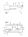
- an electrical circuit 10 in which an electric power semiconductor component 11 is driven by an output stage 12.
- the power semiconductor device 11 may be an insulated gate bipolar transistor (IGBT) or a gate turn-off (GTO) thyristor or the like.
- IGBT insulated gate bipolar transistor
- GTO gate turn-off
- Example becomes in the FIG. 1 the gate G of the power semiconductor device 11 is acted upon by the output stage and further the collector and the emitter are connected to the output stage 12. It is understood that this control can also be designed differently.
- the output stage 12 is in turn connected via two optical waveguides 13, 14 to a controller 15.
- the two optical waveguides 13, 14 are intended to transmit signals in opposite directions. It is understood that instead of the optical waveguides 13, 14, other potential-separating transmission media or transmission types are conceivable, for example via optocouplers or magnetic transmitters or by means of wireless transmissions or the like. It may also be possible to send and receive the electrical signals in both transmission directions via a single transmission medium.
- controller 15 may be provided to further optical fibers with other amplifiers and thus with more Power semiconductor devices to be connected.
- the output stage 12 has a transmitter / receiver 17, to which the two optical waveguides 13, 14 are connected, and which is intended to receive via the optical waveguide 13 incoming light signals and to send on the optical waveguide 14 light signals.
- the transmitter / receiver 17 is connected to a programmable logic 18 and to a processor 19.
- a programmable logic 18 is connected to a programmable logic 18 and to a processor 19.
- FIG. 2 These connections are shown by way of example as simple forward and return lines. It is understood that insofar as other connection options are conceivable, for example, parallel or serial bus structures or the like.
- the logic 18 is provided with an output, with which the gate G of the power semiconductor device 11 is driven. Furthermore, the logic 18 and the processor 19 are connected to each other via a bidirectional line 20. It is understood that this line 20 may be any type of connection, in particular a parallel or serial bus structure.
- the processor 19 may be a conventional microprocessor or signal processor or the like.
- drive signals are sent from the controller 15 via the optical waveguide 14 to the output stage 12. These drive signals are also referred to as "firing pulses FP".
- the drive signals are received by the transmitter / receiver 17 of the power amplifier 12 and processed by the logic 18. From the logic 18, the power semiconductor device 11 is then turned on or off in response to the individual drive signals via its gate G or on or off.
- the drive signals are usually defined signals with predetermined pulse durations and amplitudes. Based on these specifications, the logic 18 can recognize the drive signals and distinguish them from other signals. For this purpose, an upstream filter 21 may be present in the logic 18, from which only the drive signals are passed on for further processing. For example, it is possible that the drive signals have a longer pulse duration, and that the filter 21 does not pass other signals with short signal durations.
- the output stage 12 can detect the switching operations of the power semiconductor component 11 in a manner not shown. Depending on this, the transmitter / receiver 17 of the output stage 12 can send a so-called “indication pulse IP" via the optical waveguide 13 to the controller 15. On the basis of the "indication pulse IP", the controller 15 can conclude the functionality or a malfunction of the power semiconductor component 11.
- the drive signals are also received by the processor 19, but not further processed.
- programming signals are sent to the output stage 12 via the optical waveguide 13 by the controller 10.
- the programming signals are received by the transceiver 17 and forwarded to the logic 18 and the processor 19.
- the programming signals differ in particular with regard to their signal duration and / or amplitude from the drive signals. For example, it is possible that the programming signals have a shorter signal duration.
- the programming signals are therefore filtered out by the filter 21 and not passed on to the logic 18.
- the programming signals are thus not processed by the logic 18 for the purpose of driving the power semiconductor device 11.
- the programming signals are processed by the processor 19.
- the processor 19 can recognize and further process the programming signals transmitted by the control unit as such.
- the transmitted programming signals contain at their beginning in time a start coding, with which the processor 19 is informed that now follow the actual programming signals.
- Programming logic is detected, the logic 18 is switched by the processor 19 via the line 20 from the normal mode in the programming mode. This means that the power semiconductor device 11 is no longer driven by the logic 18 and no other, related to the power semiconductor device 11 functions more of the logic 18 are executed.
- the received programming signals are conditioned by the processor 19 so that the logic 18 can now be programmed with these programming signals.
- JTAG joint test action group.
- FPGAs or CPLDs can be programmed using the JTAG protocol.
- the processed programming signals are passed from the processor 19 via the line 20 to the logic 18.
- the received programming signals are acknowledged by the logic 18 via the same line 20 to the processor 19.
- the logic 18 becomes a function of the programming signals new functionality given. So there is a programming of the logic 18 via the line 20 based on the processed programming signals.
- the end of the programming can be communicated to the processor 19 either by terminating the transmission of the programming signals or by an end coding last transmitted by the control unit 15.
- the logic 18 is switched back from the processor 19 via the line 20 from the programming mode back to the normal mode.
- the end of the programming operation or the return to normal operation can be reported by the processor 19 via the transmitter / receiver 17 to the controller 15.
- a reset signal or the like from the controller 15 is required.
- the logic 18 of the output stage 12 can be reprogrammed.
- other output stages of power semiconductor components can be programmed in a corresponding manner. Overall, it is thus possible, for example, to program all output stages of the power semiconductor components of a converter circuit.
- controller 15 is provided to influence all output stages of the power semiconductor components of an entire power converter circuit, so can from this Control 15 all power amplifiers can also be programmed. If the controller 15 is additionally provided to cooperate with a so-called remote maintenance, it is possible to program the output stages of the converter circuit via this remote maintenance.
Landscapes
- Physics & Mathematics (AREA)
- Mathematical Physics (AREA)
- Engineering & Computer Science (AREA)
- Computer Hardware Design (AREA)
- Computing Systems (AREA)
- General Engineering & Computer Science (AREA)
- Power Engineering (AREA)
- Amplifiers (AREA)
Applications Claiming Priority (1)
| Application Number | Priority Date | Filing Date | Title |
|---|---|---|---|
| DE102010024038A DE102010024038A1 (de) | 2010-06-16 | 2010-06-16 | Verfahren sowie elektrische Schaltung zum Betreiben eines elektrischen Leistungshalbleiter-Bauelements |
Publications (4)
| Publication Number | Publication Date |
|---|---|
| EP2398147A2 true EP2398147A2 (fr) | 2011-12-21 |
| EP2398147A8 EP2398147A8 (fr) | 2012-03-14 |
| EP2398147A3 EP2398147A3 (fr) | 2013-03-13 |
| EP2398147B1 EP2398147B1 (fr) | 2019-09-18 |
Family
ID=45091039
Family Applications (1)
| Application Number | Title | Priority Date | Filing Date |
|---|---|---|---|
| EP11162816.0A Active EP2398147B1 (fr) | 2010-06-16 | 2011-04-18 | Procédé et circuit électrique pour le fonctionnement d'un semi-conducteur de puissance électrique |
Country Status (3)
| Country | Link |
|---|---|
| US (1) | US8583059B2 (fr) |
| EP (1) | EP2398147B1 (fr) |
| DE (1) | DE102010024038A1 (fr) |
Families Citing this family (1)
| Publication number | Priority date | Publication date | Assignee | Title |
|---|---|---|---|---|
| EP3672078A1 (fr) * | 2018-12-18 | 2020-06-24 | Siemens Aktiengesellschaft | Procédé de commande de semi-conducteurs |
Family Cites Families (6)
| Publication number | Priority date | Publication date | Assignee | Title |
|---|---|---|---|---|
| GB2277215B (en) * | 1993-04-16 | 1997-04-23 | Marconi Gec Ltd | A power control switch |
| SE516083C2 (sv) * | 1998-08-12 | 2001-11-12 | Bombardier Transp Gmbh | Anordning för styrning av spännings-laddningsstyrda krafthalvledarelement |
| US7113744B1 (en) * | 1999-10-21 | 2006-09-26 | Broadcom Corporation | Adaptive radio transceiver with a power amplifier |
| US7132868B2 (en) * | 2001-06-27 | 2006-11-07 | Mitsubishi Denki Kabushiki Kaisha | Semiconductor device |
| US7493094B2 (en) * | 2005-01-19 | 2009-02-17 | Micro Mobio Corporation | Multi-mode power amplifier module for wireless communication devices |
| US7138824B1 (en) * | 2004-05-10 | 2006-11-21 | Actel Corporation | Integrated multi-function analog circuit including voltage, current, and temperature monitor and gate-driver circuit blocks |
-
2010
- 2010-06-16 DE DE102010024038A patent/DE102010024038A1/de not_active Ceased
-
2011
- 2011-04-18 EP EP11162816.0A patent/EP2398147B1/fr active Active
- 2011-04-20 US US13/064,836 patent/US8583059B2/en active Active
Non-Patent Citations (1)
| Title |
|---|
| None |
Also Published As
| Publication number | Publication date |
|---|---|
| US8583059B2 (en) | 2013-11-12 |
| EP2398147B1 (fr) | 2019-09-18 |
| US20110309882A1 (en) | 2011-12-22 |
| EP2398147A8 (fr) | 2012-03-14 |
| EP2398147A3 (fr) | 2013-03-13 |
| DE102010024038A1 (de) | 2011-12-22 |
Similar Documents
| Publication | Publication Date | Title |
|---|---|---|
| DE10016712C5 (de) | Sicherheitsschaltgerät und Verfahren zur Einstellung einer Betriebsart eines Sicherheitsschaltgeräts | |
| EP3272467B1 (fr) | Système d'agencement adaptateur | |
| EP1427086B2 (fr) | Appareil électrique et methode pour le faire fonctionner | |
| EP2957074B1 (fr) | Véhicule à moteur équipé d'un bus de communication embarqué et procédé de génération d'informations de bus | |
| EP0106272B1 (fr) | Dispositif d'essai pour circuits électriques d'un véhicule automobile | |
| EP1497558A1 (fr) | Pompe a vide | |
| DE102014006148B4 (de) | Endgerät für ein Automatisierungssystem, Endgeräteanordnung sowie Verfahren zum Betreiben eines Endgeräts für ein Automatisierungssystem | |
| DE102015220297A1 (de) | Abgesetzte Antenneneinrichtung zur Fahrzeug-zu-Fahrzeug (C2C) oder Fahrzeug-zu-X (C2X) Kommunikation | |
| DE2338882A1 (de) | Verfahren und fernwirksystem zum einund ausschalten von elektrischen verbrauchern | |
| EP2398147B1 (fr) | Procédé et circuit électrique pour le fonctionnement d'un semi-conducteur de puissance électrique | |
| DE102018126787B4 (de) | Ladestation für Elektrofahrzeuge mit mindestens zwei Ladeanschlüssen und einer wahlweise auf diese schaltbare Leistungselektronikeinheit | |
| EP3028385B1 (fr) | Agencement pour raccorder un composant à un module de commande maître d'un véhicule | |
| EP0263246B1 (fr) | Multiplexeur protégé contre des explosions | |
| EP3292656B1 (fr) | Électronique de commande pour un véhicule agricole ou forestier | |
| EP1209641B1 (fr) | Procédé de mise en oeuvre d'une installation de télécommande par radio | |
| DE102006017307A1 (de) | Front-End-Modul mit zwei Eingängen zum Entgegennehmen von Sendesignalen | |
| DE3538484A1 (de) | Verfahren zur ueberpruefung von schutzbefehl-uebertragungssystemen im on-line-betrieb | |
| DE102005044620B4 (de) | Front-End-Modul für drahtlose Kommunikationsmittel | |
| EP3706094A1 (fr) | Système comprenant une machine-outil et un appareil auxiliaire ainsi que divers procédés de commande par un interface sans fil | |
| DE102004036489B4 (de) | Schaltung zum Verbinden von wenigstens zwei Signalquellen mit wenigstens einem Signalausgang | |
| EP4391621A1 (fr) | Dispositif de commande sans fil pour un véhicule de transport, en particulier un véhicule de transport modulaire, véhicule de transport équipé d'un tel dispositif de commande et procédé de fonctionnement d'un tel véhicule de transport | |
| DE1588713C3 (de) | Schaltungsanordnung zur selektiven Übertragung von Nachrichten in Fernwirkanlagen zwischen einer Zentrale und einer Vielzahl von Stationen | |
| DE102005009312A1 (de) | Sende-/Empfangsvorrichtung für Sensorsignale und Übertragungssystem zur drahtlosen Übertragung von Sensorsignalen | |
| DE2934039C2 (fr) | ||
| DE102014213569A1 (de) | Fahrzeuggetriebesteuergerät mit mehreren Eingabeschnittstellen für einen Tippschalter |
Legal Events
| Date | Code | Title | Description |
|---|---|---|---|
| AK | Designated contracting states |
Kind code of ref document: A2 Designated state(s): AL AT BE BG CH CY CZ DE DK EE ES FI FR GB GR HR HU IE IS IT LI LT LU LV MC MK MT NL NO PL PT RO RS SE SI SK SM TR |
|
| AX | Request for extension of the european patent |
Extension state: BA ME |
|
| PUAI | Public reference made under article 153(3) epc to a published international application that has entered the european phase |
Free format text: ORIGINAL CODE: 0009012 |
|
| PUAL | Search report despatched |
Free format text: ORIGINAL CODE: 0009013 |
|
| AK | Designated contracting states |
Kind code of ref document: A3 Designated state(s): AL AT BE BG CH CY CZ DE DK EE ES FI FR GB GR HR HU IE IS IT LI LT LU LV MC MK MT NL NO PL PT RO RS SE SI SK SM TR |
|
| AX | Request for extension of the european patent |
Extension state: BA ME |
|
| RIC1 | Information provided on ipc code assigned before grant |
Ipc: H03K 19/177 20060101ALI20130207BHEP Ipc: H03K 17/56 20060101AFI20130207BHEP |
|
| 17P | Request for examination filed |
Effective date: 20130906 |
|
| RAP1 | Party data changed (applicant data changed or rights of an application transferred) |
Owner name: GE ENERGY POWER CONVERSION TECHNOLOGY LIMITED |
|
| RBV | Designated contracting states (corrected) |
Designated state(s): AL AT BE BG CH CY CZ DE DK EE ES FI FR GB GR HR HU IE IS IT LI LT LU LV MC MK MT NL NO PL PT RO RS SE SI SK SM TR |
|
| STAA | Information on the status of an ep patent application or granted ep patent |
Free format text: STATUS: EXAMINATION IS IN PROGRESS |
|
| 17Q | First examination report despatched |
Effective date: 20170221 |
|
| REG | Reference to a national code |
Ref country code: DE Ref legal event code: R079 Ref document number: 502011016101 Country of ref document: DE Free format text: PREVIOUS MAIN CLASS: H03K0017560000 Ipc: H03K0019173000 |
|
| GRAP | Despatch of communication of intention to grant a patent |
Free format text: ORIGINAL CODE: EPIDOSNIGR1 |
|
| STAA | Information on the status of an ep patent application or granted ep patent |
Free format text: STATUS: GRANT OF PATENT IS INTENDED |
|
| RIC1 | Information provided on ipc code assigned before grant |
Ipc: H03K 17/567 20060101ALI20190327BHEP Ipc: H03K 19/173 20060101AFI20190327BHEP Ipc: H03K 17/56 20060101ALI20190327BHEP Ipc: H03F 3/08 20060101ALI20190327BHEP Ipc: H01H 85/041 20060101ALI20190327BHEP Ipc: H01H 85/54 20060101ALI20190327BHEP Ipc: H03K 19/177 20060101ALI20190327BHEP Ipc: H03K 17/687 20060101ALI20190327BHEP |
|
| INTG | Intention to grant announced |
Effective date: 20190423 |
|
| GRAS | Grant fee paid |
Free format text: ORIGINAL CODE: EPIDOSNIGR3 |
|
| GRAA | (expected) grant |
Free format text: ORIGINAL CODE: 0009210 |
|
| STAA | Information on the status of an ep patent application or granted ep patent |
Free format text: STATUS: THE PATENT HAS BEEN GRANTED |
|
| AK | Designated contracting states |
Kind code of ref document: B1 Designated state(s): AL AT BE BG CH CY CZ DE DK EE ES FI FR GB GR HR HU IE IS IT LI LT LU LV MC MK MT NL NO PL PT RO RS SE SI SK SM TR |
|
| REG | Reference to a national code |
Ref country code: GB Ref legal event code: FG4D Free format text: NOT ENGLISH |
|
| REG | Reference to a national code |
Ref country code: CH Ref legal event code: EP |
|
| REG | Reference to a national code |
Ref country code: DE Ref legal event code: R096 Ref document number: 502011016101 Country of ref document: DE |
|
| REG | Reference to a national code |
Ref country code: AT Ref legal event code: REF Ref document number: 1182523 Country of ref document: AT Kind code of ref document: T Effective date: 20191015 |
|
| REG | Reference to a national code |
Ref country code: IE Ref legal event code: FG4D Free format text: LANGUAGE OF EP DOCUMENT: GERMAN |
|
| REG | Reference to a national code |
Ref country code: NL Ref legal event code: MP Effective date: 20190918 |
|
| PG25 | Lapsed in a contracting state [announced via postgrant information from national office to epo] |
Ref country code: BG Free format text: LAPSE BECAUSE OF FAILURE TO SUBMIT A TRANSLATION OF THE DESCRIPTION OR TO PAY THE FEE WITHIN THE PRESCRIBED TIME-LIMIT Effective date: 20191218 Ref country code: SE Free format text: LAPSE BECAUSE OF FAILURE TO SUBMIT A TRANSLATION OF THE DESCRIPTION OR TO PAY THE FEE WITHIN THE PRESCRIBED TIME-LIMIT Effective date: 20190918 Ref country code: HR Free format text: LAPSE BECAUSE OF FAILURE TO SUBMIT A TRANSLATION OF THE DESCRIPTION OR TO PAY THE FEE WITHIN THE PRESCRIBED TIME-LIMIT Effective date: 20190918 Ref country code: LT Free format text: LAPSE BECAUSE OF FAILURE TO SUBMIT A TRANSLATION OF THE DESCRIPTION OR TO PAY THE FEE WITHIN THE PRESCRIBED TIME-LIMIT Effective date: 20190918 Ref country code: FI Free format text: LAPSE BECAUSE OF FAILURE TO SUBMIT A TRANSLATION OF THE DESCRIPTION OR TO PAY THE FEE WITHIN THE PRESCRIBED TIME-LIMIT Effective date: 20190918 Ref country code: NO Free format text: LAPSE BECAUSE OF FAILURE TO SUBMIT A TRANSLATION OF THE DESCRIPTION OR TO PAY THE FEE WITHIN THE PRESCRIBED TIME-LIMIT Effective date: 20191218 |
|
| REG | Reference to a national code |
Ref country code: LT Ref legal event code: MG4D |
|
| PG25 | Lapsed in a contracting state [announced via postgrant information from national office to epo] |
Ref country code: GR Free format text: LAPSE BECAUSE OF FAILURE TO SUBMIT A TRANSLATION OF THE DESCRIPTION OR TO PAY THE FEE WITHIN THE PRESCRIBED TIME-LIMIT Effective date: 20191219 Ref country code: RS Free format text: LAPSE BECAUSE OF FAILURE TO SUBMIT A TRANSLATION OF THE DESCRIPTION OR TO PAY THE FEE WITHIN THE PRESCRIBED TIME-LIMIT Effective date: 20190918 Ref country code: LV Free format text: LAPSE BECAUSE OF FAILURE TO SUBMIT A TRANSLATION OF THE DESCRIPTION OR TO PAY THE FEE WITHIN THE PRESCRIBED TIME-LIMIT Effective date: 20190918 Ref country code: AL Free format text: LAPSE BECAUSE OF FAILURE TO SUBMIT A TRANSLATION OF THE DESCRIPTION OR TO PAY THE FEE WITHIN THE PRESCRIBED TIME-LIMIT Effective date: 20190918 |
|
| PG25 | Lapsed in a contracting state [announced via postgrant information from national office to epo] |
Ref country code: ES Free format text: LAPSE BECAUSE OF FAILURE TO SUBMIT A TRANSLATION OF THE DESCRIPTION OR TO PAY THE FEE WITHIN THE PRESCRIBED TIME-LIMIT Effective date: 20190918 Ref country code: RO Free format text: LAPSE BECAUSE OF FAILURE TO SUBMIT A TRANSLATION OF THE DESCRIPTION OR TO PAY THE FEE WITHIN THE PRESCRIBED TIME-LIMIT Effective date: 20190918 Ref country code: IT Free format text: LAPSE BECAUSE OF FAILURE TO SUBMIT A TRANSLATION OF THE DESCRIPTION OR TO PAY THE FEE WITHIN THE PRESCRIBED TIME-LIMIT Effective date: 20190918 Ref country code: NL Free format text: LAPSE BECAUSE OF FAILURE TO SUBMIT A TRANSLATION OF THE DESCRIPTION OR TO PAY THE FEE WITHIN THE PRESCRIBED TIME-LIMIT Effective date: 20190918 Ref country code: EE Free format text: LAPSE BECAUSE OF FAILURE TO SUBMIT A TRANSLATION OF THE DESCRIPTION OR TO PAY THE FEE WITHIN THE PRESCRIBED TIME-LIMIT Effective date: 20190918 Ref country code: PL Free format text: LAPSE BECAUSE OF FAILURE TO SUBMIT A TRANSLATION OF THE DESCRIPTION OR TO PAY THE FEE WITHIN THE PRESCRIBED TIME-LIMIT Effective date: 20190918 Ref country code: PT Free format text: LAPSE BECAUSE OF FAILURE TO SUBMIT A TRANSLATION OF THE DESCRIPTION OR TO PAY THE FEE WITHIN THE PRESCRIBED TIME-LIMIT Effective date: 20200120 |
|
| PG25 | Lapsed in a contracting state [announced via postgrant information from national office to epo] |
Ref country code: IS Free format text: LAPSE BECAUSE OF FAILURE TO SUBMIT A TRANSLATION OF THE DESCRIPTION OR TO PAY THE FEE WITHIN THE PRESCRIBED TIME-LIMIT Effective date: 20200224 Ref country code: SK Free format text: LAPSE BECAUSE OF FAILURE TO SUBMIT A TRANSLATION OF THE DESCRIPTION OR TO PAY THE FEE WITHIN THE PRESCRIBED TIME-LIMIT Effective date: 20190918 Ref country code: SM Free format text: LAPSE BECAUSE OF FAILURE TO SUBMIT A TRANSLATION OF THE DESCRIPTION OR TO PAY THE FEE WITHIN THE PRESCRIBED TIME-LIMIT Effective date: 20190918 Ref country code: CZ Free format text: LAPSE BECAUSE OF FAILURE TO SUBMIT A TRANSLATION OF THE DESCRIPTION OR TO PAY THE FEE WITHIN THE PRESCRIBED TIME-LIMIT Effective date: 20190918 |
|
| REG | Reference to a national code |
Ref country code: DE Ref legal event code: R097 Ref document number: 502011016101 Country of ref document: DE |
|
| PLBE | No opposition filed within time limit |
Free format text: ORIGINAL CODE: 0009261 |
|
| STAA | Information on the status of an ep patent application or granted ep patent |
Free format text: STATUS: NO OPPOSITION FILED WITHIN TIME LIMIT |
|
| PG2D | Information on lapse in contracting state deleted |
Ref country code: IS |
|
| PG25 | Lapsed in a contracting state [announced via postgrant information from national office to epo] |
Ref country code: DK Free format text: LAPSE BECAUSE OF FAILURE TO SUBMIT A TRANSLATION OF THE DESCRIPTION OR TO PAY THE FEE WITHIN THE PRESCRIBED TIME-LIMIT Effective date: 20190918 Ref country code: IS Free format text: LAPSE BECAUSE OF FAILURE TO SUBMIT A TRANSLATION OF THE DESCRIPTION OR TO PAY THE FEE WITHIN THE PRESCRIBED TIME-LIMIT Effective date: 20200119 |
|
| 26N | No opposition filed |
Effective date: 20200619 |
|
| PG25 | Lapsed in a contracting state [announced via postgrant information from national office to epo] |
Ref country code: SI Free format text: LAPSE BECAUSE OF FAILURE TO SUBMIT A TRANSLATION OF THE DESCRIPTION OR TO PAY THE FEE WITHIN THE PRESCRIBED TIME-LIMIT Effective date: 20190918 |
|
| PG25 | Lapsed in a contracting state [announced via postgrant information from national office to epo] |
Ref country code: MC Free format text: LAPSE BECAUSE OF FAILURE TO SUBMIT A TRANSLATION OF THE DESCRIPTION OR TO PAY THE FEE WITHIN THE PRESCRIBED TIME-LIMIT Effective date: 20190918 |
|
| REG | Reference to a national code |
Ref country code: CH Ref legal event code: PL |
|
| PG25 | Lapsed in a contracting state [announced via postgrant information from national office to epo] |
Ref country code: LI Free format text: LAPSE BECAUSE OF NON-PAYMENT OF DUE FEES Effective date: 20200430 Ref country code: LU Free format text: LAPSE BECAUSE OF NON-PAYMENT OF DUE FEES Effective date: 20200418 Ref country code: CH Free format text: LAPSE BECAUSE OF NON-PAYMENT OF DUE FEES Effective date: 20200430 |
|
| REG | Reference to a national code |
Ref country code: BE Ref legal event code: MM Effective date: 20200430 |
|
| PG25 | Lapsed in a contracting state [announced via postgrant information from national office to epo] |
Ref country code: BE Free format text: LAPSE BECAUSE OF NON-PAYMENT OF DUE FEES Effective date: 20200430 |
|
| PG25 | Lapsed in a contracting state [announced via postgrant information from national office to epo] |
Ref country code: IE Free format text: LAPSE BECAUSE OF NON-PAYMENT OF DUE FEES Effective date: 20200418 |
|
| REG | Reference to a national code |
Ref country code: AT Ref legal event code: MM01 Ref document number: 1182523 Country of ref document: AT Kind code of ref document: T Effective date: 20200418 |
|
| PG25 | Lapsed in a contracting state [announced via postgrant information from national office to epo] |
Ref country code: AT Free format text: LAPSE BECAUSE OF NON-PAYMENT OF DUE FEES Effective date: 20200418 |
|
| PG25 | Lapsed in a contracting state [announced via postgrant information from national office to epo] |
Ref country code: TR Free format text: LAPSE BECAUSE OF FAILURE TO SUBMIT A TRANSLATION OF THE DESCRIPTION OR TO PAY THE FEE WITHIN THE PRESCRIBED TIME-LIMIT Effective date: 20190918 Ref country code: MT Free format text: LAPSE BECAUSE OF FAILURE TO SUBMIT A TRANSLATION OF THE DESCRIPTION OR TO PAY THE FEE WITHIN THE PRESCRIBED TIME-LIMIT Effective date: 20190918 Ref country code: CY Free format text: LAPSE BECAUSE OF FAILURE TO SUBMIT A TRANSLATION OF THE DESCRIPTION OR TO PAY THE FEE WITHIN THE PRESCRIBED TIME-LIMIT Effective date: 20190918 |
|
| PG25 | Lapsed in a contracting state [announced via postgrant information from national office to epo] |
Ref country code: MK Free format text: LAPSE BECAUSE OF FAILURE TO SUBMIT A TRANSLATION OF THE DESCRIPTION OR TO PAY THE FEE WITHIN THE PRESCRIBED TIME-LIMIT Effective date: 20190918 |
|
| PGFP | Annual fee paid to national office [announced via postgrant information from national office to epo] |
Ref country code: DE Payment date: 20250319 Year of fee payment: 15 |
|
| PGFP | Annual fee paid to national office [announced via postgrant information from national office to epo] |
Ref country code: GB Payment date: 20260319 Year of fee payment: 16 |
|
| PGFP | Annual fee paid to national office [announced via postgrant information from national office to epo] |
Ref country code: FR Payment date: 20260319 Year of fee payment: 16 |