EP2395554A2 - Fabrication method for interdigitated back contact photovoltaic cells - Google Patents
Fabrication method for interdigitated back contact photovoltaic cells Download PDFInfo
- Publication number
- EP2395554A2 EP2395554A2 EP11168875A EP11168875A EP2395554A2 EP 2395554 A2 EP2395554 A2 EP 2395554A2 EP 11168875 A EP11168875 A EP 11168875A EP 11168875 A EP11168875 A EP 11168875A EP 2395554 A2 EP2395554 A2 EP 2395554A2
- Authority
- EP
- European Patent Office
- Prior art keywords
- grooves
- layer
- regions
- providing
- doped
- Prior art date
- Legal status (The legal status is an assumption and is not a legal conclusion. Google has not performed a legal analysis and makes no representation as to the accuracy of the status listed.)
- Withdrawn
Links
- 238000000034 method Methods 0.000 title claims abstract description 54
- 238000004519 manufacturing process Methods 0.000 title claims abstract description 10
- 239000000758 substrate Substances 0.000 claims abstract description 70
- 239000002019 doping agent Substances 0.000 claims abstract description 64
- 238000009792 diffusion process Methods 0.000 claims abstract description 19
- 230000000873 masking effect Effects 0.000 claims abstract description 17
- 239000004065 semiconductor Substances 0.000 claims abstract description 14
- 238000002161 passivation Methods 0.000 claims description 12
- 238000000608 laser ablation Methods 0.000 claims description 9
- 239000002184 metal Substances 0.000 claims description 8
- 239000011248 coating agent Substances 0.000 claims description 5
- 238000000576 coating method Methods 0.000 claims description 5
- 238000000151 deposition Methods 0.000 claims description 5
- 230000008021 deposition Effects 0.000 claims description 5
- 238000001465 metallisation Methods 0.000 claims description 5
- 238000001039 wet etching Methods 0.000 claims description 5
- 238000009713 electroplating Methods 0.000 claims description 4
- 238000005468 ion implantation Methods 0.000 claims description 4
- 238000007650 screen-printing Methods 0.000 claims description 3
- 238000001312 dry etching Methods 0.000 claims description 2
- 239000010410 layer Substances 0.000 description 126
- XUIMIQQOPSSXEZ-UHFFFAOYSA-N Silicon Chemical compound [Si] XUIMIQQOPSSXEZ-UHFFFAOYSA-N 0.000 description 18
- 229910052710 silicon Inorganic materials 0.000 description 18
- 239000010703 silicon Substances 0.000 description 18
- 238000005530 etching Methods 0.000 description 13
- HEMHJVSKTPXQMS-UHFFFAOYSA-M Sodium hydroxide Chemical compound [OH-].[Na+] HEMHJVSKTPXQMS-UHFFFAOYSA-M 0.000 description 12
- 239000000463 material Substances 0.000 description 10
- 238000000926 separation method Methods 0.000 description 10
- 229910052581 Si3N4 Inorganic materials 0.000 description 8
- HQVNEWCFYHHQES-UHFFFAOYSA-N silicon nitride Chemical compound N12[Si]34N5[Si]62N3[Si]51N64 HQVNEWCFYHHQES-UHFFFAOYSA-N 0.000 description 8
- BHEPBYXIRTUNPN-UHFFFAOYSA-N hydridophosphorus(.) (triplet) Chemical compound [PH] BHEPBYXIRTUNPN-UHFFFAOYSA-N 0.000 description 6
- ZOXJGFHDIHLPTG-UHFFFAOYSA-N Boron Chemical compound [B] ZOXJGFHDIHLPTG-UHFFFAOYSA-N 0.000 description 4
- 230000015572 biosynthetic process Effects 0.000 description 4
- 229910052796 boron Inorganic materials 0.000 description 4
- 150000004767 nitrides Chemical class 0.000 description 4
- VYPSYNLAJGMNEJ-UHFFFAOYSA-N Silicium dioxide Chemical compound O=[Si]=O VYPSYNLAJGMNEJ-UHFFFAOYSA-N 0.000 description 3
- 238000000708 deep reactive-ion etching Methods 0.000 description 3
- 238000005516 engineering process Methods 0.000 description 3
- 238000002513 implantation Methods 0.000 description 3
- 238000001459 lithography Methods 0.000 description 3
- 229910052814 silicon oxide Inorganic materials 0.000 description 3
- XHXFXVLFKHQFAL-UHFFFAOYSA-N phosphoryl trichloride Chemical compound ClP(Cl)(Cl)=O XHXFXVLFKHQFAL-UHFFFAOYSA-N 0.000 description 2
- 238000007738 vacuum evaporation Methods 0.000 description 2
- 238000003631 wet chemical etching Methods 0.000 description 2
- UFHFLCQGNIYNRP-UHFFFAOYSA-N Hydrogen Chemical compound [H][H] UFHFLCQGNIYNRP-UHFFFAOYSA-N 0.000 description 1
- GRYLNZFGIOXLOG-UHFFFAOYSA-N Nitric acid Chemical compound O[N+]([O-])=O GRYLNZFGIOXLOG-UHFFFAOYSA-N 0.000 description 1
- 229910019213 POCl3 Inorganic materials 0.000 description 1
- PNEYBMLMFCGWSK-UHFFFAOYSA-N aluminium oxide Inorganic materials [O-2].[O-2].[O-2].[Al+3].[Al+3] PNEYBMLMFCGWSK-UHFFFAOYSA-N 0.000 description 1
- 229910021417 amorphous silicon Inorganic materials 0.000 description 1
- 238000003486 chemical etching Methods 0.000 description 1
- 229910052593 corundum Inorganic materials 0.000 description 1
- 230000001419 dependent effect Effects 0.000 description 1
- 229910052732 germanium Inorganic materials 0.000 description 1
- GNPVGFCGXDBREM-UHFFFAOYSA-N germanium atom Chemical compound [Ge] GNPVGFCGXDBREM-UHFFFAOYSA-N 0.000 description 1
- 239000011521 glass Substances 0.000 description 1
- 229910052739 hydrogen Inorganic materials 0.000 description 1
- 239000001257 hydrogen Substances 0.000 description 1
- 238000005286 illumination Methods 0.000 description 1
- 150000002500 ions Chemical class 0.000 description 1
- 229910017604 nitric acid Inorganic materials 0.000 description 1
- 230000008520 organization Effects 0.000 description 1
- 230000003647 oxidation Effects 0.000 description 1
- 238000007254 oxidation reaction Methods 0.000 description 1
- 238000000059 patterning Methods 0.000 description 1
- 238000000206 photolithography Methods 0.000 description 1
- 230000000704 physical effect Effects 0.000 description 1
- 238000001020 plasma etching Methods 0.000 description 1
- 239000002356 single layer Substances 0.000 description 1
- 238000006467 substitution reaction Methods 0.000 description 1
- 229910001845 yogo sapphire Inorganic materials 0.000 description 1
Images


Classifications
-
- H—ELECTRICITY
- H10—SEMICONDUCTOR DEVICES; ELECTRIC SOLID-STATE DEVICES NOT OTHERWISE PROVIDED FOR
- H10F—INORGANIC SEMICONDUCTOR DEVICES SENSITIVE TO INFRARED RADIATION, LIGHT, ELECTROMAGNETIC RADIATION OF SHORTER WAVELENGTH OR CORPUSCULAR RADIATION
- H10F71/00—Manufacture or treatment of devices covered by this subclass
- H10F71/121—The active layers comprising only Group IV materials
-
- H—ELECTRICITY
- H10—SEMICONDUCTOR DEVICES; ELECTRIC SOLID-STATE DEVICES NOT OTHERWISE PROVIDED FOR
- H10F—INORGANIC SEMICONDUCTOR DEVICES SENSITIVE TO INFRARED RADIATION, LIGHT, ELECTROMAGNETIC RADIATION OF SHORTER WAVELENGTH OR CORPUSCULAR RADIATION
- H10F10/00—Individual photovoltaic cells, e.g. solar cells
- H10F10/10—Individual photovoltaic cells, e.g. solar cells having potential barriers
- H10F10/14—Photovoltaic cells having only PN homojunction potential barriers
- H10F10/146—Back-junction photovoltaic cells, e.g. having interdigitated base-emitter regions on the back side
-
- H—ELECTRICITY
- H10—SEMICONDUCTOR DEVICES; ELECTRIC SOLID-STATE DEVICES NOT OTHERWISE PROVIDED FOR
- H10F—INORGANIC SEMICONDUCTOR DEVICES SENSITIVE TO INFRARED RADIATION, LIGHT, ELECTROMAGNETIC RADIATION OF SHORTER WAVELENGTH OR CORPUSCULAR RADIATION
- H10F77/00—Constructional details of devices covered by this subclass
- H10F77/20—Electrodes
- H10F77/206—Electrodes for devices having potential barriers
- H10F77/211—Electrodes for devices having potential barriers for photovoltaic cells
- H10F77/219—Arrangements for electrodes of back-contact photovoltaic cells
-
- Y—GENERAL TAGGING OF NEW TECHNOLOGICAL DEVELOPMENTS; GENERAL TAGGING OF CROSS-SECTIONAL TECHNOLOGIES SPANNING OVER SEVERAL SECTIONS OF THE IPC; TECHNICAL SUBJECTS COVERED BY FORMER USPC CROSS-REFERENCE ART COLLECTIONS [XRACs] AND DIGESTS
- Y02—TECHNOLOGIES OR APPLICATIONS FOR MITIGATION OR ADAPTATION AGAINST CLIMATE CHANGE
- Y02E—REDUCTION OF GREENHOUSE GAS [GHG] EMISSIONS, RELATED TO ENERGY GENERATION, TRANSMISSION OR DISTRIBUTION
- Y02E10/00—Energy generation through renewable energy sources
- Y02E10/50—Photovoltaic [PV] energy
- Y02E10/547—Monocrystalline silicon PV cells
-
- Y—GENERAL TAGGING OF NEW TECHNOLOGICAL DEVELOPMENTS; GENERAL TAGGING OF CROSS-SECTIONAL TECHNOLOGIES SPANNING OVER SEVERAL SECTIONS OF THE IPC; TECHNICAL SUBJECTS COVERED BY FORMER USPC CROSS-REFERENCE ART COLLECTIONS [XRACs] AND DIGESTS
- Y02—TECHNOLOGIES OR APPLICATIONS FOR MITIGATION OR ADAPTATION AGAINST CLIMATE CHANGE
- Y02P—CLIMATE CHANGE MITIGATION TECHNOLOGIES IN THE PRODUCTION OR PROCESSING OF GOODS
- Y02P70/00—Climate change mitigation technologies in the production process for final industrial or consumer products
- Y02P70/50—Manufacturing or production processes characterised by the final manufactured product
Definitions
- the present invention relates to methods for fabrication of interdigitated back contact photovoltaic cells.
- Interdigitated back contact (IBC) cells are photovoltaic cells having both emitter contacts and base contacts at the rear side of the cells, the emitter contacts and base contacts being interdigitated for separate collection of electrons and holes. Eliminating front side contacts avoids the need for making a trade-off between shading losses and series resistance. Fabrication processes for IBC cells often require several masking steps and alignment steps, because at the rear side of the cells there is a need for separating emitter regions and base regions and for separating and properly aligning emitter contacts and base contacts.
- a window is opened in the oxide layer and the nitride layer at the bottom of the grooves.
- the silicon oxide layer and the silicon nitride layer remain at the sidewalls of the grooves.
- a boron pre-deposition is then performed and both doping regions (n+ emitter region and p+ region in the base) are diffused in a single high temperature step.
- the silicon oxide / silicon nitride stack present at the sidewalls of the grooves is used as a masking layer.
- an Al layer is deposited by vacuum evaporation which features a very poor step coverage, such that the presence of the cantilevers leads to a separation between emitter contacts and base contacts.
- Embodiments of the present invention relate to a method for manufacturing interdigitated back contact photovoltaic cells wherein the need for lithography steps and the need for alignment steps are avoided, and wherein the number of process steps is reduced as compared to prior art processes.
- the need for providing a masking layer for separating n-type doped regions and p-type doped regions is avoided.
- a combination of providing cantilevers or overhanging parts at the sides of grooves etched in a silicon substrate and directional doping is used for the separation between n-type doped regions and p-type doped regions. Diffusion of dopants for forming an emitter, a back surface field and a front surface field can be performed in a single step.
- the cantilevers can also be used for separation between emitter contacts and base contacts, such that a single metallisation step can be used for forming both contact types.
- the present invention relates to a method for fabricating interdigitated back contact photovoltaic cells, the method comprising: providing on a rear surface of a semiconductor, e.g. silicon, substrate a first doped layer comprising a first dopant type; providing a dielectric masking layer overlaying the first doped layer; forming a plurality of grooves through the dielectric masking layer and the first doped layer, the plurality of grooves extending into the silicon in a direction substantially orthogonal, e.g. orthogonal, to the rear surface and extending in a lateral direction underneath the first doped layer at sides of the plurality of grooves; performing a directional doping step in a direction substantially orthogonal, e.g.
- substantially orthogonal to the rear surface in the context of the present invention is meant deviating not more than 30°, preferably not more than 10° from an orthogonal to the rear surface.
- the doped regions of the first type and the doped regions of the second type are 'self-aligned', i.e. there is no need for providing a dedicated mask or masking layer for separating the doped regions of the first type from the doped regions of the second type.
- the substrate can for example be an n-type substrate, the first dopant type can be n-type and the second dopant type can be p-type.
- the dopant diffusion step may comprise forming n-type regions (e.g. back surface field regions) in between the plurality of grooves and p-type regions (e.g. emitter regions) at the bottom of the plurality of grooves.
- the substrate can for example be an n-type substrate
- the first dopant type can be p-type
- the second dopant type can be n-type
- the dopant diffusion step may comprise forming p-type regions (e.g. emitter regions) in between the plurality of grooves and n-type regions (e.g. back surface field regions) at the bottom of the plurality of grooves.
- the substrate can for example be a p-type substrate, the first dopant type can be p-type and the second dopant type can be n-type.
- the dopant diffusion step may comprise forming p-type regions (e.g. back surface field regions) in between the plurality of grooves and n-type regions (e.g. emitter regions) at the bottom of the plurality of grooves.
- the substrate can for example be a p-type substrate
- the first dopant type can be n-type
- the second dopant type can be p-type.
- the dopant diffusion step may comprise forming n-type regions (e.g. emitter regions) in between the plurality of grooves and p-type regions (e.g. back surface field regions) at the bottom of the plurality of grooves.
- the first doped layer can for example be a doped oxide layer or a doped amorphous semiconductor layer, e.g. amorphous silicon layer.
- the dielectric masking layer can be a single layer or a stack of layers.
- the dielectric masking layer can include any suitable dielectric layer, such as for example an oxide layer and/or a nitride layer.
- Forming the plurality of grooves can for example be done by laser ablation, followed by wet etching for underetching the dielectric masking layer and the first doped layer, the wet etching step resulting in an extension of the grooves in a lateral direction (i.e. a direction substantially parallel to the rear surface) underneath the first doped layer.
- Wet etching can for example comprise etching in any suitable wet etching solution, e.g. a NaOH solution or a KOH solution. The etching solution may be dependent on the substrate.
- dry etching can be used (e.g. DRIE: deep reactive ion etching) or screenprinting of a paste that selectively etches dielectric layers.
- the plurality of grooves can for example be parallel grooves, e.g. having a rectangular shape in a plane parallel to the substrate surface.
- the depth (i.e. the size in a direction orthogonal to the substrate surface) of the grooves can for example be in the range between about 1 micrometer and 5 micrometer and the lateral size (in a direction parallel to the substrate surface) can for example be in the range between about 40 micrometer and 2 mm, for example in the range between about 100 micrometer and 1 mm, for example in the order of about 300 micrometer.
- the pitch between the grooves can for example be in the range between about 60 micrometer and 3 mm.
- the grooves extend in a lateral direction underneath the first doped layer at sides of the plurality of grooves.
- the first doped layer (and the dielectric layer overlaying the first doped layer) comprises an overhanging part or a cantilever.
- the lateral size of this overhanging part can for example be in the range between about 1 micrometer and 5 micrometer.
- Performing a directional doping step can comprise performing an ion implantation step, a plasma doping step, or a suitable low pressure deposition step, e.g. at sub-atmospheric pressures, with high anisotropy.
- anisotropy is meant the circumstance that the value of a physical property of the doping step has different values depending on the direction in which it is considered, and is notas in the case of isotropy--the same when considered in every spatial direction.
- concentration-related parameters are particularly interest in this context.
- the method may further comprise providing, before the dopant diffusion step, a second doped layer at a front side of the substrate, the second doped layer having the same dopant type as the substrate.
- the dopant diffusion step then results also in the formation of a doped region at the front side of the silicon substrate, for example providing a Front Side Field in the photovoltaic cell.
- the method can further comprise providing a surface passivation layer at the front side and at the rear side of the substrate, providing an antireflection coating at the front side, and providing emitter contacts and base contacts at the rear side.
- Providing emitter contacts and base contacts can for example comprise providing openings through the different layers present at the rear side, for example by laser ablation, to locally expose the doped regions of the first type and the doped regions of the second type.
- a thin metal seed layer can be provided, followed by electroplating.
- emitter contacts and base contacts can be provided by vacuum evaporation, wherein the presence of cantilevers may lead to a separation of both contact types.
- a method according to embodiments of the present invention may be based on laser patterning, which is a clean technology, on underetching and on ion-implantation.
- the front surface or front side of a photovoltaic cell is the surface or side adapted for being oriented towards a light source and thus for receiving illumination.
- the back surface, back side, rear surface or rear side of a photovoltaic cell is the surface or side opposite to the front surface.
- the front side of a substrate is the side of the substrate corresponding to the front side of the photovoltaic cell to be fabricated, while the rear side or back side of the substrate corresponds to the back side of the photovoltaic cell to be fabricated.
- interdigitated means intermingled, whereby items from one group and items from another group are alternately presented.
- the interdigitation relates to the back contacts of a photovoltaic cell. Advantages of such interdigitated back contacts are a lack of grid shading loss.
- a method for fabricating interdigitated back contact photovoltaic cells comprises: providing on a rear surface of a semiconductor, e.g. silicon, substrate a first doped layer comprising a first dopant type; providing a dielectric masking layer overlaying the first doped layer; forming a plurality of grooves through the dielectric masking layer and the first doped layer, the plurality of grooves extending into the semiconductor substrate in a direction substantially orthogonal, e.g.
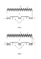
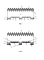
- FIG. 1 to FIG.8 An example of a fabrication process for IBC photovoltaic cells in accordance with a method according to one embodiment is illustrated in FIG. 1 to FIG.8 .
- the method is illustrated for an exemplary embodiment wherein a semiconductor substrate comprising dopants of a first dopant type, e.g. an n-type silicon substrate, is used.
- the doping concentration of the semiconductor substrate 10 may for example be such that the resistivity of the substrate is in the range between 0.5 and 10 Ohm-cm.
- the method is not limited thereto and can also be used for fabricating photovoltaic cells on substrates of another semiconductor material, e.g. germanium substrates, and/or of another dopant type, e.g. p-type substrates and/or other dopant concentrations hence other resistivities.
- a first doped layer e.g. a first oxide layer 11 comprising a dopant of the first type, e.g. an n-type dopant, such as for example a phosphorous doped oxide layer
- the thickness of the first doped layer 11 may be in the range between 20 nm and 200 nm.
- the dopant concentration of the first doped layer 11 may be in the range between 1e18/cm 3 and 5e20/cm 3 .
- an n-type dopant such as for example a phosphorous doped oxide layer
- the thickness of the second doped layer 12 may be in the range between 20 nm and 200 nm. In embodiments of the present invention, the dopant concentration of the second doped layer 12 may be in the range between 1e18/cm 3 and 5e20/cm 3 .
- the first and second doped layers, e.g. the phosphorous doped oxide layers 11, 12, can for example be a POCl3 glass, a phosphorous doped CVD oxide or any other suitable doped oxide layer known to a person skilled in the art.
- the first doped oxide layer 11 and the second doped oxide layer 12 can be provided simultaneously, e.g. in one oxidation step.
- other suitable types of doped layers known to a person skilled in the art can be used such as for example an ion implanted silicon layer.
- a dielectric layer or a dielectric layer stack 13 is provided at the rear side of the substrate 10, the dielectric layer stack 13 overlaying the first doped layer, e.g. oxide layer 11.
- the dielectric layer stack 13 can for example comprise a deposited silicon oxide layer (e.g. having a thickness in the range between about 50 nm and 1 micrometer), and/or a silicon nitride layer (e.g. having a thickness in the range between about 50 nm and 500 nm, e.g. having a thickness in the range between about 50 nm and 150 nm, e.g., having a thickness of about 100 nm).
- the dielectric layer stack 13 at the rear side may comprise a material for passivation, e.g. a silicon nitride layer, that may be used as a hydrogen source to passivate the rear surface of the photovoltaic cell. In addition, it may provide a protection from the metal that is provided in a later stage of the process when forming the electrodes. In other embodiments of the present invention a rear surface passivation layer or layer stack can be provided in a later stage of the process. In such embodiments all layers present at the rear side of the substrate (first doped layer 11 and, if present, dielectric layer stack 13) can be removed after performing the dopant diffusion step, and a rear side passivation layer or layer stack can be provided afterwards.
- a material for passivation e.g. a silicon nitride layer
- an additional layer such as a silicon nitride layer 14 can be provided on the second doped oxide layer 12.
- the silicon nitride layer 14 can function as an antireflection coating in the final photovoltaic cell structure. Therefore, the thickness of the silicon nitride layer 14 is preferably in the range between about 50 nm and 150 nm.
- an antireflection coating can be provided in a later stage of the process, for example after performing the dopant diffusion step.
- the second doped layer 12 may be removed and a surface passivation layer may be provided after performing the dopant diffusion step and before providing an antireflection coating.
- a plurality of grooves 17 is formed in the substrate material, e.g. silicon ( FIG. 3 ), at the rear side of the substrate 10 at locations where emitter regions will be formed in a later stage of the process.
- the plurality of grooves 17 can for example be formed by laser ablation.
- the grooves 17 have a shape corresponding to the shape of the emitter region to be formed in a later stage of the process.
- the grooves can have a substantially rectangular shape, for example a rectangular shape, in a cross-section according to a plane parallel to the substrate rear surface, having the length of the photovoltaic cell to be formed and having a width W for example in the range between about 40 micrometer and 2 mm, for example in the range between about 100 micrometer and 1 mm, for example in the order of about 300 micrometer.
- the pitch P between the grooves can for example be in the range between about 60 micrometer and 3 mm.
- the depth of the grooves is larger than the depth of the back surface field to be formed in a later stage of the process. The final depth d of the grooves (shown in FIG.
- the actual depth of the grooves 17 within the substrate material can for example be in the range between about 500 nm and 10 micrometer, e.g. between about 1 micrometer and 5 micrometer.
- other methods known to a person skilled in the art can be used, such as for example lithography and DRIE etching or screenprinting an etching paste for etching the dielectric layers, followed by etching the grooves in the substrate material, e.g. silicon.
- a wet chemical etching is performed, e.g. with a NaOH-based or a KOH-based etching solution, using the dielectric layer 13 as a masking layer.
- the NaOH (or KOH) based etching solution may for example comprise about 100 g to 200 g NaOH (or KOH) per 1 liter of H 2 O and etching may be performed at a temperature of about 85oC or less.
- suitable etching solutions known to a person skilled in the art can be used, such as for example a HNO 3 +BHF+H 2O based etching solution.
- the etching solution is selected such that the substrate material has a faster etch rate than the overlying layers 11, 13 at the rear side.
- the wet chemical etching step removes damage that may be caused in the substrate material, e.g. silicon, by the laser ablation step, and creates underetching due to the faster etch rate of the substrate, e.g. silicon substrate 10, as compared to the etch rate of the dielectric layer 13 and first doped layer, e.g. oxide layer 11. This results in a structure as shown in FIG. 4 . Due to the underetching, at the sides of the grooves 17 overhanging parts or cantilevers are formed by the first doped layer, e.g. oxide layer 11, and the dielectric layer 13.
- the width W o of the overhanging parts, or thus the depth of the underetching can for example be in the range between about 1 micrometer and 5 micrometer.
- a directional doping step with dopants of a second type e.g. p-type dopants, such as for example a Boron implantation step
- dopants of a second type e.g. p-type dopants, such as for example a Boron implantation step
- doped regions 18 comprising a dopant of the second type, e.g. p-type dopant such as Boron, are formed at the rear side of the substrate 10 at a bottom of the plurality of grooves 17, where emitter regions are to be formed.
- the presence of the cantilevers at the sides of the grooves 17 leads, later on, to a separation between the emitter regions to be formed (using the doped regions 18 as a dopant source) at the bottom of the grooves and the back surface field (BSF) regions to be formed (using the first doped oxide layer 11 as a dopant source) in between the grooves 17.
- BSF back surface field
- other directional doping steps than ion implantation can be used, such as for example plasma doping or any other directional doping step known by a person skilled in the art.
- a high temperature step is performed, for example during about 5 to 10 minutes at a temperature in the range between about 1000oC and 1050oC, leading (in a single step) to the diffusion of second type dopants, e.g. boron from doped regions 18, into the substrate material, e.g. silicon, in the grooves at the rear side of the substrate 10, thereby forming emitter regions 20; to the diffusion of first type dopants, e.g. phosphorous from the first doped layer, e.g. oxide layer 11, into the substrate material, e.g. silicon, at the rear side of the substrate surface in between grooves 17, thereby forming back surface field regions 21; and leading to the diffusion of first type dopants, e.g.
- second type dopants e.g. boron from doped regions 18, into the substrate material, e.g. silicon, in the grooves at the rear side of the substrate 10, thereby forming emitter regions 20
- first type dopants e.g. phosphorous from the first do
- the second doped layer e.g. oxide layer 12 at the front side, thereby forming front surface field regions 22 at the textured front surface of the photovoltaic cell. Due to the presence of cantilevers at the sides of the grooves 17, this process leads to a good separation between regions of the first dopant type, e.g. n+ regions (BSF regions 21), and regions of the second dopant type, e.g. p+ regions (emitter regions 20), at the rear side, without the need for providing masking layers e.g. at the sidewalls of the grooves.
- the resulting structure is shown in FIG. 6 .
- the surface passivation layer 23 is provided at the rear side of the structure, more in particular at the exposed substrate surface, e.g. silicon surface, of the grooves 17 ( FIG. 7 ).
- the surface passivation layer 23 can for example be a stack comprising a thermal oxide (e.g. having a thickness in the range between about 3 nm and 10 nm) and a deposited oxide or nitride or a stack comprising an Al 2 O 3 layer (e.g. with a thickness in the order of about 30 nm) and a deposited oxide layer or nitride layer, or any other layer or stack of layers suitable for passivation, and known to a person skilled in the art.
- a thermal oxide e.g. having a thickness in the range between about 3 nm and 10 nm
- a deposited oxide or nitride e.g. with a thickness in the order of about 30 nm
- Al 2 O 3 layer e.g. with a thickness in the order of
- the different layers previously provided on the substrate 10 can be removed after the dopant diffusion step, followed by providing a surface passivation layer over the entire rear (and front) surface of the substrate 10.
- a further process step comprises forming openings, for example by laser ablation, through the layers at the rear side, up to the doped semiconductor substrate material, e.g. silicon, to enable the formation of metal point contacts to the emitter regions 20 and the BSF regions 21. Openings are made through the surface passivation layer 23 such that the emitter regions 20 are locally exposed. Openings are also provided through the stack of layers in between the grooves 17 (first doped oxide layer 11, dielectric layer 13 in the example shown) such that the, in the embodiment illustrated, n+ doped BSF regions 21 are locally exposed.
- metal contacts are provided through the openings formed through the layers covering the rear side of the semiconductor, e.g. silicon, substrate 10, more in particular emitter contacts 24 to the emitter regions 20 and base contacts 25 to the BSF regions 21 ( FIG. 8 ).
- the emitter contacts 24 and the base contacts 25 are preferably interdigitated and can for example be comb-shaped.
- the metallization for forming both contact types can be done in a single process. Electrode separation between emitter contacts 24 and base contacts 25 can be obtained because of the presence of the grooves 17, leading to a metal discontinuity at the edges of the grooves.
- Metallization can for example be done by deposition of a seed layer, e.g. an about 100 nm thick seed layer comprising a Ti/Cu stack, followed by electroplating (e.g. about 4 micrometer thick Cu electroplating), or by deposition of a metal layer (for example an about 1 micrometer thick Al layer).
- FIG. 1 to FIG. 8 illustrate a process sequence wherein emitter regions are formed at the bottom of the plurality of grooves and BSF regions are formed in between the grooves
- the present invention is not limited thereto.
- a method can also be used for fabricating IBC cells wherein BSF regions are formed at the bottom of the grooves and wherein emitter regions are formed in between the grooves.
Landscapes
- Photovoltaic Devices (AREA)
- Life Sciences & Earth Sciences (AREA)
- Engineering & Computer Science (AREA)
- Sustainable Development (AREA)
- Sustainable Energy (AREA)
Abstract
providing a dielectric masking layer (13) overlaying the first doped layer (11),
forming a plurality of grooves (17) through the dielectric masking layer (13) and the first doped layer (11), the plurality of grooves (17) extending into the semiconductor substrate (10) in a direction substantially orthogonal to the rear surface and extending in a lateral direction underneath the first doped layer (11) at sides of the plurality of grooves (17),
performing a directional doping step in a direction substantially orthogonal to the rear surface,
thereby providing doped regions (18) with dopants of a second dopant type different from the first dopant type at a bottom of the plurality of grooves (17),
performing a dopant diffusion step, thereby forming at the rear side of the substrate (10) either one of emitter regions (20) or back surface field regions (21) in between the plurality of grooves and the other one of emitter regions (20) or back surface field regions (21) at the bottom of the plurality of grooves.
Description
- The present invention relates to methods for fabrication of interdigitated back contact photovoltaic cells.
- Interdigitated back contact (IBC) cells are photovoltaic cells having both emitter contacts and base contacts at the rear side of the cells, the emitter contacts and base contacts being interdigitated for separate collection of electrons and holes. Eliminating front side contacts avoids the need for making a trade-off between shading losses and series resistance. Fabrication processes for IBC cells often require several masking steps and alignment steps, because at the rear side of the cells there is a need for separating emitter regions and base regions and for separating and properly aligning emitter contacts and base contacts.
- Methods have been proposed for reducing the complexity of process sequences for manufacturing IBC cells. For example, in "Realization of self-aligned back contact cells", Electrochemical and Solid-State Letters, 11 (5), H114-H117, 2008, P. Papet et al describe a process sequence wherein only one lithography step is used and wherein no alignment steps are needed afterwards. Separation between emitter contacts and base contacts is obtained by chemical etching of grooves in a silicon substrate using a metal mask, wherein underetching of the mask leads to the formation of cantilevers, the cantilevers being sufficiently large (a few micrometers) to avoid short circuits between both contact types after metal deposition.
- In "Super self-aligned technology for backside contact solar cells: a route to low cost and high efficiency", IEEE PVSC 2009, P. Verlinden et al propose a method for fabricating backside contact photovoltaic cells, the method requiring only one photolithography step without alignment. Separation between n+ doped regions and p+ doped regions at the rear side of the cells is obtained by chemically etching grooves in the silicon substrate using an oxide mask and underetching the mask such that oxide cantilevers are formed at the sides of the grooves. The bottom and the sidewalls of the grooves are thermally oxidized to provide a passivation layer, and a silicon nitride layer is deposited on top of the oxide layer. Next, using anisotropic Reactive Ion Etching, and using the cantilevers as a mask, a window is opened in the oxide layer and the nitride layer at the bottom of the grooves. The silicon oxide layer and the silicon nitride layer remain at the sidewalls of the grooves. A boron pre-deposition is then performed and both doping regions (n+ emitter region and p+ region in the base) are diffused in a single high temperature step. In order to provide a separation between n+ doped regions and p+ doped regions, the silicon oxide / silicon nitride stack present at the sidewalls of the grooves is used as a masking layer. For forming emitter contacts and base contacts, an Al layer is deposited by vacuum evaporation which features a very poor step coverage, such that the presence of the cantilevers leads to a separation between emitter contacts and base contacts.
- It is an object of embodiments of the present invention to provide a good method for manufacturing solar cells with both contacts at the rear.
- The above objective is accomplished by a method according to embodiments of the present invention.
- Embodiments of the present invention relate to a method for manufacturing interdigitated back contact photovoltaic cells wherein the need for lithography steps and the need for alignment steps are avoided, and wherein the number of process steps is reduced as compared to prior art processes. In a method according to one embodiment, the need for providing a masking layer for separating n-type doped regions and p-type doped regions is avoided. A combination of providing cantilevers or overhanging parts at the sides of grooves etched in a silicon substrate and directional doping is used for the separation between n-type doped regions and p-type doped regions. Diffusion of dopants for forming an emitter, a back surface field and a front surface field can be performed in a single step. In addition, the cantilevers can also be used for separation between emitter contacts and base contacts, such that a single metallisation step can be used for forming both contact types.
- In a first embodiment, the present invention relates to a method for fabricating interdigitated back contact photovoltaic cells, the method comprising: providing on a rear surface of a semiconductor, e.g. silicon, substrate a first doped layer comprising a first dopant type; providing a dielectric masking layer overlaying the first doped layer; forming a plurality of grooves through the dielectric masking layer and the first doped layer, the plurality of grooves extending into the silicon in a direction substantially orthogonal, e.g. orthogonal, to the rear surface and extending in a lateral direction underneath the first doped layer at sides of the plurality of grooves; performing a directional doping step in a direction substantially orthogonal, e.g. orthogonal, to the rear surface, thereby providing dopants of a second dopant type different from the first dopant type at a bottom of the plurality of grooves; performing a dopant diffusion step, thereby forming at the rear side of the substrate doped regions of a first type in between the plurality of grooves and doped regions of a second type at the bottom of the plurality of grooves. With "substantially orthogonal to the rear surface" in the context of the present invention is meant deviating not more than 30°, preferably not more than 10° from an orthogonal to the rear surface.
- It is an advantage of embodiments of the present invention that the doped regions of the first type and the doped regions of the second type are 'self-aligned', i.e. there is no need for providing a dedicated mask or masking layer for separating the doped regions of the first type from the doped regions of the second type.
- It is an advantage of embodiments of the present invention that the back surface field and the emitter are produced simultaneously. This provides a simplified way of processing solar cells.
- In embodiments or the present invention, the substrate can for example be an n-type substrate, the first dopant type can be n-type and the second dopant type can be p-type. In such embodiment the dopant diffusion step may comprise forming n-type regions (e.g. back surface field regions) in between the plurality of grooves and p-type regions (e.g. emitter regions) at the bottom of the plurality of grooves.
- Alternatively, in embodiments of the present invention, the substrate can for example be an n-type substrate, the first dopant type can be p-type and the second dopant type can be n-type. In such embodiment the dopant diffusion step may comprise forming p-type regions (e.g. emitter regions) in between the plurality of grooves and n-type regions (e.g. back surface field regions) at the bottom of the plurality of grooves.
- Alternatively, in embodiments of the present invention, the substrate can for example be a p-type substrate, the first dopant type can be p-type and the second dopant type can be n-type. In such embodiment the dopant diffusion step may comprise forming p-type regions (e.g. back surface field regions) in between the plurality of grooves and n-type regions (e.g. emitter regions) at the bottom of the plurality of grooves.
- Alternatively, in embodiments of the present invention, the substrate can for example be a p-type substrate, the first dopant type can be n-type and the second dopant type can be p-type. In such embodiment the dopant diffusion step may comprise forming n-type regions (e.g. emitter regions) in between the plurality of grooves and p-type regions (e.g. back surface field regions) at the bottom of the plurality of grooves.
- The first doped layer can for example be a doped oxide layer or a doped amorphous semiconductor layer, e.g. amorphous silicon layer.
- The dielectric masking layer can be a single layer or a stack of layers. The dielectric masking layer can include any suitable dielectric layer, such as for example an oxide layer and/or a nitride layer.
- Forming the plurality of grooves can for example be done by laser ablation, followed by wet etching for underetching the dielectric masking layer and the first doped layer, the wet etching step resulting in an extension of the grooves in a lateral direction (i.e. a direction substantially parallel to the rear surface) underneath the first doped layer. Wet etching can for example comprise etching in any suitable wet etching solution, e.g. a NaOH solution or a KOH solution. The etching solution may be dependent on the substrate. As an alternative to laser ablation, for example dry etching can be used (e.g. DRIE: deep reactive ion etching) or screenprinting of a paste that selectively etches dielectric layers.
- The plurality of grooves can for example be parallel grooves, e.g. having a rectangular shape in a plane parallel to the substrate surface.
- The depth (i.e. the size in a direction orthogonal to the substrate surface) of the grooves can for example be in the range between about 1 micrometer and 5 micrometer and the lateral size (in a direction parallel to the substrate surface) can for example be in the range between about 40 micrometer and 2 mm, for example in the range between about 100 micrometer and 1 mm, for example in the order of about 300 micrometer. The pitch between the grooves can for example be in the range between about 60 micrometer and 3 mm.
- In one embodiment the grooves extend in a lateral direction underneath the first doped layer at sides of the plurality of grooves. In other words, at the sides of the plurality of grooves the first doped layer (and the dielectric layer overlaying the first doped layer) comprises an overhanging part or a cantilever. The lateral size of this overhanging part can for example be in the range between about 1 micrometer and 5 micrometer.
- Performing a directional doping step can comprise performing an ion implantation step, a plasma doping step, or a suitable low pressure deposition step, e.g. at sub-atmospheric pressures, with high anisotropy. By anisotropy is meant the circumstance that the value of a physical property of the doping step has different values depending on the direction in which it is considered, and is notas in the case of isotropy--the same when considered in every spatial direction. Of particular interest in this context are concentration-related parameters.
- In one embodiment, the method may further comprise providing, before the dopant diffusion step, a second doped layer at a front side of the substrate, the second doped layer having the same dopant type as the substrate. The dopant diffusion step then results also in the formation of a doped region at the front side of the silicon substrate, for example providing a Front Side Field in the photovoltaic cell.
- In one embodiment, the method can further comprise providing a surface passivation layer at the front side and at the rear side of the substrate, providing an antireflection coating at the front side, and providing emitter contacts and base contacts at the rear side.
- Providing emitter contacts and base contacts can for example comprise providing openings through the different layers present at the rear side, for example by laser ablation, to locally expose the doped regions of the first type and the doped regions of the second type. Next a thin metal seed layer can be provided, followed by electroplating. Alternatively, emitter contacts and base contacts can be provided by vacuum evaporation, wherein the presence of cantilevers may lead to a separation of both contact types.
- It is an advantage of a manufacturing method according to embodiments of the present invention that it is litho-free. A method according to embodiments of the present invention may be based on laser patterning, which is a clean technology, on underetching and on ion-implantation.
- For purposes of illustration, certain objects and advantages of the invention have been described herein above. Of course, it is to be understood that not necessarily all such objects or advantages may be achieved in accordance with any particular embodiment of the invention. Thus, for example, those skilled in the art will recognize that the invention may be embodied or carried out in a manner that achieves or optimizes one advantage or group of advantages as taught herein without necessarily achieving other objects or advantages as may be taught or suggested herein. Further, it is understood that this summary is merely an example and is not intended to limit the scope of the invention. The invention, both as to organization and method of operation, together with features and advantages thereof, may best be understood by reference to the following detailed description when read in conjunction with the accompanying drawings.
-
-
FIG. 1 to FIG. 8 schematically illustrate an exemplary method according to an embodiment of the present invention. - In the different drawings, the same reference signs refer to the same or analogous elements.
- In the following detailed description, numerous specific details are set forth in order to provide a thorough understanding of the invention and how it may be practiced in particular embodiments. However, it will be understood that the present invention may be practiced without these specific details. In other instances, well-known methods, procedures and techniques have not been described in detail, so as not to obscure the present disclosure. While the present invention will be described with respect to particular embodiments and with reference to certain drawings, the invention is not limited hereto. The drawings included and described herein are schematic and are not limiting the scope of the invention. It is also noted that in the drawings, the size of some elements may be exaggerated and, therefore, not drawn to scale for illustrative purposes.
- Furthermore, the terms first, second, third and the like in the description and in the claims, are used for distinguishing between similar elements and not necessarily for describing a sequence, either temporally, spatially, in ranking or in any other manner. It is to be understood that the terms so used are interchangeable under appropriate circumstances and that the embodiments of the invention described herein are capable of operation in other sequences than described or illustrated herein.
- Moreover, the terms top, bottom, over, under and the like in the description and in the claims are used for descriptive purposes and not necessarily for describing relative positions. It is to be understood that the terms so used are interchangeable under appropriate circumstances and that the embodiments of the invention described herein are capable of operation in other orientations than described or illustrated herein.
- It is to be noticed that the term "comprising" should not be interpreted as being restricted to the means listed thereafter; it does not exclude other elements or steps. It is thus to be interpreted as specifying the presence of the stated features, integers, steps or components as referred to, but does not preclude the presence or addition of one or more other features, integers, steps or components, or groups thereof. Thus, the scope of the expression "a device comprising means A and B" should not be limited to devices consisting only of components A and B.
- In the context of the present invention, the front surface or front side of a photovoltaic cell is the surface or side adapted for being oriented towards a light source and thus for receiving illumination. The back surface, back side, rear surface or rear side of a photovoltaic cell is the surface or side opposite to the front surface. The front side of a substrate is the side of the substrate corresponding to the front side of the photovoltaic cell to be fabricated, while the rear side or back side of the substrate corresponds to the back side of the photovoltaic cell to be fabricated.
- In the context of the present invention, interdigitated means intermingled, whereby items from one group and items from another group are alternately presented. In particular, the interdigitation relates to the back contacts of a photovoltaic cell. Advantages of such interdigitated back contacts are a lack of grid shading loss.
- A method for fabricating interdigitated back contact photovoltaic cells according to one embodiment of the present invention comprises: providing on a rear surface of a semiconductor, e.g. silicon, substrate a first doped layer comprising a first dopant type; providing a dielectric masking layer overlaying the first doped layer; forming a plurality of grooves through the dielectric masking layer and the first doped layer, the plurality of grooves extending into the semiconductor substrate in a direction substantially orthogonal, e.g. orthogonal, to the rear surface of the semiconductor substrate and extending in a lateral direction underneath the first doped layer at sides of the plurality of grooves; performing a directional doping step in a direction substantially orthogonal to the rear surface, thereby providing doped regions with dopants of a second dopant type different from the first dopant type at a bottom of the plurality of grooves; performing a dopant diffusion step, thereby forming at the rear side of the substrate doped regions of a first type in between the plurality of grooves and doped regions of a second type at the bottom of the plurality of grooves.
- An example of a fabrication process for IBC photovoltaic cells in accordance with a method according to one embodiment is illustrated in
FIG. 1 to FIG.8 . The method is illustrated for an exemplary embodiment wherein a semiconductor substrate comprising dopants of a first dopant type, e.g. an n-type silicon substrate, is used. The doping concentration of thesemiconductor substrate 10 may for example be such that the resistivity of the substrate is in the range between 0.5 and 10 Ohm-cm. However, the method is not limited thereto and can also be used for fabricating photovoltaic cells on substrates of another semiconductor material, e.g. germanium substrates, and/or of another dopant type, e.g. p-type substrates and/or other dopant concentrations hence other resistivities. - After texturing the front side of an n-
type substrate 10, a first doped layer, e.g. afirst oxide layer 11 comprising a dopant of the first type, e.g. an n-type dopant, such as for example a phosphorous doped oxide layer, is provided at the rear side of the substrate (FIG. 1 ). The thickness of the first dopedlayer 11 may be in the range between 20 nm and 200 nm. In embodiments of the present invention, the dopant concentration of the first dopedlayer 11 may be in the range between 1e18/cm3 and 5e20/cm3. A second doped layer, e.g. a seconddoped oxide layer 12 comprising a dopant of the first type, e.g. an n-type dopant, such as for example a phosphorous doped oxide layer, can be provided at the front side of thesubstrate 10. The thickness of the second dopedlayer 12 may be in the range between 20 nm and 200 nm. In embodiments of the present invention, the dopant concentration of the second dopedlayer 12 may be in the range between 1e18/cm3 and 5e20/cm3. The first and second doped layers, e.g. the phosphorous doped oxide layers 11, 12, can for example be a POCl3 glass, a phosphorous doped CVD oxide or any other suitable doped oxide layer known to a person skilled in the art. The firstdoped oxide layer 11 and the seconddoped oxide layer 12 can be provided simultaneously, e.g. in one oxidation step. As an alternative to a doped oxide layer, other suitable types of doped layers known to a person skilled in the art can be used such as for example an ion implanted silicon layer. - Next, as illustrated in
FIG. 2 , a dielectric layer or adielectric layer stack 13, is provided at the rear side of thesubstrate 10, thedielectric layer stack 13 overlaying the first doped layer,e.g. oxide layer 11. Thedielectric layer stack 13 can for example comprise a deposited silicon oxide layer (e.g. having a thickness in the range between about 50 nm and 1 micrometer), and/or a silicon nitride layer (e.g. having a thickness in the range between about 50 nm and 500 nm, e.g. having a thickness in the range between about 50 nm and 150 nm, e.g., having a thickness of about 100 nm). - The
dielectric layer stack 13 at the rear side may comprise a material for passivation, e.g. a silicon nitride layer, that may be used as a hydrogen source to passivate the rear surface of the photovoltaic cell. In addition, it may provide a protection from the metal that is provided in a later stage of the process when forming the electrodes. In other embodiments of the present invention a rear surface passivation layer or layer stack can be provided in a later stage of the process. In such embodiments all layers present at the rear side of the substrate (first dopedlayer 11 and, if present, dielectric layer stack 13) can be removed after performing the dopant diffusion step, and a rear side passivation layer or layer stack can be provided afterwards. - At the front side, an additional layer such as a
silicon nitride layer 14 can be provided on the seconddoped oxide layer 12. Thesilicon nitride layer 14 can function as an antireflection coating in the final photovoltaic cell structure. Therefore, the thickness of thesilicon nitride layer 14 is preferably in the range between about 50 nm and 150 nm. However, in other embodiments of the present invention, an antireflection coating can be provided in a later stage of the process, for example after performing the dopant diffusion step. In such embodiments the second dopedlayer 12 may be removed and a surface passivation layer may be provided after performing the dopant diffusion step and before providing an antireflection coating. - In a next step, a plurality of
grooves 17 is formed in the substrate material, e.g. silicon (FIG. 3 ), at the rear side of thesubstrate 10 at locations where emitter regions will be formed in a later stage of the process. The plurality ofgrooves 17 can for example be formed by laser ablation. Thegrooves 17 have a shape corresponding to the shape of the emitter region to be formed in a later stage of the process. For example, the grooves can have a substantially rectangular shape, for example a rectangular shape, in a cross-section according to a plane parallel to the substrate rear surface, having the length of the photovoltaic cell to be formed and having a width W for example in the range between about 40 micrometer and 2 mm, for example in the range between about 100 micrometer and 1 mm, for example in the order of about 300 micrometer. The pitch P between the grooves can for example be in the range between about 60 micrometer and 3 mm. The depth of the grooves is larger than the depth of the back surface field to be formed in a later stage of the process. The final depth d of the grooves (shown inFIG. 4 , the actual depth of thegrooves 17 within the substrate material) can for example be in the range between about 500 nm and 10 micrometer, e.g. between about 1 micrometer and 5 micrometer. As an alternative to laser ablation for the formation ofgrooves 17, other methods known to a person skilled in the art can be used, such as for example lithography and DRIE etching or screenprinting an etching paste for etching the dielectric layers, followed by etching the grooves in the substrate material, e.g. silicon. - After laser ablation, a wet chemical etching is performed, e.g. with a NaOH-based or a KOH-based etching solution, using the
dielectric layer 13 as a masking layer. The NaOH (or KOH) based etching solution may for example comprise about 100 g to 200 g NaOH (or KOH) per 1 liter of H2O and etching may be performed at a temperature of about 85ºC or less. However, in a method according to one embodiment, other suitable etching solutions known to a person skilled in the art can be used, such as for example a HNO3+BHF+H2O based etching solution. The etching solution is selected such that the substrate material has a faster etch rate than the overlying layers 11, 13 at the rear side. The wet chemical etching step removes damage that may be caused in the substrate material, e.g. silicon, by the laser ablation step, and creates underetching due to the faster etch rate of the substrate,e.g. silicon substrate 10, as compared to the etch rate of thedielectric layer 13 and first doped layer,e.g. oxide layer 11. This results in a structure as shown inFIG. 4 . Due to the underetching, at the sides of thegrooves 17 overhanging parts or cantilevers are formed by the first doped layer,e.g. oxide layer 11, and thedielectric layer 13. The width Wo of the overhanging parts, or thus the depth of the underetching, can for example be in the range between about 1 micrometer and 5 micrometer. - In a next step, illustrated in
FIG. 5 , a directional doping step with dopants of a second type, e.g. p-type dopants, such as for example a Boron implantation step, is performed at the rear side of thesubstrate 10, in a direction substantially orthogonal, e.g. orthogonal, to the plane of the rear surface. As a result of the doping step, e.g. implantation step, dopedregions 18 comprising a dopant of the second type, e.g. p-type dopant such as Boron, are formed at the rear side of thesubstrate 10 at a bottom of the plurality ofgrooves 17, where emitter regions are to be formed. As implantation is a highly directional step, the presence of the cantilevers at the sides of thegrooves 17 leads, later on, to a separation between the emitter regions to be formed (using the dopedregions 18 as a dopant source) at the bottom of the grooves and the back surface field (BSF) regions to be formed (using the firstdoped oxide layer 11 as a dopant source) in between thegrooves 17. In embodiments of the present invention, other directional doping steps than ion implantation can be used, such as for example plasma doping or any other directional doping step known by a person skilled in the art. - Next a high temperature step is performed, for example during about 5 to 10 minutes at a temperature in the range between about 1000ºC and 1050ºC, leading (in a single step) to the diffusion of second type dopants, e.g. boron from
doped regions 18, into the substrate material, e.g. silicon, in the grooves at the rear side of thesubstrate 10, thereby formingemitter regions 20; to the diffusion of first type dopants, e.g. phosphorous from the first doped layer,e.g. oxide layer 11, into the substrate material, e.g. silicon, at the rear side of the substrate surface in betweengrooves 17, thereby forming backsurface field regions 21; and leading to the diffusion of first type dopants, e.g. phosphorous, from the second doped layer,e.g. oxide layer 12 at the front side, thereby forming frontsurface field regions 22 at the textured front surface of the photovoltaic cell. Due to the presence of cantilevers at the sides of thegrooves 17, this process leads to a good separation between regions of the first dopant type, e.g. n+ regions (BSF regions 21), and regions of the second dopant type, e.g. p+ regions (emitter regions 20), at the rear side, without the need for providing masking layers e.g. at the sidewalls of the grooves. The resulting structure is shown inFIG. 6 . - Next a
surface passivation layer 23 is provided at the rear side of the structure, more in particular at the exposed substrate surface, e.g. silicon surface, of the grooves 17 (FIG. 7 ). Thesurface passivation layer 23 can for example be a stack comprising a thermal oxide (e.g. having a thickness in the range between about 3 nm and 10 nm) and a deposited oxide or nitride or a stack comprising an Al2O3 layer (e.g. with a thickness in the order of about 30 nm) and a deposited oxide layer or nitride layer, or any other layer or stack of layers suitable for passivation, and known to a person skilled in the art. - In alternative embodiments of the present invention (not illustrated in the drawings), the different layers previously provided on the substrate 10 (
dielectric layer 13, first dopedlayer 11, second doped layer 12) can be removed after the dopant diffusion step, followed by providing a surface passivation layer over the entire rear (and front) surface of thesubstrate 10. - A further process step comprises forming openings, for example by laser ablation, through the layers at the rear side, up to the doped semiconductor substrate material, e.g. silicon, to enable the formation of metal point contacts to the
emitter regions 20 and theBSF regions 21. Openings are made through thesurface passivation layer 23 such that theemitter regions 20 are locally exposed. Openings are also provided through the stack of layers in between the grooves 17 (first dopedoxide layer 11,dielectric layer 13 in the example shown) such that the, in the embodiment illustrated, n+ dopedBSF regions 21 are locally exposed. - Finally metal contacts are provided through the openings formed through the layers covering the rear side of the semiconductor, e.g. silicon,
substrate 10, more inparticular emitter contacts 24 to theemitter regions 20 andbase contacts 25 to the BSF regions 21 (FIG. 8 ). Theemitter contacts 24 and thebase contacts 25 are preferably interdigitated and can for example be comb-shaped. The metallization for forming both contact types can be done in a single process. Electrode separation betweenemitter contacts 24 andbase contacts 25 can be obtained because of the presence of thegrooves 17, leading to a metal discontinuity at the edges of the grooves. Metallization can for example be done by deposition of a seed layer, e.g. an about 100 nm thick seed layer comprising a Ti/Cu stack, followed by electroplating (e.g. about 4 micrometer thick Cu electroplating), or by deposition of a metal layer (for example an about 1 micrometer thick Al layer). - Although
FIG. 1 to FIG. 8 illustrate a process sequence wherein emitter regions are formed at the bottom of the plurality of grooves and BSF regions are formed in between the grooves, the present invention is not limited thereto. For example, a method can also be used for fabricating IBC cells wherein BSF regions are formed at the bottom of the grooves and wherein emitter regions are formed in between the grooves. - The foregoing description details certain embodiments of the invention. It will be appreciated, however, that no matter how detailed the foregoing appears in text, the invention may be practiced in many ways. It should be noted that the use of particular terminology when describing certain features or aspects of the invention should not be taken to imply that the terminology is being re-defined herein to be restricted to including any specific characteristics of the features or aspects of the invention with which that terminology is associated.
- While the above detailed description has shown, described, and pointed out novel features of the invention as applied to various embodiments, it will be understood that various omissions, substitutions, and changes in the form and details of the device or process illustrated may be made by those skilled in the technology without departing from the spirit of the invention.
Claims (10)
- A method for manufacturing interdigitated back contact photovoltaic cells, comprising providing on a rear surface of a semiconductor substrate (10) a first doped layer (11) comprising a first dopant type,
providing a dielectric masking layer (13) overlaying the first doped layer (11),
forming a plurality of grooves (17) through the dielectric masking layer (13) and the first doped layer (11), the plurality of grooves (17) extending into the semiconductor substrate (10) in a direction substantially orthogonal to the rear surface and extending in a lateral direction underneath the first doped layer (11) at sides of the plurality of grooves (17),
performing a directional doping step in a direction substantially orthogonal to the rear surface, thereby providing doped regions (18) with dopants of a second dopant type different from the first dopant type at a bottom of the plurality of grooves (17),
performing a dopant diffusion step, thereby forming at the rear side of the substrate (10) either one of emitter regions (20) or back surface field regions (21) in between the plurality of grooves and the other one of emitter regions (20) or back surface field regions (21) at the bottom of the plurality of grooves. - A method according to claim 1, wherein forming a plurality of grooves (17) comprises forming grooves (16) by means of laser ablation, followed by a wet etching of the formed grooves (16).
- A method according to claim 1, wherein forming a plurality of grooves (17) includes performing a dry etching step.
- A method according to claim 1, wherein forming a plurality of grooves (17) includes screenprinting onto the substrate (10) a paste that selectively etches dielectric layers (11, 13).
- A method according to any of the previous claims, wherein performing a directional doping step comprises performing any of an ion implantation step, a plasma doping step, a low pressure deposition step with high anisotropy.
- A method according to any of the previous claims, furthermore comprising providing, before the dopant diffusion step, a second doped layer (12) at a front side of the substrate (10), the second doped layer (12) having dopants of a same dopant type as the substrate (10).
- A method according to any of the previous claims, furthermore comprising providing one or more of a surface passivation layer (14) at the front side and/or the rear side of the substrate (10), an antireflection coating at the front side or providing emitter contacts and base contacts at the rear side.
- A method according to claim 7, wherein providing emitter contacts and base contacts comprises
providing openings through the different layers present at the rear side to locally expose the doped regions of the first type and the doped regions of the second type, and providing the emitter and base contacts onto the doped regions of the first and the second type. - A method according to claim 8, furthermore comprising providing a metal seed layer before electroplating the emitter and base contacts.
- A method according to any of claims 8 or 9, wherein providing emitter contacts and base contacts is performed in a single metallization step.
Applications Claiming Priority (1)
| Application Number | Priority Date | Filing Date | Title |
|---|---|---|---|
| US35463410P | 2010-06-14 | 2010-06-14 |
Publications (2)
| Publication Number | Publication Date |
|---|---|
| EP2395554A2 true EP2395554A2 (en) | 2011-12-14 |
| EP2395554A3 EP2395554A3 (en) | 2015-03-11 |
Family
ID=44118285
Family Applications (1)
| Application Number | Title | Priority Date | Filing Date |
|---|---|---|---|
| EP11168875.0A Withdrawn EP2395554A3 (en) | 2010-06-14 | 2011-06-07 | Fabrication method for interdigitated back contact photovoltaic cells |
Country Status (4)
| Country | Link |
|---|---|
| US (1) | US8900891B2 (en) |
| EP (1) | EP2395554A3 (en) |
| JP (1) | JP5608609B2 (en) |
| TW (1) | TWI515916B (en) |
Cited By (7)
| Publication number | Priority date | Publication date | Assignee | Title |
|---|---|---|---|---|
| EP2634815A1 (en) * | 2012-03-02 | 2013-09-04 | Samsung SDI Co., Ltd. | Back-contact solar cell and fabrication method thereof |
| WO2013152971A1 (en) * | 2012-04-12 | 2013-10-17 | Robert Bosch Gmbh | Method for producing a thin layer solar module |
| EP2791976A1 (en) * | 2011-12-16 | 2014-10-22 | International Solar Energy Research Center Konstanz E.V. | Back-contact solar cell and method for producing a back-contact solar cell |
| EP2804219B1 (en) * | 2013-05-16 | 2019-10-16 | LG Electronics, Inc. | Solar cell and method for manufacturing the same |
| CN113299771A (en) * | 2021-06-04 | 2021-08-24 | 浙江爱旭太阳能科技有限公司 | Solar cell with buried selective contact region and back contact structure thereof |
| US12278295B1 (en) | 2023-10-13 | 2025-04-15 | Zhejiang Jinko Solar Co., Ltd. | Solar cell, method for manufacturing solar cell, and photovoltaic module |
| EP4539129A1 (en) * | 2023-10-13 | 2025-04-16 | Zhejiang Jinko Solar Co., Ltd. | Solar cell and photovoltaic module |
Families Citing this family (51)
| Publication number | Priority date | Publication date | Assignee | Title |
|---|---|---|---|---|
| US9318644B2 (en) * | 2009-05-05 | 2016-04-19 | Solexel, Inc. | Ion implantation and annealing for thin film crystalline solar cells |
| JP5485062B2 (en) * | 2010-07-30 | 2014-05-07 | 三洋電機株式会社 | Solar cell manufacturing method and solar cell |
| EP2740157B1 (en) * | 2011-08-04 | 2015-04-29 | Imec | Interdigitated electrode formation |
| US8664015B2 (en) * | 2011-10-13 | 2014-03-04 | Samsung Sdi Co., Ltd. | Method of manufacturing photoelectric device |
| US9018517B2 (en) * | 2011-11-07 | 2015-04-28 | International Business Machines Corporation | Silicon heterojunction photovoltaic device with wide band gap emitter |
| KR20130062775A (en) * | 2011-12-05 | 2013-06-13 | 엘지전자 주식회사 | Solar cell and method for manufacturing the same |
| US8637948B2 (en) * | 2012-01-10 | 2014-01-28 | Samsung Sdi Co., Ltd. | Photovoltaic device |
| US8766090B2 (en) | 2012-03-19 | 2014-07-01 | Rec Solar Pte. Ltd. | Method for metallization or metallization and interconnection of back contact solar cells |
| MY184055A (en) * | 2012-05-29 | 2021-03-17 | Solexel Inc | Structures and methods of formation of contiguous and non-contiguous base regions for high efficiency back-contact solar cells |
| TWI455335B (en) * | 2012-06-26 | 2014-10-01 | Motech Ind Inc | Back-contact solar cell and method of manufacturing the same |
| US9209102B2 (en) | 2012-06-29 | 2015-12-08 | Taiwan Semiconductor Manufacturing Company, Ltd. | Passivation structure and method of making the same |
| US8884405B2 (en) * | 2012-06-29 | 2014-11-11 | Taiwan Semiconductor Manufacturing Company, Ltd. | Passivation scheme |
| KR101977927B1 (en) * | 2012-07-11 | 2019-05-13 | 인텔렉츄얼 키스톤 테크놀로지 엘엘씨 | Photoelectric device and the manufacturing method thereof |
| US9515217B2 (en) | 2012-11-05 | 2016-12-06 | Solexel, Inc. | Monolithically isled back contact back junction solar cells |
| WO2014071417A2 (en) * | 2012-11-05 | 2014-05-08 | Solexel, Inc. | Systems and methods for monolithically isled solar photovoltaic cells and modules |
| CN103872185B (en) * | 2012-12-18 | 2016-06-29 | 国际商业机器公司 | Interdigital back contacts photovoltaic device of field effect and forming method thereof |
| KR102044466B1 (en) * | 2013-01-16 | 2019-11-13 | 엘지전자 주식회사 | Solar cell and manufacturing method thereof |
| US9859455B2 (en) | 2013-02-08 | 2018-01-02 | International Business Machines Corporation | Interdigitated back contact heterojunction photovoltaic device with a floating junction front surface field |
| US9640699B2 (en) | 2013-02-08 | 2017-05-02 | International Business Machines Corporation | Interdigitated back contact heterojunction photovoltaic device |
| TW201432925A (en) * | 2013-02-08 | 2014-08-16 | Ind Tech Res Inst | Twin crystal solar cell structure |
| KR20150119262A (en) * | 2013-02-12 | 2015-10-23 | 솔렉셀, 인크. | Monolithically isled back contact back junction solar cells using bulk wafers |
| US8574951B1 (en) * | 2013-02-20 | 2013-11-05 | National Tsing Hua University | Process of manufacturing an interdigitated back-contact solar cell |
| US8901010B2 (en) * | 2013-03-15 | 2014-12-02 | Sunpower Corporation | Methods for improving solar cell lifetime and efficiency |
| JPWO2014163043A1 (en) * | 2013-04-02 | 2017-02-16 | シャープ株式会社 | Photoelectric conversion element |
| WO2014163042A1 (en) * | 2013-04-02 | 2014-10-09 | シャープ株式会社 | Photoelectric conversion element |
| KR101997922B1 (en) * | 2013-04-18 | 2019-07-08 | 엘지전자 주식회사 | Solar cell and manufacturing method thereof |
| KR102045001B1 (en) * | 2013-06-05 | 2019-12-02 | 엘지전자 주식회사 | Solar cell and method for manufacturing the same |
| US20150221792A1 (en) * | 2013-12-23 | 2015-08-06 | Solexel, Inc. | Self Aligned Contacts for Solar Cells |
| US20150270421A1 (en) * | 2014-03-20 | 2015-09-24 | Varian Semiconductor Equipment Associates, Inc. | Advanced Back Contact Solar Cells |
| JP2015191962A (en) * | 2014-03-27 | 2015-11-02 | 三菱電機株式会社 | Solar cell and method for manufacturing the same |
| US9947812B2 (en) * | 2014-03-28 | 2018-04-17 | Sunpower Corporation | Metallization of solar cells |
| US9455368B2 (en) * | 2014-07-03 | 2016-09-27 | Varian Semiconductor Equipment Associates, Inc. | Method of forming an interdigitated back contact solar cell |
| KR101630061B1 (en) * | 2014-09-15 | 2016-06-13 | 엘지전자 주식회사 | Solar cell |
| US9837576B2 (en) | 2014-09-19 | 2017-12-05 | Sunpower Corporation | Solar cell emitter region fabrication with differentiated P-type and N-type architectures and incorporating dotted diffusion |
| FR3026563A1 (en) * | 2014-09-29 | 2016-04-01 | Commissariat Energie Atomique | PROCESS FOR PRODUCING A PHOTOVOLTAIC CELL HOMOJUNCTION |
| WO2016152022A1 (en) * | 2015-03-24 | 2016-09-29 | パナソニックIpマネジメント株式会社 | Method for manufacturing solar cell |
| US12046687B2 (en) | 2016-10-25 | 2024-07-23 | Shin-Etsu Chemical Co., Ltd. | Solar cell with high photoelectric conversion efficiency and method for manufacturing solar cell with high photoelectric conversion efficiency |
| CN109906515A (en) * | 2016-10-25 | 2019-06-18 | 信越化学工业株式会社 | High photoelectric conversion efficiency solar cell and method for manufacturing high photoelectric conversion efficiency solar cell |
| NL2017872B1 (en) * | 2016-11-25 | 2018-06-08 | Stichting Energieonderzoek Centrum Nederland | Photovoltaic cell with passivating contact |
| JP2019161052A (en) * | 2018-03-14 | 2019-09-19 | 国立研究開発法人産業技術総合研究所 | Solar cell and method for manufacturing the same |
| US12132136B2 (en) | 2019-04-03 | 2024-10-29 | Alliance For Sustainable Energy, Llc | CdSeTe photovoltaic devices with interdigitated back contact architecture |
| CN110112256A (en) * | 2019-04-29 | 2019-08-09 | 国家电投集团西安太阳能电力有限公司 | Dry-method slotting method for back contact battery |
| CN114695577A (en) * | 2020-12-30 | 2022-07-01 | 浙江爱旭太阳能科技有限公司 | Back junction back contact solar cell of P-type silicon substrate and manufacturing method thereof |
| WO2023041177A1 (en) * | 2021-09-17 | 2023-03-23 | Universität Konstanz | Doping of a silicon substrate by laser doping with a subsequent high-temperature step |
| CN116741849A (en) * | 2022-06-08 | 2023-09-12 | 浙江晶科能源有限公司 | A kind of solar cell and photovoltaic component |
| KR20240158332A (en) * | 2022-09-08 | 2024-11-04 | 쟝쑤 리드마이크로 나노 테크놀러지 컴퍼니 리미티드 | Charge storage structure and method for manufacturing the same |
| JP7389934B1 (en) | 2023-03-16 | 2023-11-30 | 浙江愛旭太陽能科技有限公司 | Back contact solar cells, back contact solar cell assemblies and solar power generation systems |
| DE102023130440B3 (en) * | 2023-11-03 | 2025-03-06 | EnPV GmbH | Back-side contacted solar cell and method for producing a back-side contacted solar cell |
| CN118969870A (en) * | 2024-01-26 | 2024-11-15 | 隆基绿能科技股份有限公司 | Back contact battery and manufacturing method thereof |
| CN117637874B (en) * | 2024-01-26 | 2024-06-21 | 隆基绿能科技股份有限公司 | Back contact battery and manufacturing method thereof |
| CN117712212B (en) * | 2024-02-05 | 2024-04-23 | 天合光能股份有限公司 | Solar cell and method for manufacturing solar cell |
Family Cites Families (10)
| Publication number | Priority date | Publication date | Assignee | Title |
|---|---|---|---|---|
| US5053083A (en) | 1989-05-08 | 1991-10-01 | The Board Of Trustees Of The Leland Stanford Junior University | Bilevel contact solar cells |
| DE19819200B4 (en) * | 1998-04-29 | 2006-01-05 | Fraunhofer-Gesellschaft zur Förderung der angewandten Forschung e.V. | Solar cell with contact structures and method for producing the contact structures |
| US7388147B2 (en) * | 2003-04-10 | 2008-06-17 | Sunpower Corporation | Metal contact structure for solar cell and method of manufacture |
| KR20080091105A (en) * | 2005-11-24 | 2008-10-09 | 뉴사우스 이노베이션즈 피티와이 리미티드 | High efficiency solar cell manufacturing |
| WO2009029900A1 (en) | 2007-08-31 | 2009-03-05 | Applied Materials, Inc. | Improved methods of emitter formation in solar cells |
| US7517709B1 (en) | 2007-11-16 | 2009-04-14 | Applied Materials, Inc. | Method of forming backside point contact structures for silicon solar cells |
| US20090227095A1 (en) | 2008-03-05 | 2009-09-10 | Nicholas Bateman | Counterdoping for solar cells |
| US7851698B2 (en) | 2008-06-12 | 2010-12-14 | Sunpower Corporation | Trench process and structure for backside contact solar cells with polysilicon doped regions |
| US7999175B2 (en) * | 2008-09-09 | 2011-08-16 | Palo Alto Research Center Incorporated | Interdigitated back contact silicon solar cells with laser ablated grooves |
| US8187979B2 (en) * | 2009-12-23 | 2012-05-29 | Varian Semiconductor Equipment Associates, Inc. | Workpiece patterning with plasma sheath modulation |
-
2011
- 2011-06-07 EP EP11168875.0A patent/EP2395554A3/en not_active Withdrawn
- 2011-06-09 TW TW100120103A patent/TWI515916B/en not_active IP Right Cessation
- 2011-06-14 US US13/160,434 patent/US8900891B2/en not_active Expired - Fee Related
- 2011-06-14 JP JP2011131830A patent/JP5608609B2/en not_active Expired - Fee Related
Non-Patent Citations (2)
| Title |
|---|
| P. PAPET: "Realization of self-aligned back contact cells", ELECTROCHEMICAL AND SOLID-STATE LETTERS, vol. 11, no. 5, 2008, pages H114 - H117 |
| P. VERLINDEN: "Super self-aligned technology for backside contact solar cells: a route to low cost and high efficiency", IEEE PVSC, 2009 |
Cited By (9)
| Publication number | Priority date | Publication date | Assignee | Title |
|---|---|---|---|---|
| EP2791976A1 (en) * | 2011-12-16 | 2014-10-22 | International Solar Energy Research Center Konstanz E.V. | Back-contact solar cell and method for producing a back-contact solar cell |
| EP2634815A1 (en) * | 2012-03-02 | 2013-09-04 | Samsung SDI Co., Ltd. | Back-contact solar cell and fabrication method thereof |
| US9312405B2 (en) | 2012-03-02 | 2016-04-12 | Intellectual Keystone Technology Llc | Thin film type solar cell and fabrication method thereof |
| WO2013152971A1 (en) * | 2012-04-12 | 2013-10-17 | Robert Bosch Gmbh | Method for producing a thin layer solar module |
| EP2804219B1 (en) * | 2013-05-16 | 2019-10-16 | LG Electronics, Inc. | Solar cell and method for manufacturing the same |
| CN113299771A (en) * | 2021-06-04 | 2021-08-24 | 浙江爱旭太阳能科技有限公司 | Solar cell with buried selective contact region and back contact structure thereof |
| US12278295B1 (en) | 2023-10-13 | 2025-04-15 | Zhejiang Jinko Solar Co., Ltd. | Solar cell, method for manufacturing solar cell, and photovoltaic module |
| EP4539129A1 (en) * | 2023-10-13 | 2025-04-16 | Zhejiang Jinko Solar Co., Ltd. | Solar cell and photovoltaic module |
| US12376415B2 (en) | 2023-10-13 | 2025-07-29 | Zhejiang Jinko Solar Co., Ltd. | Solar cell and photovoltaic module |
Also Published As
| Publication number | Publication date |
|---|---|
| US20110303280A1 (en) | 2011-12-15 |
| US8900891B2 (en) | 2014-12-02 |
| TW201203594A (en) | 2012-01-16 |
| EP2395554A3 (en) | 2015-03-11 |
| TWI515916B (en) | 2016-01-01 |
| JP2012004565A (en) | 2012-01-05 |
| JP5608609B2 (en) | 2014-10-15 |
Similar Documents
| Publication | Publication Date | Title |
|---|---|---|
| US8900891B2 (en) | Fabrication method for interdigitated back contact photovoltaic cells | |
| CN202601572U (en) | back contact sheet battery | |
| US9337380B2 (en) | Method for fabricating heterojunction interdigitated back contact photovoltaic cells | |
| CN100401532C (en) | Solar cell and manufacturing method thereof | |
| US9564551B2 (en) | Method of manufacturing a hybrid emitter all back contact solar cell | |
| EP2702614B1 (en) | Method of forming emitters for a back-contact solar cell | |
| CN106057934B (en) | Back contact solar cell device | |
| EP2462622B1 (en) | Methods and apparatus for metallization of solar cells | |
| CN102160192B (en) | Method for fabricating solar cell using direct-pattern pin-hole-free masking layer | |
| US20140073081A1 (en) | Solar Cell Having Selective Emitter | |
| CN106252457A (en) | Mixed type polysilicon hetero-junctions back contact battery | |
| US9496430B2 (en) | Method for forming patterns of differently doped regions | |
| Vitanov et al. | Fabrication of buried contact silicon solar cells using porous silicon | |
| US20130122641A1 (en) | Method of Fabricating Buried Contacts of Solar Cell with Curved Trenches | |
| TWI578549B (en) | Optoelectronic element and solar cell employing the same | |
| KR20130073916A (en) | Photovoltaic cell comprising a region suspended by a conductive pattern and production process | |
| US20170012149A1 (en) | High efficiency single crystal silicon solar cell with epitaxially deposited silicon layers with deep junction(s) | |
| TWI566424B (en) | Optoelectronic element and solar cell employing the same | |
| CN121285053A (en) | Solar cell and preparation method thereof |
Legal Events
| Date | Code | Title | Description |
|---|---|---|---|
| AK | Designated contracting states |
Kind code of ref document: A2 Designated state(s): AL AT BE BG CH CY CZ DE DK EE ES FI FR GB GR HR HU IE IS IT LI LT LU LV MC MK MT NL NO PL PT RO RS SE SI SK SM TR |
|
| AX | Request for extension of the european patent |
Extension state: BA ME |
|
| PUAI | Public reference made under article 153(3) epc to a published international application that has entered the european phase |
Free format text: ORIGINAL CODE: 0009012 |
|
| PUAL | Search report despatched |
Free format text: ORIGINAL CODE: 0009013 |
|
| AK | Designated contracting states |
Kind code of ref document: A3 Designated state(s): AL AT BE BG CH CY CZ DE DK EE ES FI FR GB GR HR HU IE IS IT LI LT LU LV MC MK MT NL NO PL PT RO RS SE SI SK SM TR |
|
| AX | Request for extension of the european patent |
Extension state: BA ME |
|
| RIC1 | Information provided on ipc code assigned before grant |
Ipc: H01L 31/0224 20060101ALI20150205BHEP Ipc: H01L 31/068 20120101AFI20150205BHEP Ipc: H01L 31/18 20060101ALI20150205BHEP |
|
| 17P | Request for examination filed |
Effective date: 20150911 |
|
| RBV | Designated contracting states (corrected) |
Designated state(s): AL AT BE BG CH CY CZ DE DK EE ES FI FR GB GR HR HU IE IS IT LI LT LU LV MC MK MT NL NO PL PT RO RS SE SI SK SM TR |
|
| RAP1 | Party data changed (applicant data changed or rights of an application transferred) |
Owner name: IMEC VZW |
|
| STAA | Information on the status of an ep patent application or granted ep patent |
Free format text: STATUS: THE APPLICATION HAS BEEN WITHDRAWN |
|
| 18W | Application withdrawn |
Effective date: 20190621 |