EP2395553A2 - Solarzelle - Google Patents
Solarzelle Download PDFInfo
- Publication number
- EP2395553A2 EP2395553A2 EP10015635A EP10015635A EP2395553A2 EP 2395553 A2 EP2395553 A2 EP 2395553A2 EP 10015635 A EP10015635 A EP 10015635A EP 10015635 A EP10015635 A EP 10015635A EP 2395553 A2 EP2395553 A2 EP 2395553A2
- Authority
- EP
- European Patent Office
- Prior art keywords
- substrate
- solar cell
- emitter region
- electrodes
- front electrode
- Prior art date
- Legal status (The legal status is an assumption and is not a legal conclusion. Google has not performed a legal analysis and makes no representation as to the accuracy of the status listed.)
- Granted
Links
Images


Classifications
-
- H—ELECTRICITY
- H10—SEMICONDUCTOR DEVICES; ELECTRIC SOLID-STATE DEVICES NOT OTHERWISE PROVIDED FOR
- H10F—INORGANIC SEMICONDUCTOR DEVICES SENSITIVE TO INFRARED RADIATION, LIGHT, ELECTROMAGNETIC RADIATION OF SHORTER WAVELENGTH OR CORPUSCULAR RADIATION
- H10F77/00—Constructional details of devices covered by this subclass
- H10F77/20—Electrodes
- H10F77/206—Electrodes for devices having potential barriers
- H10F77/211—Electrodes for devices having potential barriers for photovoltaic cells
- H10F77/215—Geometries of grid contacts
-
- H—ELECTRICITY
- H10—SEMICONDUCTOR DEVICES; ELECTRIC SOLID-STATE DEVICES NOT OTHERWISE PROVIDED FOR
- H10F—INORGANIC SEMICONDUCTOR DEVICES SENSITIVE TO INFRARED RADIATION, LIGHT, ELECTROMAGNETIC RADIATION OF SHORTER WAVELENGTH OR CORPUSCULAR RADIATION
- H10F77/00—Constructional details of devices covered by this subclass
- H10F77/10—Semiconductor bodies
- H10F77/14—Shape of semiconductor bodies; Shapes, relative sizes or dispositions of semiconductor regions within semiconductor bodies
- H10F77/148—Shapes of potential barriers
-
- H—ELECTRICITY
- H10—SEMICONDUCTOR DEVICES; ELECTRIC SOLID-STATE DEVICES NOT OTHERWISE PROVIDED FOR
- H10F—INORGANIC SEMICONDUCTOR DEVICES SENSITIVE TO INFRARED RADIATION, LIGHT, ELECTROMAGNETIC RADIATION OF SHORTER WAVELENGTH OR CORPUSCULAR RADIATION
- H10F77/00—Constructional details of devices covered by this subclass
- H10F77/70—Surface textures, e.g. pyramid structures
- H10F77/703—Surface textures, e.g. pyramid structures of the semiconductor bodies, e.g. textured active layers
-
- H—ELECTRICITY
- H10—SEMICONDUCTOR DEVICES; ELECTRIC SOLID-STATE DEVICES NOT OTHERWISE PROVIDED FOR
- H10F—INORGANIC SEMICONDUCTOR DEVICES SENSITIVE TO INFRARED RADIATION, LIGHT, ELECTROMAGNETIC RADIATION OF SHORTER WAVELENGTH OR CORPUSCULAR RADIATION
- H10F10/00—Individual photovoltaic cells, e.g. solar cells
- H10F10/10—Individual photovoltaic cells, e.g. solar cells having potential barriers
- H10F10/14—Photovoltaic cells having only PN homojunction potential barriers
-
- H—ELECTRICITY
- H10—SEMICONDUCTOR DEVICES; ELECTRIC SOLID-STATE DEVICES NOT OTHERWISE PROVIDED FOR
- H10F—INORGANIC SEMICONDUCTOR DEVICES SENSITIVE TO INFRARED RADIATION, LIGHT, ELECTROMAGNETIC RADIATION OF SHORTER WAVELENGTH OR CORPUSCULAR RADIATION
- H10F77/00—Constructional details of devices covered by this subclass
- H10F77/10—Semiconductor bodies
- H10F77/12—Active materials
- H10F77/122—Active materials comprising only Group IV materials
-
- Y—GENERAL TAGGING OF NEW TECHNOLOGICAL DEVELOPMENTS; GENERAL TAGGING OF CROSS-SECTIONAL TECHNOLOGIES SPANNING OVER SEVERAL SECTIONS OF THE IPC; TECHNICAL SUBJECTS COVERED BY FORMER USPC CROSS-REFERENCE ART COLLECTIONS [XRACs] AND DIGESTS
- Y02—TECHNOLOGIES OR APPLICATIONS FOR MITIGATION OR ADAPTATION AGAINST CLIMATE CHANGE
- Y02E—REDUCTION OF GREENHOUSE GAS [GHG] EMISSIONS, RELATED TO ENERGY GENERATION, TRANSMISSION OR DISTRIBUTION
- Y02E10/00—Energy generation through renewable energy sources
- Y02E10/50—Photovoltaic [PV] energy
- Y02E10/547—Monocrystalline silicon PV cells
Definitions
- the present invention relates to a solar cell.
- a solar cell generally includes semiconductors that form a p-n junction by different semiconductors of different conductive types from each other, such a p-type and an n-type, and electrodes connected to the semiconductors, respectively.
- the semiconductors When light is incident on the solar cell, a plurality of electron-hole pairs are generated in the semiconductors.
- the electron-hole pairs are separated into electrons and holes by the photovoltaic effect.
- the separated electrons move to the n-type semiconductor and the separated holes move to the p-type semiconductor,
- the electrons and holes are respectively collected by the electrode electrically connected to the n-type semiconductor and the electrode electrically connected to the p-type semiconductor.
- the electrodes are connected to one another using electric wires to thereby obtain electric power.
- a solar cell includes a substrate having a textured surface, the textured surface including a plurality of jagged portions; an emitter region forming a p-n junction with the substrate; a plurality of first electrodes connected to the emitter region; and a second electrode connected to the substrate, wherein each of the plurality of jagged portions has a diameter and a height that are equal to or less than 1 ⁇ m, and each of the plurality of first electrodes has a width of about 20 ⁇ m to about 80 ⁇ m.
- the each of the plurality of first electrodes may have a height of 30 ⁇ m to 80 ⁇ m.
- a distance between two adjacent first electrodes may be 1.6 mm to 2.0 mm.
- the solar cell according to the aspect may further include a plurality of first electrode charge collectors connected to the emitter region and extending in a direction crossing the plurality of first electrodes.
- Each of the plurality of first electrode charge collectors may have a height equal to or greater than a height of each of the plurality of first electrodes.
- the ratio of a thickness of the each of the plurality of first electrodes with respect to a thickness of the each of the plurality of first electrode charge collectors may be 1:1 to 3.3.
- the each of the plurality of first electrode charge collectors may have a thickness of about 35 ⁇ m to 100 ⁇ m.
- the ratio of width of the each of the plurality of first electrodes with respect to a width of the each of the plurality of first electrode charge collectors may be 1:16.25 to 110.
- the each of the plurality of first electrode charge collectors may have the width of about 1.3 mm to 2.2 mm.
- the emitter region may have a sheet resistance of about 80 ⁇ /sq. to 150 ⁇ /sq.
- the emitter region may have a thickness of about 150 nm to 450 nm from the textured surface of the substrate.
- At least one of the plurality of first electrodes is formed over the plurality of jagged portions, and a number of the plurality of jagged portions disposed within a cross sectional width direction of the at least one of the plurality of first electrodes is at least 10.
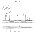
- FIG. 1 is a perspective view of a solar cell according to an example embodiment of the invention.
- FIG. 2 is a cross-sectional view taken along a line II-II of FIG. 1 ;
- FIG. 3 is a schematic view showing a solar cell module according to an example embodiment of the present invention.
- FIG. 1 is a perspective view of a solar cell according to an example embodiment of the invention and FIG. 2 is a cross-sectional view taken along a line II-II of FIG. 1 .
- a solar cell 1 includes a substrate 110, an emitter region 121 positioned in (at) a surface (hereinafter, referred to as 'a front surface') of the substrate 110 on which light is incident, an anti-reflection layer 130 on the emitter region 120, a front electrode unit 140 positioned on the front surface of the substrate 110 and connected to the emitter region 121, a rear electrode 151 positioned on a surface (a rear surface) of the substrate 110, opposite the front surface of the substrate 110, on which the light is not incident and connected to the substrate 110, and a back surface field (BSF) region 171 positioned between the substrate 110 and the rear electrode 151.
- BSF back surface field
- the substrate 110 is a semiconductor substrate, and may be formed of first conductive type silicon, for example, p-type silicon, though not required.
- the silicon is polycrystalline silicon, but the silicon may be single crystal silicon or others in other embodiments.
- a group III element impurity such as boron (B), gallium (Ga), and indium (In) may be doped in the substrate 110.
- the substrate 110 may be of an n-type.
- a group V element impurity such as phosphorus (P), arsenic (As), and antimony (Sb) may be doped in the substrate 110.
- the substrate 110 may be a material other than silicon.
- the emitter region 121 is an impurity region containing an impurity (e.g., an n-type impurity) of a second conductive type opposite the first conductive type of the substrate 110.
- the emitter region 121 is substantially positioned in (at) the entire front surface of the substrate 110, on which light is incident.
- the emitter region 121 has a sheet resistance of about 80 ⁇ /sq. to 150 ⁇ /sq.
- a deviation of the sheet resistance according to a position variation in the emitter region 121 of the embodiment is about ⁇ 15 ⁇ /sq., in a unit area of about 10 ⁇ m ⁇ 10 ⁇ m.
- the unit area for measuring the deviation of the sheet resistance may be varied.
- the emitter region 121 has a thickness of about 150nm to 450nm.
- the emitter region 121 has the sheet resistance of about 100 ⁇ /sq.
- the emitter region 121 that is, the front surface of the substrate 110, is textured to form a textured surface that is an uneven surface. Though somewhat exaggerated in FIGS. 1 and 2 for purposes of illustration, the textured surface includes a plurality of jagged portions as shown.
- the front surface of the substrate 110 is etched by a dry etching method such as a reaction ion etching (RIE) method to form the textured surface.
- RIE reaction ion etching
- Each of the jagged portions may have diameter (i.e., the maximum diameter) and the height of hundreds of nanometers, for example, that are equal to or less than 1 ⁇ m, such as about 300nm (0.3 ⁇ m) to 800nm (0.8 ⁇ m).
- each jagged portion Since a size of each jagged portion is small, such as hundreds of nanometers, and is of a sub-micron size, a refractive index from the apex of each jagged portion to the substrate 110 is changed, for example, gradually or abruptly. That is, an upper portion of the jagged portion has a refractive index similar to that of air, while a lower portion of the jagged portion has a refractive index similar to that of silicon (Si) contained in the substrate 110. Thus, in each jagged portion, a layer stack effect obtained by stacked layers with different refractive index being continuously changed is generated.
- reflectance for example, average weighted reflectance
- an anti-reflection efficiency of light increases to improve an efficiency of the solar cell 1.
- the sheet resistance of the emitter region 121 in this embodiment is greater than that of an emitter region according to a comparative example (or a convention example), and the thickness (the impurity doped depth) of the emitter region 121 in this embodiment is less than that of the emitter region of the comparative example.
- the emitter region according to the comparative example is formed on a textured surface that is formed on the surface of a substrate by a wet etching method and has a plurality of projections with a size (a diameter (d1) and/or a height (d2)) that is of micrometers.
- the emitter region of the comparative example has a sheet resistance of about 50 ⁇ /sq. to 70 ⁇ /sq., and a thickness of about 300nm to 500nm.
- the thickness of the emitter region 121 influences (or is influenced by) process conditions such as a process temperature and a process time, etc., given the same process temperate, and as the thickness of the emitter region 121 decreases, the time it takes for forming the emitter region 121 becomes shorter.
- the emitter region 121 forms a p-n junction with the substrate 110.
- the boundary portion that is, a p-n junction portion, between the substrate 110 and the emitter region 121 also has an uneven surface similar to the textured surface of the substrate 110.
- a plurality of electron-hole pairs which are generated by incident light on the semiconductor substrate 110, are separated into electrons and holes, respectively, and the separated electrons move toward the n-type semiconductor and the separated holes move toward the p-type semiconductor.
- the separated holes move toward the substrate 110 and the separated electrons move toward the emitter region 121.
- the emitter region 121 forms the p-n junction with the substrate 110, when the substrate 110 is of the n-type, then the emitter region 121 is of the p-type, in contrast to the embodiment discussed above, so that the separated electrons move toward the substrate 110 and the separated holes move toward the emitter region 121.
- the emitter region 121 when the emitter region 121 is of the n-type, the emitter region 121 may be formed by doping the substrate 110 with the group V element impurity such as P, As, Sb, etc., while when the emitter region 121 is of the p-type, the emitter region 121 may be formed by doping the substrate 110 with the group III element impurity such as B, Ga, In, etc.
- the anti-reflection layer 130 positioned on the emitter region 121 is preferably, but not necessarily, made of silicon nitride (SiNx) or silicon oxide (SiOx), etc.
- the anti-reflection layer 130 reduces reflectance of light incident on the substrate 110 and increases selectivity of a specific wavelength band, thereby increasing the efficiency of the solar cell 1.
- the anti-reflection layer 130 also performs a passivation function to change defects such as dangling bonds, mainly existing at the surface portion of the substrate 110, into stable bonds to reduce charge disappearance caused by the defects.
- the anti-reflection layer 130 is made of silicon nitride (SiNx)
- the anti-reflection layer (SiNx layer) 130 has an electric characteristic of a positive charge, and the anti-reflection layer 130 disturbs the hole movement toward the front surface of the substrate 110, but attracts the electrons toward the front surface of the substrate 110, to thereby improve the transmission efficiency of the charges (i.e., the electrons).
- the anti-reflection layer 130 has a single-layered structure, but the anti-reflection layer 130 may have a multi-layered structure such as a double-layered structure in other embodiments.
- the anti-reflection layer 130 may be omitted, if desired.
- the front electrode unit 140 includes a plurality of front electrodes 141 and a plurality of charge collectors (hereinafter, referred to as 'a plurality of front electrode charge collectors') for the front electrodes 142.
- the plurality of front electrodes 141 are physically and electrically connected to the emitter region 121 and are spaced apart from each other by a predetermined distance to be parallel to each other.
- the front electrodes 141 collect charges, for example, electrons, moving toward the emitter region 121.
- an aspect ratio (a ratio of thickness to width) of each front electrode 141 is about 1 to 1.5.
- each of the front electrodes 141 may have a width (w1) of about 0.02mm(20 ⁇ m) to 0.08mm(80 ⁇ m) and have a thickness (or height) of about 0.03mm(30 ⁇ m) to 0.08mm(80 ⁇ m).
- the thickness of the front electrode 141 is measured at an approximately middle portion of the front electrode 141 that is between two adjacent front electrode charge collectors 142.
- a distance (D) between two adjacent front electrodes 141 may be approximately 1.6mm(160 ⁇ m) to 2.0mm(200 ⁇ m).
- a distance of two adjacent front electrodes according to the comparative example is about 2.1 to 2.3mm.
- each front electrode 141 is less than that of each front electrode of the comparative example, but the thickness of each front electrode 141 is more than that of each front electrode of the comparative example.
- each front electrode according to the comparative example has a width of about 0.08mm to 0.12mm and a thickness of about 0.015mm to 0.025mm.
- the size of each projection of the textured surface is of micrometers dimensions, and thereby the emitter region at the substrate is formed along in the shape of the textured surface. Further, by characteristics of a process for forming the emitter region, the thicknesses of portions of the emitter region which are formed at an apex portion of each projection of the textured surface, are greater than those of portions of the emitter region which are formed at a side portion or a lower portion of (or between) each projection (i.e. a valley portion) of the textured surface. Thereby, in the comparative example, the p-n junction portion is an uneven surface having unevenness that is about equal to the textured surface.
- each jagged portion formed at the textured surface has the size of hundreds of nanometers (or has nanometer dimensions).
- the emitter region 121 is formed to have a thickness of about 300nm to 500nm similar to the emitter region of the comparative example, the emitter region 121 of the embodiment is formed into an internal portion of the substrate 110, at which the plurality of jagged portions are not formed, as well as at a portion with an uneven portion (the textured surface). That is, the emitter region will have a thickness of 300nm to 500nm from the textured surface, and the p-n junction portion S1 is close to being an almost flat surface.
- the jagged portions of the embodiment is of a smaller size than that of the comparative example, the doping of the impurity (e.g., an n-type impurity) of a second conductive type into the substrate 110 is less affected by the presence of the jagged portions, and the emitter layer 121 is formed to have a substantially smooth p-n junction with substrate 110.
- the impurity e.g., an n-type impurity
- the textured surface is formed by use of the dry etching method as in the embodiment, but if the emitter region is formed to have the thickness of the comparative example, then a distance between the p-n junction portion (located in the depths of the substrate 110) and the surface of the substrate 110 is far larger than that of the comparative example, and the area of the emitter region also further increases as compared to the comparative example.
- an amount of light of a short wavelength range which does not reach the p-n junction portion increases, and thereby there is a problem of reduced current amount generated by the light of the short wavelength range.
- the thickness of the emitter region 121 is reduced in this embodiment, the current loss by light of the short wavelength range not reaching the p-n junction is reduced or prevented.
- the sheet resistance of the emitter region 121 increases due to the thickness reduction of the emitter region 121, and the surface area of the textured surface is also increased by the size of the jagged portions having dimensions of hundreds of nanometers. Thereby, the movement distance of charges mainly moving along the surface of the substrate 110 and the sheet resistance may increase, and thereby the charge disappearance may be occurring.
- the distance between two adjacent front electrodes 141 is shortened in comparison to the comparative example.
- the movement distance of the charges moving to adjacent front electrodes 141 is reduce to decrease or prevent the charge disappearance.
- the number of front electrodes 141 is increased by the shortened distance between two adjacent front electrodes 141, and thereby the incident area of light is reduced.
- the width of each front electrode 141 is also reduced, the incident area of light is not so reduced to prevent the loss of light incident on the substrate 110.
- the thickness of each front electrode 141 is increased, the increase of contact resistance between the emitter region 121 and the front electrodes 141 is prevented or reduced.
- the plurality of first electrodes 141 are formed over the plurality of jagged portions so that a number of the plurality of jagged portions are disposed within a cross sectional width direction of the plurality of first electrodes 141.
- the number of such jagged portions is at least 10. Similar or greater number of jagged portions is disposed within a cross sectional width direction of the plurality of first electrode charge collectors 142.
- the sheet resistance of the emitter region 121 is increased by the size decrement of each jagged portion so as to have high sheet resistance characteristics, the charge disappearance by the incremented sheet resistance of the emitter region 121 and the enlarged surface area of the substrate 110 are prevented or reduced, and the decrement of the incident area of light and the decrement of the charges amount transmitted from the emitter region 121 and the front electrodes 141 are also prevented or reduced.
- each front electrode 141 When the width and thickness of each front electrode 141 is lower than a lower limit, the front electrodes 141 do not normally function, and when the width and thickness of each front electrode 141 exceed an upper limit, the width of each front electrode 141 are unnecessarily increased to reduce the incident area of light and waste the material of the front electrodes 141 thereby. In particular, when the thickness of each front electrode 141 exceeds the upper limit, the formation of the front electrodes 141 becomes difficult.
- the plurality of front electrode charge collectors 142 extend in a direction crossing the front electrodes 141 and are electrically and physically connected to the plurality of front electrodes 141 as well as the emitter region 121.
- the plurality of front electrode charge collectors 142 are positioned on the same level layer as the front electrodes 141 and are electrically and physically connected to the plurality of front electrodes 141 at positions crossing each front electrode 141.
- each of the plurality of front electrodes 141 has a stripe shape extending in a horizontal or vertical direction and each of the plurality of front electrode charge collectors 142 has a stripe shape extending in a vertical or horizontal direction, and thereby the front electrode unit 140 is positioned to have a matrix structure at the front surface of the substrate 110.
- the front electrode charge collectors 142 collect the charges, for example, electrons, transferred from the front electrodes 141.
- the front electrode charge collectors 142 are connected to an external device by a conductive tape, etc., and thereby output the collected charges to the external device through the conductive tape, etc.
- each front electrode charge collector 142 collects and transfers the charges collected by the connected front electrodes 141 thereto, a width (w2) of each front electrode charge collector 142 is more than the width (w1) of each front electrode 141.
- the width of the front electrode charge collector 142 and the distance between two adjacent front electrode charge collectors 142 may be changed based on the number of front electrode charge collectors 142.
- each front electrode charge collector 142 when the number of the front electrode charge collectors 142 is two, the width of each front electrode charge collector 142 may be about 1.9mm to 2.2mm and the distance between two adjacent front electrode charge collectors 142 may be about 50mm to 55mm. When the number of the front electrode charge collectors 142 is three, the width of each front electrode charge collector 142 may be about 1.3mm to 1.7mm and the distance between two adjacent front electrode charge collectors 142 may be about 25mm to 30mm.
- each front electrode 141 when the width of each front electrode 141 is about 0.02mm, the width of each front electrode charge collector 142 may be about 1.3mm to 2.2mm, and when the width of each front electrode 141 is about 0.08mm, the width of each front electrode charge collector 142 may be about 1.3mm to 2.2mm.
- a ratio of the width of the front electrode 141 to the width of the front electrode charge collector 142 may be 1 : about 16.25 to 110.
- each front electrode charge collector 142 is equal to or greater than that of each front electrode 141.
- each front electrode charge collector 142 may be about 0.035mm (35 ⁇ m) to 1.0mm (100 ⁇ m). More specifically, when the thickness of the front electrode is about 0.03mm, the thickness of the front electrode charge collector 142 may be 0.035mm to 1.0mm, and when the thickness of the front electrode is about 0.08mm, the thickness of the front electrode charge collector 142 may be about 0.08mm to 1.0mm. Thereby, a ratio of the thickness of the front electrode 141 to the thickness of the front electrode charge collector 142 may be 1: about 1 to 3.3.
- a thickness difference between the front electrode 141 and the front electrode charge collector 142 is generated because the width of the front electrode charge collector 142 is larger than that of the front electrode 141.
- a paste containing Ag and Pb, etc. is printed on the anti-reflection layer 130 of the substrate 110 using a screen printing method to form a paste pastern for the front electrode unit 140, and then the substrate 110 with the printed paste pattern is heated at a predetermined temperature in a thermal process.
- portions of the anti-reflection layer 130 are etched by a Pb component contained in the paste pattern, and thereby the paste pattern comes in contact with the emitter region 121 to form the front electrode unit 140 contacting the emitter region 121.
- the plurality of jagged portions are disposed within the cross sectional width direction of the plurality of first electrode charge collectors 142 and/or a cross sectional width direction of the plurality of first electrodes.
- the width of the front electrode 141 is far less than that of the front electrode charge collector 142, during processes for forming the front electrode unit 140 such as the thermal process, a thickness reduction amount of a portion of the paste pattern for the front electrodes 141 is larger than that of a portion of the paste pattern for the front electrode charge collectors 142. Thereby, the thickness of the front electrode 141 is equal to or less than that of the front electrode charge collector 142.
- the paste for forming the front electrode unit 140 need not contain Pb.
- the front electrode unit 140 is formed using a paste containing an environment-friendly material that will perform the function of Pb instead, or by using other means for forming the paste pattern. Thus, environment pollution is prevented or reduced.
- the front electrode unit 140 When the front electrode unit 140 is formed using the paste containing Pb, the front electrode unit 140 then includes Pb, while when the front electrode unit 140 is formed using the paste not containing Pb, then Pb is not detected in the front electrode unit 140.
- the front electrode unit 140 including the plurality of front electrode 141 and the plurality of front electrode charge collectors 142 may be made of at least one conductive material selected from the group consisting of nickel (Ni), copper (Cu), aluminum (Al), tin (Sn), zinc (Zn), indium (In), titanium (Ti), gold (Au), and a combination thereof.
- Other conductive metal materials may be used.
- front electrodes 141 and front electrode charge collectors 142 are only an example, and thereby may be changed.
- the anti-reflection layer 130 is mainly positioned on portions of the first emitter region 121, on which the front electrode unit 140 is not positioned.
- the front electrode unit 140 is formed to have a thickness and/or width.
- the rear electrode 151 is substantially positioned on the entire rear surface of the substrate 110.
- the rear electrode 151 contains a conductive material such as aluminum (Al) and is connected to the substrate 110.
- the rear electrode 151 collects charges, for example, holes, moving toward the substrate 110 and output the charges to the external device.
- the rear electrode 151 may be made of a conductive material of at least one selected from the group consisting of Ni, Cu, Ag, Sn, Zn, In, Ti, Au, and a combination thereof. Other conductive materials may be used.
- the back surface field region 171 positioned between the rear electrode 151 and the substrate 110 is an area heavily doped by an impurity of the same conductive type as the substrate 110, and thereby, in this embodiment, the back surface field region 171 may be a p + -type area having an impurity doped concentration heavier than that of the substrate 110.
- a potential barrier is formed by an impurity doped concentration difference between the substrate 110 and the back surface field region 171, thereby disturbing the movement of charges (for example, electrons) to a rear portion of the substrate 110. Accordingly, the back surface field region 171 prevents or reduces the recombination and/or the disappearance of the separated electrons and holes at the rear surface of the substrate 110.
- the solar cell 1 may further include a plurality of charge collectors (a plurality of rear electrode charge collectors) for the rear electrode 151 positioned on the rear surface of the substrate 110.
- the plurality of rear electrode charge collectors are electrically connected to the substrate 110 to collect the charges transferred from the rear electrode 151 and output the charges to the external device.
- the plurality of rear electrode charge collectors are positioned to correspond to the front electrode charge collectors 142 of the front electrode unit 140.
- the plurality of rear electrode charge collectors may be made of a material with conductivity greater than that of the front electrode 151.
- the plurality of rear electrode charge collectors contain at least one conductive material such Ag.
- a paste for forming the rear electrode 151 and the rear electrode charge collectors contains Al and/or Ag, but does not contain Pb.
- the electron-hole pairs are separated by the p-n junction of the substrate 110 and the emitter region 121, and the separated electrons move toward the emitter region 121 of the n-type and the separated holes move toward the substrate 110 of the p-type.
- the electrons that move toward the emitter region 121 are mainly collected by the front electrodes 141 and moves along the front electrode charge collectors 142, while the holes that move toward the substrate 110 are collected by the rear electrode 151.
- the front electrode charge collectors 142 and the rear electrode 151 are connected to electric wires, current flows therein to thereby enable use of the current for electric power.
- the widths of the front electrodes 141 are reduced, the light incident area of the solar cell 1 increases to improve an efficiency of the solar cell 1.
- the wire resistance of the front electrodes 141 does not increase due to the offsetting thickness increment of the front electrodes 141.
- the plurality of solar cells 1 may be electrically connected in series or in parallel for more efficient use to form a solar cell module.
- FIG. 3 is a schematic view showing a solar cell module according to an example embodiment of the present invention.
- the solar cell module 100 includes a plurality of solar cells 1, protection films 20a and 20b for protecting the solar cells 1, a transparent member 40 positioned on the protection film 20a (hereinafter, 'an upper protection film') positioned on the light receiving surface of the solar cell 1, and a back sheet 50 disposed under the protection film 20b (hereinafter, 'a lower protection film') positioned on the opposite side of the light receiving surface on which light is not incident.
- the back sheet 50 prevents moisture from permeating to the back surface of the solar cell module 100 and hence protects the solar cells 1 from an outside environment.
- the back sheet 50 of this type may have a multilayered structure, such as a layer for preventing permeation of moisture and oxygen, a layer for preventing chemical corrosion, and a layer having insulation characteristics. etc.
- the upper and lower protection films 20a and 20b prevent the corrosion of metals caused by moisture permeation and protect the solar cell module 100 from an impact.
- the upper and lower protection films 20a and 20b of this type are integrated with the solar cells 1 during a lamination process, and are disposed on the upper and lower portions of the solar cells 1.
- These protection films 20a and 20b may be made of ethylene vinyl acetate (EVA) and the like.
- the transparent member 40 positioned on the upper protection film 20a is made of tempered glass having high transmittance and excellent damage prevention function.
- the tempered glass may be a low iron tempered glass having a low iron content.
- the inner surface of the transparent member 40 may be embossed in order to increase light scattering effect. Other materials for the transparent member 40 may be used.
- the solar cells 1 are arranged in a matrix structure.
- the solar cells 1 has a 4x4 matrix structure, but the embodiment is not limited thereto and the number of solar cells 1 disposed in respective row and column directions may be adjusted if required.
- the solar cells 1 are electrically connected in series to neighboring solar cells 1 by a plurality of connectors 70.
- the plurality of connectors 70 contain a conductive material and is a ribbon shape.
- the solar cell module 100 is manufactured by a method sequentially including testing the plurality of solar cells 1, electrically connecting the tested solar cells 1 to one another using the connectors 70, successively disposing the back sheet 50, the lower passivation layer 20b, the solar cells 1, the upper passivation layer 20a, and the transparent member 40 from the bottom of the solar cell module 100 in the order named, performing the lamination process in a vacuum state to form an integral body of the components 1, 20a, 20b, 40, and 50, performing an edge trimming process, testing the completed solar cell module 100, and the like.
- the solar cell module 100 integrated as one product by the laminating process is housed by a frame and thereby protected from the outside environment or an impact.
- the frame may be made of a material preventing the corrosion or deformation due to the outside environment, such as aluminum coated by an insulating material, and may have a structure by which drainage, installation and construction are easily performed.
- the solar cell module 100 further includes a junction box positioned under back sheet 50.
- the junction box finally collects current and voltage generated in the solar cells 1.
Landscapes
- Photovoltaic Devices (AREA)
Applications Claiming Priority (1)
| Application Number | Priority Date | Filing Date | Title |
|---|---|---|---|
| KR1020100044568A KR101579320B1 (ko) | 2010-05-12 | 2010-05-12 | 태양 전지 |
Publications (3)
| Publication Number | Publication Date |
|---|---|
| EP2395553A2 true EP2395553A2 (de) | 2011-12-14 |
| EP2395553A3 EP2395553A3 (de) | 2016-06-22 |
| EP2395553B1 EP2395553B1 (de) | 2018-10-10 |
Family
ID=44141556
Family Applications (1)
| Application Number | Title | Priority Date | Filing Date |
|---|---|---|---|
| EP10015635.5A Active EP2395553B1 (de) | 2010-05-12 | 2010-12-14 | Solarzelle |
Country Status (4)
| Country | Link |
|---|---|
| US (1) | US10566472B2 (de) |
| EP (1) | EP2395553B1 (de) |
| KR (1) | KR101579320B1 (de) |
| CN (1) | CN102244116B (de) |
Families Citing this family (10)
| Publication number | Priority date | Publication date | Assignee | Title |
|---|---|---|---|---|
| KR20120140026A (ko) * | 2011-06-20 | 2012-12-28 | 엘지전자 주식회사 | 태양전지 |
| CN103165689B (zh) * | 2011-12-12 | 2015-10-28 | 茂迪股份有限公司 | 太阳能电池及其制造方法 |
| KR101860919B1 (ko) * | 2011-12-16 | 2018-06-29 | 엘지전자 주식회사 | 태양 전지 및 이의 제조 방법 |
| KR101838278B1 (ko) * | 2011-12-23 | 2018-03-13 | 엘지전자 주식회사 | 태양 전지 |
| CN102522505B (zh) * | 2012-01-14 | 2014-08-20 | 西安电子科技大学 | 无机与有机混合太阳能电池 |
| KR20130096822A (ko) * | 2012-02-23 | 2013-09-02 | 엘지전자 주식회사 | 태양 전지 및 그 제조 방법 |
| KR101921738B1 (ko) * | 2012-06-26 | 2018-11-23 | 엘지전자 주식회사 | 태양 전지 |
| US9105775B2 (en) * | 2012-06-28 | 2015-08-11 | International Business Machines Corporation | Textured multi-junction solar cell and fabrication method |
| TWI496302B (zh) * | 2013-01-31 | 2015-08-11 | Motech Ind Inc | 太陽能電池 |
| US9876045B2 (en) * | 2015-05-06 | 2018-01-23 | Cista System Corp. | Back side illuminated CMOS image sensor arrays |
Family Cites Families (12)
| Publication number | Priority date | Publication date | Assignee | Title |
|---|---|---|---|---|
| US4590327A (en) * | 1984-09-24 | 1986-05-20 | Energy Conversion Devices, Inc. | Photovoltaic device and method |
| ES2068304T3 (es) | 1990-09-28 | 1995-04-16 | Siemens Solar Gmbh | Mordentado estructural quimico-humedo de silicio. |
| JP2992464B2 (ja) | 1994-11-04 | 1999-12-20 | キヤノン株式会社 | 集電電極用被覆ワイヤ、該集電電極用被覆ワイヤを用いた光起電力素子及びその製造方法 |
| JP2002164555A (ja) | 2000-11-27 | 2002-06-07 | Kyocera Corp | 太陽電池およびその形成方法 |
| US20030178057A1 (en) * | 2001-10-24 | 2003-09-25 | Shuichi Fujii | Solar cell, manufacturing method thereof and electrode material |
| WO2005109524A1 (ja) * | 2004-05-07 | 2005-11-17 | Mitsubishi Denki Kabushiki Kaisha | 太陽電池及びその製造方法 |
| CN101840962A (zh) * | 2005-11-08 | 2010-09-22 | Lg电子株式会社 | 高效太阳能电池及其制备方法 |
| JP4429306B2 (ja) | 2006-12-25 | 2010-03-10 | 三洋電機株式会社 | 太陽電池セル及び太陽電池モジュール |
| KR20100032900A (ko) | 2007-07-18 | 2010-03-26 | 아이엠이씨 | 에미터 구조체를 제조하는 방법 및 그로부터 생성되는 에미터 구조체들 |
| JP5094509B2 (ja) * | 2008-03-31 | 2012-12-12 | 三洋電機株式会社 | 太陽電池モジュール |
| KR20090118333A (ko) * | 2008-05-13 | 2009-11-18 | 삼성전자주식회사 | 태양전지 및 그 형성방법 |
| KR100990109B1 (ko) * | 2008-07-28 | 2010-10-29 | 엘지전자 주식회사 | 태양전지 및 그의 제조방법 |
-
2010
- 2010-05-12 KR KR1020100044568A patent/KR101579320B1/ko active Active
- 2010-12-09 US US12/964,384 patent/US10566472B2/en active Active
- 2010-12-14 EP EP10015635.5A patent/EP2395553B1/de active Active
-
2011
- 2011-01-28 CN CN201110032238.9A patent/CN102244116B/zh active Active
Non-Patent Citations (1)
| Title |
|---|
| None |
Also Published As
| Publication number | Publication date |
|---|---|
| CN102244116A (zh) | 2011-11-16 |
| EP2395553A3 (de) | 2016-06-22 |
| KR101579320B1 (ko) | 2015-12-21 |
| US10566472B2 (en) | 2020-02-18 |
| EP2395553B1 (de) | 2018-10-10 |
| CN102244116B (zh) | 2014-04-09 |
| KR20110125041A (ko) | 2011-11-18 |
| US20110139239A1 (en) | 2011-06-16 |
Similar Documents
| Publication | Publication Date | Title |
|---|---|---|
| EP2395553B1 (de) | Solarzelle | |
| USRE47484E1 (en) | Solar cell | |
| EP2380211B1 (de) | Solarzellenmodul mit anschlussstück und herstellungsverfahren dafür | |
| US20190245101A1 (en) | Solar cell | |
| EP3457443B1 (de) | Solarzelle und solarzellenmodul | |
| KR101295552B1 (ko) | 태양 전지 및 그 제조 방법 | |
| US20110132426A1 (en) | Solar cell module | |
| US8884158B2 (en) | Solar cell and solar cell module | |
| EP2341548B1 (de) | Solarzellenmodul | |
| US20110197964A1 (en) | Solar cell | |
| US20140332060A1 (en) | Solar cell and solar cell module | |
| EP2458649B1 (de) | Solarzelle | |
| KR101733055B1 (ko) | 태양 전지 모듈 | |
| JP2013175706A (ja) | 太陽電池及びその製造方法 | |
| CN103515456A (zh) | 太阳能电池 | |
| KR101621980B1 (ko) | 태양 전지 및 그 제조 방법 | |
| KR101714779B1 (ko) | 태양전지 및 이의 제조 방법 | |
| US20110132425A1 (en) | Solar cell module | |
| KR101579321B1 (ko) | 태양 전지의 제조 방법 | |
| KR20130080662A (ko) | 태양전지 모듈 | |
| KR20170090781A (ko) | 태양 전지 및 이의 제조 방법 | |
| KR20130049898A (ko) | 태양전지 모듈 및 이를 구비한 태양광 발전 시스템 |
Legal Events
| Date | Code | Title | Description |
|---|---|---|---|
| 17P | Request for examination filed |
Effective date: 20101214 |
|
| AK | Designated contracting states |
Kind code of ref document: A2 Designated state(s): AL AT BE BG CH CY CZ DE DK EE ES FI FR GB GR HR HU IE IS IT LI LT LU LV MC MK MT NL NO PL PT RO RS SE SI SK SM TR |
|
| AX | Request for extension of the european patent |
Extension state: BA ME |
|
| PUAI | Public reference made under article 153(3) epc to a published international application that has entered the european phase |
Free format text: ORIGINAL CODE: 0009012 |
|
| PUAL | Search report despatched |
Free format text: ORIGINAL CODE: 0009013 |
|
| AK | Designated contracting states |
Kind code of ref document: A3 Designated state(s): AL AT BE BG CH CY CZ DE DK EE ES FI FR GB GR HR HU IE IS IT LI LT LU LV MC MK MT NL NO PL PT RO RS SE SI SK SM TR |
|
| AX | Request for extension of the european patent |
Extension state: BA ME |
|
| RIC1 | Information provided on ipc code assigned before grant |
Ipc: H01L 31/0236 20060101ALI20160519BHEP Ipc: H01L 31/0224 20060101AFI20160519BHEP Ipc: H01L 31/068 20120101ALI20160519BHEP |
|
| GRAP | Despatch of communication of intention to grant a patent |
Free format text: ORIGINAL CODE: EPIDOSNIGR1 |
|
| STAA | Information on the status of an ep patent application or granted ep patent |
Free format text: STATUS: GRANT OF PATENT IS INTENDED |
|
| RIC1 | Information provided on ipc code assigned before grant |
Ipc: H01L 31/0224 20060101AFI20180417BHEP Ipc: H01L 31/0236 20060101ALI20180417BHEP Ipc: H01L 31/068 20060101ALI20180417BHEP |
|
| INTG | Intention to grant announced |
Effective date: 20180517 |
|
| RIN1 | Information on inventor provided before grant (corrected) |
Inventor name: HA, MANHYO Inventor name: JANG, DAEHEE Inventor name: KIM, JONGHWAN Inventor name: LEE, GIWON Inventor name: KANG, JUWAN Inventor name: LEE, KYOUNGSOO |
|
| GRAS | Grant fee paid |
Free format text: ORIGINAL CODE: EPIDOSNIGR3 |
|
| GRAA | (expected) grant |
Free format text: ORIGINAL CODE: 0009210 |
|
| STAA | Information on the status of an ep patent application or granted ep patent |
Free format text: STATUS: THE PATENT HAS BEEN GRANTED |
|
| AK | Designated contracting states |
Kind code of ref document: B1 Designated state(s): AL AT BE BG CH CY CZ DE DK EE ES FI FR GB GR HR HU IE IS IT LI LT LU LV MC MK MT NL NO PL PT RO RS SE SI SK SM TR |
|
| REG | Reference to a national code |
Ref country code: GB Ref legal event code: FG4D |
|
| REG | Reference to a national code |
Ref country code: CH Ref legal event code: EP Ref country code: AT Ref legal event code: REF Ref document number: 1052244 Country of ref document: AT Kind code of ref document: T Effective date: 20181015 |
|
| REG | Reference to a national code |
Ref country code: IE Ref legal event code: FG4D Ref country code: DE Ref legal event code: R096 Ref document number: 602010054160 Country of ref document: DE |
|
| REG | Reference to a national code |
Ref country code: NL Ref legal event code: MP Effective date: 20181010 |
|
| REG | Reference to a national code |
Ref country code: LT Ref legal event code: MG4D |
|
| REG | Reference to a national code |
Ref country code: AT Ref legal event code: MK05 Ref document number: 1052244 Country of ref document: AT Kind code of ref document: T Effective date: 20181010 |
|
| PG25 | Lapsed in a contracting state [announced via postgrant information from national office to epo] |
Ref country code: NL Free format text: LAPSE BECAUSE OF FAILURE TO SUBMIT A TRANSLATION OF THE DESCRIPTION OR TO PAY THE FEE WITHIN THE PRESCRIBED TIME-LIMIT Effective date: 20181010 |
|
| PG25 | Lapsed in a contracting state [announced via postgrant information from national office to epo] |
Ref country code: LV Free format text: LAPSE BECAUSE OF FAILURE TO SUBMIT A TRANSLATION OF THE DESCRIPTION OR TO PAY THE FEE WITHIN THE PRESCRIBED TIME-LIMIT Effective date: 20181010 Ref country code: HR Free format text: LAPSE BECAUSE OF FAILURE TO SUBMIT A TRANSLATION OF THE DESCRIPTION OR TO PAY THE FEE WITHIN THE PRESCRIBED TIME-LIMIT Effective date: 20181010 Ref country code: PL Free format text: LAPSE BECAUSE OF FAILURE TO SUBMIT A TRANSLATION OF THE DESCRIPTION OR TO PAY THE FEE WITHIN THE PRESCRIBED TIME-LIMIT Effective date: 20181010 Ref country code: LT Free format text: LAPSE BECAUSE OF FAILURE TO SUBMIT A TRANSLATION OF THE DESCRIPTION OR TO PAY THE FEE WITHIN THE PRESCRIBED TIME-LIMIT Effective date: 20181010 Ref country code: ES Free format text: LAPSE BECAUSE OF FAILURE TO SUBMIT A TRANSLATION OF THE DESCRIPTION OR TO PAY THE FEE WITHIN THE PRESCRIBED TIME-LIMIT Effective date: 20181010 Ref country code: BG Free format text: LAPSE BECAUSE OF FAILURE TO SUBMIT A TRANSLATION OF THE DESCRIPTION OR TO PAY THE FEE WITHIN THE PRESCRIBED TIME-LIMIT Effective date: 20190110 Ref country code: IS Free format text: LAPSE BECAUSE OF FAILURE TO SUBMIT A TRANSLATION OF THE DESCRIPTION OR TO PAY THE FEE WITHIN THE PRESCRIBED TIME-LIMIT Effective date: 20190210 Ref country code: NO Free format text: LAPSE BECAUSE OF FAILURE TO SUBMIT A TRANSLATION OF THE DESCRIPTION OR TO PAY THE FEE WITHIN THE PRESCRIBED TIME-LIMIT Effective date: 20190110 Ref country code: AT Free format text: LAPSE BECAUSE OF FAILURE TO SUBMIT A TRANSLATION OF THE DESCRIPTION OR TO PAY THE FEE WITHIN THE PRESCRIBED TIME-LIMIT Effective date: 20181010 Ref country code: FI Free format text: LAPSE BECAUSE OF FAILURE TO SUBMIT A TRANSLATION OF THE DESCRIPTION OR TO PAY THE FEE WITHIN THE PRESCRIBED TIME-LIMIT Effective date: 20181010 |
|
| PG25 | Lapsed in a contracting state [announced via postgrant information from national office to epo] |
Ref country code: SE Free format text: LAPSE BECAUSE OF FAILURE TO SUBMIT A TRANSLATION OF THE DESCRIPTION OR TO PAY THE FEE WITHIN THE PRESCRIBED TIME-LIMIT Effective date: 20181010 Ref country code: GR Free format text: LAPSE BECAUSE OF FAILURE TO SUBMIT A TRANSLATION OF THE DESCRIPTION OR TO PAY THE FEE WITHIN THE PRESCRIBED TIME-LIMIT Effective date: 20190111 Ref country code: AL Free format text: LAPSE BECAUSE OF FAILURE TO SUBMIT A TRANSLATION OF THE DESCRIPTION OR TO PAY THE FEE WITHIN THE PRESCRIBED TIME-LIMIT Effective date: 20181010 Ref country code: RS Free format text: LAPSE BECAUSE OF FAILURE TO SUBMIT A TRANSLATION OF THE DESCRIPTION OR TO PAY THE FEE WITHIN THE PRESCRIBED TIME-LIMIT Effective date: 20181010 Ref country code: PT Free format text: LAPSE BECAUSE OF FAILURE TO SUBMIT A TRANSLATION OF THE DESCRIPTION OR TO PAY THE FEE WITHIN THE PRESCRIBED TIME-LIMIT Effective date: 20190210 |
|
| REG | Reference to a national code |
Ref country code: DE Ref legal event code: R097 Ref document number: 602010054160 Country of ref document: DE |
|
| PG25 | Lapsed in a contracting state [announced via postgrant information from national office to epo] |
Ref country code: DK Free format text: LAPSE BECAUSE OF FAILURE TO SUBMIT A TRANSLATION OF THE DESCRIPTION OR TO PAY THE FEE WITHIN THE PRESCRIBED TIME-LIMIT Effective date: 20181010 Ref country code: IT Free format text: LAPSE BECAUSE OF FAILURE TO SUBMIT A TRANSLATION OF THE DESCRIPTION OR TO PAY THE FEE WITHIN THE PRESCRIBED TIME-LIMIT Effective date: 20181010 Ref country code: CZ Free format text: LAPSE BECAUSE OF FAILURE TO SUBMIT A TRANSLATION OF THE DESCRIPTION OR TO PAY THE FEE WITHIN THE PRESCRIBED TIME-LIMIT Effective date: 20181010 |
|
| REG | Reference to a national code |
Ref country code: CH Ref legal event code: PL |
|
| PLBE | No opposition filed within time limit |
Free format text: ORIGINAL CODE: 0009261 |
|
| STAA | Information on the status of an ep patent application or granted ep patent |
Free format text: STATUS: NO OPPOSITION FILED WITHIN TIME LIMIT |
|
| PG25 | Lapsed in a contracting state [announced via postgrant information from national office to epo] |
Ref country code: SK Free format text: LAPSE BECAUSE OF FAILURE TO SUBMIT A TRANSLATION OF THE DESCRIPTION OR TO PAY THE FEE WITHIN THE PRESCRIBED TIME-LIMIT Effective date: 20181010 Ref country code: LU Free format text: LAPSE BECAUSE OF NON-PAYMENT OF DUE FEES Effective date: 20181214 Ref country code: RO Free format text: LAPSE BECAUSE OF FAILURE TO SUBMIT A TRANSLATION OF THE DESCRIPTION OR TO PAY THE FEE WITHIN THE PRESCRIBED TIME-LIMIT Effective date: 20181010 Ref country code: MC Free format text: LAPSE BECAUSE OF FAILURE TO SUBMIT A TRANSLATION OF THE DESCRIPTION OR TO PAY THE FEE WITHIN THE PRESCRIBED TIME-LIMIT Effective date: 20181010 Ref country code: SM Free format text: LAPSE BECAUSE OF FAILURE TO SUBMIT A TRANSLATION OF THE DESCRIPTION OR TO PAY THE FEE WITHIN THE PRESCRIBED TIME-LIMIT Effective date: 20181010 Ref country code: EE Free format text: LAPSE BECAUSE OF FAILURE TO SUBMIT A TRANSLATION OF THE DESCRIPTION OR TO PAY THE FEE WITHIN THE PRESCRIBED TIME-LIMIT Effective date: 20181010 |
|
| 26N | No opposition filed |
Effective date: 20190711 |
|
| REG | Reference to a national code |
Ref country code: IE Ref legal event code: MM4A |
|
| GBPC | Gb: european patent ceased through non-payment of renewal fee |
Effective date: 20190110 |
|
| REG | Reference to a national code |
Ref country code: BE Ref legal event code: MM Effective date: 20181231 |
|
| PG25 | Lapsed in a contracting state [announced via postgrant information from national office to epo] |
Ref country code: SI Free format text: LAPSE BECAUSE OF FAILURE TO SUBMIT A TRANSLATION OF THE DESCRIPTION OR TO PAY THE FEE WITHIN THE PRESCRIBED TIME-LIMIT Effective date: 20181010 Ref country code: FR Free format text: LAPSE BECAUSE OF NON-PAYMENT OF DUE FEES Effective date: 20181231 Ref country code: IE Free format text: LAPSE BECAUSE OF NON-PAYMENT OF DUE FEES Effective date: 20181214 |
|
| PG25 | Lapsed in a contracting state [announced via postgrant information from national office to epo] |
Ref country code: BE Free format text: LAPSE BECAUSE OF NON-PAYMENT OF DUE FEES Effective date: 20181231 |
|
| PG25 | Lapsed in a contracting state [announced via postgrant information from national office to epo] |
Ref country code: CH Free format text: LAPSE BECAUSE OF NON-PAYMENT OF DUE FEES Effective date: 20181231 Ref country code: GB Free format text: LAPSE BECAUSE OF NON-PAYMENT OF DUE FEES Effective date: 20190110 Ref country code: LI Free format text: LAPSE BECAUSE OF NON-PAYMENT OF DUE FEES Effective date: 20181231 |
|
| PG25 | Lapsed in a contracting state [announced via postgrant information from national office to epo] |
Ref country code: MT Free format text: LAPSE BECAUSE OF NON-PAYMENT OF DUE FEES Effective date: 20181214 |
|
| PG25 | Lapsed in a contracting state [announced via postgrant information from national office to epo] |
Ref country code: TR Free format text: LAPSE BECAUSE OF FAILURE TO SUBMIT A TRANSLATION OF THE DESCRIPTION OR TO PAY THE FEE WITHIN THE PRESCRIBED TIME-LIMIT Effective date: 20181010 |
|
| PG25 | Lapsed in a contracting state [announced via postgrant information from national office to epo] |
Ref country code: MK Free format text: LAPSE BECAUSE OF NON-PAYMENT OF DUE FEES Effective date: 20181010 Ref country code: HU Free format text: LAPSE BECAUSE OF FAILURE TO SUBMIT A TRANSLATION OF THE DESCRIPTION OR TO PAY THE FEE WITHIN THE PRESCRIBED TIME-LIMIT; INVALID AB INITIO Effective date: 20101214 Ref country code: CY Free format text: LAPSE BECAUSE OF FAILURE TO SUBMIT A TRANSLATION OF THE DESCRIPTION OR TO PAY THE FEE WITHIN THE PRESCRIBED TIME-LIMIT Effective date: 20181010 |
|
| REG | Reference to a national code |
Ref country code: DE Ref legal event code: R081 Ref document number: 602010054160 Country of ref document: DE Owner name: SHANGRAO JINKO SOLAR TECHNOLOGY DEVELOPMENT CO, CN Free format text: FORMER OWNER: LG ELECTRONICS INC., SEOUL, KR Ref country code: DE Ref legal event code: R082 Ref document number: 602010054160 Country of ref document: DE Representative=s name: DREISS PATENTANWAELTE PARTG MBB, DE Ref country code: DE Ref legal event code: R081 Ref document number: 602010054160 Country of ref document: DE Owner name: SHANGRAO XINYUAN YUEDONG TECHNOLOGY DEVELOPMEN, CN Free format text: FORMER OWNER: LG ELECTRONICS INC., SEOUL, KR |
|
| REG | Reference to a national code |
Ref country code: DE Ref legal event code: R081 Ref document number: 602010054160 Country of ref document: DE Owner name: SHANGRAO XINYUAN YUEDONG TECHNOLOGY DEVELOPMEN, CN Free format text: FORMER OWNER: SHANGRAO JINKO SOLAR TECHNOLOGY DEVELOPMENT CO., LTD, SHANGRAO, JIANGXI PROVINCE, CN |
|
| REG | Reference to a national code |
Ref country code: DE Ref legal event code: R079 Ref document number: 602010054160 Country of ref document: DE Free format text: PREVIOUS MAIN CLASS: H01L0031022400 Ipc: H10F0077200000 |
|
| PGFP | Annual fee paid to national office [announced via postgrant information from national office to epo] |
Ref country code: DE Payment date: 20251211 Year of fee payment: 16 |