EP2391011B1 - A programmable logic device having complex logic blocks with improved logic cell functionality - Google Patents
A programmable logic device having complex logic blocks with improved logic cell functionality Download PDFInfo
- Publication number
- EP2391011B1 EP2391011B1 EP11174213.6A EP11174213A EP2391011B1 EP 2391011 B1 EP2391011 B1 EP 2391011B1 EP 11174213 A EP11174213 A EP 11174213A EP 2391011 B1 EP2391011 B1 EP 2391011B1
- Authority
- EP
- European Patent Office
- Prior art keywords
- logic
- look
- carry
- multiplexer
- output
- Prior art date
- Legal status (The legal status is an assumption and is not a legal conclusion. Google has not performed a legal analysis and makes no representation as to the accuracy of the status listed.)
- Active
Links
Images


Classifications
-
- H—ELECTRICITY
- H03—ELECTRONIC CIRCUITRY
- H03K—PULSE TECHNIQUE
- H03K19/00—Logic circuits, i.e. having at least two inputs acting on one output; Inverting circuits
- H03K19/02—Logic circuits, i.e. having at least two inputs acting on one output; Inverting circuits using specified components
- H03K19/173—Logic circuits, i.e. having at least two inputs acting on one output; Inverting circuits using specified components using elementary logic circuits as components
- H03K19/177—Logic circuits, i.e. having at least two inputs acting on one output; Inverting circuits using specified components using elementary logic circuits as components arranged in matrix form
- H03K19/17724—Structural details of logic blocks
- H03K19/17728—Reconfigurable logic blocks, e.g. lookup tables
Definitions
- the present invention generally relates to Complex Logic Block (CLB) based Programmable Logic Devices (PLDs), and more particularly, CLBs including a plurality of slices, each having one or more logic cells with improved logic, register, arithmetic, logic packing and timing functions and capabilities.
- CLB Complex Logic Block
- PLDs Programmable Logic Devices
- a Programmable Logic Device is a semiconductor integrated circuit that contains fixed logic circuitry that can be programmed to perform a host of logic functions.
- PLDs are becoming increasingly popular for a number of reasons. Due to the advances of chip manufacturing technology, application specific integrated circuits (ASICs) designs have become incredibly complex. This complexity not only adds to design costs, but also the duration of time needed to develop an application specific design. To compound this problem, product life cycles are shrinking rapidly. As a result, it is often not feasible for original equipment manufacturers (OEMs) to design and use ASICs. OEMs are therefore relying more and more on PLDs. The same advances in fabrication technology have also resulted in PLDs with improved density and speed performance.
- Sophisticated programming software enables complex logic functions to be rapidly developed for PLDs. Furthermore, logic designs generally can also be easily migrated from one generation of PLDs to the next, further reducing product development times. The closing of the price-performance gap with ASICs and reduced product development times makes the use of PLDs compelling for many OEMs.
- the architecture of most PLDs defines a two-dimensional array of logic blocks. Row and column inter-logic block lines, typically of varying length and speed, provide signal and clock interconnects between the blocks of logic in the array.
- the blocks of logic are referred to as Complex Logic Blocks or CLBs.
- CLBs Complex Logic Blocks
- Each CLB includes a pair of slices. The two slices in each CLB do not have direct connections with one another and are organized in different columns. The slices in each column, however, are connected to the slices of the above and below CLBs, creating independent carry chains. For example, the slices in the first and second columns each receive a carry in (Cin) signal from the previous CLB and generate a carry out signal provided to the next CLB respectively.
- Cin carry in
- Each slice typically includes four logic cells (hereafter simply referred to as "cells").
- Each cell includes a 6-input logic function generator, typically referred to as a Look Up Table (LUT), arithmetic circuitry for receiving and generating Cin and Cout carry signals, an output register for generating a registered output, a non-registered output, and storage elements for performing ROM functions.
- the LUT can be configured as either a single 6-input LUT, or two five input LUTs, both receiving the same set of inputs (e.g., A1-A5).
- US 2005/218929 A1 relates to Field Programmable Gate Arrays, and, in particular to the architecture and the structure of the building blocks of the Field Programmable Gate Arrays.
- the proposed logic cells offer, among other advantages, by-pass and feedback paths, fewer transistors, no need for dedicated carry logic or multiple registers, 3-input instead of 4-input look-up tables, easy implementation of up to 4-input logic functions, and multiplication.
- US 2005/0275427 A1 present a Field Programmable Gate Array with logic units having two outputs being able to operate in split-mode and perform two separate logic and/or arithmetic functions at the same time.
- the problem with the aforementioned cells is its lack of flexibility and imitations in performing logic, various register, arithmetic functions and a lack of flexibility for efficiently packing logic functions into the cell.
- a PLD with CLBs defining slices having one or more logic cells with improved logic, register, arithmetic, logic packing and timing functions and capabilities is therefore needed.
- a CLB-based PLD with logic cells having improved logic, register, arithmetic, logic packing and timing functions and capabilities is disclosed.
- the CLBs of the PLD are arranged in rows and columns of an array and are interconnect by a plurality of interconnect lines.
- Each of the plurality of CLBs has a first slice of logic cells and a second slice of logic cells arranged in a first column and a second column respectively.
- First and second carry chains are provided between each of the logic cells of each column of slices.
- At least one of the logic cells includes one or more five input Look Up Tables for implanting logic functions on a set of inputs provided to the one logic cell and an arithmetic logic circuit configured to receive a carry-in signal and to generate a carry-out signal forming part of the first carry chain.
- the logic cell further includes an output register , an output of which is provided as an input to one of the Look Up Tables of the cell through a register feedback connection.
- the set of inputs provided to a first and a second of the Look Up Tables are different, enabling a higher degree of logic efficiency or "packing" by enabling each cell to perform logic functions on two different sets of inputs as opposed to only the same set of inputs.
- the arithmetic logic circuit is capable of generating two SUM output signals.
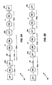
- Figure 1 is a block diagram illustrating a programmable logic device according to the present invention.
- Figure 2 is a block diagram of a logic cell used in a CLB based PLD architecture according to the prior art.
- Figure 3 is a logic cell with enhanced register functionality useful for better understanding the present invention.
- Figure 4 is a logic cell with register feedback useful for better understanding the present invention.
- Figures 5A and 5B are a block diagrams illustrating how register feedback aids in balancing delays between stages of a logic circuit design to reduce the overall propagation delays of the circuit.
- Figures 6A-6E are various implementations of a logic cell having improved logic functionality capabilities, and useful for better understanding the invention.
- Figures 7 is an embodiment of a logic cell of the present invention having register feedback and an input swap multiplexer.
- Figures 8A-8B is a logic cell capable of performing arithmetic on two bits in accordance with another implementation useful for understanding the invention.
- the PLD includes a plurality of Complex Logic Blocks (CLBs) 12 arranged in an array of rows and columns.
- CLBs Complex Logic Blocks
- Each CLB 12 includes a first slice 14A and a second slice 14B.
- the slices 14A of the CLBs 12 in a given column are interconnected by a first carry chain 16A, as designated by the carry-in (Cin) and carry-out (Cout) lines received and outputted by the slices 14A.
- the slices 14B are interconnected by a second carry chain 16B, as designated by the carry-in (Cin) and carry-out (Cout) lines received and outputted by the slices 14B.
- CLBs 12 are interconnected by a plurality of inter-CLB lines, as is well known in the art.
- CLB based PLDs having slices see for example the " Virtex-5 User Guide", UG190 (v3.0), February 2, 2007, published by Xilinx Corporation, San Jose, CA, pages 155-181 .
- Each slice 14 includes one or more logic cells. In one specific embodiment, each slice 14 includes four logic cells. In other embodiments, either more or fewer logic cells may be used per slice 14. In alternative embodiments for example, one to three, or five through sixteen or more logic cells may be included per CLB 14. In general, the number of specific logic cells in a CLB is arbitrary, and should not be construed as limiting the present invention.
- the logic cell 20 includes a six-input Look Up Table 22, an arithmetic logic circuit 24, two output multiplexers 26A and 26B, and an output register 28.
- the six input Look Up Table 22 includes two five-input Look Up Tables 30A and 30B, each configured to receive the same set of inputs D1 through D5, and a Look Up Table output multiplexer 32, which is configured to receive a sixth input D6.
- the Look Up Table 22 can be configured as either a single six-input Look Up Table capable of generating a single logic function "06", or two five-input logic functions designated F1(D1, D2, D3, D4, D5) and F2(D1, D2, D3, D4, D5) respectively.
- the arithmetic circuit 24 is configured to implement arithmetic logic functions, such as counters and shifter registers.
- the arithmetic circuit 24 is configured to receive a seventh input (DX) and a carry-in (Cin) from the logic cell below. In response, the arithmetic circuit generates a SUM signal and a carry out signal (Cout), which is provided to the cell above.
- the output multiplexer 26A generates a non-registered output (DMUX) selected from inputs (06, O5, SUM and Cout).
- the output multiplexer 26B selects from inputs (06, O5, SUM, Cout, and DX).
- the register 28 generates a registered output (DQ) from the input selected by multiplexer 26B.
- a third output (D) is derived from the Look Up Table output multiplexer 34 (06).
- Figure 3 is a logic cell with enhanced register functionality.
- the logic cell 36 is similar to the cell 20, except it additionally includes a second output register 38, output multiplexer 40, and a scan-chain 42.
- the output multiplexer 26B is configured to receive (scan-in, 06 and Cout), while the multiplexer 40 is configured to receive (DQ, O5, SUM, and DX).
- the second output register is configured to generate output (DQ1), the value of which is determined by the selection of multiplexer 40.
- the scan-chain 42 in Figure 3 allows the output of one register (i.e., 28) to be provided as an input to the next register (i.e., 38).
- the register 28 receives the "scan-in” signal from the above cell, whereas the register 38 provides the "scan-out” signal to the next cell.
- the enhanced register functionality of logic cells 36 provides a number of advantages over conventional cells, such as that illustrated in Figure 2 .
- the scan-chain 42 through the registers 28 and 38 allows greater functionality, such as pipelining and/or the creation of shift registers, between cells. This feature was not possible in the prior cell.
- the partitioning of the outputs among the two registers 28 and 38 also provides greater flexibility in register packing, which is the ability to efficiently place or "pack" more logic into a given cell.
- the output signals generated by the logic cell 36 in Figures 3 are merely exemplary.
- the output signals may be partitioned in any arbitrary way among the output registers.
- the output signals do not have to be limited to those specifically identified above. Rather, the output signals can be selected from generic signals, such as outputs of the Look Up Tables of the cell, a sum, carry-out signal, or any other signal generated by the arithmetic circuit 24, or any of the inputs to the logic cell.
- a logic cell 56 with register feedback is shown which is useful for understanding the invention.
- the logic cell 56 is similar to that of Figure 2 , except it includes a multiplexer 58 and a feedback path 60 between the (DQ) output of the register 28 and the multiplexer 58.
- the multiplexer 58 receives two inputs, D1 and DQ. Accordingly, the registered output of the cell 56 can be selectively provided as an input to both five-input Look Up Tables 30A and 30B.
- the multiplexer 58 is shown coupled to the input D1, it should be noted that the multiplexer 58 can be used to "swap" the registered output (DQ) for any of the logic cell inputs D 1 through D6.
- Pipelining is common in circuit design technique. With pipelining, a complex circuit is broken down or partitioned into a plurality of clocked pipelined stages. At each stage, the circuit performs a specific operation. With each clock cycle, the results of each stage are transitioned to the next stage.
- the speed (i.e., frequency) or clock cycle of the pipelined circuit is dictated by the longest propagation path between any two stages in the pipeline. For example, if a number of stages have a propagation delay of 5 nanoseconds, but one stage has a delay of 10 nanoseconds, then the entire circuit must operate at the 10 nanosecond rate. Higher speed performance can therefore be achieved if a better balance of the delays at the various stages of the circuit can be achieved.
- FIG. 5A a block diagram 65 illustrating how register feedback aids in balancing delays between pipelined stages of a logic circuit.
- the first stage A has a circuit 68 with a 5 nanosecond delay followed by register 28a.
- the second stage B has a long wire 69 with a 5 nanosecond delay, a first circuit 68b with a 5 nanosecond delay and a second circuit 68b with another 5 nanosecond delay, followed by a register 28b.
- the third stage C has two circuits 68c with a combined 10 nanosecond delay and a register 28c.
- the delay of the long wire 69 can be made to occur before (i.e., to the left of) the register 28a, rather than after (i.e., or to the right of the register).
- This shifting of the delay associated with wire 69 is logically illustrated in Figure 5B .
- the delay at each of the three stages has been balanced with each being 10 nanoseconds. Consequently, as illustrated in this example, the register feedback 60 can be used to improve the clock speed or frequency at which the logic circuit operates, thereby improving performance.
- Figures 6A-6E show various implementations of a logic cell of the present invention having improved logic functionality capabilities.
- the two Look Up Tables in the cell 20 of Figure 2 have limited flexibility, as each is limited in receiving the same inputs (D1, D2, D3, D4, D5).
- Figures 6A - 6E in contrast show various implementations where different combinations of inputs can be provided to the two five-input Look Up Tables 30A and 30B respectively. This flexibility aid in improving the density or "packing" as more logic can be squeezed into two Look Up Tables 30A and 30B capable of operating on different inputs, as opposed to operating only on the same set of inputs.
- the Look Up Table 30A receives inputs (D1A, D2, D3, D4, D5) and generates function F1 (D1A, D2, D3, D4, D5).
- Look Up Table 30B receives (D1B, D2, D3, D4, D5) and generates function F2 (D1B, D2, D3, D4, D5).
- the D1 input to the two Look Up Tables 30A and 30B is therefore different. This arrangement improves flexibility when the two Look Up Tables 30A and 30B are used in a fractured mode. For example, since 30A and 30B are sharing only four inputs, they can be configured as two independent three-input Look Up Tables, or two four-input Look Up Tables, with only two common inputs. It should be noted that the use of different inputs for D1 is only exemplary. Any of the inputs D 1 through D5 can be different in accordance with this implementation.
- the Look Up Table 30A receives inputs (D1A, D2A, D3, D4, D5) and generates function F.1 (D1A, D2A, D3, D4, D5).
- Look Up Table 30B receives (D1B, D2B, D3, D4, D5) and generates function F2 (D1B, D2B, D3, D4, D5).
- the D1 and D2 inputs to the two Look Up Tables 30A and 30B is therefore different. This arrangement also improves flexibility when the two Look Up Tables 30A and 30B are used in a fractured mode. For example, since 30A and 30B can each implement four-input Look Up Tables with two common inputs. It should be noted that the use of different inputs for D1 and D2 is only exemplary. Any two of the inputs D1 through D5 can be different in accordance with this implementation.
- Figure 6C is similar to Figure 6B with the Look Up Table 30A receiving inputs (D1A, D2A, D3, D4, D5) and Look Up Table 30B receiving inputs (D1B, D2B, D3, D4, D5).
- a swap multiplexer 62, AND gate 64 and a programming bit "R" are provided to control the multiplexer 62 and gate 64.
- the swap multiplexer 62 allows either the input D5 or D6 to be provided to the fifth input of Look Up Table 30A.
- the output of the AND gate 64 will force the multiplexer 32 to select the function F1 from the Look Up Table 30A.
- the Look Up Table 30A will always be selected by multiplexer 32. With the R bit set, Look Up Table 30A generates the function F1 (D6, D3, D2A, D1A) and 30B generates the function F2 (D5, D4, D2B, D1B). When the R bit is reset, then the 30A and 30B implement two five-input Look Up Tables with two common inputs respectively.
- Figure 6D is similar to Figure 6B , except it includes a swap multiplexer 68 coupled to receive the DX or D1A inputs.
- the Look Up Table 30B receives either DX or D1A, instead of D1B as illustrated in Figure 6B .
- the swap multiplexer 68 it allows the DX input to be substituted for the otherwise shared input D1, allowing the 30A and 30B to be fractured into two four-input Look Up Tables.
- F1 is therefore (D5, D3, D2A, D1A) and F2 is (D5, D4, D2B, DX).
- Figure 6E is the combination of Figures 6C and 6D .
- 30A and 30B can be configured as two five-input Look Up Tables with common inputs, or two fractured Look Up Tables generating F1(D6, D4, D3, D2A, D1A) and F2(D5, D3, D4, D2B, DX) respectively.
- Figure 7 is an embodiment of a logic cell of the present invention having register feedback and an input swap multiplexer.
- This embodiment is essentially the combination Figures 5A including register feedback 60 and the swap multiplexer 68 of Figure 6D .
- the swap multiplexer receives three inputs, including D2A, DX and the register feedback 60.
- 30A and 30B are capable of generating two 5-LUT functions, the lower of which is able to use the feedback register driven by DX as one of it's inputs.
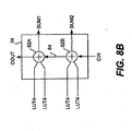
- Figure 8A is a cell having an arithmetic logic circuit 24 capable of generating two sum outputs, SUM1 and SUM2.
- the first SUM1 signal is derived by the addition from two signals from the first Look Up Table 30A
- the second SUM2 is generated from two signals from the second Look Up Table 30B.
- a five-input Look Up Table is essentially two four-input multiplexers and a select multiplexer that is controlled by the fifth input.
- the diagram of Figure 8 shows two four-input Look Up Tables and a multiplexer for elements 30A and 30B respectively.
- the non-registered output and output multiplexer of the cell are not shown.
- Figure 8B is a logic diagram illustrating the arithmetic logic circuit 24 of Figure 8A .
- the SUM1 signal is generated by a first adder 82A from the sum of two four-input Look Up Tables
- the signal SUM2 is generated by a second adder 82b from the sum of a second two four-input Look Up Tables.
- a carry signal 84 is provided between the two adders 84B and 84A.
- a programmable logic device includes a plurality of CLBs arranged in rows and columns of an array and a plurality of inter-CLB lines interconnecting the CLBs of the array.
- Each of the plurality of CLBs has a first slice of logic cells and a second slice of logic cells, wherein the first slice of logic cells and the second slice of logic cells of the CLBs in a given column of the array are interconnected by a first carry chain and a second carry chain respectively.
- One of the logic cells includes a first Look Up Table for implanting logic functions on a first set of five inputs provided to the one logic cell; and a second Look Up Table for implementing logic functions on a second set of five inputs provided to the one logic cell, wherein the first set of inputs and the second set of inputs contain similar inputs, but at least one of the inputs in the first set and the second set are different.
- the first set of inputs may comprise (D1A, D2, D3, D4 and D5) and the first Look Up Table may generate a logic function F1 (D1A, D2, D3, D4 and D5) and the second set of inputs may comprise (D1B, D2, D3, D4 and D5) and the second Look Up Table may generate a logic function F2 (D1B, D2, D3, D4 and D5) respectively.
- the first set of inputs may comprise (D1A, D2A, D3, D4 and D5) and the first Look Up Table generates a logic function F1 (D1A, D2A, D3, D4 and D5) and the second set of inputs comprises (D1B, D2B, D3, D4 and D5) and the second Look Up Table generates a logic function F2 (D1B, D2B, D3, D4 and D5) respectively.
- the first Look Up Table is a five-input Look Up Table and the second Look Up Table is also a five-input Look Up Table, the one logic cell further comprising a Look Up Table output multiplexer configured to receive the outputs of the first and the second Look Up Tables and a sixth input for controlling the output of the Look Up Table output multiplexer.
- the programmable logic device further comprises a programmable select multiplexer coupled to a selected one of the first set of inputs and the sixth input, the select multiplexer being configured to programmably select either the select one of the first set of inputs or the sixth input as an input to the first Look Up Table.
- the programmable logic device further may comprise a configurable bit used to control the programmable select multiplexer and the Look Up Table multiplexer so that when the sixth input is selected as an input to the first Look Up Table, the Look Up Table output multiplexer is configured to select the second Look Up Table.
- the programmable logic device further may comprise a seventh input to the one logic cell and a select multiplexer configured to selectively provide either the seventh input or one of the second set of inputs to the second Look Up Table.
- the programmable logic device of the invention further comprises a register feedback signal from a register of the one logic cell and a select multiplexer configured to selectively provide either the register feedback signal or one of the second set of inputs to the second Look Up Table.
Landscapes
- Physics & Mathematics (AREA)
- Mathematical Physics (AREA)
- Engineering & Computer Science (AREA)
- Computer Hardware Design (AREA)
- Computing Systems (AREA)
- General Engineering & Computer Science (AREA)
- Logic Circuits (AREA)
- Design And Manufacture Of Integrated Circuits (AREA)
Applications Claiming Priority (2)
| Application Number | Priority Date | Filing Date | Title |
|---|---|---|---|
| US11/751,392 US7394287B1 (en) | 2007-05-21 | 2007-05-21 | Programmable logic device having complex logic blocks with improved logic cell functionality |
| EP08009415A EP2001133B1 (en) | 2007-05-21 | 2008-05-21 | A programmable logic device having complex logic blocks with improved logic cell functionality |
Related Parent Applications (2)
| Application Number | Title | Priority Date | Filing Date |
|---|---|---|---|
| EP08009415.4 Division | 2008-05-21 | ||
| EP08009415A Division EP2001133B1 (en) | 2007-05-21 | 2008-05-21 | A programmable logic device having complex logic blocks with improved logic cell functionality |
Publications (3)
| Publication Number | Publication Date |
|---|---|
| EP2391011A2 EP2391011A2 (en) | 2011-11-30 |
| EP2391011A3 EP2391011A3 (en) | 2012-03-14 |
| EP2391011B1 true EP2391011B1 (en) | 2015-01-28 |
Family
ID=39561130
Family Applications (3)
| Application Number | Title | Priority Date | Filing Date |
|---|---|---|---|
| EP11174213.6A Active EP2391011B1 (en) | 2007-05-21 | 2008-05-21 | A programmable logic device having complex logic blocks with improved logic cell functionality |
| EP11174212.8A Active EP2391010B1 (en) | 2007-05-21 | 2008-05-21 | A programmable logic device having complex logic blocks with improved logic cell functionality |
| EP08009415A Active EP2001133B1 (en) | 2007-05-21 | 2008-05-21 | A programmable logic device having complex logic blocks with improved logic cell functionality |
Family Applications After (2)
| Application Number | Title | Priority Date | Filing Date |
|---|---|---|---|
| EP11174212.8A Active EP2391010B1 (en) | 2007-05-21 | 2008-05-21 | A programmable logic device having complex logic blocks with improved logic cell functionality |
| EP08009415A Active EP2001133B1 (en) | 2007-05-21 | 2008-05-21 | A programmable logic device having complex logic blocks with improved logic cell functionality |
Country Status (4)
| Country | Link |
|---|---|
| US (2) | US7394287B1 (https=) |
| EP (3) | EP2391011B1 (https=) |
| JP (2) | JP4896074B2 (https=) |
| CN (1) | CN101312347B (https=) |
Families Citing this family (17)
| Publication number | Priority date | Publication date | Assignee | Title |
|---|---|---|---|---|
| US7394287B1 (en) * | 2007-05-21 | 2008-07-01 | Altera Corporation | Programmable logic device having complex logic blocks with improved logic cell functionality |
| US7592835B2 (en) * | 2007-12-28 | 2009-09-22 | Intel Corporation | Co-processor having configurable logic blocks |
| WO2010058248A1 (en) * | 2008-11-24 | 2010-05-27 | Freescale Semiconductor, Inc. | Logic built-in self-test system and method for applying a logic built-in self-test to a device under test |
| US9762246B2 (en) | 2011-05-20 | 2017-09-12 | Semiconductor Energy Laboratory Co., Ltd. | Semiconductor device with a storage circuit having an oxide semiconductor |
| US9442478B2 (en) * | 2011-11-30 | 2016-09-13 | Infineon Technologies Ag | Systems, circuits and a method for generating a configurable feedback |
| CN103259529B (zh) * | 2012-02-17 | 2016-03-16 | 京微雅格(北京)科技有限公司 | 一种采用跳跃进位链的集成电路 |
| US8860458B2 (en) | 2012-07-20 | 2014-10-14 | Altera Corporation | Integrated circuits with logic regions having input and output bypass paths for accessing registers |
| US9158882B2 (en) * | 2013-12-19 | 2015-10-13 | Netspeed Systems | Automatic pipelining of NoC channels to meet timing and/or performance |
| HRP20140883A2 (hr) * | 2014-09-16 | 2016-03-25 | Željko Božić | Višeslojni univerzalni logički sklopovi |
| CN105874714B (zh) * | 2014-12-11 | 2020-02-14 | 京微雅格(北京)科技有限公司 | 支持多模式可配置的六输入查找表结构和fpga器件 |
| CN105874713B (zh) * | 2014-12-11 | 2019-03-08 | 京微雅格(北京)科技有限公司 | 一种可扩展可配置的逻辑元件和fpga器件 |
| WO2017040049A1 (en) * | 2015-09-01 | 2017-03-09 | Flex Logix Technologies, Inc. | Block memory layout and architecture for programmable logic ic, and method of operating same |
| CN113904677B (zh) * | 2021-10-11 | 2022-07-01 | 北京汤谷软件技术有限公司 | 一种可定制多种输入的查找表电路及fpga新型阵列结构 |
| US12249987B2 (en) | 2021-12-31 | 2025-03-11 | Lattice Semiconductor Corporation | Programmable look-up table systems and methods |
| CN115495044B (zh) * | 2022-09-01 | 2023-08-29 | 深圳市紫光同创电子有限公司 | 一种进位逻辑电路 |
| CN116719772B (zh) * | 2023-05-06 | 2024-10-01 | 深圳市紫光同创电子有限公司 | 可编程逻辑电路 |
| CN116820015B (zh) * | 2023-08-29 | 2023-11-17 | 灵动集成电路南京有限公司 | 具有灵活可配置逻辑模块的微控制器 |
Citations (1)
| Publication number | Priority date | Publication date | Assignee | Title |
|---|---|---|---|---|
| US20050275427A1 (en) * | 2004-06-10 | 2005-12-15 | Man Wang | Field programmable gate array logic unit and its cluster |
Family Cites Families (25)
| Publication number | Priority date | Publication date | Assignee | Title |
|---|---|---|---|---|
| US5274581A (en) * | 1992-05-08 | 1993-12-28 | Altera Corporation | Look up table implementation of fast carry for adders and counters |
| US5481206A (en) * | 1993-09-02 | 1996-01-02 | Xilinx, Inc. | Circuit for fast carry and logic |
| WO1995022205A1 (en) * | 1994-02-15 | 1995-08-17 | Xilinx, Inc. | Tile based architecture for fpga |
| US5550843A (en) * | 1994-04-01 | 1996-08-27 | Xilinx, Inc. | Programmable scan chain testing structure and method |
| US5689195A (en) * | 1995-05-17 | 1997-11-18 | Altera Corporation | Programmable logic array integrated circuit devices |
| US5646545A (en) * | 1995-08-18 | 1997-07-08 | Xilinx, Inc. | Time multiplexed programmable logic device |
| JPH09181598A (ja) * | 1995-12-18 | 1997-07-11 | At & T Corp | フィールドプログラマブルゲートアレイ |
| US5963050A (en) * | 1997-02-26 | 1999-10-05 | Xilinx, Inc. | Configurable logic element with fast feedback paths |
| US6396302B2 (en) | 1999-02-25 | 2002-05-28 | Xilinx, Inc. | Configurable logic element with expander structures |
| US6150838A (en) * | 1999-02-25 | 2000-11-21 | Xilinx, Inc. | FPGA configurable logic block with multi-purpose logic/memory circuit |
| US6961741B2 (en) * | 2001-02-15 | 2005-11-01 | Stmicroelectronics Ltd. | Look-up table apparatus to perform two-bit arithmetic operation including carry generation |
| US7076595B1 (en) * | 2001-05-18 | 2006-07-11 | Xilinx, Inc. | Programmable logic device including programmable interface core and central processing unit |
| US6833730B1 (en) * | 2002-08-30 | 2004-12-21 | Xilinx, Inc. | PLD configurable logic block enabling the rapid calculation of sum-of-products functions |
| US6943580B2 (en) | 2003-02-10 | 2005-09-13 | Altera Corporation | Fracturable lookup table and logic element |
| US7185035B1 (en) | 2003-10-23 | 2007-02-27 | Altera Corporation | Arithmetic structures for programmable logic devices |
| US7167021B1 (en) * | 2003-11-24 | 2007-01-23 | Altera Corporation | Logic device logic modules having improved arithmetic circuitry |
| JP4664311B2 (ja) * | 2003-12-29 | 2011-04-06 | ザイリンクス インコーポレイテッド | カスケード接続するdspスライスを備えた集積回路 |
| US7167022B1 (en) * | 2004-03-25 | 2007-01-23 | Altera Corporation | Omnibus logic element including look up table based logic elements |
| US20050218929A1 (en) * | 2004-04-02 | 2005-10-06 | Man Wang | Field programmable gate array logic cell and its derivatives |
| US7030652B1 (en) * | 2004-04-23 | 2006-04-18 | Altera Corporation | LUT-based logic element with support for Shannon decomposition and associated method |
| US7218140B1 (en) * | 2005-06-14 | 2007-05-15 | Xilinx, Inc. | Integrated circuit having fast interconnect paths between carry chain multiplexers and lookup tables |
| US7274214B1 (en) * | 2005-06-14 | 2007-09-25 | Xilinx, Inc. | Efficient tile layout for a programmable logic device |
| US7268584B1 (en) * | 2005-07-28 | 2007-09-11 | Altera Corporation | Adder circuitry for a programmable logic device |
| US7330052B2 (en) * | 2005-09-22 | 2008-02-12 | Altera Corporation | Area efficient fractureable logic elements |
| US7394287B1 (en) | 2007-05-21 | 2008-07-01 | Altera Corporation | Programmable logic device having complex logic blocks with improved logic cell functionality |
-
2007
- 2007-05-21 US US11/751,392 patent/US7394287B1/en active Active
-
2008
- 2008-05-14 JP JP2008127612A patent/JP4896074B2/ja not_active Expired - Fee Related
- 2008-05-20 CN CN200810100719.7A patent/CN101312347B/zh active Active
- 2008-05-21 EP EP11174213.6A patent/EP2391011B1/en active Active
- 2008-05-21 EP EP11174212.8A patent/EP2391010B1/en active Active
- 2008-05-21 EP EP08009415A patent/EP2001133B1/en active Active
- 2008-05-22 US US12/125,824 patent/US7675319B2/en active Active
-
2011
- 2011-11-08 JP JP2011244455A patent/JP5559129B2/ja not_active Expired - Fee Related
Patent Citations (1)
| Publication number | Priority date | Publication date | Assignee | Title |
|---|---|---|---|---|
| US20050275427A1 (en) * | 2004-06-10 | 2005-12-15 | Man Wang | Field programmable gate array logic unit and its cluster |
Also Published As
| Publication number | Publication date |
|---|---|
| EP2001133A2 (en) | 2008-12-10 |
| JP4896074B2 (ja) | 2012-03-14 |
| EP2391010A2 (en) | 2011-11-30 |
| EP2391010A3 (en) | 2012-03-21 |
| US7394287B1 (en) | 2008-07-01 |
| EP2391011A3 (en) | 2012-03-14 |
| EP2001133A3 (en) | 2008-12-24 |
| US7675319B2 (en) | 2010-03-09 |
| CN101312347A (zh) | 2008-11-26 |
| EP2391011A2 (en) | 2011-11-30 |
| JP2012055004A (ja) | 2012-03-15 |
| US20080290898A1 (en) | 2008-11-27 |
| JP5559129B2 (ja) | 2014-07-23 |
| CN101312347B (zh) | 2014-09-03 |
| EP2001133B1 (en) | 2012-10-31 |
| EP2391010B1 (en) | 2014-11-19 |
| JP2008289151A (ja) | 2008-11-27 |
Similar Documents
| Publication | Publication Date | Title |
|---|---|---|
| EP2391011B1 (en) | A programmable logic device having complex logic blocks with improved logic cell functionality | |
| US8878567B1 (en) | Omnibus logic element | |
| US8601424B1 (en) | Programmable logic device having logic elements with dedicated hardware to configure look up tables as registers | |
| US7075333B1 (en) | Programmable circuit optionally configurable as a lookup table or a wide multiplexer | |
| US5821774A (en) | Structure and method for arithmetic function implementation in an EPLD having high speed product term allocation structure | |
| EP2645574B1 (en) | Integrated circuits with multi-stage logic regions | |
| US8072238B1 (en) | Programmable logic device architecture with the ability to combine adjacent logic elements for the purpose of performing high order logic functions | |
| US7164290B2 (en) | Field programmable gate array logic unit and its cluster | |
| US20020079921A1 (en) | Configurable logic block for PLD with logic gate for combining output with another configurable logic block | |
| EP1944869B1 (en) | Variable sized soft memory macros in structured cell arrays, and related methods | |
| CN101312346B (zh) | 具有带改进的寄存器性能的逻辑模块的可编程逻辑器件 | |
| US7417456B2 (en) | Dedicated logic cells employing sequential logic and control logic functions | |
| US7268584B1 (en) | Adder circuitry for a programmable logic device | |
| US9235498B1 (en) | Circuits for and methods of enabling the modification of an input data stream | |
| US7812633B1 (en) | Apparatus and method for the arithmetic over-ride of look up table outputs in a programmable logic device | |
| US7856467B2 (en) | Integrated circuit including at least one configurable logic cell capable of multiplication | |
| US12008337B2 (en) | Multi-input configurable logic cell with configurable output region | |
| US7336099B1 (en) | Multiplexer including addition element |
Legal Events
| Date | Code | Title | Description |
|---|---|---|---|
| AC | Divisional application: reference to earlier application |
Ref document number: 2001133 Country of ref document: EP Kind code of ref document: P |
|
| AK | Designated contracting states |
Kind code of ref document: A2 Designated state(s): DE GB |
|
| PUAI | Public reference made under article 153(3) epc to a published international application that has entered the european phase |
Free format text: ORIGINAL CODE: 0009012 |
|
| PUAL | Search report despatched |
Free format text: ORIGINAL CODE: 0009013 |
|
| AK | Designated contracting states |
Kind code of ref document: A3 Designated state(s): DE GB |
|
| RIC1 | Information provided on ipc code assigned before grant |
Ipc: H03K 19/177 20060101AFI20120207BHEP |
|
| 17P | Request for examination filed |
Effective date: 20120912 |
|
| 17Q | First examination report despatched |
Effective date: 20121121 |
|
| GRAP | Despatch of communication of intention to grant a patent |
Free format text: ORIGINAL CODE: EPIDOSNIGR1 |
|
| INTG | Intention to grant announced |
Effective date: 20140814 |
|
| GRAS | Grant fee paid |
Free format text: ORIGINAL CODE: EPIDOSNIGR3 |
|
| GRAA | (expected) grant |
Free format text: ORIGINAL CODE: 0009210 |
|
| AC | Divisional application: reference to earlier application |
Ref document number: 2001133 Country of ref document: EP Kind code of ref document: P |
|
| AK | Designated contracting states |
Kind code of ref document: B1 Designated state(s): DE GB |
|
| REG | Reference to a national code |
Ref country code: GB Ref legal event code: FG4D |
|
| REG | Reference to a national code |
Ref country code: DE Ref legal event code: R096 Ref document number: 602008036587 Country of ref document: DE Effective date: 20150312 |
|
| REG | Reference to a national code |
Ref country code: DE Ref legal event code: R097 Ref document number: 602008036587 Country of ref document: DE |
|
| PLBE | No opposition filed within time limit |
Free format text: ORIGINAL CODE: 0009261 |
|
| STAA | Information on the status of an ep patent application or granted ep patent |
Free format text: STATUS: NO OPPOSITION FILED WITHIN TIME LIMIT |
|
| 26N | No opposition filed |
Effective date: 20151029 |
|
| PGFP | Annual fee paid to national office [announced via postgrant information from national office to epo] |
Ref country code: GB Payment date: 20160426 Year of fee payment: 9 |
|
| GBPC | Gb: european patent ceased through non-payment of renewal fee |
Effective date: 20170521 |
|
| PG25 | Lapsed in a contracting state [announced via postgrant information from national office to epo] |
Ref country code: GB Free format text: LAPSE BECAUSE OF NON-PAYMENT OF DUE FEES Effective date: 20170521 |
|
| P01 | Opt-out of the competence of the unified patent court (upc) registered |
Effective date: 20230531 |
|
| PGFP | Annual fee paid to national office [announced via postgrant information from national office to epo] |
Ref country code: DE Payment date: 20250423 Year of fee payment: 18 |