EP2391008A2 - Schutzvorrichtung und Verfahren für elektronische Vorrichtungen - Google Patents
Schutzvorrichtung und Verfahren für elektronische Vorrichtungen Download PDFInfo
- Publication number
- EP2391008A2 EP2391008A2 EP11167318A EP11167318A EP2391008A2 EP 2391008 A2 EP2391008 A2 EP 2391008A2 EP 11167318 A EP11167318 A EP 11167318A EP 11167318 A EP11167318 A EP 11167318A EP 2391008 A2 EP2391008 A2 EP 2391008A2
- Authority
- EP
- European Patent Office
- Prior art keywords
- terminal
- coupled
- solid state
- voltage
- transistor
- Prior art date
- Legal status (The legal status is an assumption and is not a legal conclusion. Google has not performed a legal analysis and makes no representation as to the accuracy of the status listed.)
- Granted
Links
Images

Classifications
-
- H—ELECTRICITY
- H03—ELECTRONIC CIRCUITRY
- H03K—PULSE TECHNIQUE
- H03K17/00—Electronic switching or gating, i.e. not by contact-making and –breaking
- H03K17/08—Modifications for protecting switching circuit against overcurrent or overvoltage
- H03K17/082—Modifications for protecting switching circuit against overcurrent or overvoltage by feedback from the output to the control circuit
- H03K17/0822—Modifications for protecting switching circuit against overcurrent or overvoltage by feedback from the output to the control circuit in field-effect transistor switches
-
- H—ELECTRICITY
- H03—ELECTRONIC CIRCUITRY
- H03K—PULSE TECHNIQUE
- H03K17/00—Electronic switching or gating, i.e. not by contact-making and –breaking
- H03K17/51—Electronic switching or gating, i.e. not by contact-making and –breaking characterised by the components used
- H03K17/78—Electronic switching or gating, i.e. not by contact-making and –breaking characterised by the components used using opto-electronic devices, i.e. light-emitting and photoelectric devices electrically- or optically-coupled
Definitions
- Embodiments of this invention relate to electronic devices having input terminals and/or output terminals, and, more particularly, to a circuit and method for protecting the electronic device from being damaged by excessive voltages applied to the input terminals and/or output terminals.
- Electronic devices often have input terminals that receive signals of various types or output terminals from which output signals of various types are provided. In fact, many electronic devices have both such input terminals and output terminals.
- Such electronic device include internal circuitry or components that may be damaged if a voltage having a large magnitude is applied to an input terminal or an output terminal.
- electronic test equipment may have output terminals from which precision output voltages or currents are provided. The magnitude of these output voltages or currents may be relatively low, and the circuits or components that provide these output voltages or currents may be damaged if a relatively large voltage or current, such as an AC supply voltage, it applied to the output terminals.
- the resistance of a circuit component connected between the terminals may be measured by coupling a specific current between the terminals and then measuring the voltage between the terminals. If current from a circuit supplying current to the terminals is diverted to a current sensing component coupled between the terminals, the resistance measurement may be in error.
- a protection system for an electronic device includes a current limiting device and a solid state relay coupled in series between an input or output terminal and the electronic device.
- the solid state relay may include an optotransistor coupled between the terminal and the electronic device in series with the current limiting device, and a light emitting diode optically coupled to the optotransistor.
- the current limiting device may be implemented with one or more enhancement mode field effect transistors.
- a voltage detection circuit detects a voltage applied to the terminal having a magnitude that is greater than a specific value. The detection circuit then causes the solid state relay to close. For example, the voltage detection circuit may apply a voltage to a light emitting diode used in a solid state relay thereby causing current to flow through the first light emitting diode.
- a protection circuit comprising: a first terminal; a second terminal; a current limiting device coupled to the first terminal; a solid state relay having switch terminals coupled in series with the current limiting device between the first terminal and the second terminal, the solid state relay having a control terminal and being configured to selectively decouple the first and second switch terminals from each other responsive to a control signal applied to the control terminal; and a detection circuit coupled to the solid state relay and the first terminal and being configured to detect a voltage applied to the first terminal having a magnitude that is greater than a specific value, the detection circuit being configured to apply the control signal to the solid state relay responsive to detecting the voltage having a magnitude greater than the specific value.
- the protection circuit may further comprise a relay having a relay contact coupled in series with the solid state relay between the first and second terminals, the relay further having a relay coil coupled to the detection circuit to receive a signal from the detection circuit responsive to detecting the voltage having a magnitude greater than the specific value to open the relay contact.
- the current limiting device may comprise at least one depletion mode field effect transistor.
- the current limiting device comprises: a first depletion mode field effect transistor having a drain coupled to the first terminal, a source coupled to the solid state relay, and a gate; and a second depletion mode field effect transistor having a drain coupled to the second terminal, a source coupled to the solid state relay and to the gate of the first depletion mode field effect transistor, and a gate coupled to the source of the source of the first depletion mode field effect transistor.
- the solid state relay comprises: a light emitting diode coupled to the control terminal of the solid state relay; and an opto-transistor optically coupled to the light emitting diode, the optotransistor being coupled between the switch terminals of the solid state relay.
- the detection circuit comprises a voltage detector coupled to the second terminal and configured to detect a voltage larger than a particular level, the voltage detector being configured to apply the control signal to the solid state relay to decouple the first and second switch terminals from each other responsive to detecting a voltage larger than the particular level.
- the detection circuit comprises a circuit extending between a first connection to the first terminal and a second connection to the first terminal, the second connection being separated from the first connection by the current limiting device.
- the solid state relay comprises a first solid state relay
- the detection circuit comprises a second solid state relay having a pair of control terminals coupled between the first connection and the second connection, the second solid state relay further having a switch terminal coupled to the first solid state relay and configured to apply the control signal to the solid state relay responsive to a current flowing between the first connection and the second connection.
- the second solid state relay comprises: a light emitting diode coupled between the control terminals of the second solid state relay; and an opto transistor optically coupled to the light emitting diode of the second solid state relay and electrically coupled to the control terminal of the first solid state relay.
- the detection circuit comprises: a first light emitting diode having a cathode coupled to the first connection and an anode coupled to the second connection; a second light emitting diode having an anode coupled to the first connection and a cathode coupled to the second connection; a first opto-transistor optically coupled to the first light emitting diode, the first opto-transistor being coupled to the control input of the first solid state relay; and a second opto-transistor optically coupled to the second light emitting diode, the second opto-transistor being coupled to the control input of the first solid state relay.
- the first and second opto-transistors are coupled to the control input of the solid state relay through a circuit, comprising: a comparator having an input coupled to the first and second optotransistors and an output; and a latch having a latch input coupled to the output of the comparator and a latch output coupled to the control input of the solid state relay.
- the specific voltage that the detection circuit is configured to detect is dynamically adjustable by programming the detection circuit with different voltage detection levels.
- a system comprising: an electronic device having a device terminal; a system terminal; a current limiting device coupling the system terminal to the device terminal; a first opto-transistor coupled between the system terminal and the device terminal in series with the current limiting device; a first light emitting diode optically coupled to the first opto-transistor; and a detection circuit configured to detect a voltage applied to the system terminal having a magnitude that is greater than a specific value, the detection circuit being coupled to apply a voltage to the first light emitting diode to cause current to flow through the first light emitting diode responsive to detecting a voltage applied to the system terminal having a magnitude that is greater than a specific value.
- the current limiting device comprises: a first depletion mode field effect transistor having a drain coupled to the system terminal, a source coupled to a first terminal of the opto-transistor, and a gate; and a second depletion mode field effect transistor having a drain coupled to the device terminal, a source coupled to the gate of the first depletion mode field effect transistor and to a second terminal of the opto-transistor that is different from the first terminal of the opto-transistor, and a gate coupled to the source of the first depletion mode field effect transistor.
- the detection circuit comprises: a second light emitting diode having a cathode coupled to a first connection to the system terminal and having an anode coupled to a second connection to the system terminal, the second connection being separated from the first connection by the current limiting device; a third light emitting diode having an anode coupled to the first connection and a cathode coupled to the second connection; a second opto-transistor optically coupled to the second light emitting diode, the second opto-transistor being coupled to the first light emitting diode; and a third opto-transistor optically coupled to the third light emitting diode, the third opto-transistor being coupled to the first light emitting diode.
- the second and third opto-transistors are coupled to the first light emitting diode through a circuit, comprising: a comparator having an input coupled to the second and third opto-transistors and an output; and a latch having a latch input coupled to the output of the comparator and a latch output coupled to the first light emitting diode.
- the electronic device comprises an electrical testing device configured to selectively couple a current or voltage to the device terminal having a plurality of different magnitudes, and wherein the detection circuit is configured to be programmable to adjust the specific voltage that the detection circuit is configured to detect as a function of the current or voltage that the electronic device couples to the device terminal.
- the system may further comprise a relay having a relay contact coupled between the system terminal and the device terminal, the relay further having a relay coil coupled to the detection circuit to receive a signal from the detection circuit responsive to detecting the voltage having a magnitude greater than the specific value to open the relay contact.
- a method of protecting an electronic device from a voltage applied to a terminal comprising: coupling the terminal to the electronic device thorough an opto-transistor; optically coupling the opto-transistor to a light emitting diode; detecting a voltage applied to the terminal having a magnitude that is greater than a specific value; limiting the flow of current from the terminal and the electronic device; and in response to detecting the voltage having a magnitude that is greater than a specific value, interrupting an electrical connection between the terminal and the electronic device by causing current to flow though the light emitting diode.
- the act of detecting the voltage having a magnitude that is greater than a specific value comprises detecting a voltage differential in a path through which the terminal is coupled to the electronic device.
- the act of limiting the flow of current from the terminal and the electronic device comprises coupling the terminal to the electronic device by at least one depletion mode field effect transistor.
- the protection circuit 10 includes a pair of output terminals 14, 16, one of which is coupled to the drain of a first n-channel depletion mode field effect transistor ("FET") 18 through a contact 20a of a relay 20.
- FET field effect transistor
- a coil that controls the conductive state of the contact 20a will be described below.
- a source of the FET 18 is coupled to a source of a second n-channel depletion mode FET 24.
- Respective gates of the FET's 18, 24 are both coupled to the sources of the FET's 18, 22.
- a drain of the FET 24 is coupled to both a terminal 28 that may be coupled to an output terminal of an electronic device (not shown) and a voltage detection circuit 30.
- the voltage detection circuit 30 detects a voltage that is larger than a specific voltage, and then applies a signal to a coil 20b of the relay 20, which then resets the relay to open the relay contact 20a.
- An electronic device coupled to the terminal 28 may then protected from a voltage that is larger than the specific voltage that may be applied between the terminals 14, 16.
- the FET's 18, 24, being depletion mode FET's, are conductive until the source-to-gate voltage reaches a threshold voltage for the FET's.
- the FET's 18, 24 since the respective sources and gates of the FET's 18, 24 are coupled to each other, the FET's 18, 24 never become non-conductive. Instead, the FET's 18, 24 initially act as resistors when the applied voltage is increased so that the current through the FET's 18, 24 increases accordingly. However, when the FET reaches saturation, the current through the FET's 18, 24 remains constant. The FET's 18, 24 thus act as current limiters until the voltage detection circuit 30 resets the relay 20 to open the relay contact 20a.
- the current limiting effect of the FET's 18, 24 protects an internal circuit or component connected to the terminal 28 until the relay contact 20a is opened.
- the FET's 18, 24 may become damaged or destroyed before the relay contact 20a can be opened.
- the voltage detector 30 may be able to very quickly detect a significant voltage applied to the terminals 14, 16
- one relay 20 used in the prior art protection circuit 10 may require about 7ms for the contact 20a to be opened.
- the FET's 18, 24 may be damaged or destroyed if the applied voltage increases sufficiently during these 7 ms.
- the prior art protection circuit 10 may be inadequate in many instances.
- a protection circuit 100 according to one example of the invention is shown in Figure 2 .
- the protection circuit 100 uses many of the same components that are used in the protection circuit 10 of Figure 1 . Therefore, in the interest of brevity and clarity, the same reference numerals will be used, and an explanation of the function and operation of these components will not be repeated.
- the protection circuit 100 may differ from the protection circuit 10 by including a solid state relay 120 to interrupt the flow of current through the output terminal 14 before the FET's 18, 24 can become damaged.
- the solid state relay 120 may include a light-emitting diode (“LED") 124 coupled between a pair of control terminals 126 one of which is coupled to the output of the voltage detection circuit 30 through a resistor 128.
- LED light-emitting diode
- the solid state relay 120 may also include a depletion mode n-channel opto-FET 130 that is controlled by light from the LED 124.
- the opto-FET 130 is coupled between a pair of switch terminals 132, which are coupled to the sources of respective ones of the FET's 18, 24.
- the solid state relay 120 may have a response time that is significantly faster than the response time of the relay 20, and is sufficiently fast to terminate the flow of current through the FET's 18, 24 before the FETs become damaged.
- the magnitude of the voltage that the solid state relay 120 can handle may be less than the magnitude of the voltage that the FET's 18, 24 can handle.
- the FET's 18, 24 may have a maximum operating voltage of about 650 volts while the opto-FET 130 may have an operating voltage of only about 60 volts.
- the current may initially flow through the FET's 18, 24 and the solid state relay 120.
- the FET's 18, 24 will then limit the current flow to a level that prevents the voltage drop across the solid state relay 120 from exceeding its maximum operating voltage.
- the voltage detector 30 will quickly sense the relatively high voltage, and will then apply a signal to the LED 124.
- the LED 124 in the solid state relay 120 will then couple light to the opto-FET 130, which causes it to turn OFF.
- the solid state relay 120 may terminate the flow of current through the FET's 18, 24 before the FET's can be damaged because it may respond much more quickly than the relay 20. Additionally, the relay 20 will respond before an excessive voltage is placed across the solid state relay 120.
- the detection voltage at which the voltage detector 30 applies a signal to the relay coil 20b may be fixed in some embodiments, in other embodiments the detection voltage may be dynamic. More specifically, the voltage detector may be programmed with a detection voltage that varies as a function of variations in the voltage that is applied between the terminals 14, 16 during normal operation so that the detection voltage is always greater than the normal operating voltage.
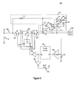
- FIG. 3 Another embodiment of a protection circuit 150 according is shown in Figure 3 .
- the protection circuit 150 may use many of the same components that are used in the embodiment of the protection circuit 100 shown in Figure 2 . Therefore, in the interest of brevity and clarity, the same reference numerals will again be used, and an explanation of the function and operation of these components will not be repeated.
- the protection circuit 150 may differ from the protection circuit 100 by avoiding the use of any circuit component that may divert current from the current path between an electronic device 160 to be protected and the terminal 14.
- the electronic device 160 may be, for example, an electrical testing device that provides a current having a specific magnitude to the terminal 14.
- the protection circuit 150 includes a voltage detector circuit 170 that includes a resistor 172 coupling the terminal 14 to control terminal 173 a second solid state relay 176 and a third solid state relay 180.
- the control terminal 173 of the second solid state relay 176 is connected to the anode of an LED 174
- the control terminal 173 of the third solid state relay 180 is connected to the cathode of an LED 178.
- Each solid state relay 176, 180 may include an opto-transistor, such as an opto NPN transistor 184, 186, respectively, that is optically coupled to the respective LED 176, 178.
- the cathode of the LED 174 and the anode of the LED 178 are connected to respective control terminals 173 of the first and second solid state relays 176, 178, respectively, which are in turn connected back to the conductive path extending between the terminal 14 and the electronic device 160.
- the respective collectors of the transistors 184, 186 may be coupled through a switch terminal 188 to a supply voltage, such as 5 volts, and the respective emitters of the transistors 184, 186 are coupled through another switch terminal 188 to an input of a comparator 190 and a resistor 192, which is coupled to ground.
- An output of the comparator 190 is coupled to a set ("S") input of a latch 194, which has an output coupled to an input of a first inverter 196 and an input of a second inverter 198.
- An output of the first inverter 196 is coupled to the relay coil 20b, and an output of the second inverter 198 is coupled to the LED 124 of the solid state relay 120.
- the current may initially flow through the FET's 18, 24 and the solid state relay 120. However, the FET's 18, 24 will then limit the current flow to a level that prevents the voltage drop across the solid state relay 120 from exceeding its maximum operating voltage.
- one of the LED's 174, 178 in the solid state relays 176, 180, respectively will be conductive to turn ON its respective transistor 184, 186 when the current through the LED reaches a specific level .
- the magnitude of the voltage applied to the terminals 14, 16 at which the transistors 184, 186 turn ON may be set by the selection of the value of the resistor 172.
- the latch 194 will be set by the comparator 190 to drive the output of the inverter 196 low and cause current to flow through the LED 124 in the solid state relay 120.
- a low at the output of the inverter 198 may reset the relay 20 to open the relay contact 20a after the delay of the relay 20.
- the current flowing through the LED 124 will then illuminate the LED, thereby turning OFF the LED 124 in the solid state relay 120.
- the solid state relay 120 may terminate the flow of current through the FET's 18, 24 before the FET's can be damaged because it can respond much more quickly than the relay 20. Additionally, the relay 20 will respond before an excessive voltage is placed across the solid state relay 120.
- any current flowing through the resistor 172 and one of the LED's 174, 176 is returned to the current path between the terminal 14 and the electronic device 160 so that the detection circuit 170 does not divert current flowing from the electronic device 160 to the terminal 14 or vice versa.
Landscapes
- Electronic Switches (AREA)
- Emergency Protection Circuit Devices (AREA)
Applications Claiming Priority (1)
| Application Number | Priority Date | Filing Date | Title |
|---|---|---|---|
| US12/788,025 US8582265B2 (en) | 2010-05-26 | 2010-05-26 | Protection circuit and method for electronic devices |
Publications (3)
| Publication Number | Publication Date |
|---|---|
| EP2391008A2 true EP2391008A2 (de) | 2011-11-30 |
| EP2391008A3 EP2391008A3 (de) | 2015-12-09 |
| EP2391008B1 EP2391008B1 (de) | 2022-11-30 |
Family
ID=44736145
Family Applications (1)
| Application Number | Title | Priority Date | Filing Date |
|---|---|---|---|
| EP11167318.2A Active EP2391008B1 (de) | 2010-05-26 | 2011-05-24 | Schutzvorrichtung und Verfahren für elektronische Vorrichtungen |
Country Status (3)
| Country | Link |
|---|---|
| US (1) | US8582265B2 (de) |
| EP (1) | EP2391008B1 (de) |
| CN (1) | CN102263397B (de) |
Cited By (1)
| Publication number | Priority date | Publication date | Assignee | Title |
|---|---|---|---|---|
| CN120433119A (zh) * | 2025-04-27 | 2025-08-05 | 芯洲科技(北京)股份有限公司 | 芯片测试中继电器的保护电路和电子芯片 |
Families Citing this family (15)
| Publication number | Priority date | Publication date | Assignee | Title |
|---|---|---|---|---|
| EP2779346B1 (de) * | 2013-03-15 | 2020-05-27 | Fairchild Semiconductor Corporation | Verfahren und Vorrichtung mit einem Strombegrenzer |
| US9136691B2 (en) * | 2013-08-08 | 2015-09-15 | Tyco Electronics Corporation | Solid state relay protective device |
| KR101604916B1 (ko) * | 2014-08-06 | 2016-03-25 | 엘에스산전 주식회사 | 입력 채널별 절연 구조 및, 상기 구조를 포함하는 온도 제어 장치 및, 온도 제어 방법 |
| US10276321B2 (en) | 2015-04-06 | 2019-04-30 | Atom Power, Inc. | Dynamic coordination of protection devices in electrical distribution systems |
| DE102015109167B3 (de) * | 2015-06-10 | 2016-08-11 | Weetech Gmbh | Bidirektionaler MOSFET-Schalter und Multiplexer |
| CN112366104B (zh) * | 2016-03-01 | 2024-08-20 | 原子动力公司 | 混合式气隙和固态断路器 |
| US10725105B2 (en) * | 2017-09-29 | 2020-07-28 | Keithley Instruments, Llc | Current leakage and charge injection mitigating solid state switch |
| US10630069B2 (en) | 2017-10-03 | 2020-04-21 | Atom Power, Inc. | Solid-state circuit interrupter and arc inhibitor |
| US11037749B2 (en) | 2018-05-04 | 2021-06-15 | Atom Power, Inc. | Selective coordination of solid-state circuit breakers and mechanical circuit breakers in electrical distribution systems |
| WO2020252121A1 (en) | 2019-06-13 | 2020-12-17 | Atom Power, Inc. | Distribution panel for intelligently controlled solid-state circuit breakers |
| US11791620B2 (en) | 2019-09-03 | 2023-10-17 | Atom Power, Inc. | Solid-state circuit breaker with self-diagnostic, self-maintenance, and self-protection capabilities |
| KR20220058919A (ko) | 2019-09-03 | 2022-05-10 | 아톰 파워, 인크. | 자가-진단, 자가-유지보수 및 자가-보호 기능을 갖는 고체 상태 회로 차단기 |
| WO2022125492A1 (en) | 2020-12-08 | 2022-06-16 | Atom Power, Inc. | Electric vehicle charging system and method |
| US12377751B2 (en) | 2020-12-08 | 2025-08-05 | Atom Power, Inc. | Electric vehicle supply equipment unit configured in an EV charging system |
| CN115084335A (zh) * | 2021-03-12 | 2022-09-20 | 深圳市光科全息技术有限公司 | Micro LED芯片的转移方法 |
Family Cites Families (15)
| Publication number | Priority date | Publication date | Assignee | Title |
|---|---|---|---|---|
| US3708672A (en) * | 1971-03-29 | 1973-01-02 | Honeywell Inf Systems | Solid state relay using photo-coupled isolators |
| JPS5650448B2 (de) * | 1974-03-08 | 1981-11-28 | ||
| US4158150A (en) * | 1978-01-10 | 1979-06-12 | Amf Incorporated | Solid state relay with zero crossover feature |
| US5777836A (en) * | 1994-04-01 | 1998-07-07 | U.S. Robotics Mobile Communications Corp. | Line current protection circuit and method for use with a PCMCIA-architecture modem card |
| US5457591A (en) | 1995-01-12 | 1995-10-10 | Loral Federal Systems Company | Current overload protection circuit |
| US5729418A (en) * | 1996-08-29 | 1998-03-17 | Supertex, Inc. | High voltage current limiting protection circuit and method therefor |
| DE29823936U1 (de) | 1998-08-14 | 2000-01-27 | Siemens AG, 80333 München | Bipolarer Strombegrenzer |
| US6519127B1 (en) * | 2000-10-03 | 2003-02-11 | Compaq Computer Corporation | Solid state safety relay |
| JP2002232282A (ja) * | 2001-01-31 | 2002-08-16 | Matsushita Electric Works Ltd | 半導体リレー及びその製造方法 |
| US20030151478A1 (en) * | 2001-10-02 | 2003-08-14 | Dejan Radosavljevic | Protection device with lockout test |
| JP4416585B2 (ja) * | 2004-07-06 | 2010-02-17 | 三洋電機株式会社 | 車両用の電源装置 |
| US20060098373A1 (en) * | 2004-11-09 | 2006-05-11 | Fultec Semiconductors, Inc. | Intelligent transient blocking unit |
| JP4345839B2 (ja) * | 2007-04-16 | 2009-10-14 | 株式会社デンソー | 電力変換装置 |
| FR2930091B1 (fr) * | 2008-04-09 | 2011-10-28 | Schneider Electric Ind Sas | Systeme a relais statique comprenant deux transistors de type jfet en serie |
| MX2010012772A (es) * | 2008-05-23 | 2010-12-21 | Fisher Controls Int | Circuito de deteccion de multi-voltaje opto-aislador. |
-
2010
- 2010-05-26 US US12/788,025 patent/US8582265B2/en active Active
-
2011
- 2011-05-24 EP EP11167318.2A patent/EP2391008B1/de active Active
- 2011-05-25 CN CN201110147931.0A patent/CN102263397B/zh active Active
Non-Patent Citations (1)
| Title |
|---|
| None |
Cited By (1)
| Publication number | Priority date | Publication date | Assignee | Title |
|---|---|---|---|---|
| CN120433119A (zh) * | 2025-04-27 | 2025-08-05 | 芯洲科技(北京)股份有限公司 | 芯片测试中继电器的保护电路和电子芯片 |
Also Published As
| Publication number | Publication date |
|---|---|
| EP2391008A3 (de) | 2015-12-09 |
| CN102263397B (zh) | 2014-11-12 |
| US20110292556A1 (en) | 2011-12-01 |
| US8582265B2 (en) | 2013-11-12 |
| EP2391008B1 (de) | 2022-11-30 |
| CN102263397A (zh) | 2011-11-30 |
Similar Documents
| Publication | Publication Date | Title |
|---|---|---|
| EP2391008B1 (de) | Schutzvorrichtung und Verfahren für elektronische Vorrichtungen | |
| CN109425816B (zh) | 测试mos功率开关 | |
| CN101652927B (zh) | 用于负载电路的过电流保护装置 | |
| JP4473927B2 (ja) | 短絡保護装置 | |
| KR101291367B1 (ko) | 온도 검출 회로 | |
| CN105337272B (zh) | 静电释放保护电路 | |
| US9800239B2 (en) | Electronic circuit | |
| US9941717B2 (en) | Battery device | |
| US20180145668A1 (en) | Voltage clamping circuit | |
| US11114880B2 (en) | Current regulating circuit and power supply management circuit including the same | |
| EP3442019A1 (de) | Leistungsmodul | |
| TW201611486A (zh) | 用於電子裝置之保護裝置及方法 | |
| CN110718894B (zh) | 低压断路器和方法 | |
| US20040125528A1 (en) | Active transient suppression apparatus for potentially explosive environments | |
| US7619864B1 (en) | Regulator short-circuit protection circuit and method | |
| CN100553132C (zh) | 电源装置 | |
| CN103259247A (zh) | 保护电路和自动化组件 | |
| US10564205B2 (en) | Voltage abnormality detection circuit and semiconductor device | |
| JP7445894B2 (ja) | 漏電検出装置 | |
| US20150288349A1 (en) | Switch device | |
| CN108267648B (zh) | 具有静电防护功能的检测设备 | |
| US7498864B2 (en) | Electronic fuse for overcurrent protection | |
| US11362504B2 (en) | Over current sensing scheme for switch applications | |
| CN104836565A (zh) | 可快速切换栅极电位的输出缓冲器及静电防护电路 | |
| US11171477B2 (en) | Turn off circuit for protection switch |
Legal Events
| Date | Code | Title | Description |
|---|---|---|---|
| 17P | Request for examination filed |
Effective date: 20110524 |
|
| AK | Designated contracting states |
Kind code of ref document: A2 Designated state(s): AL AT BE BG CH CY CZ DE DK EE ES FI FR GB GR HR HU IE IS IT LI LT LU LV MC MK MT NL NO PL PT RO RS SE SI SK SM TR |
|
| AX | Request for extension of the european patent |
Extension state: BA ME |
|
| PUAI | Public reference made under article 153(3) epc to a published international application that has entered the european phase |
Free format text: ORIGINAL CODE: 0009012 |
|
| RIC1 | Information provided on ipc code assigned before grant |
Ipc: H03K 17/78 20060101ALI20150622BHEP Ipc: H03K 17/082 20060101AFI20150622BHEP |
|
| PUAL | Search report despatched |
Free format text: ORIGINAL CODE: 0009013 |
|
| AK | Designated contracting states |
Kind code of ref document: A3 Designated state(s): AL AT BE BG CH CY CZ DE DK EE ES FI FR GB GR HR HU IE IS IT LI LT LU LV MC MK MT NL NO PL PT RO RS SE SI SK SM TR |
|
| AX | Request for extension of the european patent |
Extension state: BA ME |
|
| RIC1 | Information provided on ipc code assigned before grant |
Ipc: H03K 17/78 20060101ALI20151103BHEP Ipc: H03K 17/082 20060101AFI20151103BHEP |
|
| STAA | Information on the status of an ep patent application or granted ep patent |
Free format text: STATUS: EXAMINATION IS IN PROGRESS |
|
| 17Q | First examination report despatched |
Effective date: 20190704 |
|
| GRAP | Despatch of communication of intention to grant a patent |
Free format text: ORIGINAL CODE: EPIDOSNIGR1 |
|
| STAA | Information on the status of an ep patent application or granted ep patent |
Free format text: STATUS: GRANT OF PATENT IS INTENDED |
|
| INTG | Intention to grant announced |
Effective date: 20220621 |
|
| GRAS | Grant fee paid |
Free format text: ORIGINAL CODE: EPIDOSNIGR3 |
|
| GRAA | (expected) grant |
Free format text: ORIGINAL CODE: 0009210 |
|
| STAA | Information on the status of an ep patent application or granted ep patent |
Free format text: STATUS: THE PATENT HAS BEEN GRANTED |
|
| AK | Designated contracting states |
Kind code of ref document: B1 Designated state(s): AL AT BE BG CH CY CZ DE DK EE ES FI FR GB GR HR HU IE IS IT LI LT LU LV MC MK MT NL NO PL PT RO RS SE SI SK SM TR |
|
| REG | Reference to a national code |
Ref country code: CH Ref legal event code: EP Ref country code: GB Ref legal event code: FG4D |
|
| REG | Reference to a national code |
Ref country code: AT Ref legal event code: REF Ref document number: 1535482 Country of ref document: AT Kind code of ref document: T Effective date: 20221215 Ref country code: DE Ref legal event code: R096 Ref document number: 602011073478 Country of ref document: DE |
|
| REG | Reference to a national code |
Ref country code: IE Ref legal event code: FG4D |
|
| REG | Reference to a national code |
Ref country code: LT Ref legal event code: MG9D |
|
| REG | Reference to a national code |
Ref country code: NL Ref legal event code: MP Effective date: 20221130 |
|
| PG25 | Lapsed in a contracting state [announced via postgrant information from national office to epo] |
Ref country code: SE Free format text: LAPSE BECAUSE OF FAILURE TO SUBMIT A TRANSLATION OF THE DESCRIPTION OR TO PAY THE FEE WITHIN THE PRESCRIBED TIME-LIMIT Effective date: 20221130 Ref country code: PT Free format text: LAPSE BECAUSE OF FAILURE TO SUBMIT A TRANSLATION OF THE DESCRIPTION OR TO PAY THE FEE WITHIN THE PRESCRIBED TIME-LIMIT Effective date: 20230331 Ref country code: NO Free format text: LAPSE BECAUSE OF FAILURE TO SUBMIT A TRANSLATION OF THE DESCRIPTION OR TO PAY THE FEE WITHIN THE PRESCRIBED TIME-LIMIT Effective date: 20230228 Ref country code: LT Free format text: LAPSE BECAUSE OF FAILURE TO SUBMIT A TRANSLATION OF THE DESCRIPTION OR TO PAY THE FEE WITHIN THE PRESCRIBED TIME-LIMIT Effective date: 20221130 Ref country code: FI Free format text: LAPSE BECAUSE OF FAILURE TO SUBMIT A TRANSLATION OF THE DESCRIPTION OR TO PAY THE FEE WITHIN THE PRESCRIBED TIME-LIMIT Effective date: 20221130 Ref country code: ES Free format text: LAPSE BECAUSE OF FAILURE TO SUBMIT A TRANSLATION OF THE DESCRIPTION OR TO PAY THE FEE WITHIN THE PRESCRIBED TIME-LIMIT Effective date: 20221130 |
|
| REG | Reference to a national code |
Ref country code: AT Ref legal event code: MK05 Ref document number: 1535482 Country of ref document: AT Kind code of ref document: T Effective date: 20221130 |
|
| PG25 | Lapsed in a contracting state [announced via postgrant information from national office to epo] |
Ref country code: RS Free format text: LAPSE BECAUSE OF FAILURE TO SUBMIT A TRANSLATION OF THE DESCRIPTION OR TO PAY THE FEE WITHIN THE PRESCRIBED TIME-LIMIT Effective date: 20221130 Ref country code: PL Free format text: LAPSE BECAUSE OF FAILURE TO SUBMIT A TRANSLATION OF THE DESCRIPTION OR TO PAY THE FEE WITHIN THE PRESCRIBED TIME-LIMIT Effective date: 20221130 Ref country code: LV Free format text: LAPSE BECAUSE OF FAILURE TO SUBMIT A TRANSLATION OF THE DESCRIPTION OR TO PAY THE FEE WITHIN THE PRESCRIBED TIME-LIMIT Effective date: 20221130 Ref country code: IS Free format text: LAPSE BECAUSE OF FAILURE TO SUBMIT A TRANSLATION OF THE DESCRIPTION OR TO PAY THE FEE WITHIN THE PRESCRIBED TIME-LIMIT Effective date: 20230330 Ref country code: HR Free format text: LAPSE BECAUSE OF FAILURE TO SUBMIT A TRANSLATION OF THE DESCRIPTION OR TO PAY THE FEE WITHIN THE PRESCRIBED TIME-LIMIT Effective date: 20221130 Ref country code: GR Free format text: LAPSE BECAUSE OF FAILURE TO SUBMIT A TRANSLATION OF THE DESCRIPTION OR TO PAY THE FEE WITHIN THE PRESCRIBED TIME-LIMIT Effective date: 20230301 |
|
| PG25 | Lapsed in a contracting state [announced via postgrant information from national office to epo] |
Ref country code: NL Free format text: LAPSE BECAUSE OF FAILURE TO SUBMIT A TRANSLATION OF THE DESCRIPTION OR TO PAY THE FEE WITHIN THE PRESCRIBED TIME-LIMIT Effective date: 20221130 |
|
| PG25 | Lapsed in a contracting state [announced via postgrant information from national office to epo] |
Ref country code: SM Free format text: LAPSE BECAUSE OF FAILURE TO SUBMIT A TRANSLATION OF THE DESCRIPTION OR TO PAY THE FEE WITHIN THE PRESCRIBED TIME-LIMIT Effective date: 20221130 Ref country code: RO Free format text: LAPSE BECAUSE OF FAILURE TO SUBMIT A TRANSLATION OF THE DESCRIPTION OR TO PAY THE FEE WITHIN THE PRESCRIBED TIME-LIMIT Effective date: 20221130 Ref country code: EE Free format text: LAPSE BECAUSE OF FAILURE TO SUBMIT A TRANSLATION OF THE DESCRIPTION OR TO PAY THE FEE WITHIN THE PRESCRIBED TIME-LIMIT Effective date: 20221130 Ref country code: DK Free format text: LAPSE BECAUSE OF FAILURE TO SUBMIT A TRANSLATION OF THE DESCRIPTION OR TO PAY THE FEE WITHIN THE PRESCRIBED TIME-LIMIT Effective date: 20221130 Ref country code: CZ Free format text: LAPSE BECAUSE OF FAILURE TO SUBMIT A TRANSLATION OF THE DESCRIPTION OR TO PAY THE FEE WITHIN THE PRESCRIBED TIME-LIMIT Effective date: 20221130 Ref country code: AT Free format text: LAPSE BECAUSE OF FAILURE TO SUBMIT A TRANSLATION OF THE DESCRIPTION OR TO PAY THE FEE WITHIN THE PRESCRIBED TIME-LIMIT Effective date: 20221130 |
|
| PG25 | Lapsed in a contracting state [announced via postgrant information from national office to epo] |
Ref country code: SK Free format text: LAPSE BECAUSE OF FAILURE TO SUBMIT A TRANSLATION OF THE DESCRIPTION OR TO PAY THE FEE WITHIN THE PRESCRIBED TIME-LIMIT Effective date: 20221130 Ref country code: AL Free format text: LAPSE BECAUSE OF FAILURE TO SUBMIT A TRANSLATION OF THE DESCRIPTION OR TO PAY THE FEE WITHIN THE PRESCRIBED TIME-LIMIT Effective date: 20221130 |
|
| REG | Reference to a national code |
Ref country code: DE Ref legal event code: R097 Ref document number: 602011073478 Country of ref document: DE |
|
| PLBE | No opposition filed within time limit |
Free format text: ORIGINAL CODE: 0009261 |
|
| STAA | Information on the status of an ep patent application or granted ep patent |
Free format text: STATUS: NO OPPOSITION FILED WITHIN TIME LIMIT |
|
| 26N | No opposition filed |
Effective date: 20230831 |
|
| PG25 | Lapsed in a contracting state [announced via postgrant information from national office to epo] |
Ref country code: SI Free format text: LAPSE BECAUSE OF FAILURE TO SUBMIT A TRANSLATION OF THE DESCRIPTION OR TO PAY THE FEE WITHIN THE PRESCRIBED TIME-LIMIT Effective date: 20221130 |
|
| REG | Reference to a national code |
Ref country code: CH Ref legal event code: PL |
|
| PG25 | Lapsed in a contracting state [announced via postgrant information from national office to epo] |
Ref country code: MC Free format text: LAPSE BECAUSE OF FAILURE TO SUBMIT A TRANSLATION OF THE DESCRIPTION OR TO PAY THE FEE WITHIN THE PRESCRIBED TIME-LIMIT Effective date: 20221130 |
|
| REG | Reference to a national code |
Ref country code: BE Ref legal event code: MM Effective date: 20230531 |
|
| PG25 | Lapsed in a contracting state [announced via postgrant information from national office to epo] |
Ref country code: MC Free format text: LAPSE BECAUSE OF FAILURE TO SUBMIT A TRANSLATION OF THE DESCRIPTION OR TO PAY THE FEE WITHIN THE PRESCRIBED TIME-LIMIT Effective date: 20221130 Ref country code: LU Free format text: LAPSE BECAUSE OF NON-PAYMENT OF DUE FEES Effective date: 20230524 Ref country code: LI Free format text: LAPSE BECAUSE OF NON-PAYMENT OF DUE FEES Effective date: 20230531 Ref country code: CH Free format text: LAPSE BECAUSE OF NON-PAYMENT OF DUE FEES Effective date: 20230531 |
|
| REG | Reference to a national code |
Ref country code: IE Ref legal event code: MM4A |
|
| PG25 | Lapsed in a contracting state [announced via postgrant information from national office to epo] |
Ref country code: IE Free format text: LAPSE BECAUSE OF NON-PAYMENT OF DUE FEES Effective date: 20230524 |
|
| PG25 | Lapsed in a contracting state [announced via postgrant information from national office to epo] |
Ref country code: IE Free format text: LAPSE BECAUSE OF NON-PAYMENT OF DUE FEES Effective date: 20230524 |
|
| PG25 | Lapsed in a contracting state [announced via postgrant information from national office to epo] |
Ref country code: IT Free format text: LAPSE BECAUSE OF FAILURE TO SUBMIT A TRANSLATION OF THE DESCRIPTION OR TO PAY THE FEE WITHIN THE PRESCRIBED TIME-LIMIT Effective date: 20221130 Ref country code: BE Free format text: LAPSE BECAUSE OF NON-PAYMENT OF DUE FEES Effective date: 20230531 |
|
| PG25 | Lapsed in a contracting state [announced via postgrant information from national office to epo] |
Ref country code: BG Free format text: LAPSE BECAUSE OF FAILURE TO SUBMIT A TRANSLATION OF THE DESCRIPTION OR TO PAY THE FEE WITHIN THE PRESCRIBED TIME-LIMIT Effective date: 20221130 |
|
| PG25 | Lapsed in a contracting state [announced via postgrant information from national office to epo] |
Ref country code: BG Free format text: LAPSE BECAUSE OF FAILURE TO SUBMIT A TRANSLATION OF THE DESCRIPTION OR TO PAY THE FEE WITHIN THE PRESCRIBED TIME-LIMIT Effective date: 20221130 |
|
| PGFP | Annual fee paid to national office [announced via postgrant information from national office to epo] |
Ref country code: DE Payment date: 20250528 Year of fee payment: 15 |
|
| PGFP | Annual fee paid to national office [announced via postgrant information from national office to epo] |
Ref country code: GB Payment date: 20250520 Year of fee payment: 15 |
|
| PGFP | Annual fee paid to national office [announced via postgrant information from national office to epo] |
Ref country code: FR Payment date: 20250526 Year of fee payment: 15 |
|
| PG25 | Lapsed in a contracting state [announced via postgrant information from national office to epo] |
Ref country code: CY Free format text: LAPSE BECAUSE OF FAILURE TO SUBMIT A TRANSLATION OF THE DESCRIPTION OR TO PAY THE FEE WITHIN THE PRESCRIBED TIME-LIMIT; INVALID AB INITIO Effective date: 20110524 |
|
| PG25 | Lapsed in a contracting state [announced via postgrant information from national office to epo] |
Ref country code: HU Free format text: LAPSE BECAUSE OF FAILURE TO SUBMIT A TRANSLATION OF THE DESCRIPTION OR TO PAY THE FEE WITHIN THE PRESCRIBED TIME-LIMIT; INVALID AB INITIO Effective date: 20110524 |
|
| PG25 | Lapsed in a contracting state [announced via postgrant information from national office to epo] |
Ref country code: TR Free format text: LAPSE BECAUSE OF FAILURE TO SUBMIT A TRANSLATION OF THE DESCRIPTION OR TO PAY THE FEE WITHIN THE PRESCRIBED TIME-LIMIT Effective date: 20221130 |