EP2390933B1 - Semiconductor light emitting device - Google Patents
Semiconductor light emitting device Download PDFInfo
- Publication number
- EP2390933B1 EP2390933B1 EP20100186525 EP10186525A EP2390933B1 EP 2390933 B1 EP2390933 B1 EP 2390933B1 EP 20100186525 EP20100186525 EP 20100186525 EP 10186525 A EP10186525 A EP 10186525A EP 2390933 B1 EP2390933 B1 EP 2390933B1
- Authority
- EP
- European Patent Office
- Prior art keywords
- electrode
- layer
- major surface
- semiconductor layer
- light emitting
- Prior art date
- Legal status (The legal status is an assumption and is not a legal conclusion. Google has not performed a legal analysis and makes no representation as to the accuracy of the status listed.)
- Not-in-force
Links
Images


Classifications
-
- H—ELECTRICITY
- H01—ELECTRIC ELEMENTS
- H01L—SEMICONDUCTOR DEVICES NOT COVERED BY CLASS H10
- H01L33/00—Semiconductor devices with at least one potential-jump barrier or surface barrier specially adapted for light emission; Processes or apparatus specially adapted for the manufacture or treatment thereof or of parts thereof; Details thereof
- H01L33/36—Semiconductor devices with at least one potential-jump barrier or surface barrier specially adapted for light emission; Processes or apparatus specially adapted for the manufacture or treatment thereof or of parts thereof; Details thereof characterised by the electrodes
- H01L33/38—Semiconductor devices with at least one potential-jump barrier or surface barrier specially adapted for light emission; Processes or apparatus specially adapted for the manufacture or treatment thereof or of parts thereof; Details thereof characterised by the electrodes with a particular shape
- H01L33/385—Semiconductor devices with at least one potential-jump barrier or surface barrier specially adapted for light emission; Processes or apparatus specially adapted for the manufacture or treatment thereof or of parts thereof; Details thereof characterised by the electrodes with a particular shape the electrode extending at least partially onto a side surface of the semiconductor body
-
- H—ELECTRICITY
- H01—ELECTRIC ELEMENTS
- H01L—SEMICONDUCTOR DEVICES NOT COVERED BY CLASS H10
- H01L33/00—Semiconductor devices with at least one potential-jump barrier or surface barrier specially adapted for light emission; Processes or apparatus specially adapted for the manufacture or treatment thereof or of parts thereof; Details thereof
- H01L33/02—Semiconductor devices with at least one potential-jump barrier or surface barrier specially adapted for light emission; Processes or apparatus specially adapted for the manufacture or treatment thereof or of parts thereof; Details thereof characterised by the semiconductor bodies
- H01L33/14—Semiconductor devices with at least one potential-jump barrier or surface barrier specially adapted for light emission; Processes or apparatus specially adapted for the manufacture or treatment thereof or of parts thereof; Details thereof characterised by the semiconductor bodies with a carrier transport control structure, e.g. highly-doped semiconductor layer or current-blocking structure
Definitions
- Embodiments described herein relate generally to a semiconductor light emitting device.
- an n-side electrode and a p-side electrode are formed on one major surface side of the semiconductor layer.
- the planar surface area of the p-side electrode is increased without changing the chip size (the planar size)
- the planar surface area of the n-side electrode is relatively reduced. In the case where the planar surface area of the n-side electrode is reduced, the reliability may decrease due to current concentration in the n-side electrode.
- US 2009/0283787 A1 discloses light emitting diodes including a diode region having first and second opposing faces that include therein an n-type layer and a p-type layer, an anode contact and a cathode contact. The anode or cathode contacts may further provide a hybrid reflective structure on the first face for reflecting light emerging from the first face back into the first face.
- US2009/0289273 A1 discloses a light emitting device including a substrate serving as a carrier supporting an LED chip and separate chip and substrate sides. Two conductive traces electrically connect a first and second electrode layer of the LED chip which are formed along the chip side and the substrate side simultaneously.
- WO 2008/131736 A1 discloses an optoelectronic component comprising a semiconductor body with an active region that is suitable for generating radiation and two electric contacts situated on the semiconductor body. Each of the contacts which are electrically connected to the active region has a connection surface facing away from the semiconductor body and being situated on a connection side of the component. One side of the component which is not the connection side is covered with a reflective surface.
- US 2002/0017651 A1 discloses a light emitting diode arranged so that the rays emitted from an exciting element comprising a n-type semiconductor layer and a p-type semiconductor layer are converted by a wavelength converting element to white light which is then irradiated through molded resin.
- the wavelength converting element is provided on one surface of the exciting element and an insulating film is deposited on the other surface with interposition of a p-type ohmic electrode exhibiting a high reflectivity in UV wavelength band.
- the exciting element has its side surface covered with a n-type ohmic electrode exhibiting a high reflectivity in UV wavelength band.
- a semiconductor light emitting device includes a semiconductor layer, a first electrode, a second electrode, a first insulating layer, a first interconnect layer, a second interconnect layer, a first metal pillar, a second metal pillar, and a second insulating layer.
- the semiconductor layer includes a light emitting layer, a first major surface, and a second major surface opposite to the first major surface.
- the first electrode is provided on the second major surface of the semiconductor layer.
- the second electrode is provided on a side face of a portion of the semiconductor layer between the light emitting layer and the first major surface.
- the first insulating layer is provided on a side of the second major surface of the semiconductor layer.
- the first insulating layer has a first opening reaching the first electrode and a second opening reaching the second electrode provided on the side face.
- the first interconnect layer is provided in the first opening and on the first insulating layer on a side opposite to the second major surface to connect to the first electrode.
- the second interconnect layer is provided in the second opening and on the first insulating layer on the side opposite to the second major surface to connect to the second electrode provided on the side face.
- the second interconnect layer is provided on the side face of the portion of the semiconductor layer with interposing the second electrode.
- the first metal pillar is provided on a face of the first interconnect layer on a side opposite to the first electrode.
- the second metal pillar is provided on a face of the second interconnect layer on a side opposite to the second electrode.
- the second insulating layer covers a periphery of the first metal pillar and a periphery of the second metal pillar.
- FIG. 1A is a schematic cross-sectional view taken along A-A' line in FIG. 1B of a semiconductor light emitting device of a first embodiment.
- FIG. 1B is a schematic perspective view of a semiconductor layer 15 and electrodes 17 and 18 of the semiconductor light emitting device.
- a first major surface 15a of the semiconductor layer 15 is illustrated on the upper side; and in FIG. 1B , the first major surface 15a is illustrated on the lower side.
- the semiconductor layer 15 includes a first semiconductor layer 11 and a second semiconductor layer 13.
- the first semiconductor layer 11 is, for example, an n-type GaN layer that functions as a lateral current path.
- the conductivity type of the first semiconductor layer 11 is not limited to the n-type; and the conductivity type may be a p-type.
- the semiconductor layer 15 includes a light emitting layer (an active layer) 12 and, for example, a p-type GaN layer and an n-type GaN layer with the light emitting layer 12 interposed therebetween.
- the second semiconductor layer 13 is provided on the side opposite to the first major surface 15a. Light is mainly extracted from the first major surface 15a of the semiconductor layer 15.
- a second major surface side of the semiconductor layer 15 on the side opposite to the first major surface 15a is patterned into a recessed and protruding configuration; and an upper level portion 15b and a lower level portion 15c are provided on the second major surface side.
- the upper level portion 15b is positioned more on the upper level side than is the lower level portion 15c as viewed from the first major surface 15a.
- the upper level portion 15b includes the light emitting layer 12.
- the lower level portion 15c does not include the light emitting layer 12 and is provided in the portion between the light emitting layer 12 and the first major surface 15a.
- the p-side electrode 17 is provided as a first electrode on the second major surface of the upper level portion 15b (the surface of the second semiconductor layer 13).
- the n-side electrode 18 is provided as a second electrode on the second major surface of the lower level portion 15c (the surface of the first semiconductor layer 11).
- the n-side electrode 18 is provided also on a side face 15d of the lower level portion 15c.
- the n-side electrode 18 formed on the side face 15d and the n-side electrode 18 formed on the surface of the lower level portion 15c (the second major surface) are formed as a single body from the same material and are joined at the corner between the side face 15d and the surface of the lower level portion 15c.
- the n-side electrode 18 formed on the side face 15d encloses the outer circumference of the lower level portion 15c, that is, is formed to be continuously formed on the side face 15d.
- the surface area of the portion of the n-side electrode 18 provided on the side face 15d is greater than the surface area of the portion of the n-side electrode 18 provided on the second major surface.
- the n-side electrode 18 surrounds the side surfaces 15d of the n-type semiconductor layer 11.
- the p-side electrode 17 is formed on the surface of the upper level portion 15b in a region (a light emitting region) in the surface direction of the semiconductor layer 15 including the light emitting layer 12.
- the surface area of the p-side electrode 17 on the second major surface is greater than the surface area of the n-side electrode 18 formed on the surface (on the second major surface) of the lower level portion 15c.
- An insulating film 16 such as, for example, a silicon oxide film is provided on the side face of the upper level portion 15b; and the insulating film 16 covers the side face of the light emitting layer 12.
- the insulating film 16 is interposed between the p-side electrode 17 and the n-side electrode 18 to insulatively separate the p-side electrode 17 and the n-side electrode 18.
- the second major surface and the side face 15d of the semiconductor layer 15 are covered with an insulating layer (a first insulating layer) 19.
- the insulating layer 19 is, for example, a resin or a silicon oxide film.
- the face of the insulating layer 19 on the side opposite to the second major surface is planarized; a p-side interconnect layer 21 is provided on the face as a first interconnect layer; and an n-side interconnect layer 22 is provided on the face as a second interconnect layer.
- the face of the n-side interconnect layer 22 on the side opposite to the face of the n-side interconnect layer 22 connected to the n-side electrode 18 on the lower level portion 15c surface (the second major surface) is larger than the face connected to the n-side electrode 18 on the lower level portion 15c surface.
- the layout of the n-side interconnect layer 22 on the insulating layer 19 has a surface area greater than that of the n-side electrode 18 on the lower level portion 15c surface.
- the p-side interconnect layer 21 is provided also in a first opening 19a made in the insulating layer 19 to reach the p-side electrode 17; and the p-side interconnect layer 21 is connected to the p-side electrode 17.
- a second opening 19b is made in the insulating layer 19 to reach the n-side electrode 18.
- the second opening 19b is made to reach the n-side electrode 18 on the surface of the lower level portion 15c and is made in a portion beside the n-side electrode 18 formed on the side face 15d. Accordingly, the second opening 19b communicates with the n-side electrode 18 formed on the side face 15d.
- the n-side interconnect layer 22 is provided also in the second opening 19b. In other words, the n-side interconnect layer 22 is provided also in the portion beside the n-side electrode 18 formed on the side face 15d. Accordingly, the n-side interconnect layer 22 is connected to the n-side electrode 18 provided on the side face 15d and on the surface of the lower level portion 15c.
- the side face 15d is tapered with respect to the first major surface 15a and the second major surface.
- the width of the portion of the second opening 19b beside the side face 15d gradually increases from the first major surface 15a side toward the second major surface side. Therefore, the fillability of the n-side interconnect layer 22 into the portion beside the side face 15d is good; and the n-side interconnect layer 22 can be reliably connected to the n-side electrode 18 provided on the side face 15d.
- a p-side metal pillar 24 is provided as the first metal pillar on the face of the p-side interconnect layer 21 on the side opposite to the p-side electrode 17.
- An n-side metal pillar 25 is provided as a second metal pillar on the face of the n-side interconnect layer 22 on the side opposite to the n-side electrode 18 on the second major surface.
- the second insulating layer may be an inorganic layer.
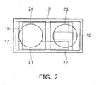
- FIG. 2 illustrates one example of a planar layout of the semiconductor layer 15, the p-side electrode 17, the n-side electrode 18, the p-side interconnect layer 21, the n-side interconnect layer 22, the p-side metal pillar 24, and the n-side metal pillar 25.
- FIG. 2 corresponds to a plan view of FIG. 1A as viewed from the lower face (the mounting surface) side.
- the resin layer 23 is not illustrated.
- the semiconductor light emitting device has a rectangular shape in a plan view, as shown in FIG. 2 .
- the layout of the p-side electrode 17 (shown a broken line in FIG. 2 ) on the second major surface of the semiconductor layer 15 has a surface area greater than that of the n-side electrode 18 (shown a broken line in FIG. 2 ).
- the p-side electrode 17 has a U shape.
- the n-side electrode 18 is provided between the opening of the U shape.
- the planar size of the insulating layer 19 is larger than the planar size of the semiconductor layer 15.
- the layout of the p-side interconnect layer 21 (shown a solid line in FIG. 2 ) is in a region of about one half of the lower face of the insulating layer 19, and the layout of the n-side interconnect layer 22 (shown a solid line in FIG. 2 ) is in a region of about the remaining half.
- the n-side interconnect layer 22 is formed to spread over the insulating layer 19 with a surface area greater than that of the portion of the n-side electrode 18 provided on the second major surface.
- the planar shape of the p-side interconnect layer 21 and the n-side interconnect layer 22 has a square shape or rectangular shape.
- the configurations of the metal pillars 24 and 25 are not limited to circular columnar configurations.
- the surface areas of the metal pillars 24 and 25 are same in a plan view.
- the metal pillars 24 and 25 are symmetric with a center line perpendicular to a longitudinal direction. Further the metal pillars 24 and 25 are symmetric with respect to a center in a plan view.
- Prismatic configurations, columnar configurations having other shapes, or pad configurations may be used.
- the first semiconductor layer 11 is electrically connected to the n-side metal pillar 25 via the n-side electrode 18 and the n-side interconnect layer 22.
- the second semiconductor layer 13 is electrically connected to the p-side metal pillar 24 via the p-side electrode 17 and the p-side interconnect layer 21.
- External terminals such as, for example, solder balls, metal bumps, etc., are provided on the lower end faces of the n-side metal pillar 25 and the p-side metal pillar 24 exposed from the resin layer 23.
- the semiconductor light emitting device is electrically connectable to an external circuit via the external terminals.
- the p-side interconnect layer 21 and the n-side interconnect layer 22 have a same planar shape as in FIG.2 . Further the surface areas of the p-side interconnect layer 21 and the n-side interconnect layer 22 are same.
- the p-side interconnect layer 21 and the n-side interconnect layer 22 are symmetric with a center line perpendicular to a longitudinal direction. Distances from the p-side interconnect layer 21 and the n-side interconnect layer 22 to short side lines (left outline and right outline in FIG.2 ) are same. Further the p-side interconnect layer 21 and the n-side interconnect layer 22 are symmetric with respect to a center in a plan view.
- the p-side interconnect layer 21 and the n-side interconnect layer 22 are symmetric with respect to a center and the metal pillars 24 and 25 are symmetric with respect to the center in a plan view. Therefore, the semiconductor light emitting device has a stability and rarely topples (inclines).
- Each of the thickness of the n-side metal pillar 25 and the thickness of the p-side metal pillar 24 is thicker than the thickness of a stacked body including the semiconductor layer 15, the n-side electrode 18, the p-side electrode 17, the insulating film 16, the insulating layer 19, the n-side interconnect layer 22, and the p-side interconnect layer 21.
- the aspect ratios (the ratio of the thickness to the planar size) of the metal pillars 24 and 25 are not limited to being 1 or more; and the ratios may be less than 1. In other words, the thicknesses of the metal pillars 24 and 25 may be smaller than the planar sizes thereof.
- the structure of this embodiment it is possible to maintain the mechanical strength even in the case where the semiconductor layer 15 is thin by making the n-side metal pillar 25, the p-side metal pillar 24, and the resin layer 23 thick.
- the n-side metal pillar 25 and the p-side metal pillar 24 can absorb and mitigate the stress applied to the semiconductor layer 15 via the external terminals.
- the materials of the n-side interconnect layer 22, the p-side interconnect layer 21, the n-side metal pillar 25, and the p-side metal pillar 24 may include copper, gold, nickel, silver, etc. Thereof, copper may be favorable because copper provides good thermal conductivity, high migration resistance, and excellent adhesion with insulating films.
- the resin layer 23, which performs the role of reinforcing the n-side metal pillar 25 and the p-side metal pillar 24, may be a substance having a coefficient of thermal expansion equal to or near that of the circuit board the like.
- Examples of such a resin layer 23 may include, for example, epoxy resin, silicone resin, fluorocarbon resin, etc.
- a fluorescent layer 26 is provided on the first major surface 15a of the semiconductor layer 15.
- the fluorescent layer 26 is capable of absorbing light from the light emitting layer 12 and emitting wavelength-converted light. Therefore, it is possible to emit mixed light of the light from the light emitting layer 12 and the wavelength-converted light of the fluorescent layer 26.
- the light emitting layer 12 is nitride-based, it is possible to obtain white light, lamp light, etc., as mixed-color light of blue light from the light emitting layer 12 and yellow light from, for example, the wavelength-converted light of a yellow fluorescent layer 26.
- the fluorescent layer 26 may have a configuration including multiple types of fluorescers (e.g., a red fluorescer and a green fluorescer).
- the light emitted by the light emitting layer 12 mainly travels through the first semiconductor layer 11, the first major surface 15a, and the fluorescent layer 26 to be emitted externally.
- the light emission surface area can be increased and the luminous efficacy can be increased by relatively increasing the planar surface area of the p-side electrode formed in the region including the light emitting layer.
- the planar surface area of the p-side electrode is increased without changing the chip size (the planar size)
- the planar surface area of the n-side electrode is relatively reduced.
- the reliability may decrease due to current concentration in the n-side electrode.
- the n-side electrode 18 is formed also on the side face 15d of the semiconductor layer 11.
- the surface area of the n-side electrode 18 contacting the first semiconductor layer 11 which is an n-type layer can be increased without reducing the surface area of the p-side electrode 17 on the second major surface.
- the surface area reduction of the p-side electrode 17 can be suppressed; the luminance can be increased; and the reliability can be increased by increasing the surface area of the n-side electrode 18.
- an increase of the chip size can be suppressed.
- the surface area of the p-side electrode 17 formed in the region including the light emitting layer 12 is greater than the surface area (the surface area on the second major surface) of the n-side electrode 18; and a larger light emitting region can be ensured.
- the p-side and the n-side are formed with substantially the same surface area; and current can be supplied efficiently.
- the n-side electrode 18 is made of a metal having light-shielding properties with respect to the light emitted by the light emitting layer 12. Accordingly, a structure is provided in which the side face 15d of the semiconductor layer 15 is covered with a light-shielding film. Therefore, light leakage from the side face 15d can be prevented; and uneven colors and uneven luminance can be suppressed. Further, the metal forming the n-side electrode 18 is reflective with respect to the light emitted by the light emitting layer. Therefore, the amount of the light reflected from the side face and extracted from the first major surface 15a side can be increased; and the luminance can be increased.
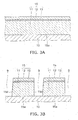
- the first semiconductor layer 11 is grown on the major surface of a substrate 10; and the light emitting layer 12 and the second semiconductor layer 13are grown thereupon.
- the semiconductor layer 15 may be formed by, for example, crystal growth on a sapphire substrate.
- a separating trench 9 is made to pierce the semiconductor layer 15 and reach the substrate 10 by, for example, Reactive Ion Etching (RIE) using a not-illustrated resist as a mask.
- RIE Reactive Ion Etching
- the separating trench 9 is made, for example, in a lattice configuration on the substrate 10 to multiply separate the semiconductor layer 15.
- the upper level portion 15b is formed on the second major surface side of the semiconductor layer 15 and positioned relatively in the upper level as viewed from the substrate 10; and the lower level portion 15c is formed on the second major surface side of the semiconductor layer 15 and positioned more in the lower level on the substrate 10 side than is the upper level portion 15b.
- the upper level portion 15b includes the light emitting layer 12; and the lower level portion 15c does not include the light emitting layer 12.
- the insulating film 16 made of a silicon oxide film or the like is formed on all exposed faces of the substrate 10 by, for example, chemical vapor deposition (CVD).
- the insulating film 16 covers exposed surface of the semiconductor layer 15 including the side face 15d and the second major surface of the semiconductor layer 15.
- the insulating film 16 also is formed on the side face and the bottom face of the separating trench 9.
- n-side electrode 18 is formed as illustrated in FIG. 5A on the exposed portions by, for example, sputtering. At this time, the portions other than the portions where the n-side electrode 18 is formed are covered with a not-illustrated mask such as a resist.
- the n-side electrode 18 includes, for example, a nickel film formed on the first semiconductor layer 11 side and an aluminum film stacked on the nickel film.
- an opening is selectively made in the insulating film 16 on the upper level portion 15b by, for example, wet etching to expose the upper face of the upper level portion 15b (the upper face of the second semiconductor layer 13).
- the p-side electrode 17 is formed as illustrated in FIG. 5B on the exposed portions by, for example, sputtering. At this time, the portions other than the portions where the p-side electrode 17 is formed are covered with a not-illustrated mask such as a resist.
- the p-side electrode 17 includes, for example, a nickel film formed on the second semiconductor layer 13 side and a gold film stacked on the nickel film.
- the p-side electrode 17 may be formed prior to the n-side electrode 18; or the p-side electrode 17 and the n-side electrode 18 may be formed simultaneously from the same material.
- the manufacturing step is provided in two steps as in FIGS. 5A and 5B .
- the manufacturing step may be one step. Namely, openings are formed in above a region to be formed the p-side electrode 17 and the n-side electrode 18 thereon.
- the insulating layer 19 is patterned as illustrated in FIG. 6A by, for example, wet etching to make the first opening 19a and the second opening 19b in the insulating layer 19.
- the insulating layer 19 is made of a resin such as, for example, polyimide having excellent patternability in ultra-fine patterns.
- the first opening 19a reaches the p-side electrode 17.
- the second opening 19b reaches the n-side electrode 18 formed on the upper face of the lower level portion 15c. Further, the second opening 19b is made in the portion beside the side face 15d and communicates with the n-side electrode 18 formed on the side face 15d.
- a continuous seed metal 20 is formed on the upper face of the insulating layer 19 and on the inner faces of the first opening 19a and the second opening 19b; and after forming a not-illustrated plating resist, Cu plating is performed using the seed metal 20 as a current path.
- the seed metal 20 includes, for example, Cu.
- the p-side interconnect layer 21 and the n-side interconnect layer 22 are formed selectively on the insulating layer 19.
- the p-side interconnect layer 21 and the n-side interconnect layer 22 are formed simultaneously by plating.
- the p-side interconnect layer 21 is formed also in the first opening 19a to connect to the p-side electrode 17.
- the n-side interconnect layer 22 is formed also in the second opening 19b to connect to the n-side electrode 18.
- the side face 15d is obtained when making the separating trench 9 described above referring to FIG. 3B .
- the separating trench 9 is made by RIE using a resist film selectively formed on the semiconductor layer 15 as a mask. At this time, the resist film is consumed isotropically in the film thickness direction and the planar direction; and the planar size of the resist film is reduced as the etching progresses. Accordingly, the width of the separating trench 9 gradually decreases in the depth direction. Accordingly, each of the cross-sectional configurations of the multiply subdivided semiconductor layer 15 on the substrate 10 is a trapezoidal configuration; and the side face 15d adjacent to the separating trench 9 is tapered with respect to the first major surface 15a and the second major surface.
- the width of the portion of the second opening 19b beside the side face 15d is wider upward; and it is possible to reliably form the seed metal 20 and the n-side interconnect layer 22 to the bottom of the second opening 19b.
- the plating resist used during the plating of the p-side interconnect layer 21 and the n-side interconnect layer 22 is removed by a chemical solution. Subsequently, another plating resist (not illustrated) is formed for forming the metal pillars; and Cu plating is performed using the seed metal 20 described above as a current path. Thereby, as illustrated in FIG. 7A , the p-side metal pillar 24 is formed above the p-side interconnect layer 21; and the n-side metal pillar 25 is formed above the n-side interconnect layer 22. The p-side metal pillar 24 and the n-side metal pillar 25 are formed simultaneously by plating.
- the plating resist for forming the metal pillars is removed by a chemical solution; and the exposed portions of the seed metal 20 also are removed. Thereby, the electrical connection between the p-side interconnect layer 21 and the n-side interconnect layer 22 via the seed metal 20 is divided.
- the p-side interconnect layer 21, the n-side interconnect layer 22, the p-side metal pillar 24, and the n-side metal pillar 25 are covered with the resin layer 23. Subsequently, the surface of the resin layer 23 is polished to expose the end faces (the upper faces) of the p-side metal pillar 24 and the n-side metal pillar 25.
- the substrate 10 is removed.
- the substrate 10 may be removed by, for example, laser lift-off. Specifically, laser light is irradiated from the backside of the substrate 10 toward the first semiconductor layer 11.
- the substrate 10 is permeable to laser light; and the laser light has a wavelength in the absorption region of the first semiconductor layer 11.
- the first semiconductor layer 11 proximal to the interface absorbs the energy of the laser light and decomposes.
- the first semiconductor layer 11 decomposes into Ga and nitrogen gas.
- a micro gap is formed between the substrate 10 and the first semiconductor layer 11 by the decomposition reaction; and the substrate 10 and the first semiconductor layer 11 separate. The irradiation of the laser light is performed over the entire wafer by performing multiply for each set region; and the substrate 10 is removed.
- the layer made of the resin and the metal is flexible, and the metal is formed by plating at near room temperature. Hence, the residual stress occurring with respect to the translucent substrate 10 is relatively low.
- the semiconductor layer made of GaN is separated by laser irradiation.
- the translucent substrate and the silicon substrate being different in thermal expansion coefficient are both rigid, and are bonded together at high temperature. Hence, a high residual stress remains between these substrates. Consequently, when the separation is started by laser irradiation, the residual stress is locally relieved from the separated portion and unfortunately causes cracks in the thin, brittle semiconductor layer.
- the residual stress is low, and the semiconductor layer 15 is separated in the state of being fixed to a flexible support.
- the device can be manufactured at high yield without trouble such as cracking in the semiconductor layer 15.
- the fluorescent layer 26 is formed on the first major surface 15a as illustrated in FIG. 7B ,
- the fluorescent layer 26 may be formed, for example, by coating a liquid resin in which phosphor particles are mixed by spin coating and then thermosetting.
- the substrate 10 By forming the fluorescent layer 26 after removing the substrate 10 from the first major surface 15a, the substrate 10 does not exist between the first major surface 15a and the fluorescent layer 26; and the light extraction efficiency can be increased.
- dicing is performed to obtain the singulated semiconductor light emitting device illustrated in FIG. 1A .
- the substrate 10 is already removed; and in the separating trench 9 which is the dicing region, the semiconductor layer 15 does not exist and the insulating layer 19 which is a resin is filled. Accordingly, the dicing is easy because the insulating layer 19, which is a resin, and the resin layer 23 are cut; and the productivity can be improved. Further, damage to the semiconductor layer 15 during the dicing can be avoided. Also, a structure is obtained after singulation in which the periphery of the device is covered with resin and protected.
- the singulated semiconductor light emitting device may have a single-chip structure including one semiconductor layer 15 or a multi-chip structure including multiple semiconductor layers 15.
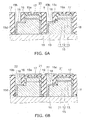
- FIG. 8A is a schematic cross-sectional view of a semiconductor light emitting device of a second embodiment.
- FIG. 8B is a schematic perspective view of the semiconductor layer 15 and the electrodes 17 and 18 of the semiconductor light emitting device.
- the first major surface 15a of the semiconductor layer 15 is illustrated on the upper side; and in FIG. 8B , the first major surface 15a is illustrated on the lower side.
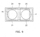
- FIG. 9 illustrates one example of a planar layout of the semiconductor layer 15 (shown as broken line in FIG. 9 ), the p-side electrode 17 (shown as broken line in FIG. 9 ), the p-side interconnect layer 21, the n-side interconnect layer 22, the p-side metal pillar 24, and the n-side metal pillar 25 of this embodiment.
- FIG. 9 corresponds to a plan view as viewed from the lower face (the mounting surface) side of FIG. 8A .
- the resin layer 23 is not illustrated.
- the n-side electrode 18 is formed on the side face 15d of the first semiconductor layer 11 between the first major surface 15a and the light emitting layer 12 of the semiconductor layer 15.
- the surface area reduction of the p-side electrode 17 can be suppressed; the luminance can be increased; and the reliability can be increased by increasing the surface area of the n-side electrode 18.
- the light leakage from the side face 15d can be prevented; and the uneven colors and the uneven luminance can be suppressed.
- the amount of light reflected by the side face and extracted from the first major surface 15a side can be increased; and the luminance can be increased.
- the n-side electrode 18 is not provided on the second major surface and is provided only on the side face 15d. Accordingly, as illustrated in FIG. 8B and FIG. 9 , the surface area of the p-side electrode 17 provided on the second major surface can be greater; and a larger light emitting region can be obtained. Thereby, the luminous efficacy can be increased. Because the processes described above and illustrated in FIG. 4A that expose the second major surface of the first semiconductor layer 11 can be omitted, cost reductions also are possible.
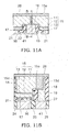
- FIG. 10A is a schematic perspective view of the semiconductor layer 15 and the electrodes 17 and 18 of a semiconductor light emitting device of a third embodiment.
- FIG. 10B corresponds to a plan view of FIG. 10A .
- FIG. 11A corresponds to a cross section along A-A of FIG. 10B .
- FIG. 11B corresponds to a cross section along B-B of FIG. 11A .
- FIG. 12 illustrates one example of a planar layout of the semiconductor layer 15, the p-side electrode 17, the n-side electrode 18, the p-side interconnect layer 21, the n-side interconnect layer 22, the p-side metal pillar 24, and the n-side metal pillar 25 of this embodiment.
- FIG. 12 corresponds to a plan view as viewed from the lower face (the mounting surface) side of FIG. 11B .
- the resin layer 23 is not illustrated.
- the layout of the p-side electrode 17 has a surface area greater than that of the n-side electrode 18.
- the n-side interconnect layer 22 is formed to spread over the insulating layer 19 with a surface area greater than that of the portion of the n-side electrode 18 provided on the second major surface.
- the n-side electrode 18 is formed on the side face 15d and the upper face (the second major surface) of the lower level portion 15c of the semiconductor layer 15.
- a trench 41 is formed in the lower level portion 15c.
- the trench 41 is formed from the second major surface of the lower level portion 15c to reach the substrate 10 in a state in which the semiconductor layer 15 is formed on the substrate 10. In other words, the trench 41 reaches the first major surface 15a from the second major surface of the lower level portion 15c.
- the trench 41 pierces the n-type semiconductor layer 11.
- the n-side electrode 18 is formed also on the side face of the trench 41.
- the n-side electrode 18 is formed also on the side face of the trench 41. Thereby, the region of the n-side electrode 18 on the second major surface can be reduced. The surface area of the p-side electrode 17 on the second major surface can be relatively increased; and the luminous efficacy can be increased.
- the semiconductor layer 15 has a recess portion 15r toward longitudinal direction.
- the recess portion 15r is set back one move step with comparing to the semiconductor light emitting device shown in FIGS. 1A, 1B and 2 .
- the semiconductor layer 15 is two step recesses, in which one is wide and provided outside and the other recess portion 15r is narrow, as shown in FIGS. 10A and 10B .
- a protruded portion 182 of the n-side electrode 18 is formed in the recess portion 15r.
- the n-side electrode 18 has a protrusion portion 182 toward the p-side electrode 17 in longitudinal direction (horizontal direction in FIG. 10B ) of the semiconductor light emitting device.
- the n-side electrode 18 includes a wide portion 181 and a narrow (protruded) portion 182.
- the wide portion 181 is similar to the n-side electrode 18 in FIGS. 1A, 1B and 2 .
- the trench 41 is formed from the lower level portion 15c and the recess portion 15r to the first major surface 15a.
- the trench 41 has a line shape in a plan view in FIG. 10B , and uniform width, in this embodiment.
- the protrusion portion 182 is protruded a bottom of the U shape of the p-side electrode 17 as in FIGS. 10B and 12 .
- the light leakage from the side face 15d can be prevented; and the uneven colors and the uneven luminance can be suppressed. Further, the amount of the light reflected by the side face and extracted from the first major surface 15a side can be increased; and the luminance can be increased.
- the n-side electrode 18 is formed also on the bottom portion of the trench 41.
- the n-side electrode 18 is formed on the bottom portion of the trench 41, i.e., the major surface of the substrate 10, in the state in which the semiconductor layer 15 is formed on the substrate 10. Therefore, the fluorescent layer 26 does not enter the trench 41 when forming the fluorescent layer 26 on the first major surface 15a after removing the substrate 10; and the fluorescent layer 26 can be formed with a uniform thickness.
- the n-side interconnect layer 22 is filled also on the inner side of the n-side electrode 18 in the trench 41. Accordingly, the n-side electrode 18 and the n-side interconnect layer 22 are in contact also inside the trench 41. Therefore, the contact surface area between the n-side electrode 18 and the n-side interconnect layer 22 can be increased; and the contact resistance can be reduced.
- the trench 41 is made from the second major surface of the lower level portion 15c to reach the first major surface 15a on the side opposite to the second major surface.
- the substrate 10 forms a stopper when patterning the trench 41; and the trench 41 can be obtained with a constant depth. Therefore, characteristic variations due to variation of the contact surface area between the n-side electrode 18 and the first semiconductor layer 11 via the side face of the trench 41 can be prevented.
- the n-side metal pillar 25 is provided above (beneath) the wide portion 181 and the narrow protruded portion 182 of the n-side electrode 18.
- the narrow protruded portion 182 of the n-side electrode 18 is provided. Therefore, a radiative recombination is generated around a center of the semiconductor light emitting device. Furthermore, the trench 41 is formed and the n-side electrode 18 is formed on the side surface of the trench 41. Thus, a current pass from the p-side electrode 17 to the n-side electrode 18 is spread and optical output may be improved.
- FIG. 13A is a schematic cross-sectional view of a semiconductor light emitting device of an illustrative example.
- FIG. 13B is a schematic perspective view of the semiconductor layer 15 and the electrodes 17 and 18 of the semiconductor light emitting device.
- FIG. 14 illustrates one example of a planar layout of the semiconductor layer 15, the p-side electrode 17, the n-side electrode 18, the p-side interconnect layer 21, the n-side interconnect layer 22, the p-side metal pillar 24, and the n-side metal pillar 25 of this illustrative example.
- FIG. 14 corresponds to a plan view as viewed from the lower face (the mounting surface) of FIG. 13A .
- the resin layer 23 is not illustrated.
- the layout of the p-side electrode 17 on the second major surface of the semiconductor layer 15 has a surface area greater than that of the n-side electrode 18.
- the n-side interconnect layer 22 is formed to spread over the insulating layer 19 with a surface area greater than that of the n-side electrode 18 provided on the second major surface.
- the p-side electrode 17 is provided on the second major surface of the upper level portion 15b including the light emitting layer 12; and the n-side electrode 18 is provided on the second major surface of the lower level portion 15c provided outside the outer circumference of the light emitting layer 12.
- the p-side electrode 17 is provided also on the side face 15d side of the semiconductor layer 15.
- the insulating film 16 is formed on the side face 15d; and the p-side electrode 17 is provided also on the insulating film 16 provided on the side face 15d.
- the p-side electrode 17 is provided via the insulating film 16 on the side face 15d on the side opposite to the lower level portion 15c with the upper level portion 15b between the side face 15d and the lower level portion 15c.
- the p-side electrode 17 is formed continuously from the second major surface of the upper level portion 15b to the side face 15d side.
- a high potential (a positive potential) with respect to the n-side electrode 18 may be applied to the p-side electrode 17. Then, electrons injected from the n-side electrode 18 into the first semiconductor layer 11 are attracted by the potential of the p-side electrode 17 provided on the side face 15d side; and the electrons can be efficiently injected even into the portions of the light emitting layer 12 distal to the n-side electrode 18 as illustrated by the broken-line arrows of FIG. 13A .
- the concentration of the electrons in the side of the light emitting layer 12 proximal to the n-side electrode 18 can be suppressed; the current distribution in the surface direction of the light emitting layer 12 can be uniform; and a local increase of the current density can be suppressed.
- the electrons contribute more efficiently to the light emission; and the luminous efficacy increases.
- the n-side electrode 18 is provided only on the second major surface in the structure illustrated in FIGS. 13A and 13B , the n-side electrode 18 may be formed on the side face of the lower level portion 15c similarly to the embodiments described above. In such a case, the p-side electrode 17 and the n-side electrode 18 are separated from each other by an insulating film such that the electrodes 17 and 18 do not contact each other on the side face 15d.
- the substrate 10 may not be removed entirely; and the substrate 10 may be polished to thinly remain on the first major surface 15a.
- the mechanical strength can be higher than that of the structure in which the substrate 10 is entirely removed; and a structure having high reliability can be provided.
- the remaining substrate 10 can suppress warp after singulation; and the mounting onto the circuit substrate and the like is easy.
- a red fluorescent layer may contain, for example, a nitride-based phosphor of CaAlSiN 3 :Eu or a SiAlON-based phosphor.
- a SiAlON-based phosphor it may be used M 1 - x ⁇ R x a ⁇ 1 ⁇ AlSi b ⁇ 1 ⁇ O c ⁇ 1 ⁇ N d ⁇ 1
- M is at least one type of metal element excluding Si and Al, and it may be desirable for M to be at least one selected from Ca and Sr
- R is a light emission center element, and it may be desirable for R to be Eu
- x, a1, b1, c1, and d1 satisfy the relationships 0 ⁇ x ⁇ 1, 0.6 ⁇ a1 ⁇ 0.95, 2 ⁇ b1 ⁇ 3.9, 0.25 ⁇ c1 ⁇ 0.45, and 4 ⁇ d1 ⁇ 5.7.
- the temperature characteristics of the wavelength conversion efficiency can be improved; and the efficiency in the high current density region can be improved further.
- a yellow fluorescent layer may contain, for example, a silicate-based phosphor of (Sr, Ca, Ba) 2 SiO 4 : Eu.
- a green fluorescent layer may contain, for example, a halophosphate-based phosphor of (Ba, Ca, Mg) 10 (PO 4 ) 6 ⁇ Cl 2 :Eu or a SiAlON-based phosphor.
- a SiAlON-based phosphor it may be used M 1 - x ⁇ R x a ⁇ 2 ⁇ AlSi b ⁇ 2 ⁇ O c ⁇ 2 ⁇ N d ⁇ 2
- M is at least one type of metal element excluding Si and Al, and it may be desirable for M to be at least one selected from Ca and Sr
- R is a light emission center element, and it may be desirable for R to be Eu
- x, a2, b2, c2, and d2 satisfy the relationships 0 ⁇ x ⁇ 1, 0.93 ⁇ a2 ⁇ 1.3, 4.0 ⁇ b2 ⁇ 5.8, 0.6 ⁇ c2 ⁇ 1, and 6 ⁇ d2 ⁇ 11.
- the temperature characteristics of the wavelength conversion efficiency can be improved; and the efficiency in the high current density region can be improved further.
- a blue fluorescent layer may contain, for example, an oxide-based phosphor of BaMgAl 10 O 17 :Eu.
- the method for manufacturing the semiconductor light emitting device includes:
- the manufacturing method further includes forming an upper level portion including the light emitting layer and a lower level portion not including the light emitting layer on the second major surface side of the semiconductor layer.
- the second electrode is formed on a side face of the lower level portion.
- the second electrode is formed also on an upper face of the lower level portion.
- the manufacturing method further includes making a trench to pierce the lower level portion and reach the substrate; and the second electrode is formed also on a side face of the trench.
- a resin is filled as an insulating layer into the separating trench; and singulation is performed by cutting the resin in the separating trench.
Description
- Embodiments described herein relate generally to a semiconductor light emitting device.
- In a known structure, an n-side electrode and a p-side electrode are formed on one major surface side of the semiconductor layer. By relatively increasing the planar surface area of the p-side electrode in such a structure, the light emission surface area can be increased and the luminance can be increased. However, in the case where the planar surface area of the p-side electrode is increased without changing the chip size (the planar size), the planar surface area of the n-side electrode is relatively reduced. In the case where the planar surface area of the n-side electrode is reduced, the reliability may decrease due to current concentration in the n-side electrode.
US 2009/0283787 A1 discloses light emitting diodes including a diode region having first and second opposing faces that include therein an n-type layer and a p-type layer, an anode contact and a cathode contact. The anode or cathode contacts may further provide a hybrid reflective structure on the first face for reflecting light emerging from the first face back into the first face.
US2009/0289273 A1 discloses a light emitting device including a substrate serving as a carrier supporting an LED chip and separate chip and substrate sides. Two conductive traces electrically connect a first and second electrode layer of the LED chip which are formed along the chip side and the substrate side simultaneously.
WO 2008/131736 A1 discloses an optoelectronic component comprising a semiconductor body with an active region that is suitable for generating radiation and two electric contacts situated on the semiconductor body. Each of the contacts which are electrically connected to the active region has a connection surface facing away from the semiconductor body and being situated on a connection side of the component. One side of the component which is not the connection side is covered with a reflective surface.
US 2002/0017651 A1 discloses a light emitting diode arranged so that the rays emitted from an exciting element comprising a n-type semiconductor layer and a p-type semiconductor layer are converted by a wavelength converting element to white light which is then irradiated through molded resin. The wavelength converting element is provided on one surface of the exciting element and an insulating film is deposited on the other surface with interposition of a p-type ohmic electrode exhibiting a high reflectivity in UV wavelength band. The exciting element has its side surface covered with a n-type ohmic electrode exhibiting a high reflectivity in UV wavelength band. -
-
FIGS. 1A and 1B are schematic views of a semiconductor light emitting device of a first embodiment; -
FIG. 2 is a schematic plane view illustrating a planar layout of electrodes, interconnect layers, and metal pillars of the semiconductor light emitting device of the first embodiment; -
FIG. 3A to FIG. 7B are schematic cross-sectional views illustrating a method for manufacturing the semiconductor light emitting device of the first embodiment; -
FIGS. 8A and 8B are schematic views of a semiconductor light emitting device of a second embodiment; -
FIG. 9 is a schematic plane view illustrating a planar layout of electrodes, interconnect layers, and metal pillars of the semiconductor light emitting device of the second embodiment; -
FIGS. 10A and 10B are schematic views of a semiconductor light emitting device of a third embodiment; -
FIGS. 11A and 11B are schematic cross-sectional views of the semiconductor light emitting device of the third embodiment; -
FIG. 12 is a schematic plane view illustrating a planar layout of electrodes, interconnect layers, and metal pillars of the semiconductor light emitting device of the third embodiment; -
FIGS. 13A and 13B are schematic views of a semiconductor light emitting device of an example used for illustration; and -
FIG. 14 is a schematic plane view illustrating a planar layout of electrodes, interconnect layers, and metal pillars of the semiconductor light emitting device of the example. - According to one embodiment, a semiconductor light emitting device includes a semiconductor layer, a first electrode, a second electrode, a first insulating layer, a first interconnect layer, a second interconnect layer, a first metal pillar, a second metal pillar, and a second insulating layer. The semiconductor layer includes a light emitting layer, a first major surface, and a second major surface opposite to the first major surface. The first electrode is provided on the second major surface of the semiconductor layer. The second electrode is provided on a side face of a portion of the semiconductor layer between the light emitting layer and the first major surface. The first insulating layer is provided on a side of the second major surface of the semiconductor layer. The first insulating layer has a first opening reaching the first electrode and a second opening reaching the second electrode provided on the side face. The first interconnect layer is provided in the first opening and on the first insulating layer on a side opposite to the second major surface to connect to the first electrode. The second interconnect layer is provided in the second opening and on the first insulating layer on the side opposite to the second major surface to connect to the second electrode provided on the side face. The second interconnect layer is provided on the side face of the portion of the semiconductor layer with interposing the second electrode. The first metal pillar is provided on a face of the first interconnect layer on a side opposite to the first electrode. The second metal pillar is provided on a face of the second interconnect layer on a side opposite to the second electrode. The second insulating layer covers a periphery of the first metal pillar and a periphery of the second metal pillar.
- Exemplary embodiments will now be described with reference to the drawings. Similar components in the drawings are marked with like reference numerals.
-
FIG. 1A is a schematic cross-sectional view taken along A-A' line inFIG. 1B of a semiconductor light emitting device of a first embodiment.FIG. 1B is a schematic perspective view of asemiconductor layer 15 andelectrodes FIG. 1A , a firstmajor surface 15a of thesemiconductor layer 15 is illustrated on the upper side; and inFIG. 1B , the firstmajor surface 15a is illustrated on the lower side. - The
semiconductor layer 15 includes afirst semiconductor layer 11 and asecond semiconductor layer 13. Thefirst semiconductor layer 11 is, for example, an n-type GaN layer that functions as a lateral current path. However, the conductivity type of thefirst semiconductor layer 11 is not limited to the n-type; and the conductivity type may be a p-type. Thesemiconductor layer 15 includes a light emitting layer (an active layer) 12 and, for example, a p-type GaN layer and an n-type GaN layer with thelight emitting layer 12 interposed therebetween. Thesecond semiconductor layer 13 is provided on the side opposite to the firstmajor surface 15a. Light is mainly extracted from the firstmajor surface 15a of thesemiconductor layer 15. - A second major surface side of the
semiconductor layer 15 on the side opposite to the firstmajor surface 15a is patterned into a recessed and protruding configuration; and anupper level portion 15b and alower level portion 15c are provided on the second major surface side. Theupper level portion 15b is positioned more on the upper level side than is thelower level portion 15c as viewed from the firstmajor surface 15a. - The
upper level portion 15b includes thelight emitting layer 12. Thelower level portion 15c does not include thelight emitting layer 12 and is provided in the portion between the light emittinglayer 12 and the firstmajor surface 15a. - The p-
side electrode 17 is provided as a first electrode on the second major surface of theupper level portion 15b (the surface of the second semiconductor layer 13). - The n-
side electrode 18 is provided as a second electrode on the second major surface of thelower level portion 15c (the surface of the first semiconductor layer 11). The n-side electrode 18 is provided also on aside face 15d of thelower level portion 15c. The n-side electrode 18 formed on theside face 15d and the n-side electrode 18 formed on the surface of thelower level portion 15c (the second major surface) are formed as a single body from the same material and are joined at the corner between theside face 15d and the surface of thelower level portion 15c. The n-side electrode 18 formed on theside face 15d encloses the outer circumference of thelower level portion 15c, that is, is formed to be continuously formed on theside face 15d. The surface area of the portion of the n-side electrode 18 provided on theside face 15d is greater than the surface area of the portion of the n-side electrode 18 provided on the second major surface. The n-side electrode 18 surrounds the side surfaces 15d of the n-type semiconductor layer 11. - The p-
side electrode 17 is formed on the surface of theupper level portion 15b in a region (a light emitting region) in the surface direction of thesemiconductor layer 15 including thelight emitting layer 12. The surface area of the p-side electrode 17 on the second major surface is greater than the surface area of the n-side electrode 18 formed on the surface (on the second major surface) of thelower level portion 15c. - An insulating
film 16 such as, for example, a silicon oxide film is provided on the side face of theupper level portion 15b; and the insulatingfilm 16 covers the side face of thelight emitting layer 12. The insulatingfilm 16 is interposed between the p-side electrode 17 and the n-side electrode 18 to insulatively separate the p-side electrode 17 and the n-side electrode 18. - The second major surface and the
side face 15d of thesemiconductor layer 15 are covered with an insulating layer (a first insulating layer) 19. The insulatinglayer 19 is, for example, a resin or a silicon oxide film. - The face of the insulating
layer 19 on the side opposite to the second major surface is planarized; a p-side interconnect layer 21 is provided on the face as a first interconnect layer; and an n-side interconnect layer 22 is provided on the face as a second interconnect layer. The face of the n-side interconnect layer 22 on the side opposite to the face of the n-side interconnect layer 22 connected to the n-side electrode 18 on thelower level portion 15c surface (the second major surface) is larger than the face connected to the n-side electrode 18 on thelower level portion 15c surface. In other words, the layout of the n-side interconnect layer 22 on the insulatinglayer 19 has a surface area greater than that of the n-side electrode 18 on thelower level portion 15c surface. - The p-
side interconnect layer 21 is provided also in afirst opening 19a made in the insulatinglayer 19 to reach the p-side electrode 17; and the p-side interconnect layer 21 is connected to the p-side electrode 17. - A
second opening 19b is made in the insulatinglayer 19 to reach the n-side electrode 18. Thesecond opening 19b is made to reach the n-side electrode 18 on the surface of thelower level portion 15c and is made in a portion beside the n-side electrode 18 formed on theside face 15d. Accordingly, thesecond opening 19b communicates with the n-side electrode 18 formed on theside face 15d. The n-side interconnect layer 22 is provided also in thesecond opening 19b. In other words, the n-side interconnect layer 22 is provided also in the portion beside the n-side electrode 18 formed on theside face 15d. Accordingly, the n-side interconnect layer 22 is connected to the n-side electrode 18 provided on theside face 15d and on the surface of thelower level portion 15c. - The
side face 15d is tapered with respect to the firstmajor surface 15a and the second major surface. The width of the portion of thesecond opening 19b beside theside face 15d gradually increases from the firstmajor surface 15a side toward the second major surface side. Therefore, the fillability of the n-side interconnect layer 22 into the portion beside theside face 15d is good; and the n-side interconnect layer 22 can be reliably connected to the n-side electrode 18 provided on theside face 15d. - A p-
side metal pillar 24 is provided as the first metal pillar on the face of the p-side interconnect layer 21 on the side opposite to the p-side electrode 17. An n-side metal pillar 25 is provided as a second metal pillar on the face of the n-side interconnect layer 22 on the side opposite to the n-side electrode 18 on the second major surface. - A
resin layer 23, for example, covers the periphery of the p-side metal pillar 24, the periphery of the n-side metal pillar 25, a portion of the p-side interconnect layer 21, and a portion of the n-side interconnect layer 22 as the second insulating layer, respectively. The second insulating layer may be an inorganic layer. -
FIG. 2 illustrates one example of a planar layout of thesemiconductor layer 15, the p-side electrode 17, the n-side electrode 18, the p-side interconnect layer 21, the n-side interconnect layer 22, the p-side metal pillar 24, and the n-side metal pillar 25.FIG. 2 corresponds to a plan view ofFIG. 1A as viewed from the lower face (the mounting surface) side. - The
resin layer 23 is not illustrated. - The semiconductor light emitting device has a rectangular shape in a plan view, as shown in
FIG. 2 . - The layout of the p-side electrode 17 (shown a broken line in
FIG. 2 ) on the second major surface of thesemiconductor layer 15 has a surface area greater than that of the n-side electrode 18 (shown a broken line inFIG. 2 ). The p-side electrode 17 has a U shape. The n-side electrode 18 is provided between the opening of the U shape. The planar size of the insulatinglayer 19 is larger than the planar size of thesemiconductor layer 15. The layout of the p-side interconnect layer 21 (shown a solid line inFIG. 2 ) is in a region of about one half of the lower face of the insulatinglayer 19, and the layout of the n-side interconnect layer 22 (shown a solid line inFIG. 2 ) is in a region of about the remaining half. The n-side interconnect layer 22 is formed to spread over the insulatinglayer 19 with a surface area greater than that of the portion of the n-side electrode 18 provided on the second major surface. - The planar shape of the p-
side interconnect layer 21 and the n-side interconnect layer 22 has a square shape or rectangular shape. - The configurations of the
metal pillars metal pillars metal pillars metal pillars - The
first semiconductor layer 11 is electrically connected to the n-side metal pillar 25 via the n-side electrode 18 and the n-side interconnect layer 22. Thesecond semiconductor layer 13 is electrically connected to the p-side metal pillar 24 via the p-side electrode 17 and the p-side interconnect layer 21. External terminals such as, for example, solder balls, metal bumps, etc., are provided on the lower end faces of the n-side metal pillar 25 and the p-side metal pillar 24 exposed from theresin layer 23. The semiconductor light emitting device is electrically connectable to an external circuit via the external terminals. - The p-
side interconnect layer 21 and the n-side interconnect layer 22 have a same planar shape as inFIG.2 . Further the surface areas of the p-side interconnect layer 21 and the n-side interconnect layer 22 are same. The p-side interconnect layer 21 and the n-side interconnect layer 22 are symmetric with a center line perpendicular to a longitudinal direction. Distances from the p-side interconnect layer 21 and the n-side interconnect layer 22 to short side lines (left outline and right outline inFIG.2 ) are same. Further the p-side interconnect layer 21 and the n-side interconnect layer 22 are symmetric with respect to a center in a plan view. - The p-
side interconnect layer 21 and the n-side interconnect layer 22 are symmetric with respect to a center and themetal pillars - Each of the thickness of the n-
side metal pillar 25 and the thickness of the p-side metal pillar 24 (the thickness in the vertical direction ofFIG. 1A ) is thicker than the thickness of a stacked body including thesemiconductor layer 15, the n-side electrode 18, the p-side electrode 17, the insulatingfilm 16, the insulatinglayer 19, the n-side interconnect layer 22, and the p-side interconnect layer 21. The aspect ratios (the ratio of the thickness to the planar size) of themetal pillars metal pillars - According to the structure of this embodiment, it is possible to maintain the mechanical strength even in the case where the
semiconductor layer 15 is thin by making the n-side metal pillar 25, the p-side metal pillar 24, and theresin layer 23 thick. In the case of mounting on a circuit board and the like, the n-side metal pillar 25 and the p-side metal pillar 24 can absorb and mitigate the stress applied to thesemiconductor layer 15 via the external terminals. - The materials of the n-
side interconnect layer 22, the p-side interconnect layer 21, the n-side metal pillar 25, and the p-side metal pillar 24 may include copper, gold, nickel, silver, etc. Thereof, copper may be favorable because copper provides good thermal conductivity, high migration resistance, and excellent adhesion with insulating films. - The
resin layer 23, which performs the role of reinforcing the n-side metal pillar 25 and the p-side metal pillar 24, may be a substance having a coefficient of thermal expansion equal to or near that of the circuit board the like. Examples of such aresin layer 23 may include, for example, epoxy resin, silicone resin, fluorocarbon resin, etc. - A
fluorescent layer 26 is provided on the firstmajor surface 15a of thesemiconductor layer 15. Thefluorescent layer 26 is capable of absorbing light from thelight emitting layer 12 and emitting wavelength-converted light. Therefore, it is possible to emit mixed light of the light from thelight emitting layer 12 and the wavelength-converted light of thefluorescent layer 26. In the case where, for example, thelight emitting layer 12 is nitride-based, it is possible to obtain white light, lamp light, etc., as mixed-color light of blue light from thelight emitting layer 12 and yellow light from, for example, the wavelength-converted light of ayellow fluorescent layer 26. Thefluorescent layer 26 may have a configuration including multiple types of fluorescers (e.g., a red fluorescer and a green fluorescer). - The light emitted by the
light emitting layer 12 mainly travels through thefirst semiconductor layer 11, the firstmajor surface 15a, and thefluorescent layer 26 to be emitted externally. - In structures in which the n-side electrode and the p-side electrode are formed on one major surface side of the semiconductor layer, the light emission surface area can be increased and the luminous efficacy can be increased by relatively increasing the planar surface area of the p-side electrode formed in the region including the light emitting layer. However, in the case where the planar surface area of the p-side electrode is increased without changing the chip size (the planar size), the planar surface area of the n-side electrode is relatively reduced. In the case where the planar surface area of the n-side electrode is reduced, there is a risk that the reliability may decrease due to current concentration in the n-side electrode.
- However, in this embodiment, the n-
side electrode 18 is formed also on theside face 15d of thesemiconductor layer 11. Thereby, the surface area of the n-side electrode 18 contacting thefirst semiconductor layer 11 which is an n-type layer can be increased without reducing the surface area of the p-side electrode 17 on the second major surface. Accordingly, the surface area reduction of the p-side electrode 17 can be suppressed; the luminance can be increased; and the reliability can be increased by increasing the surface area of the n-side electrode 18. Further, an increase of the chip size can be suppressed. - On the second major surface of the
semiconductor layer 15 as illustrated inFIG. 1B , the surface area of the p-side electrode 17 formed in the region including thelight emitting layer 12 is greater than the surface area (the surface area on the second major surface) of the n-side electrode 18; and a larger light emitting region can be ensured. - In the mounting surface as illustrated in
FIG. 2 , the p-side and the n-side are formed with substantially the same surface area; and current can be supplied efficiently. - The n-
side electrode 18 is made of a metal having light-shielding properties with respect to the light emitted by thelight emitting layer 12. Accordingly, a structure is provided in which theside face 15d of thesemiconductor layer 15 is covered with a light-shielding film. Therefore, light leakage from theside face 15d can be prevented; and uneven colors and uneven luminance can be suppressed. Further, the metal forming the n-side electrode 18 is reflective with respect to the light emitted by the light emitting layer. Therefore, the amount of the light reflected from the side face and extracted from the firstmajor surface 15a side can be increased; and the luminance can be increased. - A method for manufacturing the semiconductor light emitting device of this embodiment will now be described with reference to
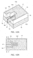
FIG. 3A to FIG. 7B . - As illustrated in
FIG. 3A , thefirst semiconductor layer 11 is grown on the major surface of asubstrate 10; and thelight emitting layer 12 and the second semiconductor layer 13are grown thereupon. In the case where such layers of thesemiconductor layer 15 are, for example, nitride semiconductors, thesemiconductor layer 15 may be formed by, for example, crystal growth on a sapphire substrate. - Then, as illustrated in
FIG. 3B , a separatingtrench 9 is made to pierce thesemiconductor layer 15 and reach thesubstrate 10 by, for example, Reactive Ion Etching (RIE) using a not-illustrated resist as a mask. The separatingtrench 9 is made, for example, in a lattice configuration on thesubstrate 10 to multiply separate thesemiconductor layer 15. - Then, a portion of the
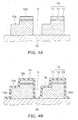
second semiconductor layer 13 and a portion of thelight emitting layer 12 is removed by, for example, RIE using a not-illustrated resist to expose a portion of thefirst semiconductor layer 11 as illustrated inFIG. 4A . Thereby, theupper level portion 15b is formed on the second major surface side of thesemiconductor layer 15 and positioned relatively in the upper level as viewed from thesubstrate 10; and thelower level portion 15c is formed on the second major surface side of thesemiconductor layer 15 and positioned more in the lower level on thesubstrate 10 side than is theupper level portion 15b. Theupper level portion 15b includes thelight emitting layer 12; and thelower level portion 15c does not include thelight emitting layer 12. - Continuing as illustrated in
FIG. 4B , the insulatingfilm 16 made of a silicon oxide film or the like is formed on all exposed faces of thesubstrate 10 by, for example, chemical vapor deposition (CVD). The insulatingfilm 16 covers exposed surface of thesemiconductor layer 15 including theside face 15d and the second major surface of thesemiconductor layer 15. And the insulatingfilm 16 also is formed on the side face and the bottom face of the separatingtrench 9. - Then, an opening is selectively made in the insulating
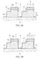
film 16 by, for example, wet etching to expose theside face 15d and the upper face (the second major surface) of thelower level portion 15c. Then, the n-side electrode 18 is formed as illustrated inFIG. 5A on the exposed portions by, for example, sputtering. At this time, the portions other than the portions where the n-side electrode 18 is formed are covered with a not-illustrated mask such as a resist. The n-side electrode 18 includes, for example, a nickel film formed on thefirst semiconductor layer 11 side and an aluminum film stacked on the nickel film. - Next, an opening is selectively made in the insulating
film 16 on theupper level portion 15b by, for example, wet etching to expose the upper face of theupper level portion 15b (the upper face of the second semiconductor layer 13). The p-side electrode 17 is formed as illustrated inFIG. 5B on the exposed portions by, for example, sputtering. At this time, the portions other than the portions where the p-side electrode 17 is formed are covered with a not-illustrated mask such as a resist. The p-side electrode 17 includes, for example, a nickel film formed on thesecond semiconductor layer 13 side and a gold film stacked on the nickel film. - The p-
side electrode 17 may be formed prior to the n-side electrode 18; or the p-side electrode 17 and the n-side electrode 18 may be formed simultaneously from the same material. - In case the metal utilized as the p-
side electrode 17 and the n-side electrode 18 are different, the manufacturing step is provided in two steps as inFIGS. 5A and 5B . However, in case the metal material is the same for the p-side electrode 17 and the n-side electrode 18, the manufacturing step may be one step. Namely, openings are formed in above a region to be formed the p-side electrode 17 and the n-side electrode 18 thereon. - Then, after covering the exposed portions of the
substrate 10 with the insulatinglayer 19, the insulatinglayer 19 is patterned as illustrated inFIG. 6A by, for example, wet etching to make thefirst opening 19a and thesecond opening 19b in the insulatinglayer 19. The insulatinglayer 19 is made of a resin such as, for example, polyimide having excellent patternability in ultra-fine patterns. - The
first opening 19a reaches the p-side electrode 17. Thesecond opening 19b reaches the n-side electrode 18 formed on the upper face of thelower level portion 15c. Further, thesecond opening 19b is made in the portion beside theside face 15d and communicates with the n-side electrode 18 formed on theside face 15d. - Then, a
continuous seed metal 20 is formed on the upper face of the insulatinglayer 19 and on the inner faces of thefirst opening 19a and thesecond opening 19b; and after forming a not-illustrated plating resist, Cu plating is performed using theseed metal 20 as a current path. Theseed metal 20 includes, for example, Cu. - Thereby, as illustrated in
FIG. 6B , the p-side interconnect layer 21 and the n-side interconnect layer 22 are formed selectively on the insulatinglayer 19. The p-side interconnect layer 21 and the n-side interconnect layer 22 are formed simultaneously by plating. The p-side interconnect layer 21 is formed also in thefirst opening 19a to connect to the p-side electrode 17. The n-side interconnect layer 22 is formed also in thesecond opening 19b to connect to the n-side electrode 18. - The
side face 15d is obtained when making the separatingtrench 9 described above referring toFIG. 3B . The separatingtrench 9 is made by RIE using a resist film selectively formed on thesemiconductor layer 15 as a mask. At this time, the resist film is consumed isotropically in the film thickness direction and the planar direction; and the planar size of the resist film is reduced as the etching progresses. Accordingly, the width of the separatingtrench 9 gradually decreases in the depth direction. Accordingly, each of the cross-sectional configurations of the multiply subdividedsemiconductor layer 15 on thesubstrate 10 is a trapezoidal configuration; and theside face 15d adjacent to the separatingtrench 9 is tapered with respect to the firstmajor surface 15a and the second major surface. - Therefore, the width of the portion of the
second opening 19b beside theside face 15d is wider upward; and it is possible to reliably form theseed metal 20 and the n-side interconnect layer 22 to the bottom of thesecond opening 19b. - The plating resist used during the plating of the p-
side interconnect layer 21 and the n-side interconnect layer 22 is removed by a chemical solution. Subsequently, another plating resist (not illustrated) is formed for forming the metal pillars; and Cu plating is performed using theseed metal 20 described above as a current path. Thereby, as illustrated inFIG. 7A , the p-side metal pillar 24 is formed above the p-side interconnect layer 21; and the n-side metal pillar 25 is formed above the n-side interconnect layer 22. The p-side metal pillar 24 and the n-side metal pillar 25 are formed simultaneously by plating. - Subsequently, the plating resist for forming the metal pillars is removed by a chemical solution; and the exposed portions of the
seed metal 20 also are removed. Thereby, the electrical connection between the p-side interconnect layer 21 and the n-side interconnect layer 22 via theseed metal 20 is divided. - Then, the p-
side interconnect layer 21, the n-side interconnect layer 22, the p-side metal pillar 24, and the n-side metal pillar 25 are covered with theresin layer 23. Subsequently, the surface of theresin layer 23 is polished to expose the end faces (the upper faces) of the p-side metal pillar 24 and the n-side metal pillar 25. - Subsequently, the
substrate 10 is removed. Thesubstrate 10 may be removed by, for example, laser lift-off. Specifically, laser light is irradiated from the backside of thesubstrate 10 toward thefirst semiconductor layer 11. Thesubstrate 10 is permeable to laser light; and the laser light has a wavelength in the absorption region of thefirst semiconductor layer 11. - When the laser light reaches the interface between the
substrate 10 and thefirst semiconductor layer 11, thefirst semiconductor layer 11 proximal to the interface absorbs the energy of the laser light and decomposes. For example, in the case where thefirst semiconductor layer 11 is GaN, thefirst semiconductor layer 11 decomposes into Ga and nitrogen gas. A micro gap is formed between thesubstrate 10 and thefirst semiconductor layer 11 by the decomposition reaction; and thesubstrate 10 and thefirst semiconductor layer 11 separate. The irradiation of the laser light is performed over the entire wafer by performing multiply for each set region; and thesubstrate 10 is removed. - Here, the layer made of the resin and the metal is flexible, and the metal is formed by plating at near room temperature. Hence, the residual stress occurring with respect to the
translucent substrate 10 is relatively low. - In the conventional technique for separating the semiconductor layer from the translucent substrate at wafer level, for example, it is bonded to a silicon substrate with a metal layer formed thereon using Au-Sn solder at a high temperature of 300 °C or more, and then the semiconductor layer made of GaN is separated by laser irradiation. However, in this conventional technique, the translucent substrate and the silicon substrate being different in thermal expansion coefficient are both rigid, and are bonded together at high temperature. Hence, a high residual stress remains between these substrates. Consequently, when the separation is started by laser irradiation, the residual stress is locally relieved from the separated portion and unfortunately causes cracks in the thin, brittle semiconductor layer.
- In contrast, in this embodiment, the residual stress is low, and the
semiconductor layer 15 is separated in the state of being fixed to a flexible support. Hence, the device can be manufactured at high yield without trouble such as cracking in thesemiconductor layer 15. - After removing the
substrate 10, thefluorescent layer 26 is formed on the firstmajor surface 15a as illustrated inFIG. 7B , Thefluorescent layer 26 may be formed, for example, by coating a liquid resin in which phosphor particles are mixed by spin coating and then thermosetting. - By forming the
fluorescent layer 26 after removing thesubstrate 10 from the firstmajor surface 15a, thesubstrate 10 does not exist between the firstmajor surface 15a and thefluorescent layer 26; and the light extraction efficiency can be increased. - Subsequently, dicing is performed to obtain the singulated semiconductor light emitting device illustrated in
FIG. 1A . During the dicing, thesubstrate 10 is already removed; and in the separatingtrench 9 which is the dicing region, thesemiconductor layer 15 does not exist and the insulatinglayer 19 which is a resin is filled. Accordingly, the dicing is easy because the insulatinglayer 19, which is a resin, and theresin layer 23 are cut; and the productivity can be improved. Further, damage to thesemiconductor layer 15 during the dicing can be avoided. Also, a structure is obtained after singulation in which the periphery of the device is covered with resin and protected. - The singulated semiconductor light emitting device may have a single-chip structure including one
semiconductor layer 15 or a multi-chip structure including multiple semiconductor layers 15. - Because the processes described above up to the dicing are performed collectively in the wafer state, it is unnecessary to perform interconnections and packaging for each of the singulated devices; and it is possible to drastically reduce production costs. The interconnections and the packaging are already complete in the singulated state. Moreover, downsizing is easy in the case where the planar size of each device approaches the planar size of the bare chip (the semiconductor layer 15). Also, inspections are possible at the wafer level. Therefore, the productivity can be increased. As a result, cost reductions are easy.
-
FIG. 8A is a schematic cross-sectional view of a semiconductor light emitting device of a second embodiment.FIG. 8B is a schematic perspective view of thesemiconductor layer 15 and theelectrodes FIG. 8A , the firstmajor surface 15a of thesemiconductor layer 15 is illustrated on the upper side; and inFIG. 8B , the firstmajor surface 15a is illustrated on the lower side. -
FIG. 9 illustrates one example of a planar layout of the semiconductor layer 15 (shown as broken line inFIG. 9 ), the p-side electrode 17 (shown as broken line inFIG. 9 ), the p-side interconnect layer 21, the n-side interconnect layer 22, the p-side metal pillar 24, and the n-side metal pillar 25 of this embodiment.FIG. 9 corresponds to a plan view as viewed from the lower face (the mounting surface) side ofFIG. 8A . Theresin layer 23 is not illustrated. - In this embodiment as well, the n-
side electrode 18 is formed on theside face 15d of thefirst semiconductor layer 11 between the firstmajor surface 15a and thelight emitting layer 12 of thesemiconductor layer 15. Thereby, the surface area reduction of the p-side electrode 17 can be suppressed; the luminance can be increased; and the reliability can be increased by increasing the surface area of the n-side electrode 18. Further, the light leakage from theside face 15d can be prevented; and the uneven colors and the uneven luminance can be suppressed. Also, the amount of light reflected by the side face and extracted from the firstmajor surface 15a side can be increased; and the luminance can be increased. - In this embodiment, the n-
side electrode 18 is not provided on the second major surface and is provided only on theside face 15d. Accordingly, as illustrated inFIG. 8B andFIG. 9 , the surface area of the p-side electrode 17 provided on the second major surface can be greater; and a larger light emitting region can be obtained. Thereby, the luminous efficacy can be increased. Because the processes described above and illustrated inFIG. 4A that expose the second major surface of thefirst semiconductor layer 11 can be omitted, cost reductions also are possible. -
FIG. 10A is a schematic perspective view of thesemiconductor layer 15 and theelectrodes -
FIG. 10B corresponds to a plan view ofFIG. 10A . -
FIG. 11A corresponds to a cross section along A-A ofFIG. 10B . -
FIG. 11B corresponds to a cross section along B-B ofFIG. 11A . -
FIG. 12 illustrates one example of a planar layout of thesemiconductor layer 15, the p-side electrode 17, the n-side electrode 18, the p-side interconnect layer 21, the n-side interconnect layer 22, the p-side metal pillar 24, and the n-side metal pillar 25 of this embodiment.FIG. 12 corresponds to a plan view as viewed from the lower face (the mounting surface) side ofFIG. 11B . Theresin layer 23 is not illustrated. - On the second major surface of the
semiconductor layer 15, the layout of the p-side electrode 17 has a surface area greater than that of the n-side electrode 18. The n-side interconnect layer 22 is formed to spread over the insulatinglayer 19 with a surface area greater than that of the portion of the n-side electrode 18 provided on the second major surface. - In this embodiment as well, the n-
side electrode 18 is formed on theside face 15d and the upper face (the second major surface) of thelower level portion 15c of thesemiconductor layer 15. In this embodiment, atrench 41 is formed in thelower level portion 15c. Thetrench 41 is formed from the second major surface of thelower level portion 15c to reach thesubstrate 10 in a state in which thesemiconductor layer 15 is formed on thesubstrate 10. In other words, thetrench 41 reaches the firstmajor surface 15a from the second major surface of thelower level portion 15c. Thetrench 41 pierces the n-type semiconductor layer 11. The n-side electrode 18 is formed also on the side face of thetrench 41. - In addition to the
side face 15d which is the outer circumferential face of thelower level portion 15c, the n-side electrode 18 is formed also on the side face of thetrench 41. Thereby, the region of the n-side electrode 18 on the second major surface can be reduced. The surface area of the p-side electrode 17 on the second major surface can be relatively increased; and the luminous efficacy can be increased. - In this embodiment, the
semiconductor layer 15 has arecess portion 15r toward longitudinal direction. Therecess portion 15r is set back one move step with comparing to the semiconductor light emitting device shown inFIGS. 1A, 1B and2 . Further, thesemiconductor layer 15 is two step recesses, in which one is wide and provided outside and theother recess portion 15r is narrow, as shown inFIGS. 10A and 10B . In therecess portion 15r, a protrudedportion 182 of the n-side electrode 18 is formed. As shown inFIG. 10B , the n-side electrode 18 has aprotrusion portion 182 toward the p-side electrode 17 in longitudinal direction (horizontal direction inFIG. 10B ) of the semiconductor light emitting device. - The n-
side electrode 18 includes awide portion 181 and a narrow (protruded)portion 182. Thewide portion 181 is similar to the n-side electrode 18 inFIGS. 1A, 1B and2 . - The
trench 41 is formed from thelower level portion 15c and therecess portion 15r to the firstmajor surface 15a. Thetrench 41 has a line shape in a plan view inFIG. 10B , and uniform width, in this embodiment. Theprotrusion portion 182 is protruded a bottom of the U shape of the p-side electrode 17 as inFIGS. 10B and12 . - In this embodiment as well, the light leakage from the
side face 15d can be prevented; and the uneven colors and the uneven luminance can be suppressed. Further, the amount of the light reflected by the side face and extracted from the firstmajor surface 15a side can be increased; and the luminance can be increased. - As illustrated in
FIG. 11A , the n-side electrode 18 is formed also on the bottom portion of thetrench 41. The n-side electrode 18 is formed on the bottom portion of thetrench 41, i.e., the major surface of thesubstrate 10, in the state in which thesemiconductor layer 15 is formed on thesubstrate 10. Therefore, thefluorescent layer 26 does not enter thetrench 41 when forming thefluorescent layer 26 on the firstmajor surface 15a after removing thesubstrate 10; and thefluorescent layer 26 can be formed with a uniform thickness. - The n-
side interconnect layer 22 is filled also on the inner side of the n-side electrode 18 in thetrench 41. Accordingly, the n-side electrode 18 and the n-side interconnect layer 22 are in contact also inside thetrench 41. Therefore, the contact surface area between the n-side electrode 18 and the n-side interconnect layer 22 can be increased; and the contact resistance can be reduced. - The
trench 41 is made from the second major surface of thelower level portion 15c to reach the firstmajor surface 15a on the side opposite to the second major surface. Thesubstrate 10 forms a stopper when patterning thetrench 41; and thetrench 41 can be obtained with a constant depth. Therefore, characteristic variations due to variation of the contact surface area between the n-side electrode 18 and thefirst semiconductor layer 11 via the side face of thetrench 41 can be prevented. - As shown in
FIG. 12 , the n-side metal pillar 25 is provided above (beneath) thewide portion 181 and the narrow protrudedportion 182 of the n-side electrode 18. - In this embodiment, the narrow protruded
portion 182 of the n-side electrode 18 is provided. Therefore, a radiative recombination is generated around a center of the semiconductor light emitting device. Furthermore, thetrench 41 is formed and the n-side electrode 18 is formed on the side surface of thetrench 41. Thus, a current pass from the p-side electrode 17 to the n-side electrode 18 is spread and optical output may be improved. -
FIG. 13A is a schematic cross-sectional view of a semiconductor light emitting device of an illustrative example.FIG. 13B is a schematic perspective view of thesemiconductor layer 15 and theelectrodes -
FIG. 14 illustrates one example of a planar layout of thesemiconductor layer 15, the p-side electrode 17, the n-side electrode 18, the p-side interconnect layer 21, the n-side interconnect layer 22, the p-side metal pillar 24, and the n-side metal pillar 25 of this illustrative example.FIG. 14 corresponds to a plan view as viewed from the lower face (the mounting surface) ofFIG. 13A . Theresin layer 23 is not illustrated. - The layout of the p-
side electrode 17 on the second major surface of thesemiconductor layer 15 has a surface area greater than that of the n-side electrode 18. The n-side interconnect layer 22 is formed to spread over the insulatinglayer 19 with a surface area greater than that of the n-side electrode 18 provided on the second major surface. - The p-
side electrode 17 is provided on the second major surface of theupper level portion 15b including thelight emitting layer 12; and the n-side electrode 18 is provided on the second major surface of thelower level portion 15c provided outside the outer circumference of thelight emitting layer 12. - In this illustrative example, the p-
side electrode 17 is provided also on theside face 15d side of thesemiconductor layer 15. The insulatingfilm 16 is formed on theside face 15d; and the p-side electrode 17 is provided also on the insulatingfilm 16 provided on theside face 15d. - The p-
side electrode 17 is provided via the insulatingfilm 16 on theside face 15d on the side opposite to thelower level portion 15c with theupper level portion 15b between theside face 15d and thelower level portion 15c. The p-side electrode 17 is formed continuously from the second major surface of theupper level portion 15b to theside face 15d side. - A high potential (a positive potential) with respect to the n-
side electrode 18 may be applied to the p-side electrode 17. Then, electrons injected from the n-side electrode 18 into thefirst semiconductor layer 11 are attracted by the potential of the p-side electrode 17 provided on theside face 15d side; and the electrons can be efficiently injected even into the portions of thelight emitting layer 12 distal to the n-side electrode 18 as illustrated by the broken-line arrows ofFIG. 13A . - Accordingly, the concentration of the electrons in the side of the
light emitting layer 12 proximal to the n-side electrode 18 can be suppressed; the current distribution in the surface direction of thelight emitting layer 12 can be uniform; and a local increase of the current density can be suppressed. In other words, the electrons contribute more efficiently to the light emission; and the luminous efficacy increases. - Although the n-
side electrode 18 is provided only on the second major surface in the structure illustrated inFIGS. 13A and 13B , the n-side electrode 18 may be formed on the side face of thelower level portion 15c similarly to the embodiments described above. In such a case, the p-side electrode 17 and the n-side electrode 18 are separated from each other by an insulating film such that theelectrodes side face 15d. - In the embodiments described above, the
substrate 10 may not be removed entirely; and thesubstrate 10 may be polished to thinly remain on the firstmajor surface 15a. By leaving thesubstrate 10 in a thin layer, the mechanical strength can be higher than that of the structure in which thesubstrate 10 is entirely removed; and a structure having high reliability can be provided. The remainingsubstrate 10 can suppress warp after singulation; and the mounting onto the circuit substrate and the like is easy. - A red fluorescent layer may contain, for example, a nitride-based phosphor of CaAlSiN3:Eu or a SiAlON-based phosphor.
- In the case where a SiAlON-based phosphor is used, it may be used

where M is at least one type of metal element excluding Si and Al, and it may be desirable for M to be at least one selected from Ca and Sr; R is a light emission center element, and it may be desirable for R to be Eu; and x, a1, b1, c1, and d1 satisfy the relationships 0 < x ≤ 1, 0.6 < a1 < 0.95, 2 < b1 < 3.9, 0.25 < c1 < 0.45, and 4 < d1 < 5.7. - By using the SiAlON-based phosphor of Compositional Formula (1), the temperature characteristics of the wavelength conversion efficiency can be improved; and the efficiency in the high current density region can be improved further.
- A yellow fluorescent layer may contain, for example, a silicate-based phosphor of (Sr, Ca, Ba)2SiO4: Eu.
- A green fluorescent layer may contain, for example, a halophosphate-based phosphor of (Ba, Ca, Mg)10(PO4)6·Cl2:Eu or a SiAlON-based phosphor.
- In the case where a SiAlON-based phosphor is used, it may be used

where M is at least one type of metal element excluding Si and Al, and it may be desirable for M to be at least one selected from Ca and Sr; R is a light emission center element, and it may be desirable for R to be Eu; and x, a2, b2, c2, and d2 satisfy the relationships 0 < x ≤ 1, 0.93 < a2 < 1.3, 4.0 < b2 <5.8, 0.6 < c2 <1, and 6 < d2 < 11. - By using the SiAlON-based phosphor of Compositional Formula (2), the temperature characteristics of the wavelength conversion efficiency can be improved; and the efficiency in the high current density region can be improved further.
- A blue fluorescent layer may contain, for example, an oxide-based phosphor of BaMgAl10O17:Eu.
- According to this embodiment, the method for manufacturing the semiconductor light emitting device includes:
- forming a semiconductor layer on a substrate, the semiconductor layer including a light emitting layer, a first major surface, and a second major surface formed on a side opposite to the first major surface;
- making a separating trench on the substrate to multiply separate the semiconductor layer;
- forming a first electrode on the second major surface of the semiconductor layer;
- forming a second electrode on a side face adjacent to the separating trench, the side face being a portion between the first major surface and the light emitting layer of the semiconductor layer;
- forming a first insulating layer to cover the first electrode and the second electrode on the second major surface side of the semiconductor layer;
- making a first opening in the first insulating layer to reach the first electrode and making a second opening in the first insulating layer to reach the second electrode provided on the side face;
- forming a first interconnect layer in the first opening and on the first insulating layer on a side opposite to the second major surface;
- forming a second interconnect layer in the second opening and on the first insulating layer on the side opposite to the second major surface;
- forming the first metal pillar on a face of the first interconnect layer on a side opposite to the first electrode;
- forming a second metal pillar on a face of the second interconnect layer on a side opposite to the second electrode; and
- forming a second insulating layer to cover a periphery of the first metal pillar and a periphery of the second metal pillar.
- The manufacturing method further includes forming an upper level portion including the light emitting layer and a lower level portion not including the light emitting layer on the second major surface side of the semiconductor layer.
- The second electrode is formed on a side face of the lower level portion.
- The second electrode is formed also on an upper face of the lower level portion.
- The manufacturing method further includes making a trench to pierce the lower level portion and reach the substrate; and the second electrode is formed also on a side face of the trench.
- A resin is filled as an insulating layer into the separating trench; and singulation is performed by cutting the resin in the separating trench.
- While certain embodiments have been described, these embodiments have been presented by way of example only, and are not intended to limit the scope of the inventions. Indeed, the novel embodiments described herein may be embodied in a variety of other forms; furthermore, various omissions, substitutions and changes in the form of the embodiments described herein may be made. The accompanying claims define the scope invention.
Claims (17)
- A semiconductor light emitting device, comprising:a semiconductor layer (15) including a light emitting layer (12), the semiconductor layer (15) having a first major surface (15a), and a second major surface opposite to the first major surface (15a);a first electrode (17) provided on the second major surface of the semiconductor layer (15);a second electrode (18) provided on a side face (15d) of a portion of the semiconductor layer (15) between the light emitting layer (12) and the first major surface (15a);a first insulating layer (19) provided on a side of the second major surface of the semiconductor layer (15), the first insulating layer (19) having a first opening (19a) reaching the first electrode (17);a first interconnect layer (21) provided in the first opening (19a) and on the first insulating layer (19) on a side of the first insulating layer (19) opposite to the second major surface to connect to the first electrode (17); anda second interconnect layer (22);characterized in thatthe first insulating layer (19) has a second opening (19b) provided on the side face (15d) reaching the second electrode (18);the second interconnect layer (22) is provided in the second opening (19b) and on the first insulating layer (19) on the side of the first insulating layer (19) opposite to the second major surface to connect to the second electrode (18) provided on the side face (15d), the second interconnect layer (22) provided on the side face (15d) of the portion of the semiconductor layer (15) with interposing the second electrode (18); andfurther comprisinga first metal pillar (24) provided on a face of the first interconnect layer (21) on a side opposite to the first electrode (17);a second metal pillar (25) provided on a face of the second interconnect layer (22) on a side opposite to the second electrode (18); anda second insulating layer (23) covering a periphery of the first metal pillar (24) and a periphery of the second metal pillar (25).
- The device of claim 1, wherein the second electrode (18) is provided to continuously enclose the side face (15d).
- The device of claim 1 or 2, wherein the second electrode (18) is provided also on the second major surface.
- The device of claim 3, wherein a surface area of the second electrode (18) on the side face (15d) is greater than a surface area of the second electrode (18) on the second major surface.
- The device of claim 3 or 4, wherein the first electrode (17) has a U shape in a plan view, and a portion of the second electrode (18) is provided in an opening of the U shape in a plan view.
- The device of claim 5, wherein the second electrode (18) has a protrusion portion on the second major surface toward a bottom of the U shape in a plan view.
- The device of any of claims 1-6, wherein the semiconductor layer (15) includes an upper level portion (15b) including the light emitting layer (12) and a lower level portion (15c) not including the light emitting layer (12), the first electrode (17) is provided on the second major surface of the upper level portion (15b), and the second electrode (18) is provided on a side face of the lower level portion (15c).
- The device of claim 7, wherein
a trench (41) is formed in the lower level portion (15c), and
the second electrode (18) is provided also on a side face of the trench (41). - The device of claim 8, wherein the second electrode (18) is provided also on a bottom portion of the trench (41).
- The device of claim 8 or 9, wherein the second interconnect layer (22) is provided also on an inner side of the second electrode (18) in the trench (41).
- The device of any of claims 7-10, wherein the second electrode (18) is provided also on the second major surface of the lower level portion (15c).
- The device of claim 11, wherein the first electrode (17) has a U shape in a plan view, a portion of the second electrode (18) is provided in an opening of the U shape in a plan view, and the second electrode (18) has a protrusion portion (182) on the second major surface toward a bottom of the U shape in a plan view.
- The device of claim 12, wherein a trench (41) is formed in the lower level portion (15c) and the protrusion portion (182), and the second electrode (18) is provided also on a side face of the trench (41).
- The device of any of claims 1-13, wherein
the side face (15d) is tapered with respect to the first major surface (15a) and the second major surface, and
a width of a portion of the second opening (19b) beside the side face (15d) gradually increases from a side of the first major surface (15a) toward a side of the second major surface. - The device of any of claims 3-14, wherein a face of the second interconnect layer (22) on a side opposite to the second electrode (18) on the second major surface is larger than a face of the second interconnect layer (22) connected to the second electrode (18) on the second major surface.
- The device of any of claims 3-15, wherein a surface area of a portion of the second electrode (18) provided on the side face (15d) of the semiconductor layer (15) is greater than a surface area of a portion of the second electrode (18) provided on the second major surface.
- The device of any of claims 1-16, wherein each of a thickness of the first metal pillar (24) and a thickness of the second metal pillar (25) is thicker than a thickness of a stacked body including the semiconductor layer (15), the first electrode (17), the second electrode (18), the first insulating layer (19), the first interconnect layer (21), and the second interconnect layer (22).
Applications Claiming Priority (1)
| Application Number | Priority Date | Filing Date | Title |
|---|---|---|---|
| JP2010118697A JP5356312B2 (en) | 2010-05-24 | 2010-05-24 | Semiconductor light emitting device |
Publications (2)
| Publication Number | Publication Date |
|---|---|
| EP2390933A1 EP2390933A1 (en) | 2011-11-30 |
| EP2390933B1 true EP2390933B1 (en) | 2015-05-20 |
Family
ID=44019032
Family Applications (1)
| Application Number | Title | Priority Date | Filing Date |
|---|---|---|---|
| EP20100186525 Not-in-force EP2390933B1 (en) | 2010-05-24 | 2010-10-05 | Semiconductor light emitting device |
Country Status (5)
| Country | Link |
|---|---|
| US (1) | US8729592B2 (en) |
| EP (1) | EP2390933B1 (en) |
| JP (1) | JP5356312B2 (en) |
| HK (1) | HK1163348A1 (en) |
| TW (1) | TWI445207B (en) |
Families Citing this family (41)
| Publication number | Priority date | Publication date | Assignee | Title |
|---|---|---|---|---|
| CN102792471A (en) * | 2010-04-01 | 2012-11-21 | 松下电器产业株式会社 | Light-emitting diode element and light-emitting diode device |
| JP5343040B2 (en) * | 2010-06-07 | 2013-11-13 | 株式会社東芝 | Semiconductor light emitting device |
| JP5537446B2 (en) | 2011-01-14 | 2014-07-02 | 株式会社東芝 | Light emitting device, light emitting module, and method of manufacturing light emitting device |
| JP5603793B2 (en) | 2011-02-09 | 2014-10-08 | 株式会社東芝 | Semiconductor light emitting device |
| JP5603813B2 (en) | 2011-03-15 | 2014-10-08 | 株式会社東芝 | Semiconductor light emitting device and light emitting device |
| JP5535114B2 (en) | 2011-03-25 | 2014-07-02 | 株式会社東芝 | Light emitting device, light emitting module, and method of manufacturing light emitting device |
| JP5642623B2 (en) | 2011-05-17 | 2014-12-17 | 株式会社東芝 | Semiconductor light emitting device |
| RU2597071C2 (en) | 2011-05-24 | 2016-09-10 | Конинклейке Филипс Н.В. | METAL FILLER, SEPARATING p- AND n-TYPE LAYERS, FOR LIGHT-EMITTING DIODES MOUNTED BY FLIP-CHIP METHOD |
| JP5662277B2 (en) | 2011-08-08 | 2015-01-28 | 株式会社東芝 | Semiconductor light emitting device and light emitting module |
| JP2013065726A (en) | 2011-09-16 | 2013-04-11 | Toshiba Corp | Semiconductor light-emitting device and method of manufacturing the same |
| KR102012292B1 (en) * | 2011-12-08 | 2019-08-20 | 루미리즈 홀딩 비.브이. | Semiconductor light emitting device with thick metal layers |
| US20130240934A1 (en) * | 2012-03-14 | 2013-09-19 | Samsung Electronics Co., Ltd. | Light emitting element package and method of manufacturing the same |
| JP5985322B2 (en) | 2012-03-23 | 2016-09-06 | 株式会社東芝 | Semiconductor light emitting device and manufacturing method thereof |
| JP5710532B2 (en) * | 2012-03-26 | 2015-04-30 | 株式会社東芝 | Semiconductor light emitting device and manufacturing method thereof |
| CN102646769B (en) * | 2012-03-30 | 2015-08-05 | 达亮电子(苏州)有限公司 | Light-emitting diode component, package structure for LED and manufacture method thereof |
| WO2013171632A1 (en) * | 2012-05-17 | 2013-11-21 | Koninklijke Philips N.V. | Method of separating a wafer of semiconductor devices |
| FR2992465B1 (en) * | 2012-06-22 | 2015-03-20 | Soitec Silicon On Insulator | METHOD FOR THE COLLECTIVE PRODUCTION OF LEDS AND STRUCTURE FOR THE COLLECTIVE MANUFACTURE OF LEDS |
| FR2992466A1 (en) * | 2012-06-22 | 2013-12-27 | Soitec Silicon On Insulator | Method for manufacturing e.g. LED device, involves forming insulating material portion on sides of p-type layer, active layer and portion of n-type layer, and exposing contact studs over another portion of n-type layer |
| US8816383B2 (en) * | 2012-07-06 | 2014-08-26 | Invensas Corporation | High performance light emitting diode with vias |
| JP6239311B2 (en) * | 2012-08-20 | 2017-11-29 | エルジー イノテック カンパニー リミテッド | Light emitting element |
| KR101886156B1 (en) * | 2012-08-21 | 2018-09-11 | 엘지이노텍 주식회사 | Light emitting device |
| DE102012113003A1 (en) * | 2012-12-21 | 2014-04-03 | Osram Opto Semiconductors Gmbh | Method for producing an optoelectronic semiconductor component and optoelectronic semiconductor component |
| JP2015050256A (en) * | 2013-08-30 | 2015-03-16 | 株式会社東芝 | Nitride semiconductor light-emitting device |
| FR3023065B1 (en) * | 2014-06-27 | 2017-12-15 | Commissariat Energie Atomique | P-N JUNCTION OPTOELECTRONIC DEVICE FOR IONIZATION OF FIELD EFFECT DOPANTS |
| FR3023061B1 (en) * | 2014-06-27 | 2017-12-15 | Commissariat Energie Atomique | MESA STRUCTURE DIODE WITH SUBSTANTIALLY PLANE CONTACT SURFACE |
| CN105449064B (en) * | 2014-09-02 | 2018-02-23 | 展晶科技(深圳)有限公司 | Light emitting diode and its manufacture method |
| KR102322841B1 (en) * | 2014-12-24 | 2021-11-08 | 엘지이노텍 주식회사 | Light emittng device and light emitting device array including the same |
| KR102322842B1 (en) * | 2014-12-26 | 2021-11-08 | 엘지이노텍 주식회사 | Light emitting device array |
| KR102345751B1 (en) | 2015-01-05 | 2022-01-03 | 삼성전자주식회사 | Semiconductor light emitting device package and method for manufacturing the same |
| JP6545981B2 (en) | 2015-03-12 | 2019-07-17 | アルパッド株式会社 | Semiconductor light emitting device |
| DE102015107586B4 (en) | 2015-05-13 | 2023-10-26 | OSRAM Opto Semiconductors Gesellschaft mit beschränkter Haftung | Method for producing optoelectronic components and surface-mountable optoelectronic component |
| FR3038127B1 (en) * | 2015-06-24 | 2017-06-23 | Commissariat Energie Atomique | METHOD FOR MANUFACTURING A PLURALITY OF ISLET-SHAPED DIPOLES HAVING SELF-ALIGNED ELECTRODES |
| US11387392B2 (en) * | 2018-12-25 | 2022-07-12 | Nichia Corporation | Light-emitting device and display device |
| JP7348520B2 (en) | 2018-12-25 | 2023-09-21 | 日亜化学工業株式会社 | Light emitting device and display device |
| JP7052188B2 (en) * | 2019-06-13 | 2022-04-12 | 日亜化学工業株式会社 | Manufacturing method of light emitting element |
| CN112582511B (en) * | 2019-09-30 | 2022-08-02 | 成都辰显光电有限公司 | Micro light emitting diode chip and display panel |
| CN112768484B (en) * | 2019-11-04 | 2024-03-26 | 厦门三安光电有限公司 | Light emitting diode and manufacturing method thereof |
| CN112968089B (en) * | 2020-11-26 | 2022-04-15 | 重庆康佳光电技术研究院有限公司 | Light emitting device and manufacturing method thereof, and back plate and manufacturing method thereof |
| US11955583B2 (en) * | 2020-12-01 | 2024-04-09 | Lumileds Llc | Flip chip micro light emitting diodes |
| US11705534B2 (en) * | 2020-12-01 | 2023-07-18 | Lumileds Llc | Methods of making flip chip micro light emitting diodes |
| CN115249757A (en) * | 2022-09-20 | 2022-10-28 | 南昌凯捷半导体科技有限公司 | Step-free mini LED chip and manufacturing method thereof |
Citations (1)
| Publication number | Priority date | Publication date | Assignee | Title |
|---|---|---|---|---|
| US20020017651A1 (en) * | 2000-07-25 | 2002-02-14 | Munehiro Kato | White light emission diode |
Family Cites Families (25)
| Publication number | Priority date | Publication date | Assignee | Title |
|---|---|---|---|---|
| JP2661420B2 (en) | 1991-07-16 | 1997-10-08 | 豊田合成株式会社 | Method of manufacturing gallium nitride based compound semiconductor light emitting device |
| JP3557033B2 (en) * | 1995-03-24 | 2004-08-25 | 三洋電機株式会社 | Semiconductor light emitting device and method of manufacturing the same |
| US5798536A (en) * | 1996-01-25 | 1998-08-25 | Rohm Co., Ltd. | Light-emitting semiconductor device and method for manufacturing the same |
| JP3556080B2 (en) * | 1997-11-14 | 2004-08-18 | 日亜化学工業株式会社 | Nitride semiconductor device |
| JP2000150958A (en) | 1998-11-13 | 2000-05-30 | Sanyo Electric Co Ltd | Semiconductor light emitting device |
| JP3589187B2 (en) * | 2000-07-31 | 2004-11-17 | 日亜化学工業株式会社 | Method for forming light emitting device |
| JP4644947B2 (en) * | 2001-02-05 | 2011-03-09 | 日亜化学工業株式会社 | Nitride semiconductor device and manufacturing method thereof |
| JP2002353503A (en) * | 2001-05-29 | 2002-12-06 | Seiwa Electric Mfg Co Ltd | Gallium-nitride based compound semiconductor light- emitting element |
| JP4214704B2 (en) * | 2002-03-20 | 2009-01-28 | 日亜化学工業株式会社 | Semiconductor element |
| CN100595938C (en) * | 2002-08-01 | 2010-03-24 | 日亚化学工业株式会社 | Semiconductor light emitting device, manufacturing method thereof, and light emitting device using the same |
| US7179670B2 (en) * | 2004-03-05 | 2007-02-20 | Gelcore, Llc | Flip-chip light emitting diode device without sub-mount |
| TWI244228B (en) * | 2005-02-03 | 2005-11-21 | United Epitaxy Co Ltd | Light emitting device and manufacture method thereof |
| KR100616693B1 (en) | 2005-08-09 | 2006-08-28 | 삼성전기주식회사 | Semiconductor light emitting device |
| JP2007288097A (en) * | 2006-04-20 | 2007-11-01 | Showa Denko Kk | Printed-circuit board and mounting structure of flip-chip semiconductor light-emitting device, and light-emitting diode lamp |
| JP2007184316A (en) * | 2006-01-04 | 2007-07-19 | Toshiba Corp | Semiconductor device |
| KR20070111091A (en) | 2006-05-16 | 2007-11-21 | 삼성전기주식회사 | Nitride semiconductor light emitting diode |
| WO2008026902A1 (en) | 2006-08-31 | 2008-03-06 | Epivalley Co., Ltd. | Iii-nitride semiconductor light emitting device |
| WO2008031280A1 (en) | 2006-09-13 | 2008-03-20 | Helio Optoelectronics Corporation | Light emitting diode structure |
| DE102007019776A1 (en) | 2007-04-26 | 2008-10-30 | Osram Opto Semiconductors Gmbh | Optoelectronic component and method for producing a plurality of optoelectronic components |
| US8368100B2 (en) * | 2007-11-14 | 2013-02-05 | Cree, Inc. | Semiconductor light emitting diodes having reflective structures and methods of fabricating same |
| US9634191B2 (en) * | 2007-11-14 | 2017-04-25 | Cree, Inc. | Wire bond free wafer level LED |
| US8431950B2 (en) | 2008-05-23 | 2013-04-30 | Chia-Lun Tsai | Light emitting device package structure and fabricating method thereof |
| JP5286045B2 (en) * | 2008-11-19 | 2013-09-11 | スタンレー電気株式会社 | Manufacturing method of semiconductor light emitting device |
| JP4724222B2 (en) | 2008-12-12 | 2011-07-13 | 株式会社東芝 | Method for manufacturing light emitting device |
| JP5197654B2 (en) * | 2010-03-09 | 2013-05-15 | 株式会社東芝 | Semiconductor light emitting device and manufacturing method thereof |
-
2010
- 2010-05-24 JP JP2010118697A patent/JP5356312B2/en not_active Expired - Fee Related
- 2010-09-08 TW TW099130334A patent/TWI445207B/en not_active IP Right Cessation
- 2010-09-20 US US12/886,092 patent/US8729592B2/en not_active Expired - Fee Related
- 2010-10-05 EP EP20100186525 patent/EP2390933B1/en not_active Not-in-force
-
2012
- 2012-04-19 HK HK12103875.0A patent/HK1163348A1/en unknown
Patent Citations (1)
| Publication number | Priority date | Publication date | Assignee | Title |
|---|---|---|---|---|
| US20020017651A1 (en) * | 2000-07-25 | 2002-02-14 | Munehiro Kato | White light emission diode |
Also Published As
| Publication number | Publication date |
|---|---|
| US20110284910A1 (en) | 2011-11-24 |
| JP5356312B2 (en) | 2013-12-04 |
| EP2390933A1 (en) | 2011-11-30 |
| US8729592B2 (en) | 2014-05-20 |
| HK1163348A1 (en) | 2012-09-07 |
| TW201143141A (en) | 2011-12-01 |
| TWI445207B (en) | 2014-07-11 |
| JP2011249425A (en) | 2011-12-08 |
Similar Documents
| Publication | Publication Date | Title |
|---|---|---|
| EP2390933B1 (en) | Semiconductor light emitting device | |
| US9136437B2 (en) | Semiconductor light emitting device and method for manufacturing same | |
| US8692279B2 (en) | Semiconductor light emitting device | |
| EP2393131B1 (en) | Semiconductor light emitting device and method for manufacturing same | |
| EP2393135B1 (en) | Semiconductor light emitting device and method for manufacturing the same | |
| US8436378B2 (en) | Semiconductor light emitting device and method for manufacturing same | |
| US8378377B2 (en) | Light emitting device | |
| US8941124B2 (en) | Semiconductor light emitting device and method for manufacturing same | |
| US9263640B2 (en) | Semiconductor light emitting device | |
| EP2423988A1 (en) | Semiconductor light emitting device | |
| EP2325905A2 (en) | Semiconductor light-emitting device and method for manufacturing same | |
| US8174027B2 (en) | Semiconductor light emitting device and method for manufacturing same |
Legal Events
| Date | Code | Title | Description |
|---|---|---|---|
| 17P | Request for examination filed |
Effective date: 20101005 |
|
| AK | Designated contracting states |
Kind code of ref document: A1 Designated state(s): AL AT BE BG CH CY CZ DE DK EE ES FI FR GB GR HR HU IE IS IT LI LT LU LV MC MK MT NL NO PL PT RO RS SE SI SK SM TR |
|
| AX | Request for extension of the european patent |
Extension state: BA ME |
|
| PUAI | Public reference made under article 153(3) epc to a published international application that has entered the european phase |
Free format text: ORIGINAL CODE: 0009012 |
|
| REG | Reference to a national code |
Ref country code: HK Ref legal event code: DE Ref document number: 1163348 Country of ref document: HK |
|
| 17Q | First examination report despatched |
Effective date: 20120822 |
|
| GRAJ | Information related to disapproval of communication of intention to grant by the applicant or resumption of examination proceedings by the epo deleted |
Free format text: ORIGINAL CODE: EPIDOSDIGR1 |
|
| GRAP | Despatch of communication of intention to grant a patent |
Free format text: ORIGINAL CODE: EPIDOSNIGR1 |
|
| INTG | Intention to grant announced |
Effective date: 20141212 |
|
| GRAS | Grant fee paid |
Free format text: ORIGINAL CODE: EPIDOSNIGR3 |
|
| GRAA | (expected) grant |
Free format text: ORIGINAL CODE: 0009210 |
|
| AK | Designated contracting states |
Kind code of ref document: B1 Designated state(s): AL AT BE BG CH CY CZ DE DK EE ES FI FR GB GR HR HU IE IS IT LI LT LU LV MC MK MT NL NO PL PT RO RS SE SI SK SM TR |
|
| REG | Reference to a national code |
Ref country code: GB Ref legal event code: FG4D |
|
| REG | Reference to a national code |
Ref country code: CH Ref legal event code: EP |
|
| REG | Reference to a national code |
Ref country code: AT Ref legal event code: REF Ref document number: 728135 Country of ref document: AT Kind code of ref document: T Effective date: 20150615 |
|
| REG | Reference to a national code |
Ref country code: IE Ref legal event code: FG4D |
|
| REG | Reference to a national code |
Ref country code: DE Ref legal event code: R096 Ref document number: 602010024722 Country of ref document: DE |
|
| REG | Reference to a national code |
Ref country code: NL Ref legal event code: T3 |
|
| REG | Reference to a national code |
Ref country code: FR Ref legal event code: PLFP Year of fee payment: 6 |
|
| REG | Reference to a national code |
Ref country code: AT Ref legal event code: MK05 Ref document number: 728135 Country of ref document: AT Kind code of ref document: T Effective date: 20150520 |
|
| REG | Reference to a national code |
Ref country code: LT Ref legal event code: MG4D |
|
| PG25 | Lapsed in a contracting state [announced via postgrant information from national office to epo] |
Ref country code: ES Free format text: LAPSE BECAUSE OF FAILURE TO SUBMIT A TRANSLATION OF THE DESCRIPTION OR TO PAY THE FEE WITHIN THE PRESCRIBED TIME-LIMIT Effective date: 20150520 Ref country code: NO Free format text: LAPSE BECAUSE OF FAILURE TO SUBMIT A TRANSLATION OF THE DESCRIPTION OR TO PAY THE FEE WITHIN THE PRESCRIBED TIME-LIMIT Effective date: 20150820 Ref country code: LT Free format text: LAPSE BECAUSE OF FAILURE TO SUBMIT A TRANSLATION OF THE DESCRIPTION OR TO PAY THE FEE WITHIN THE PRESCRIBED TIME-LIMIT Effective date: 20150520 Ref country code: FI Free format text: LAPSE BECAUSE OF FAILURE TO SUBMIT A TRANSLATION OF THE DESCRIPTION OR TO PAY THE FEE WITHIN THE PRESCRIBED TIME-LIMIT Effective date: 20150520 Ref country code: HR Free format text: LAPSE BECAUSE OF FAILURE TO SUBMIT A TRANSLATION OF THE DESCRIPTION OR TO PAY THE FEE WITHIN THE PRESCRIBED TIME-LIMIT Effective date: 20150520 Ref country code: PT Free format text: LAPSE BECAUSE OF FAILURE TO SUBMIT A TRANSLATION OF THE DESCRIPTION OR TO PAY THE FEE WITHIN THE PRESCRIBED TIME-LIMIT Effective date: 20150921 |
|
| PGFP | Annual fee paid to national office [announced via postgrant information from national office to epo] |
Ref country code: GB Payment date: 20150930 Year of fee payment: 6 |
|
| PG25 | Lapsed in a contracting state [announced via postgrant information from national office to epo] |
Ref country code: LV Free format text: LAPSE BECAUSE OF FAILURE TO SUBMIT A TRANSLATION OF THE DESCRIPTION OR TO PAY THE FEE WITHIN THE PRESCRIBED TIME-LIMIT Effective date: 20150520 Ref country code: GR Free format text: LAPSE BECAUSE OF FAILURE TO SUBMIT A TRANSLATION OF THE DESCRIPTION OR TO PAY THE FEE WITHIN THE PRESCRIBED TIME-LIMIT Effective date: 20150821 Ref country code: BG Free format text: LAPSE BECAUSE OF FAILURE TO SUBMIT A TRANSLATION OF THE DESCRIPTION OR TO PAY THE FEE WITHIN THE PRESCRIBED TIME-LIMIT Effective date: 20150820 Ref country code: AT Free format text: LAPSE BECAUSE OF FAILURE TO SUBMIT A TRANSLATION OF THE DESCRIPTION OR TO PAY THE FEE WITHIN THE PRESCRIBED TIME-LIMIT Effective date: 20150520 Ref country code: RS Free format text: LAPSE BECAUSE OF FAILURE TO SUBMIT A TRANSLATION OF THE DESCRIPTION OR TO PAY THE FEE WITHIN THE PRESCRIBED TIME-LIMIT Effective date: 20150520 Ref country code: IS Free format text: LAPSE BECAUSE OF FAILURE TO SUBMIT A TRANSLATION OF THE DESCRIPTION OR TO PAY THE FEE WITHIN THE PRESCRIBED TIME-LIMIT Effective date: 20150920 |
|
| PGFP | Annual fee paid to national office [announced via postgrant information from national office to epo] |
Ref country code: FR Payment date: 20150908 Year of fee payment: 6 |
|
| PG25 | Lapsed in a contracting state [announced via postgrant information from national office to epo] |
Ref country code: EE Free format text: LAPSE BECAUSE OF FAILURE TO SUBMIT A TRANSLATION OF THE DESCRIPTION OR TO PAY THE FEE WITHIN THE PRESCRIBED TIME-LIMIT Effective date: 20150520 Ref country code: DK Free format text: LAPSE BECAUSE OF FAILURE TO SUBMIT A TRANSLATION OF THE DESCRIPTION OR TO PAY THE FEE WITHIN THE PRESCRIBED TIME-LIMIT Effective date: 20150520 |
|
| PGFP | Annual fee paid to national office [announced via postgrant information from national office to epo] |
Ref country code: DE Payment date: 20150929 Year of fee payment: 6 |
|
| REG | Reference to a national code |
Ref country code: DE Ref legal event code: R097 Ref document number: 602010024722 Country of ref document: DE |
|
| PG25 | Lapsed in a contracting state [announced via postgrant information from national office to epo] |
Ref country code: RO Free format text: LAPSE BECAUSE OF NON-PAYMENT OF DUE FEES Effective date: 20150520 Ref country code: SK Free format text: LAPSE BECAUSE OF FAILURE TO SUBMIT A TRANSLATION OF THE DESCRIPTION OR TO PAY THE FEE WITHIN THE PRESCRIBED TIME-LIMIT Effective date: 20150520 Ref country code: CZ Free format text: LAPSE BECAUSE OF FAILURE TO SUBMIT A TRANSLATION OF THE DESCRIPTION OR TO PAY THE FEE WITHIN THE PRESCRIBED TIME-LIMIT Effective date: 20150520 Ref country code: PL Free format text: LAPSE BECAUSE OF FAILURE TO SUBMIT A TRANSLATION OF THE DESCRIPTION OR TO PAY THE FEE WITHIN THE PRESCRIBED TIME-LIMIT Effective date: 20150520 |
|
| PGFP | Annual fee paid to national office [announced via postgrant information from national office to epo] |
Ref country code: NL Payment date: 20151012 Year of fee payment: 6 |
|
| REG | Reference to a national code |
Ref country code: HK Ref legal event code: GR Ref document number: 1163348 Country of ref document: HK |
|
| PLBE | No opposition filed within time limit |
Free format text: ORIGINAL CODE: 0009261 |
|
| STAA | Information on the status of an ep patent application or granted ep patent |
Free format text: STATUS: NO OPPOSITION FILED WITHIN TIME LIMIT |
|
| 26N | No opposition filed |
Effective date: 20160223 |
|
| PG25 | Lapsed in a contracting state [announced via postgrant information from national office to epo] |
Ref country code: IT Free format text: LAPSE BECAUSE OF FAILURE TO SUBMIT A TRANSLATION OF THE DESCRIPTION OR TO PAY THE FEE WITHIN THE PRESCRIBED TIME-LIMIT Effective date: 20150520 |
|
| PG25 | Lapsed in a contracting state [announced via postgrant information from national office to epo] |
Ref country code: SI Free format text: LAPSE BECAUSE OF FAILURE TO SUBMIT A TRANSLATION OF THE DESCRIPTION OR TO PAY THE FEE WITHIN THE PRESCRIBED TIME-LIMIT Effective date: 20150520 Ref country code: LU Free format text: LAPSE BECAUSE OF FAILURE TO SUBMIT A TRANSLATION OF THE DESCRIPTION OR TO PAY THE FEE WITHIN THE PRESCRIBED TIME-LIMIT Effective date: 20151005 |
|
| REG | Reference to a national code |
Ref country code: CH Ref legal event code: PL |
|
| PG25 | Lapsed in a contracting state [announced via postgrant information from national office to epo] |
Ref country code: MC Free format text: LAPSE BECAUSE OF FAILURE TO SUBMIT A TRANSLATION OF THE DESCRIPTION OR TO PAY THE FEE WITHIN THE PRESCRIBED TIME-LIMIT Effective date: 20150520 |
|
| REG | Reference to a national code |
Ref country code: IE Ref legal event code: MM4A |
|
| PG25 | Lapsed in a contracting state [announced via postgrant information from national office to epo] |
Ref country code: LI Free format text: LAPSE BECAUSE OF NON-PAYMENT OF DUE FEES Effective date: 20151031 Ref country code: CH Free format text: LAPSE BECAUSE OF NON-PAYMENT OF DUE FEES Effective date: 20151031 |
|
| PG25 | Lapsed in a contracting state [announced via postgrant information from national office to epo] |
Ref country code: BE Free format text: LAPSE BECAUSE OF FAILURE TO SUBMIT A TRANSLATION OF THE DESCRIPTION OR TO PAY THE FEE WITHIN THE PRESCRIBED TIME-LIMIT Effective date: 20150520 |
|
| PG25 | Lapsed in a contracting state [announced via postgrant information from national office to epo] |
Ref country code: IE Free format text: LAPSE BECAUSE OF NON-PAYMENT OF DUE FEES Effective date: 20151005 |
|
| REG | Reference to a national code |
Ref country code: DE Ref legal event code: R119 Ref document number: 602010024722 Country of ref document: DE |
|
| PG25 | Lapsed in a contracting state [announced via postgrant information from national office to epo] |
Ref country code: HU Free format text: LAPSE BECAUSE OF FAILURE TO SUBMIT A TRANSLATION OF THE DESCRIPTION OR TO PAY THE FEE WITHIN THE PRESCRIBED TIME-LIMIT; INVALID AB INITIO Effective date: 20101005 Ref country code: SM Free format text: LAPSE BECAUSE OF FAILURE TO SUBMIT A TRANSLATION OF THE DESCRIPTION OR TO PAY THE FEE WITHIN THE PRESCRIBED TIME-LIMIT Effective date: 20150520 |
|
| REG | Reference to a national code |
Ref country code: NL Ref legal event code: MM Effective date: 20161101 |
|
| GBPC | Gb: european patent ceased through non-payment of renewal fee |
Effective date: 20161005 |
|
| PG25 | Lapsed in a contracting state [announced via postgrant information from national office to epo] |
Ref country code: SE Free format text: LAPSE BECAUSE OF FAILURE TO SUBMIT A TRANSLATION OF THE DESCRIPTION OR TO PAY THE FEE WITHIN THE PRESCRIBED TIME-LIMIT Effective date: 20150520 Ref country code: CY Free format text: LAPSE BECAUSE OF FAILURE TO SUBMIT A TRANSLATION OF THE DESCRIPTION OR TO PAY THE FEE WITHIN THE PRESCRIBED TIME-LIMIT Effective date: 20150520 |
|
| REG | Reference to a national code |
Ref country code: FR Ref legal event code: ST Effective date: 20170630 |
|
| PG25 | Lapsed in a contracting state [announced via postgrant information from national office to epo] |
Ref country code: GB Free format text: LAPSE BECAUSE OF NON-PAYMENT OF DUE FEES Effective date: 20161005 Ref country code: FR Free format text: LAPSE BECAUSE OF NON-PAYMENT OF DUE FEES Effective date: 20161102 Ref country code: DE Free format text: LAPSE BECAUSE OF NON-PAYMENT OF DUE FEES Effective date: 20170503 |
|
| PG25 | Lapsed in a contracting state [announced via postgrant information from national office to epo] |
Ref country code: TR Free format text: LAPSE BECAUSE OF FAILURE TO SUBMIT A TRANSLATION OF THE DESCRIPTION OR TO PAY THE FEE WITHIN THE PRESCRIBED TIME-LIMIT Effective date: 20150520 Ref country code: MT Free format text: LAPSE BECAUSE OF FAILURE TO SUBMIT A TRANSLATION OF THE DESCRIPTION OR TO PAY THE FEE WITHIN THE PRESCRIBED TIME-LIMIT Effective date: 20150520 Ref country code: NL Free format text: LAPSE BECAUSE OF NON-PAYMENT OF DUE FEES Effective date: 20161101 |
|
| PG25 | Lapsed in a contracting state [announced via postgrant information from national office to epo] |
Ref country code: MK Free format text: LAPSE BECAUSE OF FAILURE TO SUBMIT A TRANSLATION OF THE DESCRIPTION OR TO PAY THE FEE WITHIN THE PRESCRIBED TIME-LIMIT Effective date: 20150520 |
|
| PG25 | Lapsed in a contracting state [announced via postgrant information from national office to epo] |
Ref country code: AL Free format text: LAPSE BECAUSE OF FAILURE TO SUBMIT A TRANSLATION OF THE DESCRIPTION OR TO PAY THE FEE WITHIN THE PRESCRIBED TIME-LIMIT Effective date: 20150520 |