EP2390910A1 - Board for mounting component, and package for holding component using same - Google Patents
Board for mounting component, and package for holding component using same Download PDFInfo
- Publication number
- EP2390910A1 EP2390910A1 EP10733562A EP10733562A EP2390910A1 EP 2390910 A1 EP2390910 A1 EP 2390910A1 EP 10733562 A EP10733562 A EP 10733562A EP 10733562 A EP10733562 A EP 10733562A EP 2390910 A1 EP2390910 A1 EP 2390910A1
- Authority
- EP
- European Patent Office
- Prior art keywords
- semiconductor device
- support body
- power semiconductor
- substrate
- mounting
- Prior art date
- Legal status (The legal status is an assumption and is not a legal conclusion. Google has not performed a legal analysis and makes no representation as to the accuracy of the status listed.)
- Withdrawn
Links
Images


Classifications
-
- H—ELECTRICITY
- H10—SEMICONDUCTOR DEVICES; ELECTRIC SOLID-STATE DEVICES NOT OTHERWISE PROVIDED FOR
- H10W—GENERIC PACKAGES, INTERCONNECTIONS, CONNECTORS OR OTHER CONSTRUCTIONAL DETAILS OF DEVICES COVERED BY CLASS H10
- H10W40/00—Arrangements for thermal protection or thermal control
- H10W40/20—Arrangements for cooling
- H10W40/22—Arrangements for cooling characterised by their shape, e.g. having conical or cylindrical projections
-
- H—ELECTRICITY
- H10—SEMICONDUCTOR DEVICES; ELECTRIC SOLID-STATE DEVICES NOT OTHERWISE PROVIDED FOR
- H10W—GENERIC PACKAGES, INTERCONNECTIONS, CONNECTORS OR OTHER CONSTRUCTIONAL DETAILS OF DEVICES COVERED BY CLASS H10
- H10W40/00—Arrangements for thermal protection or thermal control
- H10W40/10—Arrangements for heating
-
- H—ELECTRICITY
- H10—SEMICONDUCTOR DEVICES; ELECTRIC SOLID-STATE DEVICES NOT OTHERWISE PROVIDED FOR
- H10W—GENERIC PACKAGES, INTERCONNECTIONS, CONNECTORS OR OTHER CONSTRUCTIONAL DETAILS OF DEVICES COVERED BY CLASS H10
- H10W40/00—Arrangements for thermal protection or thermal control
- H10W40/20—Arrangements for cooling
- H10W40/22—Arrangements for cooling characterised by their shape, e.g. having conical or cylindrical projections
- H10W40/226—Arrangements for cooling characterised by their shape, e.g. having conical or cylindrical projections characterised by projecting parts, e.g. fins to increase surface area
- H10W40/228—Arrangements for cooling characterised by their shape, e.g. having conical or cylindrical projections characterised by projecting parts, e.g. fins to increase surface area the projecting parts being wire-shaped or pin-shaped
-
- H—ELECTRICITY
- H10—SEMICONDUCTOR DEVICES; ELECTRIC SOLID-STATE DEVICES NOT OTHERWISE PROVIDED FOR
- H10W—GENERIC PACKAGES, INTERCONNECTIONS, CONNECTORS OR OTHER CONSTRUCTIONAL DETAILS OF DEVICES COVERED BY CLASS H10
- H10W76/00—Containers; Fillings or auxiliary members therefor; Seals
- H10W76/10—Containers or parts thereof
- H10W76/12—Containers or parts thereof characterised by their shape
- H10W76/15—Containers comprising an insulating or insulated base
- H10W76/157—Containers comprising an insulating or insulated base having interconnections parallel to the insulating or insulated base
-
- H—ELECTRICITY
- H10—SEMICONDUCTOR DEVICES; ELECTRIC SOLID-STATE DEVICES NOT OTHERWISE PROVIDED FOR
- H10W—GENERIC PACKAGES, INTERCONNECTIONS, CONNECTORS OR OTHER CONSTRUCTIONAL DETAILS OF DEVICES COVERED BY CLASS H10
- H10W90/00—Package configurations
- H10W90/701—Package configurations characterised by the relative positions of pads or connectors relative to package parts
- H10W90/751—Package configurations characterised by the relative positions of pads or connectors relative to package parts of bond wires
- H10W90/756—Package configurations characterised by the relative positions of pads or connectors relative to package parts of bond wires between a chip and a stacked lead frame, conducting package substrate or heat sink
-
- Y—GENERAL TAGGING OF NEW TECHNOLOGICAL DEVELOPMENTS; GENERAL TAGGING OF CROSS-SECTIONAL TECHNOLOGIES SPANNING OVER SEVERAL SECTIONS OF THE IPC; TECHNICAL SUBJECTS COVERED BY FORMER USPC CROSS-REFERENCE ART COLLECTIONS [XRACs] AND DIGESTS
- Y10—TECHNICAL SUBJECTS COVERED BY FORMER USPC
- Y10T—TECHNICAL SUBJECTS COVERED BY FORMER US CLASSIFICATION
- Y10T29/00—Metal working
- Y10T29/49—Method of mechanical manufacture
- Y10T29/49002—Electrical device making
- Y10T29/49117—Conductor or circuit manufacturing
- Y10T29/49121—Beam lead frame or beam lead device
Definitions
- the present invention relates to a substrate for mounting a device adapted to mount a power semiconductor device, and a package for housing the device employing the substrate.
- operating temperatures are higher than the operating temperatures of an Si-made semiconductor device (approximately 15°C to 120°C) (the
- a substrate for mounting a device in accordance with one embodiment of the invention comprises a support body having, on one main surface of the support body, a device mounting portion for mounting a power semiconductor device, the support body having a plurality of columnar parts that are spaced apart in a thickness direction with respect to a mounting surface and are arranged apart from each other; and a heat accumulating region which is disposed between the columnar parts and is lower in thermal conductivity than the support body.
- a substrate for mounting a device in accordance with one embodiment of the invention comprises the support body mentioned above; and a base body bonded to a lower surface of the support body, the support body having a plurality of pores formed therein.
- a package for housing the device in accordance with one embodiment of the invention comprises the substrate mentioned above; a frame body which accommodates therein the substrate and is so placed as to surround the power semiconductor device; and a lid body bonded to an upper surface of the frame body.
- the power semiconductor device can be readily set for a temperature suitable for operation and can thus function in a proper fashion.
- a package for housing a device 1 in accordance with this embodiment comprises a base body 2, a support body 3, a power semiconductor device 4, a frame body 5, power supply terminals 6, and a lid body 7. Note that a diagrammatic representation of the lid body 7 is omitted in Fig. 2 .
- the support body 3 and the power semiconductor device 4 constitute one embodiment of a substrate for mounting a device according to the invention.
- the base body 2 is made, for example, of a ceramic material, a metal material, a glass material, a highly heat-resistant resin material, or the like.
- the ceramic material include an aluminum oxide sintered compact, a mullite sintered compact, a silicon carbide (SiC) sintered compact, an aluminum nitride sintered compact, a silicon nitride sintered compact, and glass ceramics.
- the metal material include a Fe-based_alloy, oxygen free copper, and SUS.
- examples of the glass material include borosilicate glass and quartz glass.
- examples of the highly heat-resistant resin material include polyimide.
- the support body 3 is bonded to an upper surface of the base body 2.
- the power semiconductor device 4 is bonded to an upper surface of the support body 3 (to be specific, a main surface of a device mounting portion 31 which will hereafter be described).
- the power semiconductor device 4 is an SiC-made semiconductor device, it is not limited thereto but may be a semiconductor device constructed by using silicon, gallium nitride, diamond, or the like. That is, there is no particular limitation to the type of the power semiconductor device 4 according to the invention. Note that, in the power semiconductor device 4 in general, its operating temperatures are so set as to fall within a range of 200°C or above and 500°C or below.
- the support body 3 related to the present embodiment supports the power semiconductor device 4, and also has the capability of dissipating heat generated from the power semiconductor device 4 to the outside while effecting heat insulation.
- the support body 3 is made of a ceramic material, a metal material, or the like.
- the ceramic material include an aluminum oxide sintered compact, a mullite sintered compact, a silicon carbide sintered compact, an aluminum nitride sintered compact, a silicon nitride sintered compact, and glass ceramics.
- the metal material include a copper-tungsten composite material, a copper-molybdenum composite material, and copper.
- the support body 3 includes a device mounting portion 31 having a columnar part 32.
- the device mounting portion 31 is a member having a main surface (one surface) 31a on which the power semiconductor device 4 is to be mounted. That is, the power semiconductor device 4 is mounted on the main surface 31a of the device mounting portion 31. In this way, heat generated from the power semiconductor device 4 can be diffused by the flat plate-shaped device mounting portion 31.
- a plurality of columnar parts 32 that are each so formed as to jut out from a back surface (the other surface) 31b of the device mounting portion 31. Further, the base body 2 is bonded to lower surfaces 32a of the plurality of columnar parts 32.
- a space P1 is located between the columnar parts 32.
- the thermal conductivity of the columnar part 32 is set to fall within a range of 1 W/(m ⁇ K) or above and 400 W/(m ⁇ K).
- a bonding material for connecting the lower surface 32a of the columnar part 32 and the base body 2 for example, a silver-copper brazing material, gold-germanium solder, a ceramic adhesive, a highly heat-resistant resin adhesive, or the like is used.
- the heat generated from the power semiconductor device 4 while most part of the heat can be transferred from the upper area of the support body 3 through the lower-located columnar parts 32 to the base body 2 successfully, a part of the heat tends to be transferred into the space P1 from the upper area of the support body 3 with consequent confinement of the heat in the space P1. Therefore, in a region near the power semiconductor device 4, by decreasing the temperature of the support body 3, it is possible to restrain the power semiconductor device 4 from acquiring an unduly high temperature. Moreover, in a region spaced away from the power semiconductor device 4, namely, in a region near the space P1 located between the columnar parts 32, satisfactory heat accumulation can be achieved by exploiting heat generated from the power semiconductor device 4. This makes it possible to successfully suppress too large a drop in the internal temperature of the package, as well as to successfully restrain heat emanating from the package from affecting operations of other electronic components arranged around the package.
- such a package for housing the device is used as a component of various electronic apparatuses including an inverter of a household electrical appliance and a power converter for use in a power plant and a substation, for example.
- the frame body 5 is disposed on the upper surface of the base body 2 so as to surround the support body 3 and the power semiconductor device 4.
- the frame body 5 is made for example of a ceramic material, a metal material, a glass material, a highly heat-resistant resin material, or the like.
- the frame body 5 may be either formed integrally with the base body 2 or formed separately from the base body 2. In a case where the frame body 5 is formed separately from the base body 2, the frame body 5 and the base body 2 are bonded together by means of a bonding material such as solder or a brazing material, for example.
- the power supply terminal 6 is a terminal for delivering electric power to the power semiconductor device 4. Accordingly, the power supply terminal 6 is electrically connected to the power semiconductor device 4 via a wire (bonding wire) W.
- the lid body 7 is bonded to an upper surface of the frame body 5. More specifically, the lid body 7 is bonded to the upper surface of the frame body 5 by means of a bonding material such as solder, a brazing material, or the like, in such a manner that a housing space created by the frame body 5 for accommodating therein the power semiconductor device 4 can be an enclosed space under an aerial atmosphere, an inert gas atmosphere, or a vacuum state.
- a bonding material such as solder, a brazing material, or the like
- the substrate for mounting the device and the package for housing the device 1 employing this substrate in accordance with the present embodiment it is possible to dissipate heat generated from the power semiconductor device 4 while effecting heat insulation with a simple structure.
- the substrate for mounting the device and the package for housing the device 1 employing this substrate in accordance with the present embodiment afford the advantage of being able to make effective use of heat generated from the power semiconductor device within the range of operating temperatures of the power semiconductor device.
- a notch 8 is formed in an area of the base body 2 which is located between the columnar parts 32. This makes it possible to facilitate the escape of heat confined in the space P1 between the columnar parts 32 from the notch 8-bearing area of the base body 2 to the outside, and thereby lower the temperature of heat generated from the power semiconductor device 4. That is, the notch 8-bearing area of the base body 2 is smaller in thickness than the area thereof devoid of the notch 8. In fact, even in the construction as shown in Fig.
- the depth of the notch 8, the number of the notches 8, etc. are determined arbitrarily in an appropriate manner with consideration given to the type of the power semiconductor device 4, device usage, and so forth.
- the invention is not so limited. That is, the number of the power semiconductor device 4 to be placed inside the package for housing the device 1 can be determined arbitrarily. Accordingly, a plurality of support bodies 3 and a plurality of power semiconductor devices 4 attached respectively to the support bodies 3 can be placed inside the package for housing the device 1, and also a single support body 3 and a plurality of power semiconductor devices 4 attached to this support body 3 can be placed inside the package for housing the device 1.
- the substrate for mounting the device comprising the device mounting portion 31 having the main surface 31a on which the power semiconductor device 4 is to be mounted, the plurality of the columnar parts 32 formed so as to jut out from the back surface 31b of the device mounting portion 31, and the base body 2 bonded to the lower surfaces 32a of the plurality of the columnar parts 32.
- the substrate for mounting a device 1a in accordance with a modified-form example 1 will be explained. As shown in Fig.
- a support body 3a includes a bottom plate 33 which is connected to the lower surfaces 32a of the plurality of columnar parts 32. Note that, in Fig. 5 , the components that are similar in function to those in Fig. 3 will be identified with the same reference symbols, and detailed descriptions thereof will be omitted.
- the support body 3a related to the modified-form example 1 comprises a device mounting portion 31, columnar parts 32, and a bottom plate 33.
- the device mounting portion 31 is a member having a main surface 31a on which the power semiconductor device 4 is to be mounted.
- the plurality of columnar parts 32 that are each so formed as to jut out from a back surface 31b of the device mounting portion 31.
- the bottom plate 33 is connected to the lower surfaces 32a of the plurality of columnar parts 32.
- the base body 2 is bonded to the bottom plate 33.
- the substrate for mounting the device and the package for housing the device 1a employing this substrate in accordance with the modified-form example 1 since there are provided the plurality of columnar parts 32, it is possible to cause heat generated from the power semiconductor device 4 to dissipate from lateral surfaces 32b of the plurality of columnar parts 32. Further, heat generated from the power semiconductor device 4 can be dissipated also from the base body 2 bonded to the bottom plate 33. In this way, according to the substrate for mounting the device and the package for housing the device 1a employing this substrate in accordance with the modified-form example 1, it is possible to insulate heat generated from the power semiconductor device 4 more positively than may be the case of the preceding embodiment while dissipating the heat to a certain extent.
- the substrate for mounting the device comprising the flat plate-shaped device mounting portion 31 having the main surface 31a on which the semiconductor device 4 is to be mounted, the plurality of columnar parts 32 formed so as to jut out from the back surface 31b of the device mounting portion 31, the bottom plate 33 connected to the lower surfaces 32a of the plurality of columnar parts 32, and the base body 2 bonded to the bottom plate 33.
- the substrate for mounting the device comprising the flat plate-shaped device mounting portion 31 having the main surface 31a on which the semiconductor device 4 is to be mounted, the plurality of columnar parts 32 formed so as to jut out from the back surface 31b of the device mounting portion 31, the bottom plate 33 connected to the lower surfaces 32a of the plurality of columnar parts 32, and the base body 2 bonded to the bottom plate 33.
- a support body 3b in a substrate for mounting a device 1b in accordance with a modified-form example 2, as shown in Fig. 6 , a support body 3b includes a surrounding portion which is connected to a back surface 31b of a device mounting portion 31 so as to surround the plurality of columnar parts 32.
- a lateral plate 34 will be explained. Note that, in Fig. 6 , the components that are similar in function to those in Fig. 3 will be identified with the same reference symbols, and detailed descriptions thereof will be omitted.
- the support body 3b related to the modified-form example 2 comprises a device mounting portion 31, columnar parts 32, and a lateral plate 34.
- the device mounting portion 31 is a member having the main surface 31a on which the power semiconductor device 4 is to be mounted.
- the plurality of columnar parts 32 that are each so formed as to jut out from the back surface 31b of the device mounting portion 31.
- the lateral plate 34 is connected to the back surface 31b of the device mounting portion 31 so as to surround the plurality of columnar parts 32.
- the base body 2 is bonded to the lower surfaces 32a of the plurality of columnar parts 32 and a lower surface 34a of the lateral plate 34 as well.
- the lateral plate 34 connected to the back surface 31b of the device mounting portion 31 so as to surround the plurality of columnar parts 32. Therefore, as compared with the modified-form example 1, in this example, heat generated from the power semiconductor device 4 can be confined more readily in the space P1 between the columnar parts 32 (namely, a region between the device mounting portion 31 and the base body 2). Moreover, according to the substrate for mounting the device and the package for housing the device 1b employing this substrate in accordance with the modified-form example 2, heat generated from the power semiconductor device 4 can be dissipated from the lateral plate 34 and the base body 2.
- the substrate for mounting the device comprising the flat plate-shaped device mounting portion 31 having the main surface 31a on which the power semiconductor device 4 is to be mounted, the plurality of columnar parts 32 formed so as to jut out from the back surface 31b of the device mounting portion 31, the lateral plate 34 connected to the back surface 31b of the device mounting portion 4 so as to surround the plurality of columnar parts 32, and the base body 2 bonded to the lower surfaces 32a of the plurality of columnar parts 32 and the lower surface 34a of the lateral plate 34 as well.
- a support body 3c includes a bottom plate 36 which is connected to the lower surfaces 32a of the plurality of columnar parts 32 and a lower surface 35a of a lateral plate 35 as well. Note that, in Fig. 7 , the components that are similar in function to those in Fig. 3 will be identified with the same reference symbols, and detailed descriptions thereof will be omitted.
- the support body 3c related to the modified-form example 3 comprises a device mounting portion 31, columnar parts 32, a lateral plate 35, and a bottom plate 36.
- the device mounting portion 31 is a member having the main surface 31a on which the power semiconductor device 4 is to be mounted.
- a plurality of columnar parts 32 that are each so formed as to jut out from the back surface 31b of the device mounting portion 31.
- the lateral plate 35 is connected to the back surface 31b of the device mounting portion 31 so as to surround the plurality of columnar parts 32.
- the bottom plate 36 is connected to the lower surfaces 32a of the plurality of columnar parts 32 and the lower surface 35a of the lateral plate 35 as well.
- the base body 2 is bonded to the bottom plate 36.
- heat generated from the power semiconductor device 4 can be confined more readily in the space P1 between the columnar parts 32 (namely, a region between the device mounting portion 31 and the bottom plate 36).
- heat generated from the power semiconductor device 4 can be dissipated from the lateral plate 35 and the base body 2.
- a package for housing the device 1d in accordance with a modified-form example 4 is provided with a support body 3d in lieu of the support body 3 shown in Fig. 1 .
- a support body 3d in lieu of the support body 3 shown in Fig. 1 .
- the substrate for mounting the device 1d in accordance with the modified-form example 4 comprises the support body 3d having an upper surface on which the power semiconductor device 4 is to be mounted. Moreover, the base body 2 related to the modified-form example 4 is bonded to the lower surface of the support body 3d. Further, the support body 3d has a plurality of pores B formed therein. Note that, in a case where the support body 3d is made, for example, of a ceramic material, the plurality of pores B within the support body 3d are formed as follows, for example. That is, a plurality of resin beads are mixed in the ceramic material in advance. Then, the ceramic material, along with the resin beads, is fired at a predetermined temperature with consequent decomposition of the resin beads.
- portions where the resin beads existed become pores B, wherefore the plurality of pores B can be formed within the support body 3d.
- the foregoing is cited merely by way of example and there is no particular limitation to the method of forming the pores B within the support body 3d.
- the substrate for mounting the device and the package for housing the device 1d employing this substrate in accordance with the modified-form example 4 since the plurality of pores B are formed within the support body 3d, it follows that heat generated from the power semiconductor device 4 can be readily confined in the plurality of pores B formed within the support body 3d. Moreover, according to the substrate for mounting the device and the package for housing the device 1d employing this substrate in accordance with the modified-form example 4, heat generated from the power semiconductor device 4 can be dissipated from the base body 2 bonded to the lower surface of the support body 3d. In this way, according to the substrate for mounting the device and the package for housing the device 1d employing this substrate in accordance with the modified-form example 4, it is possible to dissipate heat generated from the power semiconductor device 4 while effecting heat insulation with a simple structure.
- the support body 3d is so designed that its porosity (the plurality of pores B formed within the support body 3d) becomes higher gradually from an area thereof on a side of the power semiconductor device 4 to an area thereof on a side of the base body 2. That is, the higher the porosity is, the lower the heat transmission property is (the less likely heat is transmitted easily).
- the support body 3d is so designed that its porosity becomes higher gradually from a power semiconductor device 4-sided area of the support body 3d to a base body 2-sided area of the support body 3d, it is possible to contain heat generated from the power semiconductor device 4 in the pores B located in the base body 2-sided area of the support body 3d, not in the pores B located in the power semiconductor device 4-sided area of the support body 3d. Moreover, even if heat generated from other electronic components is transmitted through the base body 2 to the support body 3d, it is possible to contain the said heat in the pores B located in the base body 2-sided area of the support body 3d. This helps reduce the possibility that the temperature of the power semiconductor device 4 exceeds the operating temperatures.
- a base 11 and an electronic component 12 may be placed inside a package for housing the device 1e.
- the base 11 is bonded to the upper surface of the base body 2.
- the electronic component 12 is mounted on the upper surface of the base 11. That is, the frame body 5 is disposed on the upper surface of the base body 2 so as to surround the power semiconductor device 4 and the electronic component 12.
- the electronic component 12 refers, for example, to a resistor, a piezoelectric element, a quartz oscillator, a ceramic resonator, or the like. In this way, both of the power semiconductor device 4 and the electronic component 12 can be placed inside the package for housing the device 1e.
- a semiconductor device for example, an SiC-made semiconductor device, an Si-made semiconductor device, or a semiconductor device constructed by using gallium nitride, diamond, or the like may be placed therein.
- the support body placed inside the package for housing the device 1e is the support body 3 of the embodiment described above (refer to Fig. 3 )
- the invention is not so limited. That is, the support body placed inside the package for housing the device 1e may be any of the support body 3a related to the modified-form example 1 (refer to Fig. 5 ), the support body 3b related to the modified-form example 2 (refer to Fig. 6 ), the support body 3c related to the modified-form example 3 (refer to Fig. 7 ), and the support body 3d related to the modified-form example 4 (refer to Fig. 8 ).
- the support body 3b related to the modified-form example 2 or the support body 3c related to the modified-form example 3 is desirable for use.
- the invention is not so limited. That is, the number of the electronic component 12 to be placed inside the package for housing the device 1e can be determined arbitrarily.
- Fig. 9 representing the above-described modified-form example 5, there is shown the example in which the base 11 has a rectangular parallelepiped shape.
- heat generated from the power semiconductor device 4 is transmitted to the electronic component 12 through the support body 3, the base body 2, and the base 11. Therefore, the electronic component 12 is significantly affected by the heat generated from the power semiconductor device 4. This gives rise to a possibility that the electronic component 12 suffers from troubles due to the heat generated from the power semiconductor device 4.
- a modified-form example 6 will be explained.
- a notch 14 is formed in an area of the base body 2 which is located between the columnar parts 32.
- a semiconductor device for example, an SiC-made semiconductor device, an Si-made semiconductor device, or a semiconductor device constructed by using gallium nitride, diamond, or the like
- a semiconductor device for example, an SiC-made semiconductor device, an Si-made semiconductor device, or a semiconductor device constructed by using gallium nitride, diamond, or the like
- a semiconductor device for example, an SiC-
- a base 13 comprises a flat plate-shaped electronic-component mounting portion 131 having a main surface (one surface) on which the electronic component 12 is to be mounted, and a plurality of columnar parts 132 formed so as to jut out from the back surface (the other surface) of the electronic-component mounting portion 131. Moreover, the base body 2 is bonded to the lower surfaces of the plurality of columnar parts 132.
- a notch 14 is formed in an area of the base body 2 which is located between the columnar parts 32.
- the notches 14 are so formed as to be arranged in order of increasing depth in the direction of thickness of the base body 2 along a direction away from the power semiconductor device 4.
- an arrow depicted in Fig. 10 the route of heat
- the electronic component 12 can be restrained from being affected by the heat generated from the power semiconductor device 4.
- the substrate for mounting the device comprising the device mounting portion 31 having the main surface 31a on which the power semiconductor device 4 is to be mounted, the plurality of columnar parts 32 formed so as to jut out from the back surface 31b of the device mounting portion 31, and the base body 2 bonded to the lower surfaces 32a of the plurality of columnar parts 32.
- the substrate for mounting the device comprising the device mounting portion 31 having the main surface 31a on which the power semiconductor device 4 is to be mounted, the plurality of columnar parts 32 formed so as to jut out from the back surface 31b of the device mounting portion 31, and the base body 2 bonded to the lower surfaces 32a of the plurality of columnar parts 32.
- a thermal insulating material P2 is disposed between the columnar parts. Note that, in Fig. 11 , the components that are similar in function to those in Fig. 3 will be identified with the same reference symbols, and detailed descriptions thereof will be omitted.
- a support body 3a related to the modified-form example 7 comprises a device mounting portion 31 and columnar parts 32.
- the device mounting portion 31 is a member having the main surface 31a on which the power semiconductor device 4 is to be mounted.
- a plurality of columnar parts 32 that are each so formed as to jut out from the back surface 31b of the device mounting portion 31.
- a bottom plate 33 is connected to the lower surfaces 32a of the plurality of columnar parts 32.
- the base body 2 is bonded to the bottom plate 33.
- the thermal insulating material P2 is disposed between the columnar parts 32.
- the thermal insulating material P2 is made of a material which is lower in thermal conductivity than the columnar part 32.
- the thermal insulating material P2 is made, for example, of a glass material, a highly heat-resistant resin material, or the like that has been processed into a fiber form or a bubble-bearing form.
- the thermal conductivity of the thermal insulating material P2 is set to fall within a range of 0.02 W/(m ⁇ K) or above and 2 W/(m ⁇ K) or below.
- the thermal insulating material P2 is disposed between the adjacent ones of the plurality of columnar parts 32, it never occurs that heat generated from the power semiconductor device 4 is directly transmitted to the base body 2. Therefore, as compared with the preceding examples, heat generated from the power semiconductor device 4 can be confined more readily in the thermal insulating material P2 between the columnar parts 32 (namely, a region between the device mounting portion 31 and the bottom plate 33).
Landscapes
- Cooling Or The Like Of Semiconductors Or Solid State Devices (AREA)
Abstract
Description
- The present invention relates to a substrate for mounting a device adapted to mount a power semiconductor device, and a package for housing the device employing the substrate.
- While a silicon (Si) single crystal is widely used as a material of a semiconductor device, there have recently been developed semiconductor devices in which a highly heat-resistant semiconductor material such as silicon carbide (SiC), gallium nitride (GaN), and diamond is used (for example, refer to Patent document 1). These semiconductor devices are lower in transport current loss and are higher in switching frequency than a conventional Si-made semiconductor device. Moreover, temperatures suitable for operating a semiconductor device made of such a heat-resistant material properly (hereafter referred to as "operating temperatures") are higher than the operating temperatures of an Si-made semiconductor device (approximately 15°C to 120°C) (the operating temperatures of an SiC-made semiconductor device: approximately 300°C to 500°C). It is therefore to be expected that a semiconductor device made of such a heat-resistant material will be utilized as a power semiconductor device through which a large electric current passes.
- However, since such a highly heat-resistant semiconductor device is higher than a conventional Si-made semiconductor device in terms of operating temperature range, when it is housed in a conventional package before use, it will be very difficult to set the internal temperature of the package at the operating temperature of the semiconductor device. Hence, a new-type package has been sought after that can be readily set for a range of temperatures at which a highly heat-resistant semiconductor device can be operated in a proper fashion.
- A substrate for mounting a device in accordance with one embodiment of the invention comprises a support body having, on one main surface of the support body, a device mounting portion for mounting a power semiconductor device, the support body having a plurality of columnar parts that are spaced apart in a thickness direction with respect to a mounting surface and are arranged apart from each other; and a heat accumulating region which is disposed between the columnar parts and is lower in thermal conductivity than the support body.
- A substrate for mounting a device in accordance with one embodiment of the invention comprises the support body mentioned above; and a base body bonded to a lower surface of the support body, the support body having a plurality of pores formed therein.
- A package for housing the device in accordance with one embodiment of the invention comprises the substrate mentioned above; a frame body which accommodates therein the substrate and is so placed as to surround the power semiconductor device; and a lid body bonded to an upper surface of the frame body.
- According to the substrate for mounting the device and the package for housing the device thus far described, it is possible to afford advantages that the power semiconductor device can be readily set for a temperature suitable for operation and can thus function in a proper fashion.
-
-
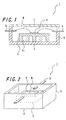
Fig. 1 is a sectional view showing one example of a package for housing a device in accordance with one embodiment of the invention; -
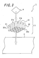
Fig. 2 is a perspective view showing one example of the package for housing the device; -
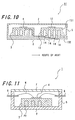
Fig. 3 is an exploded perspective view showing a support body employed in the package for housing the device; -
Fig. 4 is a sectional view showing one example of the package for housing the device as seen in a case where a notch is formed in that part of a base body which is located between columnar parts; -
Fig. 5 is an exploded perspective view showing a support body related to a modified-form example 1; -
Fig. 6 is an exploded perspective view showing a support body related to a modified-form example 2; -
Fig. 7 is an exploded perspective view showing a support body related to a modified-form example 3; -
Fig. 8 is a sectional view showing one example of a package for housing a device in accordance with a modified-form example 4; -
Fig. 9 is a sectional view showing one example of a package for housing a device in accordance with a modified-form example 5; -
Fig. 10 is a sectional view showing one example of a package for housing a device in accordance with a modified-form example 6; and -
Fig. 11 is a sectional view showing one example of a package for housing a device in accordance with a modified-form example 7. - Hereinafter, an embodiment of the invention will be described with reference to the drawings.
- As shown in
Figs. 1 and 2 , a package for housing adevice 1 in accordance with this embodiment comprises abase body 2, asupport body 3, apower semiconductor device 4, aframe body 5,power supply terminals 6, and alid body 7. Note that a diagrammatic representation of thelid body 7 is omitted inFig. 2 . Herein, thesupport body 3 and thepower semiconductor device 4 constitute one embodiment of a substrate for mounting a device according to the invention. - The
base body 2 is made, for example, of a ceramic material, a metal material, a glass material, a highly heat-resistant resin material, or the like. Examples of the ceramic material include an aluminum oxide sintered compact, a mullite sintered compact, a silicon carbide (SiC) sintered compact, an aluminum nitride sintered compact, a silicon nitride sintered compact, and glass ceramics. Moreover, examples of the metal material include a Fe-based_alloy, oxygen free copper, and SUS. Further, examples of the glass material include borosilicate glass and quartz glass. Still further, examples of the highly heat-resistant resin material include polyimide. - The
support body 3 is bonded to an upper surface of thebase body 2. Moreover, thepower semiconductor device 4 is bonded to an upper surface of the support body 3 (to be specific, a main surface of adevice mounting portion 31 which will hereafter be described). Although, in this embodiment, thepower semiconductor device 4 is an SiC-made semiconductor device, it is not limited thereto but may be a semiconductor device constructed by using silicon, gallium nitride, diamond, or the like. That is, there is no particular limitation to the type of thepower semiconductor device 4 according to the invention. Note that, in thepower semiconductor device 4 in general, its operating temperatures are so set as to fall within a range of 200°C or above and 500°C or below. - Herein, the
support body 3 related to the present embodiment supports thepower semiconductor device 4, and also has the capability of dissipating heat generated from thepower semiconductor device 4 to the outside while effecting heat insulation. For example, thesupport body 3 is made of a ceramic material, a metal material, or the like. Examples of the ceramic material include an aluminum oxide sintered compact, a mullite sintered compact, a silicon carbide sintered compact, an aluminum nitride sintered compact, a silicon nitride sintered compact, and glass ceramics. Moreover, examples of the metal material include a copper-tungsten composite material, a copper-molybdenum composite material, and copper. - As shown in
Fig. 3 , thesupport body 3 includes adevice mounting portion 31 having acolumnar part 32. Thedevice mounting portion 31 is a member having a main surface (one surface) 31a on which thepower semiconductor device 4 is to be mounted. That is, thepower semiconductor device 4 is mounted on themain surface 31a of thedevice mounting portion 31. In this way, heat generated from thepower semiconductor device 4 can be diffused by the flat plate-shapeddevice mounting portion 31. Moreover, there are provided a plurality ofcolumnar parts 32 that are each so formed as to jut out from a back surface (the other surface) 31b of thedevice mounting portion 31. Further, thebase body 2 is bonded to lowersurfaces 32a of the plurality ofcolumnar parts 32. Note that the distance between thecolumnar parts 32, the length of thecolumnar part 32, the number of thecolumnar parts 32, etc. are determined arbitrarily in an appropriate manner with consideration given to the type of thepower semiconductor device 4, device usage, and so forth. A space P1 is located between thecolumnar parts 32. - Since the
columnar part 32 is greater in thermal conductivity than the space P1, it follows that a heat accumulating region whose thermal conductivity is lower than that of thecolumnar part 32 is present between the adjacentcolumnar parts 32. Note that, for example, the thermal conductivity of thecolumnar part 32 is set to fall within a range of 1 W/(m·K) or above and 400 W/(m·K). - Moreover, in order to reduce the amount of heat traveling from the
columnar part 32 toward thebase body 2 so that thepower semiconductor device 4 can be operated within the range of operating temperatures, as a bonding material for connecting thelower surface 32a of thecolumnar part 32 and thebase body 2, for example, a silver-copper brazing material, gold-germanium solder, a ceramic adhesive, a highly heat-resistant resin adhesive, or the like is used. - As for the heat generated from the
power semiconductor device 4, while most part of the heat can be transferred from the upper area of thesupport body 3 through the lower-locatedcolumnar parts 32 to thebase body 2 successfully, a part of the heat tends to be transferred into the space P1 from the upper area of thesupport body 3 with consequent confinement of the heat in the space P1. Therefore, in a region near thepower semiconductor device 4, by decreasing the temperature of thesupport body 3, it is possible to restrain thepower semiconductor device 4 from acquiring an unduly high temperature. Moreover, in a region spaced away from thepower semiconductor device 4, namely, in a region near the space P1 located between thecolumnar parts 32, satisfactory heat accumulation can be achieved by exploiting heat generated from thepower semiconductor device 4. This makes it possible to successfully suppress too large a drop in the internal temperature of the package, as well as to successfully restrain heat emanating from the package from affecting operations of other electronic components arranged around the package. - It is noted that such a package for housing the device is used as a component of various electronic apparatuses including an inverter of a household electrical appliance and a power converter for use in a power plant and a substation, for example.
- The
frame body 5 is disposed on the upper surface of thebase body 2 so as to surround thesupport body 3 and thepower semiconductor device 4. Herein, theframe body 5 is made for example of a ceramic material, a metal material, a glass material, a highly heat-resistant resin material, or the like. Note that theframe body 5 may be either formed integrally with thebase body 2 or formed separately from thebase body 2. In a case where theframe body 5 is formed separately from thebase body 2, theframe body 5 and thebase body 2 are bonded together by means of a bonding material such as solder or a brazing material, for example. - The
power supply terminal 6 is a terminal for delivering electric power to thepower semiconductor device 4. Accordingly, thepower supply terminal 6 is electrically connected to thepower semiconductor device 4 via a wire (bonding wire) W. - The
lid body 7 is bonded to an upper surface of theframe body 5. More specifically, thelid body 7 is bonded to the upper surface of theframe body 5 by means of a bonding material such as solder, a brazing material, or the like, in such a manner that a housing space created by theframe body 5 for accommodating therein thepower semiconductor device 4 can be an enclosed space under an aerial atmosphere, an inert gas atmosphere, or a vacuum state. - As described heretofore, according to the substrate for mounting the device and the package for housing the
device 1 employing this substrate in accordance with the present embodiment, it is possible to dissipate heat generated from thepower semiconductor device 4 while effecting heat insulation with a simple structure. As a result, the substrate for mounting the device and the package for housing thedevice 1 employing this substrate in accordance with the present embodiment afford the advantage of being able to make effective use of heat generated from the power semiconductor device within the range of operating temperatures of the power semiconductor device. - It is noted that, even in the construction thus far described, depending on the type of the
power semiconductor device 4, device usage, and so forth, there is a possibility that the temperature of thepower semiconductor device 4 will exceed the operating temperatures. In light of this, as shown inFig. 4 , anotch 8 is formed in an area of thebase body 2 which is located between thecolumnar parts 32. This makes it possible to facilitate the escape of heat confined in the space P1 between thecolumnar parts 32 from the notch 8-bearing area of thebase body 2 to the outside, and thereby lower the temperature of heat generated from thepower semiconductor device 4. That is, the notch 8-bearing area of thebase body 2 is smaller in thickness than the area thereof devoid of thenotch 8. In fact, even in the construction as shown inFig. 4 , it is possible to dissipate heat generated from thepower semiconductor device 4 while effecting heat insulation with a simple structure. Note that the depth of thenotch 8, the number of thenotches 8, etc. are determined arbitrarily in an appropriate manner with consideration given to the type of thepower semiconductor device 4, device usage, and so forth. - Moreover, although the above description deals with the case where only a single
power semiconductor device 4 is placed inside the package for housing thedevice 1, the invention is not so limited. That is, the number of thepower semiconductor device 4 to be placed inside the package for housing thedevice 1 can be determined arbitrarily. Accordingly, a plurality ofsupport bodies 3 and a plurality ofpower semiconductor devices 4 attached respectively to thesupport bodies 3 can be placed inside the package for housing thedevice 1, and also asingle support body 3 and a plurality ofpower semiconductor devices 4 attached to thissupport body 3 can be placed inside the package for housing thedevice 1. - It is noted that the above-described embodiment is presented for purposes of illustration of one specific example of embodiments of the invention, and therefore various changes and modifications may be made therein. Hereafter, examples of a few main modified forms will be presented.
- By way of the above-described embodiment, as shown in
Fig. 3 , the substrate for mounting the device is described comprising thedevice mounting portion 31 having themain surface 31a on which thepower semiconductor device 4 is to be mounted, the plurality of thecolumnar parts 32 formed so as to jut out from theback surface 31b of thedevice mounting portion 31, and thebase body 2 bonded to thelower surfaces 32a of the plurality of thecolumnar parts 32. Even in this construction, however, depending on the type of thepower semiconductor device 4, device usage, and so forth, there may be a case where heat generated from thepower semiconductor device 4 is dissipated to excess. In light of this, a substrate for mounting adevice 1a in accordance with a modified-form example 1 will be explained. As shown inFig. 5 , in this example, asupport body 3a includes abottom plate 33 which is connected to thelower surfaces 32a of the plurality ofcolumnar parts 32. Note that, inFig. 5 , the components that are similar in function to those inFig. 3 will be identified with the same reference symbols, and detailed descriptions thereof will be omitted. - As shown in
Fig. 5 , thesupport body 3a related to the modified-form example 1 comprises adevice mounting portion 31,columnar parts 32, and abottom plate 33. Thedevice mounting portion 31 is a member having amain surface 31a on which thepower semiconductor device 4 is to be mounted. Moreover, there are provided the plurality ofcolumnar parts 32 that are each so formed as to jut out from aback surface 31b of thedevice mounting portion 31. Further, thebottom plate 33 is connected to thelower surfaces 32a of the plurality ofcolumnar parts 32. Still further, thebase body 2 is bonded to thebottom plate 33. - Thus, according to the substrate for mounting the device and the package for housing the
device 1a employing this substrate in accordance with the modified-form example 1, since thelower surfaces 32a of the plurality ofcolumnar parts 32 and thebottom plate 33 are connected to each other and also thebottom plate 33 and thebase body 2 are bonded to each other, it never occurs that heat generated from thepower semiconductor device 4 is directly transmitted to thebase body 2. Therefore, as compared with the preceding embodiment, in this example, heat generated from thepower semiconductor device 4 can be confined more readily in the space P1 between the columnar parts 32 (namely, a region between thedevice mounting portion 31 and the bottom plate 33). Moreover, according to the substrate for mounting the device and the package for housing thedevice 1a employing this substrate in accordance with the modified-form example 1, since there are provided the plurality ofcolumnar parts 32, it is possible to cause heat generated from thepower semiconductor device 4 to dissipate fromlateral surfaces 32b of the plurality ofcolumnar parts 32. Further, heat generated from thepower semiconductor device 4 can be dissipated also from thebase body 2 bonded to thebottom plate 33. In this way, according to the substrate for mounting the device and the package for housing thedevice 1a employing this substrate in accordance with the modified-form example 1, it is possible to insulate heat generated from thepower semiconductor device 4 more positively than may be the case of the preceding embodiment while dissipating the heat to a certain extent. - By way of the above-described modified-form example 1, as shown in
Fig. 5 , the substrate for mounting the device is described comprising the flat plate-shapeddevice mounting portion 31 having themain surface 31a on which thesemiconductor device 4 is to be mounted, the plurality ofcolumnar parts 32 formed so as to jut out from theback surface 31b of thedevice mounting portion 31, thebottom plate 33 connected to thelower surfaces 32a of the plurality ofcolumnar parts 32, and thebase body 2 bonded to thebottom plate 33. Even in this construction, however, depending on the type of thepower semiconductor device 4, device usage, and so forth, there may be a case where heat generated from thepower semiconductor device 4 is dissipated to excess. In light of this, in a substrate for mounting adevice 1b in accordance with a modified-form example 2, as shown inFig. 6 , asupport body 3b includes a surrounding portion which is connected to aback surface 31b of adevice mounting portion 31 so as to surround the plurality ofcolumnar parts 32. Herein, as exemplary of the surrounding portion, alateral plate 34 will be explained. Note that, inFig. 6 , the components that are similar in function to those inFig. 3 will be identified with the same reference symbols, and detailed descriptions thereof will be omitted. - As shown in
Fig. 6 , thesupport body 3b related to the modified-form example 2 comprises adevice mounting portion 31,columnar parts 32, and alateral plate 34. Thedevice mounting portion 31 is a member having themain surface 31a on which thepower semiconductor device 4 is to be mounted. Moreover, there are provided the plurality ofcolumnar parts 32 that are each so formed as to jut out from theback surface 31b of thedevice mounting portion 31. Further, thelateral plate 34 is connected to theback surface 31b of thedevice mounting portion 31 so as to surround the plurality ofcolumnar parts 32. Still further, thebase body 2 is bonded to thelower surfaces 32a of the plurality ofcolumnar parts 32 and alower surface 34a of thelateral plate 34 as well. - Thus, according to the substrate for mounting the device and the package for housing the
device 1b employing this substrate in accordance with the modified-form example 2, there is provided thelateral plate 34 connected to theback surface 31b of thedevice mounting portion 31 so as to surround the plurality ofcolumnar parts 32. Therefore, as compared with the modified-form example 1, in this example, heat generated from thepower semiconductor device 4 can be confined more readily in the space P1 between the columnar parts 32 (namely, a region between thedevice mounting portion 31 and the base body 2). Moreover, according to the substrate for mounting the device and the package for housing thedevice 1b employing this substrate in accordance with the modified-form example 2, heat generated from thepower semiconductor device 4 can be dissipated from thelateral plate 34 and thebase body 2. In this way, according to the substrate for mounting the device and the package for housing thedevice 1b employing this substrate in accordance with the modified-form example 2, it is possible to insulate heat generated from thepower semiconductor device 4 more positively than may be the case of the modified-form example 1 while dissipating the heat to a certain extent. - By way of the above-described modified-form example 2, as shown in
Fig. 6 , the substrate for mounting the device is described comprising the flat plate-shapeddevice mounting portion 31 having themain surface 31a on which thepower semiconductor device 4 is to be mounted, the plurality ofcolumnar parts 32 formed so as to jut out from theback surface 31b of thedevice mounting portion 31, thelateral plate 34 connected to theback surface 31b of thedevice mounting portion 4 so as to surround the plurality ofcolumnar parts 32, and thebase body 2 bonded to thelower surfaces 32a of the plurality ofcolumnar parts 32 and thelower surface 34a of thelateral plate 34 as well. Even in this construction, however, depending on the type of thepower semiconductor device 4, device usage, and so forth, there may be a case where heat generated from thepower semiconductor device 4 is dissipated to excess. In light of this, a substrate for mounting a device 1c in accordance with a modified-form example 3 will be explained. As shown inFig. 7 , in this example, a support body 3c includes abottom plate 36 which is connected to thelower surfaces 32a of the plurality ofcolumnar parts 32 and alower surface 35a of alateral plate 35 as well. Note that, inFig. 7 , the components that are similar in function to those inFig. 3 will be identified with the same reference symbols, and detailed descriptions thereof will be omitted. - As shown in
Fig. 7 , the support body 3c related to the modified-form example 3 comprises adevice mounting portion 31,columnar parts 32, alateral plate 35, and abottom plate 36. Thedevice mounting portion 31 is a member having themain surface 31a on which thepower semiconductor device 4 is to be mounted. Moreover, there are provided a plurality ofcolumnar parts 32 that are each so formed as to jut out from theback surface 31b of thedevice mounting portion 31. Moreover, thelateral plate 35 is connected to theback surface 31b of thedevice mounting portion 31 so as to surround the plurality ofcolumnar parts 32. Further, thebottom plate 36 is connected to thelower surfaces 32a of the plurality ofcolumnar parts 32 and thelower surface 35a of thelateral plate 35 as well. Still further, thebase body 2 is bonded to thebottom plate 36. - That is, according to the substrate for mounting the device and the package for housing the device 1c employing this substrate in accordance with the modified-form example 3, since the
lower surfaces 32a of the plurality ofcolumnar parts 32, thelower surface 35a of thelateral plate 35, and thebottom plate 36 are connected to one another and also thebottom plate 36 and thebase body 2 are bonded to each other, it never occurs that heat generated from thepower semiconductor device 4 is directly transmitted to thebase body 2. Moreover, with the provision of thelateral plate 35 connected to theback surface 31b of thedevice mounting portion 31 so as to surround the plurality ofcolumnar parts 32, as compared with the modified-form example 2, in this example, heat generated from thepower semiconductor device 4 can be confined more readily in the space P1 between the columnar parts 32 (namely, a region between thedevice mounting portion 31 and the bottom plate 36). Moreover, according to the substrate for mounting the device and the package for housing the device 1c employing this substrate in accordance with the modified-form example 3, heat generated from thepower semiconductor device 4 can be dissipated from thelateral plate 35 and thebase body 2. In this way, according to the substrate for mounting the device and the package for housing the device 1c employing this substrate in accordance with the modified-form example 3, it is possible to insulate heat generated from thepower semiconductor device 4 more positively than may be the case of the modified-form example 2 while dissipating the heat to a certain extent. - As shown in
Fig. 8 , a package for housing thedevice 1d in accordance with a modified-form example 4 is provided with asupport body 3d in lieu of thesupport body 3 shown inFig. 1 . Note that, inFig. 8 , the components that are similar in function to those inFig. 3 will be identified with the same reference symbols, and detailed descriptions thereof will be omitted. - As shown in
Fig. 8 , the substrate for mounting thedevice 1d in accordance with the modified-form example 4 comprises thesupport body 3d having an upper surface on which thepower semiconductor device 4 is to be mounted. Moreover, thebase body 2 related to the modified-form example 4 is bonded to the lower surface of thesupport body 3d. Further, thesupport body 3d has a plurality of pores B formed therein. Note that, in a case where thesupport body 3d is made, for example, of a ceramic material, the plurality of pores B within thesupport body 3d are formed as follows, for example. That is, a plurality of resin beads are mixed in the ceramic material in advance. Then, the ceramic material, along with the resin beads, is fired at a predetermined temperature with consequent decomposition of the resin beads. By doing so, portions where the resin beads existed become pores B, wherefore the plurality of pores B can be formed within thesupport body 3d. Note that the foregoing is cited merely by way of example and there is no particular limitation to the method of forming the pores B within thesupport body 3d. - Thus, according to the substrate for mounting the device and the package for housing the
device 1d employing this substrate in accordance with the modified-form example 4, since the plurality of pores B are formed within thesupport body 3d, it follows that heat generated from thepower semiconductor device 4 can be readily confined in the plurality of pores B formed within thesupport body 3d. Moreover, according to the substrate for mounting the device and the package for housing thedevice 1d employing this substrate in accordance with the modified-form example 4, heat generated from thepower semiconductor device 4 can be dissipated from thebase body 2 bonded to the lower surface of thesupport body 3d. In this way, according to the substrate for mounting the device and the package for housing thedevice 1d employing this substrate in accordance with the modified-form example 4, it is possible to dissipate heat generated from thepower semiconductor device 4 while effecting heat insulation with a simple structure. - It is preferable that, as shown in
Fig. 8 , thesupport body 3d is so designed that its porosity (the plurality of pores B formed within thesupport body 3d) becomes higher gradually from an area thereof on a side of thepower semiconductor device 4 to an area thereof on a side of thebase body 2. That is, the higher the porosity is, the lower the heat transmission property is (the less likely heat is transmitted easily). Accordingly, where thesupport body 3d is so designed that its porosity becomes higher gradually from a power semiconductor device 4-sided area of thesupport body 3d to a base body 2-sided area of thesupport body 3d, it is possible to contain heat generated from thepower semiconductor device 4 in the pores B located in the base body 2-sided area of thesupport body 3d, not in the pores B located in the power semiconductor device 4-sided area of thesupport body 3d. Moreover, even if heat generated from other electronic components is transmitted through thebase body 2 to thesupport body 3d, it is possible to contain the said heat in the pores B located in the base body 2-sided area of thesupport body 3d. This helps reduce the possibility that the temperature of thepower semiconductor device 4 exceeds the operating temperatures. - In the embodiment and the modified-form examples 1 to 4 thus far described, only the
support body power semiconductor device 4 are placed inside the package for housing thedevice Fig. 9 , in addition to thesupport body 3 and thepower semiconductor device 4, abase 11 and anelectronic component 12 may be placed inside a package for housing the device 1e. Thebase 11 is bonded to the upper surface of thebase body 2. Theelectronic component 12 is mounted on the upper surface of thebase 11. That is, theframe body 5 is disposed on the upper surface of thebase body 2 so as to surround thepower semiconductor device 4 and theelectronic component 12. Herein, theelectronic component 12 refers, for example, to a resistor, a piezoelectric element, a quartz oscillator, a ceramic resonator, or the like. In this way, both of thepower semiconductor device 4 and theelectronic component 12 can be placed inside the package for housing the device 1e. Note that, instead of theelectronic component 12, a semiconductor device (for example, an SiC-made semiconductor device, an Si-made semiconductor device, or a semiconductor device constructed by using gallium nitride, diamond, or the like) may be placed therein. - Although, in
Fig. 9 , there is shown the case where the support body placed inside the package for housing the device 1e is thesupport body 3 of the embodiment described above (refer toFig. 3 ), the invention is not so limited. That is, the support body placed inside the package for housing the device 1e may be any of thesupport body 3a related to the modified-form example 1 (refer toFig. 5 ), thesupport body 3b related to the modified-form example 2 (refer toFig. 6 ), the support body 3c related to the modified-form example 3 (refer toFig. 7 ), and thesupport body 3d related to the modified-form example 4 (refer toFig. 8 ). Herein, in order to restrain theelectronic component 12 from being affected by heat generated from thepower semiconductor device 4, it is desirable to use a support body which exhibits high heat insulation property. For example, thesupport body 3b related to the modified-form example 2 or the support body 3c related to the modified-form example 3 is desirable for use. - Moreover, although the above description deals with the case where only a single
electronic component 12 is placed inside the package for housing the device 1e, the invention is not so limited. That is, the number of theelectronic component 12 to be placed inside the package for housing the device 1e can be determined arbitrarily. - In
Fig. 9 representing the above-described modified-form example 5, there is shown the example in which thebase 11 has a rectangular parallelepiped shape. However, in the above-described modified-form example 5, heat generated from thepower semiconductor device 4 is transmitted to theelectronic component 12 through thesupport body 3, thebase body 2, and thebase 11. Therefore, theelectronic component 12 is significantly affected by the heat generated from thepower semiconductor device 4. This gives rise to a possibility that theelectronic component 12 suffers from troubles due to the heat generated from thepower semiconductor device 4. In light of this, a modified-form example 6 will be explained. In this example, as shown inFig. 10 , anotch 14 is formed in an area of thebase body 2 which is located between thecolumnar parts 32. Note that a semiconductor device (for example, an SiC-made semiconductor device, an Si-made semiconductor device, or a semiconductor device constructed by using gallium nitride, diamond, or the like) may be used in lieu of theelectronic component 12. - As shown in
Fig. 10 , in a device housing package 1f in accordance with the modified-form example 6, abase 13 comprises a flat plate-shaped electronic-component mounting portion 131 having a main surface (one surface) on which theelectronic component 12 is to be mounted, and a plurality ofcolumnar parts 132 formed so as to jut out from the back surface (the other surface) of the electronic-component mounting portion 131. Moreover, thebase body 2 is bonded to the lower surfaces of the plurality ofcolumnar parts 132. - Herein, a
notch 14 is formed in an area of thebase body 2 which is located between thecolumnar parts 32. Thenotches 14 are so formed as to be arranged in order of increasing depth in the direction of thickness of thebase body 2 along a direction away from thepower semiconductor device 4. In this way, as indicated by an arrow depicted inFig. 10 (the route of heat), it is possible to facilitate the escape of heat generated from thepower semiconductor device 4 from thebase body 2 below thenotches 14 to the outside of the device housing package 1f. Hence, according to the device housing package 1f in accordance with the modified-form example 6, theelectronic component 12 can be restrained from being affected by the heat generated from thepower semiconductor device 4. - By way of the embodiment described.earlier, as shown in
Fig. 3 , the substrate for mounting the device is described comprising thedevice mounting portion 31 having themain surface 31a on which thepower semiconductor device 4 is to be mounted, the plurality ofcolumnar parts 32 formed so as to jut out from theback surface 31b of thedevice mounting portion 31, and thebase body 2 bonded to thelower surfaces 32a of the plurality ofcolumnar parts 32. Even in this construction, however, depending on the type of thepower semiconductor device 4, device usage, and so forth, there may be a case where heat generated from thepower semiconductor device 4 is dissipated to excess. In light of this, in adevice housing package 1d in accordance with a modified-form example 7, as shown inFig. 11 , instead of the space P1 is present between the columnar parts as shown inFig. 1 , a thermal insulating material P2 is disposed between the columnar parts. Note that, inFig. 11 , the components that are similar in function to those inFig. 3 will be identified with the same reference symbols, and detailed descriptions thereof will be omitted. - As shown in
Fig. 11 , asupport body 3a related to the modified-form example 7 comprises adevice mounting portion 31 andcolumnar parts 32. Thedevice mounting portion 31 is a member having themain surface 31a on which thepower semiconductor device 4 is to be mounted. Moreover, there are provided a plurality ofcolumnar parts 32 that are each so formed as to jut out from theback surface 31b of thedevice mounting portion 31. Moreover, abottom plate 33 is connected to thelower surfaces 32a of the plurality ofcolumnar parts 32. Further, thebase body 2 is bonded to thebottom plate 33. Still further, the thermal insulating material P2 is disposed between thecolumnar parts 32. - The thermal insulating material P2 is made of a material which is lower in thermal conductivity than the
columnar part 32. The thermal insulating material P2 is made, for example, of a glass material, a highly heat-resistant resin material, or the like that has been processed into a fiber form or a bubble-bearing form. For example, the thermal conductivity of the thermal insulating material P2 is set to fall within a range of 0.02 W/(m·K) or above and 2 W/(m·K) or below. - Thus, according to the substrate for mounting the device and the
package 1a for housing the device employing this substrate in accordance with the modified-form example 7, since the thermal insulating material P2 is disposed between the adjacent ones of the plurality ofcolumnar parts 32, it never occurs that heat generated from thepower semiconductor device 4 is directly transmitted to thebase body 2. Therefore, as compared with the preceding examples, heat generated from thepower semiconductor device 4 can be confined more readily in the thermal insulating material P2 between the columnar parts 32 (namely, a region between thedevice mounting portion 31 and the bottom plate 33). Hence, according to the substrate for mounting the device and the package for housing thedevice 1a employing this substrate in accordance with the modified-form example 1, it is possible to keep heat generated from thepower semiconductor device 4 within the package for housing thedevice 1a more reliably than may be the case of the preceding embodiment.
Claims (8)
- A substrate for mounting a device comprising:a support body having, on one main surface of the support body, a device mounting portion for mounting a power semiconductor device, the support body having a plurality of columnar parts that are spaced apart in a thickness direction with respect to a mounting surface and are arranged apart from each other; anda heat accumulating region which is disposed between the columnar parts and is lower in thermal conductivity than the support body.
- The substrate for mounting the device according to claim 1, further comprising:a base body bonded to the support body at the columnar parts,wherein a notch is formed in an area of the base body which is located between the columnar parts.
- The substrate for mounting the device according to claim 1 or 2, wherein the support body further includes a surrounding portion formed so as to surround the plurality of columnar parts.
- A substrate for mounting a device comprising:a support body having an upper surface on which a power semiconductor device is to be mounted; anda base body bonded to a lower surface of the support body,the support body having a plurality of pores formed therein.
- The substrate for mounting the device according to claim 4, wherein the support body is so designed that a porosity of the plurality of pores formed therein becomes higher gradually from a power semiconductor device-sided area of the support body to a base body-sided area of the support body.
- The substrate for mounting the device according to any one of claims 1 to 5, wherein the power semiconductor device is a semiconductor device comprising SiC.
- A package for housing the device comprising:the substrate according to any one of claims 1 to 6;a frame body which accommodates therein the substrate and is so placed as to surround the power semiconductor device; anda lid body bonded to an upper surface of the frame body.
- The package for housing the device according to claim 7, further comprising a base which is provided within the frame body and on which an electronic component is to be mounted.
Applications Claiming Priority (3)
| Application Number | Priority Date | Filing Date | Title |
|---|---|---|---|
| JP2009011751 | 2009-01-22 | ||
| JP2009105165 | 2009-04-23 | ||
| PCT/JP2010/050809 WO2010084955A1 (en) | 2009-01-22 | 2010-01-22 | Board for mounting component, and package for holding component using same |
Publications (2)
| Publication Number | Publication Date |
|---|---|
| EP2390910A1 true EP2390910A1 (en) | 2011-11-30 |
| EP2390910A4 EP2390910A4 (en) | 2015-04-22 |
Family
ID=42356005
Family Applications (1)
| Application Number | Title | Priority Date | Filing Date |
|---|---|---|---|
| EP10733562.2A Withdrawn EP2390910A4 (en) | 2009-01-22 | 2010-01-22 | COMPONENT MOUNTING CARD, AND COMPONENT MAINTAINING BOX USING THE SAME |
Country Status (5)
| Country | Link |
|---|---|
| US (1) | US8837164B2 (en) |
| EP (1) | EP2390910A4 (en) |
| JP (1) | JP5484338B2 (en) |
| CN (1) | CN101925998B (en) |
| WO (1) | WO2010084955A1 (en) |
Families Citing this family (3)
| Publication number | Priority date | Publication date | Assignee | Title |
|---|---|---|---|---|
| JP5921723B2 (en) * | 2013-01-11 | 2016-05-24 | 三菱電機株式会社 | Semiconductor device |
| JP6099085B2 (en) * | 2013-01-24 | 2017-03-22 | 国立研究開発法人物質・材料研究機構 | Method of manufacturing nitride semiconductor device |
| US10015907B2 (en) * | 2016-03-23 | 2018-07-03 | Amulaire Thermal Technology, Inc. | Heat dissipating device |
Family Cites Families (33)
| Publication number | Priority date | Publication date | Assignee | Title |
|---|---|---|---|---|
| US4354720A (en) * | 1980-10-20 | 1982-10-19 | Amp Incorporated | Connector assembly having improved latching means |
| US4620216A (en) * | 1983-04-29 | 1986-10-28 | International Business Machines Corporation | Unitary slotted heat sink for semiconductor packages |
| US5144412A (en) * | 1987-02-19 | 1992-09-01 | Olin Corporation | Process for manufacturing plastic pin grid arrays and the product produced thereby |
| US4965227A (en) * | 1987-05-21 | 1990-10-23 | Olin Corporation | Process for manufacturing plastic pin grid arrays and the product produced thereby |
| EP0434264B1 (en) * | 1989-12-22 | 1994-10-12 | Westinghouse Electric Corporation | Package for power semiconductor components |
| US5148265A (en) * | 1990-09-24 | 1992-09-15 | Ist Associates, Inc. | Semiconductor chip assemblies with fan-in leads |
| US5158912A (en) * | 1991-04-09 | 1992-10-27 | Digital Equipment Corporation | Integral heatsink semiconductor package |
| US5206460A (en) * | 1991-07-24 | 1993-04-27 | Yang Mu K | Oscillator package |
| JPH0567658A (en) * | 1991-09-09 | 1993-03-19 | Advantest Corp | Ic carrier |
| US5736787A (en) * | 1996-07-11 | 1998-04-07 | Larimer; William R. | Transistor package structured to provide heat dissipation enabling use of silicon carbide transistors and other high power semiconductor devices |
| JPH11111898A (en) * | 1997-10-06 | 1999-04-23 | Zojirushi Vacuum Bottle Co | Cooling device for semiconductor device |
| US5930666A (en) * | 1997-10-09 | 1999-07-27 | Astralux, Incorporated | Method and apparatus for packaging high temperature solid state electronic devices |
| KR100259080B1 (en) * | 1998-02-11 | 2000-06-15 | 김영환 | Lead frame having heat spread and semiconductor package with such lead frame |
| US6667664B2 (en) * | 2000-01-31 | 2003-12-23 | Kinseki Limited | Container for oscillation circuit using piezoelectric vibrator, manufacturing method therefor, and oscillator |
| US6683368B1 (en) * | 2000-06-09 | 2004-01-27 | National Semiconductor Corporation | Lead frame design for chip scale package |
| US6292367B1 (en) * | 2000-06-22 | 2001-09-18 | International Business Machines Corporation | Thermally efficient semiconductor chip |
| US6541310B1 (en) * | 2000-07-24 | 2003-04-01 | Siliconware Precision Industries Co., Ltd. | Method of fabricating a thin and fine ball-grid array package with embedded heat spreader |
| US6894903B2 (en) * | 2001-02-28 | 2005-05-17 | Sumitomo Electric Industries, Ltd. | Optical data link |
| JP2004296726A (en) * | 2003-03-26 | 2004-10-21 | Kyocera Corp | Heat radiating member, package for storing semiconductor element, and semiconductor device |
| US6921971B2 (en) | 2003-01-15 | 2005-07-26 | Kyocera Corporation | Heat releasing member, package for accommodating semiconductor element and semiconductor device |
| JP4133635B2 (en) * | 2003-07-09 | 2008-08-13 | 株式会社豊田自動織機 | Electrical equipment system, electrical equipment module cooling device and porous radiator for the cooling equipment |
| US20050110168A1 (en) * | 2003-11-20 | 2005-05-26 | Texas Instruments Incorporated | Low coefficient of thermal expansion (CTE) semiconductor packaging materials |
| US7196907B2 (en) * | 2004-02-09 | 2007-03-27 | Wen-Chun Zheng | Elasto-plastic sockets for Land or Ball Grid Array packages and subsystem assembly |
| JP2006294890A (en) | 2005-04-12 | 2006-10-26 | Nissan Motor Co Ltd | Semiconductor device and manufacturing method thereof |
| JP4568202B2 (en) * | 2005-09-29 | 2010-10-27 | Okiセミコンダクタ株式会社 | Semiconductor device |
| JP4811936B2 (en) * | 2006-08-02 | 2011-11-09 | オムロンオートモーティブエレクトロニクス株式会社 | Electronic device manufacturing method, electronic device |
| JP5000660B2 (en) * | 2006-09-27 | 2012-08-15 | 京セラ株式会社 | CAPACITOR DEVICE, ELECTRONIC COMPONENT, FILTER DEVICE, COMMUNICATION DEVICE, AND CAPACITOR DEVICE MANUFACTURING METHOD |
| US20080130935A1 (en) * | 2006-09-27 | 2008-06-05 | Yamaha Corporation | Microphone package |
| JP4957208B2 (en) | 2006-11-28 | 2012-06-20 | 三菱マテリアル株式会社 | Power module substrate with heat sink and power module |
| JP4385058B2 (en) * | 2007-05-07 | 2009-12-16 | 三菱電機株式会社 | Electronic control unit |
| US20100019379A1 (en) * | 2008-07-24 | 2010-01-28 | Broadcom Corporation | External heat sink for bare-die flip chip packages |
| US8791471B2 (en) * | 2008-11-07 | 2014-07-29 | Cree Hong Kong Limited | Multi-chip light emitting diode modules |
| US8368112B2 (en) * | 2009-01-14 | 2013-02-05 | Cree Huizhou Opto Limited | Aligned multiple emitter package |
-
2010
- 2010-01-22 US US12/865,107 patent/US8837164B2/en not_active Expired - Fee Related
- 2010-01-22 JP JP2010527686A patent/JP5484338B2/en not_active Expired - Fee Related
- 2010-01-22 WO PCT/JP2010/050809 patent/WO2010084955A1/en not_active Ceased
- 2010-01-22 CN CN2010800010272A patent/CN101925998B/en not_active Expired - Fee Related
- 2010-01-22 EP EP10733562.2A patent/EP2390910A4/en not_active Withdrawn
Also Published As
| Publication number | Publication date |
|---|---|
| EP2390910A4 (en) | 2015-04-22 |
| WO2010084955A1 (en) | 2010-07-29 |
| US20110273846A1 (en) | 2011-11-10 |
| JPWO2010084955A1 (en) | 2012-07-19 |
| CN101925998A (en) | 2010-12-22 |
| US8837164B2 (en) | 2014-09-16 |
| JP5484338B2 (en) | 2014-05-07 |
| CN101925998B (en) | 2012-06-27 |
Similar Documents
| Publication | Publication Date | Title |
|---|---|---|
| CN111446217B (en) | Semiconductor device with a semiconductor device having a plurality of semiconductor chips | |
| KR101325373B1 (en) | Package for housing semiconductor element and semiconductor device using the same | |
| US8847381B2 (en) | Semiconductor element housing package and semiconductor device equipped with the same | |
| CN110957278B (en) | Package for mounting electronic components and electronic device using same | |
| US8837164B2 (en) | Substrate for mounting device and package for housing device employing the same | |
| JP2015225873A (en) | Semiconductor element storage package and semiconductor device including the same | |
| US8981545B2 (en) | Explosion-protected semiconductor module | |
| US20080224570A1 (en) | Transformer Arrangement Having a Piezoelectric Transformer | |
| US11101784B2 (en) | Electrical component with heat dissipation | |
| CN106415821B (en) | Component housing package and mounting structure | |
| CN117334652A (en) | Integrated voltage regulator | |
| JP6075597B2 (en) | Device storage package and mounting structure | |
| JP2015065555A (en) | Crystal device | |
| JP2018184337A (en) | Ceramic plate and electronic device | |
| JP2017045959A (en) | High frequency semiconductor device package and high frequency semiconductor device | |
| JP2006013420A (en) | Electronic component storage package and electronic device | |
| KR20170130179A (en) | Insulating substrate using thick film printing | |
| JP6162520B2 (en) | Package for housing semiconductor element and mounting structure including the same | |
| JP5791263B2 (en) | Electronic component storage package and mounting structure | |
| JP2014049563A (en) | Package for housing electronic component and mounting structure | |
| JP5773851B2 (en) | Electronic component storage package and electronic device | |
| JP2014027158A (en) | Package for housing element and packaging structure | |
| JP2020158375A (en) | Aluminum nitride substrate, electronic device and electronic module | |
| JP2013157492A (en) | Package for housing element and packaging structure | |
| JPH0547953A (en) | Package for semiconductor device |
Legal Events
| Date | Code | Title | Description |
|---|---|---|---|
| PUAI | Public reference made under article 153(3) epc to a published international application that has entered the european phase |
Free format text: ORIGINAL CODE: 0009012 |
|
| 17P | Request for examination filed |
Effective date: 20110822 |
|
| AK | Designated contracting states |
Kind code of ref document: A1 Designated state(s): AT BE BG CH CY CZ DE DK EE ES FI FR GB GR HR HU IE IS IT LI LT LU LV MC MK MT NL NO PL PT RO SE SI SK SM TR |
|
| DAX | Request for extension of the european patent (deleted) | ||
| RA4 | Supplementary search report drawn up and despatched (corrected) |
Effective date: 20150323 |
|
| RIC1 | Information provided on ipc code assigned before grant |
Ipc: H01L 23/36 20060101AFI20150317BHEP |
|
| GRAP | Despatch of communication of intention to grant a patent |
Free format text: ORIGINAL CODE: EPIDOSNIGR1 |
|
| STAA | Information on the status of an ep patent application or granted ep patent |
Free format text: STATUS: GRANT OF PATENT IS INTENDED |
|
| INTG | Intention to grant announced |
Effective date: 20180903 |
|
| STAA | Information on the status of an ep patent application or granted ep patent |
Free format text: STATUS: THE APPLICATION IS DEEMED TO BE WITHDRAWN |
|
| 18D | Application deemed to be withdrawn |
Effective date: 20190115 |