EP2383796A1 - Solarzellenmodul - Google Patents
Solarzellenmodul Download PDFInfo
- Publication number
- EP2383796A1 EP2383796A1 EP09834735A EP09834735A EP2383796A1 EP 2383796 A1 EP2383796 A1 EP 2383796A1 EP 09834735 A EP09834735 A EP 09834735A EP 09834735 A EP09834735 A EP 09834735A EP 2383796 A1 EP2383796 A1 EP 2383796A1
- Authority
- EP
- European Patent Office
- Prior art keywords
- photoelectric conversion
- conversion element
- photovoltaic module
- insulating sheet
- sheet
- Prior art date
- Legal status (The legal status is an assumption and is not a legal conclusion. Google has not performed a legal analysis and makes no representation as to the accuracy of the status listed.)
- Withdrawn
Links
- 238000006243 chemical reaction Methods 0.000 claims abstract description 220
- 238000007789 sealing Methods 0.000 claims abstract description 61
- 238000009413 insulation Methods 0.000 claims abstract description 52
- 230000001681 protective effect Effects 0.000 claims abstract description 42
- 239000000758 substrate Substances 0.000 claims abstract description 37
- 238000004519 manufacturing process Methods 0.000 claims description 14
- 230000003287 optical effect Effects 0.000 claims description 4
- 230000003014 reinforcing effect Effects 0.000 abstract description 30
- CNQCVBJFEGMYDW-UHFFFAOYSA-N lawrencium atom Chemical compound [Lr] CNQCVBJFEGMYDW-UHFFFAOYSA-N 0.000 description 135
- 238000000034 method Methods 0.000 description 33
- 239000000463 material Substances 0.000 description 29
- 229910021417 amorphous silicon Inorganic materials 0.000 description 16
- 229920005989 resin Polymers 0.000 description 15
- 239000011347 resin Substances 0.000 description 15
- 238000010586 diagram Methods 0.000 description 14
- 239000010408 film Substances 0.000 description 13
- 239000011521 glass Substances 0.000 description 11
- 239000000853 adhesive Substances 0.000 description 9
- 230000001070 adhesive effect Effects 0.000 description 9
- 238000012360 testing method Methods 0.000 description 9
- 229910000831 Steel Inorganic materials 0.000 description 7
- 239000005038 ethylene vinyl acetate Substances 0.000 description 7
- 229920001200 poly(ethylene-vinyl acetate) Polymers 0.000 description 7
- 239000010959 steel Substances 0.000 description 7
- 238000011156 evaluation Methods 0.000 description 6
- CURLTUGMZLYLDI-UHFFFAOYSA-N Carbon dioxide Chemical compound O=C=O CURLTUGMZLYLDI-UHFFFAOYSA-N 0.000 description 4
- 238000013459 approach Methods 0.000 description 4
- 230000000052 comparative effect Effects 0.000 description 4
- YCKRFDGAMUMZLT-UHFFFAOYSA-N Fluorine atom Chemical compound [F] YCKRFDGAMUMZLT-UHFFFAOYSA-N 0.000 description 3
- 239000004642 Polyimide Substances 0.000 description 3
- 229910052731 fluorine Inorganic materials 0.000 description 3
- 239000011737 fluorine Substances 0.000 description 3
- 238000010438 heat treatment Methods 0.000 description 3
- -1 polyethylene Polymers 0.000 description 3
- 229920001721 polyimide Polymers 0.000 description 3
- XUIMIQQOPSSXEZ-UHFFFAOYSA-N Silicon Chemical compound [Si] XUIMIQQOPSSXEZ-UHFFFAOYSA-N 0.000 description 2
- LEVVHYCKPQWKOP-UHFFFAOYSA-N [Si].[Ge] Chemical compound [Si].[Ge] LEVVHYCKPQWKOP-UHFFFAOYSA-N 0.000 description 2
- 229910002092 carbon dioxide Inorganic materials 0.000 description 2
- 239000001569 carbon dioxide Substances 0.000 description 2
- 150000001875 compounds Chemical class 0.000 description 2
- 239000013078 crystal Substances 0.000 description 2
- 230000000694 effects Effects 0.000 description 2
- 239000000284 extract Substances 0.000 description 2
- 229910021424 microcrystalline silicon Inorganic materials 0.000 description 2
- 238000012986 modification Methods 0.000 description 2
- 230000004048 modification Effects 0.000 description 2
- 229920001225 polyester resin Polymers 0.000 description 2
- 239000004645 polyester resin Substances 0.000 description 2
- 238000003825 pressing Methods 0.000 description 2
- 229910052710 silicon Inorganic materials 0.000 description 2
- 239000010703 silicon Substances 0.000 description 2
- 239000010409 thin film Substances 0.000 description 2
- XLYOFNOQVPJJNP-UHFFFAOYSA-N water Substances O XLYOFNOQVPJJNP-UHFFFAOYSA-N 0.000 description 2
- PZWQOGNTADJZGH-SNAWJCMRSA-N (2e)-2-methylpenta-2,4-dienoic acid Chemical compound OC(=O)C(/C)=C/C=C PZWQOGNTADJZGH-SNAWJCMRSA-N 0.000 description 1
- 229920000178 Acrylic resin Polymers 0.000 description 1
- 239000004925 Acrylic resin Substances 0.000 description 1
- 239000004812 Fluorinated ethylene propylene Substances 0.000 description 1
- 229920000106 Liquid crystal polymer Polymers 0.000 description 1
- 239000004977 Liquid-crystal polymers (LCPs) Substances 0.000 description 1
- 239000007977 PBT buffer Substances 0.000 description 1
- 239000002033 PVDF binder Substances 0.000 description 1
- 239000004813 Perfluoroalkoxy alkane Substances 0.000 description 1
- 239000004952 Polyamide Substances 0.000 description 1
- 239000004962 Polyamide-imide Substances 0.000 description 1
- 239000004697 Polyetherimide Substances 0.000 description 1
- 239000004698 Polyethylene Substances 0.000 description 1
- 229920002873 Polyethylenimine Polymers 0.000 description 1
- 239000004734 Polyphenylene sulfide Substances 0.000 description 1
- 239000004743 Polypropylene Substances 0.000 description 1
- 229910000577 Silicon-germanium Inorganic materials 0.000 description 1
- XAGFODPZIPBFFR-UHFFFAOYSA-N aluminium Chemical compound [Al] XAGFODPZIPBFFR-UHFFFAOYSA-N 0.000 description 1
- 229910052782 aluminium Inorganic materials 0.000 description 1
- 238000009826 distribution Methods 0.000 description 1
- 239000007772 electrode material Substances 0.000 description 1
- 229920006228 ethylene acrylate copolymer Polymers 0.000 description 1
- 238000003475 lamination Methods 0.000 description 1
- 230000031700 light absorption Effects 0.000 description 1
- 238000005259 measurement Methods 0.000 description 1
- 238000013086 organic photovoltaic Methods 0.000 description 1
- 229920009441 perflouroethylene propylene Polymers 0.000 description 1
- 229920011301 perfluoro alkoxyl alkane Polymers 0.000 description 1
- 229920003207 poly(ethylene-2,6-naphthalate) Polymers 0.000 description 1
- 229920002037 poly(vinyl butyral) polymer Polymers 0.000 description 1
- 229920002647 polyamide Polymers 0.000 description 1
- 229920002312 polyamide-imide Polymers 0.000 description 1
- 229920001707 polybutylene terephthalate Polymers 0.000 description 1
- 229920000515 polycarbonate Polymers 0.000 description 1
- 239000004417 polycarbonate Substances 0.000 description 1
- 229920001601 polyetherimide Polymers 0.000 description 1
- 229920000573 polyethylene Polymers 0.000 description 1
- 239000011112 polyethylene naphthalate Substances 0.000 description 1
- 229920000139 polyethylene terephthalate Polymers 0.000 description 1
- 239000005020 polyethylene terephthalate Substances 0.000 description 1
- 229920000069 polyphenylene sulfide Polymers 0.000 description 1
- 229920001155 polypropylene Polymers 0.000 description 1
- 239000004810 polytetrafluoroethylene Substances 0.000 description 1
- 229920001343 polytetrafluoroethylene Polymers 0.000 description 1
- 229920002620 polyvinyl fluoride Polymers 0.000 description 1
- 229920002981 polyvinylidene fluoride Polymers 0.000 description 1
- 239000004065 semiconductor Substances 0.000 description 1
- 150000003376 silicon Chemical class 0.000 description 1
- HBMJWWWQQXIZIP-UHFFFAOYSA-N silicon carbide Chemical compound [Si+]#[C-] HBMJWWWQQXIZIP-UHFFFAOYSA-N 0.000 description 1
- 229910010271 silicon carbide Inorganic materials 0.000 description 1
- 229920005992 thermoplastic resin Polymers 0.000 description 1
- 229920001187 thermosetting polymer Polymers 0.000 description 1
- 238000010792 warming Methods 0.000 description 1
Images


Classifications
-
- H—ELECTRICITY
- H02—GENERATION; CONVERSION OR DISTRIBUTION OF ELECTRIC POWER
- H02S—GENERATION OF ELECTRIC POWER BY CONVERSION OF INFRARED RADIATION, VISIBLE LIGHT OR ULTRAVIOLET LIGHT, e.g. USING PHOTOVOLTAIC [PV] MODULES
- H02S20/00—Supporting structures for PV modules
- H02S20/20—Supporting structures directly fixed to an immovable object
- H02S20/22—Supporting structures directly fixed to an immovable object specially adapted for buildings
- H02S20/23—Supporting structures directly fixed to an immovable object specially adapted for buildings specially adapted for roof structures
-
- H—ELECTRICITY
- H01—ELECTRIC ELEMENTS
- H01L—SEMICONDUCTOR DEVICES NOT COVERED BY CLASS H10
- H01L31/00—Semiconductor devices sensitive to infrared radiation, light, electromagnetic radiation of shorter wavelength or corpuscular radiation and specially adapted either for the conversion of the energy of such radiation into electrical energy or for the control of electrical energy by such radiation; Processes or apparatus specially adapted for the manufacture or treatment thereof or of parts thereof; Details thereof
- H01L31/04—Semiconductor devices sensitive to infrared radiation, light, electromagnetic radiation of shorter wavelength or corpuscular radiation and specially adapted either for the conversion of the energy of such radiation into electrical energy or for the control of electrical energy by such radiation; Processes or apparatus specially adapted for the manufacture or treatment thereof or of parts thereof; Details thereof adapted as photovoltaic [PV] conversion devices
- H01L31/042—PV modules or arrays of single PV cells
- H01L31/048—Encapsulation of modules
-
- Y—GENERAL TAGGING OF NEW TECHNOLOGICAL DEVELOPMENTS; GENERAL TAGGING OF CROSS-SECTIONAL TECHNOLOGIES SPANNING OVER SEVERAL SECTIONS OF THE IPC; TECHNICAL SUBJECTS COVERED BY FORMER USPC CROSS-REFERENCE ART COLLECTIONS [XRACs] AND DIGESTS
- Y02—TECHNOLOGIES OR APPLICATIONS FOR MITIGATION OR ADAPTATION AGAINST CLIMATE CHANGE
- Y02B—CLIMATE CHANGE MITIGATION TECHNOLOGIES RELATED TO BUILDINGS, e.g. HOUSING, HOUSE APPLIANCES OR RELATED END-USER APPLICATIONS
- Y02B10/00—Integration of renewable energy sources in buildings
- Y02B10/10—Photovoltaic [PV]
-
- Y—GENERAL TAGGING OF NEW TECHNOLOGICAL DEVELOPMENTS; GENERAL TAGGING OF CROSS-SECTIONAL TECHNOLOGIES SPANNING OVER SEVERAL SECTIONS OF THE IPC; TECHNICAL SUBJECTS COVERED BY FORMER USPC CROSS-REFERENCE ART COLLECTIONS [XRACs] AND DIGESTS
- Y02—TECHNOLOGIES OR APPLICATIONS FOR MITIGATION OR ADAPTATION AGAINST CLIMATE CHANGE
- Y02E—REDUCTION OF GREENHOUSE GAS [GHG] EMISSIONS, RELATED TO ENERGY GENERATION, TRANSMISSION OR DISTRIBUTION
- Y02E10/00—Energy generation through renewable energy sources
- Y02E10/50—Photovoltaic [PV] energy
Definitions
- the present invention relates to a photovoltaic module with high insulation and weather resistance.
- photovoltaic device In recent years, global warming has been caused by the greenhouse effect due to an increase in carbon dioxide and a photovoltaic device has drawn attention as a clean energy source that does not emit carbon dioxide.
- the photovoltaic device include a crystal type photovoltaic device, an amorphous photovoltaic device, and a compound semiconductor photovoltaic device, and various kinds of photovoltaic devices have been studied and developed.
- the amorphous silicon photovoltaic device has energy conversion efficiency lower than the crystal type photovoltaic device, but has the following advantages as compared to the other photovoltaic devices: it is easy to increase the area of the amorphous silicon photovoltaic device; the amorphous silicon photovoltaic device has a large light absorption coefficient; and the amorphous silicon photovoltaic device is formed of a thin film. Therefore, the amorphous silicon photovoltaic device has good prospects.
- the amorphous silicon photovoltaic device has been widely used in the form of a photovoltaic module in which the photoelectric conversion element is sealed with a resin such that the photovoltaic module can be used outdoors for a long time.
- the amorphous silicon photovoltaic module it is possible to reduce the thickness of the substrate and reduce the weight of the photovoltaic module. Therefore, for example, when the photovoltaic module is installed on the roof of a building, it is possible to reduce a load applied to the building.
- amorphous silicon photovoltaic module when the photoelectric conversion element is manufactured, stress is applied the substrate. Therefore, during sealing, the end of the substrate is warped and the substrate comes into contact with the protective member, which results in a reduction in insulation resistance.
- the photovoltaic module has a sufficient performance immediately after the photovoltaic module is manufactured. However, when the photovoltaic module is used outdoors for a long time, the end of the substrate is warped little by little and the insulation resistance is reduced.
- a photovoltaic module has been proposed in which a glass nonwoven or a sheet member is provided on the entire surface of a photoelectric conversion element to prevent the deformation of a substrate, thereby preventing a reduction in insulation resistance (for example, see Patent Document 1).
- Patent Document 1 Japanese Patent Application Laid-Open (JP-A) No. 10-27920
- the photovoltaic module when the glass nonwoven is used, water is diffused through the interface of the sealing member or the glass nonwoven, which causes a reduction in insulation resistance.
- the sheet member when the sheet member is used, the sheet member is wrinkled by thermal expansion and the effect of preventing a reduction in insulation resistance is reduced.
- the invention has been made in view of the above-mentioned problems and an object of the invention is to provide a photovoltaic module capable of preventing a reduction in insulation resistance.
- a photovoltaic module includes a photoelectric conversion element including a flexible substrate and a photoelectric conversion layer that is formed on the flexible substrate, protective members that are provided on both surfaces of the photoelectric conversion element and are adhered to the photoelectric conversion element with sealing members interposed therebetween, and a sheet that is provided between the photoelectric conversion element and at least one of the protective members and has rigidity and insulation higher than those of the sealing member under manufacturing conditions of the photovoltaic module and installed conditions for use of the photovoltaic module.
- the sheet may be arranged on the side to which at least four corners of the photoelectric conversion element are warped at positions including the four corners.
- the insulating sheet is arranged at the four corners of the photoelectric conversion element where the photoelectric conversion element is largely warped. Therefore, it is possible to prevent a reduction in the insulation performance of the photovoltaic module without arranging the sheet on the entire surface of the photoelectric conversion element and thus reduce the area of the insulating sheet to be arranged.
- the sheet may be arranged on the side to which the four corners of the photoelectric conversion element are warped at positions including each side of both ends of the photoelectric conversion element in the longitudinal direction.
- the insulating sheet is arranged so as to include each side of both ends of the photoelectric conversion element in the longitudinal direction where the photoelectric conversion element is largely warped. Therefore, it is possible to prevent a reduction in the insulation resistance of the photovoltaic module without arranging the sheet on the entire surface of the photoelectric conversion element and thus reduce the area of the insulating sheet to be arranged.
- the sheet may be arranged on the side to which the four corners of the photoelectric conversion element are warped at the positions including each side of both ends of the photoelectric conversion element in the longitudinal direction and may be arranged between the protective member and the sealing member.
- the insulating sheet is arranged so as to include each side of both ends of the photoelectric conversion element in the longitudinal direction where the photoelectric conversion element is largely warped. Therefore, it is possible to prevent a reduction in the insulation resistance of the photovoltaic module without arranging the sheet on the entire surface of the photoelectric conversion element and thus reduce the area of the insulating sheet to be arranged.
- the sheet may have optical transparency and may be provided on a light incident surface of the photoelectric conversion element.
- the insulating sheet having optical transparency is arranged on the light incident surface. Therefore, even when the photoelectric conversion element is warped to the light incident surface, it is possible to prevent a reduction in insulation resistance.
- the sheet may be provided on a protruding portion of the photoelectric conversion element when the photoelectric conversion element is warped.
- the insulating sheet is provided on the protruding portion of the photoelectric conversion element when the photoelectric conversion element is warped. Therefore, it is possible to effectively prevent a reduction in the insulation resistance of the photoelectric conversion element.
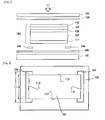
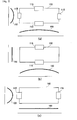
- Fig. 1 is a diagram illustrating an example of the laminated structure of a photovoltaic module according to an embodiment of the invention.
- the photovoltaic module according to this embodiment includes a protective member 101 that protects a light incident surface (hereinafter, referred to as the upper surface) of the photovoltaic module represented by an arrow in Fig.
- a reinforcing member 102 that protects a surface (hereinafter, referred to as the lower surface) opposite to the light incident surface of the photovoltaic module, and a photoelectric conversion element 103 that is provided between the protective member 101 and the reinforcing member 102 and converts sunlight into a current.
- Two insulating sheets 104 are provided at both ends of the photoelectric conversion element 103 between the photoelectric conversion element 103 and the reinforcing member 102 and insulate the photoelectric conversion element 103 from the reinforcing member 102.
- a sealing member 105 is provided between the photoelectric conversion element 103 and the protective member 101 and a sealing member 106 is provided between the insulating sheets 104 and the reinforcing member 102.
- the protective member 101 and the reinforcing member 102 may be made of any material capable of protecting the photovoltaic module.
- the protective member 101 and the reinforcing member 102 may be made of the same material or different materials.
- An electrode 108 that extracts a positive (or negative) charge subjected to photoelectric conversion, a photoelectric conversion layer 109 that converts sunlight into an electric signal, and a transparent electrode 110 that extracts a negative (or positive) charge subjected to photoelectric conversion are sequentially laminated on the upper surface of a substrate 107 of the photoelectric conversion element 103 from the upper surface of the substrate 107.
- a connection electrode 111 that connects the electrode 108 and the transparent electrode 110 is formed on the lower surface of the substrate 107.
- Fig. 2 is a plan view illustrating the arrangement of the insulating sheets 104 in the photovoltaic module according to the embodiment of the invention.
- the protective member 101, the sealing member 105, and the reinforcing member 102 are not shown in Fig. 2 .
- the sealing member 106 has a rectangular shape in a plan view and the rectangular photoelectric conversion element 103 is laminated inside the sealing member 106 in a plan view.
- the photoelectric conversion element 103 is arranged such that the longitudinal direction of the sealing member 106 is substantially parallel to the longitudinal direction of the photoelectric conversion element 103.
- the two insulating sheets 104 having a rectangular shape in a plan view are provided at both ends of the photoelectric conversion element 103 in the longitudinal direction so as to cover the short sides of the photoelectric conversion element 103.
- the insulating sheet 104 is formed in a substantially rectangular shape such that the length L1 of the insulating sheet 104 in the longitudinal direction is more than the length L2 of one side of a longitudinal end 112 of the photoelectric conversion element 103.
- the insulating sheets 104 are arranged at both ends of the photoelectric conversion element 103 in the longitudinal direction such that the center of the insulating sheet 104 in the lateral direction substantially overlaps the longitudinal end 112 of the photoelectric conversion element 103 and are laminated between the photoelectric conversion element 103 and the sealing member 106.
- One side of the longitudinal end 112 of the photoelectric conversion element 103 is laminated so as to be covered by the insulating sheet 104.
- the arrangement position of the insulating sheet 104 is not limited to the longitudinal end 112 of the photoelectric conversion element 103.
- the insulating sheet 104 may be provided at a lateral end 113, which will be described below.
- the photovoltaic module having each component laminated therein is formed by a laminate process.
- the sealing member 106 and the reinforcing member 102 (lower protective member) are arranged on the lower surface, which is a surface opposite to the light incident surface, of the photoelectric conversion element 103, and the sealing member 105 and the upper surface protective member 101 are arranged on the upper surface which is the light incident surface.
- the insulating sheets 104, a sealing member, an adhesive member, and a transparent insulating sheet are provided according to the conditions of use of the photovoltaic module.
- the laminate process is performed by heating and vacuum laminate, with each component arranged in this way.
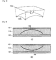
- Fig. 3 and Figs. 4(a) and 4(b) show the photovoltaic module when the insulating sheet 104 is not provided in the laminated structure shown in Fig. 1 .
- Fig. 3 is a conceptual diagram illustrating the deformed state of the photoelectric conversion element 103.
- a photoelectric conversion element 103b has a plate shape before the laminate process and the photoelectric conversion element 103a is deformed in a dome shape in which four corners are warped downward and a central portion protrudes upward in the laminate process.
- the photoelectric conversion element 103 contacts or approaches the protective member 101 or the reinforcing member 102.
- Figs. 4(a) and 4(b) are cross-sectional views illustrating the laminated structure of the photovoltaic module after the laminate process.
- the gap between the protective member 101 and the reinforcing member 102 is sealed as the insulating layer 114 by the sealing members 105 and 106.
- both ends of the photoelectric conversion element 103 which are warped to the lower surface approach the upper surface of the reinforcing member 102. Therefore, it is possible to prevent a reduction in the insulation resistance between both ends of the photoelectric conversion element 103 and the reinforcing member 102.
- Fig. 4(b) is a diagram illustrating the laminated structure when the four corners of the photoelectric conversion element 103 are warped to the upper surface and the central portion thereof protrudes toward the lower surface.
- the central portion of the photoelectric conversion element 103 protrudes downward to approach the reinforcing member 102 and both ends of the photoelectric conversion element 103 approach the upper protective member 101. Therefore, in this example, it is necessary to prevent a reduction in the insulation resistance between the protective member 101 and the photoelectric conversion element 103 and a reduction in the insulation resistance between the central portion of the photoelectric conversion element 103 and the reinforcing member 102.
- the photovoltaic module according to this embodiment is installed on, for example, the roof of the house and is used in the temperature range from room temperature to about 80°C under the actual conditions of use. Under these conditions of use, a portion of the sealing members 105 and 106 (insulating layer 114) is softened and the photoelectric conversion element 103 is likely to be deformed. Therefore, the photoelectric conversion element 103 having a plate shape immediately after manufacture is gradually deformed under the actual conditions of use of the photovoltaic module. As in the example shown in Fig.
- the photoelectric conversion element 103 is not necessarily uniformly deformed, and the deformation of the photoelectric conversion element 103 varies depending on, for example, the distribution of the residual stress of the substrate 107 of the photoelectric conversion element 103 or the shape of the substrate 107. Therefore, in this embodiment, the insulating sheets are arranged on the upper surface, which is the light incident surface of the photoelectric conversion element 103, and the lower surface, which is a surface opposite to the light incident surface, at the position where the amount of protrusion of the photoelectric conversion element 103 is large, if needed, thereby preventing a reduction in the insulation resistance of the photovoltaic module. Next, an example of the arrangement of the insulating sheets of the photovoltaic module will be described.
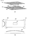
- Fig. 5(a) is a diagram schematically illustrating an example in which the insulating sheets 104 and 115 are provided on the upper surface and the lower surface of the photoelectric conversion element 103 in the photovoltaic module according to this embodiment. As shown in Fig.
- the insulating sheets 104 are arranged on the lower surface of the photoelectric conversion element 103 so as to cover both ends of the photoelectric conversion element 103 in the longitudinal direction, and the insulating sheet 115 is arranged on the upper surface of the photoelectric conversion element 103 at the center of the photoelectric conversion element 103.
- the insulating sheets 104 and 115 are arranged in this way, it is possible to prevent a reduction in the insulation resistance between the photoelectric conversion element 103, and the protective member 101 and the reinforcing member 102.
- Fig. 5(b) is a plan view schematically illustrating an example of the deformation of the photoelectric conversion element 103 and the arrangement of the insulating sheets 104 and 115.
- Fig. 5(b) shows only the photoelectric conversion element 103, the insulating sheet 115 provided on the upper surface of the photoelectric conversion element 103, and the insulating sheets 104 provided on the lower surface of the photoelectric conversion element 103, and does not show the other members.
- the vertical axis indicates the deformed state of the photoelectric conversion element 103 in the short-side direction and the vertical axis indicates the deformed state of the photoelectric conversion element 103 in the long-side direction. As shown in Fig.
- the central portion of the photoelectric conversion element 103 protrudes toward the uppermost side. Therefore, when the insulating sheet 104 is provided at the center of the upper surface of the photoelectric conversion element 103, it is possible to prevent a reduction in the insulation resistance between the protective member 101 and the photoelectric conversion element 103.
- the insulating sheet 115 provided on the light incident surface of the photoelectric conversion element 103 transmits at least light with a wavelength required to generate power from the photovoltaic device.
- the insulating sheet 115 may be made of any material capable of transmitting light.
- the insulating sheet 115 may be made of a colored material or a colorless material.
- Figs. 6(a) to 6(c) an example of the arrangement of the insulating sheets 104 on the lower surface of the photoelectric conversion element 103 will be described with reference to Figs. 6(a) to 6(c) .
- the insulating sheets 104 are arranged according to the warping of the photoelectric conversion element 103.
- Fig. 6(a) shows an example in which four rectangular insulating sheets 104 are arranged so as to cover four corners of the lower surface of the photoelectric conversion element 103. As shown in Fig.
- Fig. 6(a) when four corners of the photoelectric conversion element 103 are warped downward and the central portion thereof protrudes toward the upper surface, four corners of the lower surface protrude toward the lowermost side. Therefore, as shown in Fig. 6(a) , when the insulating sheets 104 are arranged so as to cover at least four corners of the photoelectric conversion element 103, it is possible to prevent a reduction in insulation resistance.
- Fig. 6(b) shows an example in which two rectangular insulating sheets 104 are arranged so as to cover both ends of the photoelectric conversion element 103 in the lateral direction.
- FIG. 6(c) shows an example in which one insulating sheet 104 is arranged so as to cover the entire lower surface of the photoelectric conversion element 103.
- the structure in which the insulating sheets 104 and 115 are arranged so as to cover the entire surface of the photoelectric conversion element 103 makes it possible to effectively prevent a reduction in insulation resistance.
- the insulating sheets 104 and 115 are arranged at positions including at least four corners in the direction in which four corners of the photoelectric conversion element 103 are warped.
- the width of the insulating sheet 104 provided at the end of the photoelectric conversion element 103 is not particularly limited as long as a reduction in the insulation resistance of the photoelectric conversion element 103 can be prevented.
- the width of the insulating sheet 104 may be about 2 cm. In this case, as shown in Fig.
- the insulating sheet 104 when the insulating sheet 104 is arranged so as to cover the entire lower surface of the photoelectric conversion element 103, the insulating sheet 104 having a long side with a length of more than 1 m is needed.
- the sum of the widths of the two insulating sheets 104 is about 4 cm, it is possible to prevent a reduction in insulation resistance using the insulating sheets 104 with an area that is equal to or less than 1/25 of the area of the insulating sheet 104 covering the entire lower surface of the photoelectric conversion element 103.
- the insulating sheet 104 since the insulating sheet 104 is arranged in at least a portion of the photoelectric conversion element 103 in which the amount of protrusion of the photoelectric conversion element 103 is large, it is possible to prevent a reduction in insulation resistance.
- Fig. 7(a) shows an example of the insulating sheets 115 when the amount of protrusion of the photoelectric conversion element 103 is substantially uniform in the short-side direction and the long-side direction of the photoelectric conversion element 103.
- the insulating sheets 115 having a rectangular shape in a plan view are arranged at the centers of four sides of the photoelectric conversion element 103. This arrangement makes it possible to prevent a reduction in the insulation resistance between the photoelectric conversion element 103 and the protective member 101.
- Fig. 7(b) shows an example of the arrangement of the insulating sheets 115 when the amount of protrusion of the photoelectric conversion element 103 is particularly large in the long-side direction.
- the insulating sheets 115 are arranged at the centers of the long sides of the photoelectric conversion element 103 where the amount of protrusion is large. This arrangement makes it possible to prevent a reduction in the insulation resistance between the photoelectric conversion element 103 and the protective member 101.
- Fig. 7(c) shows an example of the arrangement of the insulating sheets 115 when the amount of protrusion of the photoelectric conversion element 103 is particularly large in the short-side direction.
- the insulating sheets 115 are arranged at the centers of the short sides of the photoelectric conversion element 103 where the amount of protrusion is large. This arrangement makes it possible to prevent a reduction in the insulation resistance between the photoelectric conversion element 103 and the protective member 101.
- the insulating sheets 115 on the upper surface of the photoelectric conversion element 103 can be arranged at any positions on the upper surface and/or the lower surface of the photoelectric conversion element 103 according to the amount of protrusion of the photoelectric conversion element 103.
- the photoelectric conversion element 103 protrudes toward the upper surface.
- the photoelectric conversion element 103 protrudes toward the upper surface or the lower surface by the residual stress of the substrate 107. Therefore, when the insulating sheets 115 are arranged at any positions on the upper surface or the lower surface of the photoelectric conversion element 103, it is possible to prevent a reduction in the insulation resistance of the photoelectric conversion element 103.
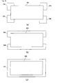
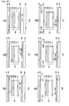
- Figs. 8(a) to 8(f) are diagrams schematically illustrating the laminated structure of the photovoltaic module and Figs. 9(a) to 9(f) are cross-sectional views illustrating the laminated structure of the photovoltaic module shown in Figs. 8(a) to 8(f) after the laminate process.
- the laminated structure shown in Figs. 8(a) to 8(f) corresponds to the cross-sectional views of Figs. 9(a) to 9(f) .
- Figs. 8(a) to 8(c) show an example in which the insulating sheets 104 are provided only on the lower surface opposite to the light incident surface of the photovoltaic module.
- the insulating sheets 104 are provided only at both ends of the lower surface of the photoelectric conversion element 103.
- the insulating sheets 104 are provided at both ends of the lower surface of the photoelectric conversion element 103, an adhesive member 116 is provided between the insulating sheet 104 and the photoelectric conversion element 103, and the sealing member 106 is provided between the insulating sheets 104 and the reinforcing member 102.
- Fig. 8(a) the insulating sheets 104 are provided only on the lower surface opposite to the light incident surface of the photovoltaic module.
- the insulating sheets 104 are provided only at both ends of the lower surface of the photoelectric conversion element 103.
- an adhesive member 116 is provided between the insulating sheet 104 and the photoelectric conversion element 103
- the sealing member 106 is provided between the insul
- the insulating sheets 104 are provided at both ends of the lower surface of the photoelectric conversion element 103, the sealing member 106 is provided between the insulating sheet 104 and the photoelectric conversion element 103, and the adhesive member 116 is provided between the insulating sheet 104 and the reinforcing member 102.
- the members are laminated in this way, it is possible to arbitrarily adjust the laminated structure between the photoelectric conversion element 103 and the reinforcing member 102, as shown in Figs. 9(a) to 9(c) .
- Figs. 8(d) to 8(f) show an example in which the insulating sheets 104 are provided on the lower surface of the photoelectric conversion element 103 and the insulating sheet 115 is provided on the upper surface of the light incident surface.
- the insulating sheet 115 is provided at the center of the upper surface of the photoelectric conversion element 103 and the insulating sheets 104 are provided at both ends of the lower surface of the photoelectric conversion element 103.
- the insulating sheet 115 is provided at the center of the upper surface of the photoelectric conversion element 103 and the sealing member 105 is provided between the insulating sheet 115 and the photoelectric conversion element 103.
- the insulating sheets 104 are provided at both ends of the lower surface of the photoelectric conversion element 103 and the sealing member 106 is provided between the insulating sheets 104 and the photoelectric conversion element 103.
- the insulating sheet 115 is provided at the center of the upper surface of the photoelectric conversion element 103
- the sealing member 105 is provided between the insulating sheet 115 and the protective member 101
- the adhesive member 116 is provided between the insulating sheet 115 and the photoelectric conversion element 103.
- the insulating sheets 104 are provided at both ends of the lower surface of the photoelectric conversion element 103 and the adhesive member 116 is provided between the insulating sheet 104 and the photoelectric conversion element 103.
- the sealing member 106 is provided between the insulating sheets 104 and the reinforcing member 102.
- the members are laminated in this way, it is possible to arbitrarily adjust the laminated structure between the photoelectric conversion element 103, and the protective member 101 and the reinforcing member 102, as shown in Figs. 9(d) to 9(f) .
- Figs. 10(a) to 10(f) are diagrams schematically illustrating the laminated structure of the photovoltaic module
- Figs. 11(a) to 11(f) are diagrams schematically illustrating the laminated structure of the photovoltaic module shown in Figs. 10(a) to 10(f) after the laminate process.
- the laminated structure shown in Figs. 10(a) to 10(f) corresponds to the cross-sectional views of Figs. 11(a) to 11(f) .
- Figs. 10(a) to 10(c) show an example in which the insulating sheet 104 is provided only on the lower surface opposite to the light incident surface of the photovoltaic module.
- the insulating sheet 104 is provided at the center of the lower surface of the photoelectric conversion element 103 and the sealing member 106 is provided between the insulating sheet 104 and the reinforcing member 102.
- the sealing member 106 is provided between the insulating sheet 104 and the reinforcing member 102.
- the insulating sheet 104 is provided at the center of the lower surface of the photoelectric conversion element 103, the sealing member 106 is provided between the insulating sheet 104 and the reinforcing member 102, and the adhesive member 116 is provided between the insulating sheet 104 and the photoelectric conversion element 103.
- the insulating sheet 104 is provided at the center of the lower surface of the photoelectric conversion element 103 and the sealing member 106 is provided between the insulating sheet 104 and the photoelectric conversion element 103.
- Figs. 10(d) to 10(f) show an example in which the insulating sheet 104 is provided on the lower surface of the photoelectric conversion element 103 and the insulating sheets 115 are provided on the upper surface which is the light incident surface.
- the insulating sheets 115 are provided at both ends of the upper surface of the photoelectric conversion element 103 and the sealing member 105 is provided between the insulating sheets 115 and the protective member 101.
- the sealing member 105 is provided between the insulating sheets 115 and the protective member 101.
- the insulating sheets 115 are provided at both ends of the upper surface of the photoelectric conversion element 103, the sealing member 105 is provided between the insulating sheets 115 and the protective member 101, and the adhesive member 116 is provided between the insulating sheet 115 and the photoelectric conversion element 103.
- the insulating sheets 115 are provided at both ends of the upper surface of the photoelectric conversion element 103, the sealing member 105 is provided between the insulating sheets 115 and the photoelectric conversion element 103, and the adhesive member 116 is provided between the insulating sheet 115 and the protective member 101.
- the arrangement positions of the insulating sheets 104 and 115 are not particularly limited in the range in which the insulation resistance of the photoelectric conversion element 103 can be prevented from being reduced, under the conditions of use of the photovoltaic module.
- the insulating sheet 115 provided on the upper surface, which is the sunlight incident surface, of the photoelectric conversion element 103 is made of a material capable of transmitting light with a wavelength required to generate power.
- the material forming the substrate 107 is not particularly limited.
- the substrate 107 may be various kinds of members, such as a stainless substrate and a resin film made of, for example, PET, PEN, polyamide, polyamideimide, polyimide, polycarbonate, PBT, PPS, liquid crystal polymer, or PEI.
- the substrate 107 it is preferable that the substrate 107 be made of polyimide with high insulation and heat resistance.
- the electrode 108 may be made of a general electrode material and the material forming the electrode 108 is not particularly limited.
- the material forming the transparent electrode 110 is not particularly limited.
- the electrode 108 is made of Ag and the transparent electrode 110 is made of ITO.
- the photoelectric conversion layer 109 may be made of any known material used in the photovoltaic module and the material forming the photoelectric conversion layer 109 is not particularly limited.
- the photoelectric conversion layer 109 may be made of amorphous silicon carbide (a-SiC), microcrystalline silicon ( ⁇ c-Si), ⁇ c-SiGe, ⁇ c-SiC, ⁇ c-Ge amorphous silicon (a-Si), and amorphous silicon germanium (a-SiGe).
- a-SiC amorphous silicon carbide
- ⁇ c-Si microcrystalline silicon
- ⁇ c-SiGe ⁇ c-SiGe
- a-Ge amorphous silicon germanium
- the sealing members 105 and 106 be made of a material that is stable against heat or water in terms of airtightly sealing the photoelectric conversion element 103. Since the sealing member 105 is provided on the light incident side of the photoelectric conversion element 103, it is preferable that the sealing member 105 be stable against light and be transparent. In addition, it is preferable that the sealing member 105 be made of a material that can be laminated in a short time, has high adhesion to the protective member 101 and the reinforcing member 102, and can follow the shape of the photovoltaic device. Further, the sealing member 105 may be made of a material capable of absorbing damage. In this case, for example, the photovoltaic module can be formed so as to be used even in an environment in which external force is applied.
- the sealing members 105 and 106 may be made of various kinds of resin materials that are likely to be softened and deformed by heating.
- the resin that is likely to be softened and deformed by heating may be a thermoplastic resin, a thermally crosslinkable resin, or a thermosetting resin.
- ethylene-vinyl acetate copolymer (EVA), polyvinyl butyral, silicon resin, ethylene-acrylate copolymer resin, ethylene-methacrylic acid resin, acrylic resin, polyethylene, or polypropylene may be used.
- the upper sealing member 105 and the lower sealing member 106 may be made of different materials.
- Each of the sealing members 105 and 106 is not a single resin layer, but may be a plurality of resin layers. When each of the sealing members 105 and 106 is a plurality of resin layers, it is possible to form a photovoltaic module that can be used even in an environment in which external force is applied.
- the protective member 101 may be made of any material capable of transmitting light, such as glass or a transparent resin.
- any material capable of transmitting light such as glass or a transparent resin.
- ETFE polyethylene tetrafluoro-ethylene
- PTFE polyethylene tetrafluoro-ethylene
- FEP FEP
- PFA polyethylene tetrafluoro-ethylene
- PVDF polyethylene tetrafluoro-ethylene
- PVF silicon resin with optical transparency, weather resistance, and light weight.
- FTFE is used.
- the insulating sheets 104 and 115 may be made of any material with rigidity and insulation higher than those of the sealing members 105 and 106 under the installed conditions for the use of the photovoltaic module and the manufacturing conditions of the photovoltaic module.
- the insulating sheets 104 and 115 may be made of various kinds of materials, such as a glass nonwoven and a fluorine-based film material. When the glass nonwoven is used, the members are laminated in the above-mentioned way. When the fluorine-based film material is used, slippage occurs between the film material and the sealing member or between the photoelectric conversion element 103 and the film material during lamination. Therefore, the insulating sheets are formed such that the slippage of the film material can be prevented.
- the insulating sheets 104 and 115 are made of a material with rigidity and an insulation property more than those of the sealing members 105 and 10. Therefore, it is possible to prevent a reduction in insulation resistance.
- the photovoltaic device may have various kinds of structures.
- various kinds of photovoltaic devices such as a photovoltaic device with a single structure, a photovoltaic device with a tandem structure, a photoelectric conversion element of a photovoltaic device with a three-layer tandem structure, a compound-based photovoltaic device, a dye-sensitized photovoltaic device, and an organic photovoltaic device, may be used.
- a substrate of a photoelectric conversion element was made of polyimide with a thickness of about 50 ⁇ m.
- An Ag electrode (thickness: 200 nm), two pin junctions (a-Si/a-SiGe tandem junctions, thickness: 800 nm) as a photoelectric conversion layer, an ITO film (thickness: 70 nm) as a transparent electrode were formed on the upper surface of the substrate.
- An Ag electrode (300 nm) was formed as a connection electrode on the lower surface of the substrate.
- a glass nonwoven with a thickness of 0.2 mm was used as an insulating sheet, and an EVA film having a thickness 0.3 mm and a width of 300 mm and an MFR (melt mass-flow rate) of 30 g/10 min was used as the upper and lower sealing members of the substrate.
- a fluorine-based film ETFE was used as a protective member.
- a steel plate coated with a polyester resin was used as a reinforcing member.
- the photoelectric conversion element had a width of 400 mm and a depth 200 of mm, the steel plate had a width of 450 mm and a depth of 300 mm, and the glass nonwoven had a depth of 220 mm, a width of 20 mm, and a thickness of 0.3 mm.
- the glass nonwoven was arranged at a position that was 10 mm away from the end of the EVA film in the longitudinal direction on the lower surface of the substrate.
- the electrodes at both ends of the photoelectric conversion element were connected to each other by a cable, and a voltage of 1000 V was applied between the connection portion and the steel plate. Then, the photovoltaic module was left in this state for 30 seconds until it become stable and the insulation resistance of the photovoltaic module was evaluated. Then, the high temperature/humidity test was performed under the conditions of a temperature of 85°C and a humidity of 95% for 3000 hours and the insulation property was evaluated. The evaluation result is shown in Table 1. The insulation property was good both before and after the high temperature/humidity test.
- a photoelectric conversion element, a sealing member, and a protective member were formed by the same method as that in Example 1.
- An insulating sheet provided between the photoelectric conversion element and the protective member was made of ETFE with a thickness of 25 ⁇ m.
- the insulating sheet was arranged between the photoelectric conversion element and the sealing member such that the center of the insulating sheet in the lateral direction (width direction) was aligned with both ends of a light incident surface of the photoelectric conversion element in the longitudinal direction (width direction).
- a sealing member that was made of EVA with a thickness of 0.3 mm was provided between the insulating sheet and the photoelectric conversion element.
- the laminate process was performed under the same conditions as those in Example 1.
- Insulation resistance was evaluated by the same method as that in Example 1. The evaluation result is shown in Table 1. Similar to Example 1, a good insulation property was obtained before and after the high temperature/humidity test.
- a photoelectric conversion element, a sealing member, and a protective member were formed by the same method as that in Example 1.
- An insulating sheet provided between the photoelectric conversion element and the protective member was made of ETFE with a thickness of 25 ⁇ m.
- the insulating sheet was arranged between an EVA film formed on a surface opposite to a light incident surface of the photoelectric conversion element and a steel plate such that the center of the insulating sheet in the lateral direction (width direction) was aligned with both ends of the surface opposite to light incident surface of the photoelectric conversion element in the longitudinal direction (width direction).
- a modified silicon adhesive was used between the insulating sheet and the steel plate. The laminate process was performed under the same conditions as those in Example 1.
- Insulation resistance was evaluated by the same method as that in Example 1. The evaluation result is shown in Table 1. Similar to Examples 1 and 2, a good insulation property was obtained before and after the high temperature/humidity test.
- a photoelectric conversion element, a sealing member, and a protective member were formed by the same method as that in Example 1, but no insulating sheet was provided between the photoelectric conversion element and the sealing member.
- the laminate process was performed under the same conditions as those in Example 1.
- Insulation resistance was evaluated by the same method as that in Example 1. The evaluation result is shown in Table 1. Before and after the high temperature/humidity test, the insulation resistance was low and did not reach a target value.
- a photoelectric conversion element, a sealing member, and a protective member were formed by the same method as that in Example 1, and an insulating sheet (having a width of 400 mm and a depth of 200 mm) made of a glass nonwoven was provided between the entire surfaces of the photoelectric conversion element and the sealing member.
- the laminate process was performed under the same conditions as those in Example 1.
- Insulation resistance was evaluated by the same method as that in Example 1. The evaluation result is shown in Table 2. Before the high temperature/humidity test after manufacture, target insulation resistance was obtained, similar to Example 1, but the insulation resistance was reduced after the high temperature/humidity test.
- Example 1 Example 2
- Example 3 Comparative example 1 Comparative example 2 After manufacture (before high temperature/humidity test)
- ⁇ ⁇ ⁇ ⁇ ⁇ ⁇ ⁇ ⁇ After high temperature/humidity test
- ⁇ ⁇ ⁇ ⁇ ⁇ ⁇ Measurement result of insulation resistance ⁇ : 1 ⁇ 10 5 M ⁇ or more at 1000 V, ⁇ : less than 1 ⁇ 10 5 M ⁇ at 1000 V
- the invention is not limited to the above-described embodiments, but various modifications and changes of the invention can be made.
- the numerical values, dimensions, and materials according to the above-described embodiments are not particularly limited.
- the thickness of the EVA film in Examples 1 to 3 is not limited to 0.3 mm, but may be in the range of about 0.1 mm to 2 mm.
- Various modifications and changes of the invention can be made without departing from the scope and spirit of the invention.
- the invention can be applied to, for example, an outdoor photovoltaic module or a thin-film photovoltaic device.
Landscapes
- Engineering & Computer Science (AREA)
- Architecture (AREA)
- Civil Engineering (AREA)
- Structural Engineering (AREA)
- Physics & Mathematics (AREA)
- Condensed Matter Physics & Semiconductors (AREA)
- Electromagnetism (AREA)
- General Physics & Mathematics (AREA)
- Computer Hardware Design (AREA)
- Microelectronics & Electronic Packaging (AREA)
- Power Engineering (AREA)
- Photovoltaic Devices (AREA)
Applications Claiming Priority (2)
| Application Number | Priority Date | Filing Date | Title |
|---|---|---|---|
| JP2008327954 | 2008-12-24 | ||
| PCT/JP2009/070832 WO2010073932A1 (ja) | 2008-12-24 | 2009-12-14 | 太陽電池モジュール |
Publications (2)
| Publication Number | Publication Date |
|---|---|
| EP2383796A1 true EP2383796A1 (de) | 2011-11-02 |
| EP2383796A4 EP2383796A4 (de) | 2012-12-19 |
Family
ID=42287548
Family Applications (1)
| Application Number | Title | Priority Date | Filing Date |
|---|---|---|---|
| EP09834735A Withdrawn EP2383796A4 (de) | 2008-12-24 | 2009-12-14 | Solarzellenmodul |
Country Status (5)
| Country | Link |
|---|---|
| US (1) | US20110315187A1 (de) |
| EP (1) | EP2383796A4 (de) |
| JP (1) | JPWO2010073932A1 (de) |
| CN (1) | CN102265409A (de) |
| WO (1) | WO2010073932A1 (de) |
Cited By (1)
| Publication number | Priority date | Publication date | Assignee | Title |
|---|---|---|---|---|
| GB2570493A (en) * | 2018-01-29 | 2019-07-31 | Sunew Filmes Fotovoltaicos | Solar panel arrangement |
Families Citing this family (1)
| Publication number | Priority date | Publication date | Assignee | Title |
|---|---|---|---|---|
| WO2015045231A1 (ja) * | 2013-09-30 | 2015-04-02 | パナソニックIpマネジメント株式会社 | 光電変換装置および当該装置に使用される光電変換ユニット |
Citations (3)
| Publication number | Priority date | Publication date | Assignee | Title |
|---|---|---|---|---|
| EP0680097A2 (de) * | 1994-04-28 | 1995-11-02 | Canon Kabushiki Kaisha | Sonnenzellenmodul mit einer Schutzoberfläche bestehend aus einem ein Ultraviolettabsorbierungsmittel enthaltenden Fluorharz |
| EP1172864A1 (de) * | 2000-07-11 | 2002-01-16 | SANYO ELECTRIC Co., Ltd. | Solarzellenmodul |
| EP1840974A2 (de) * | 2006-03-30 | 2007-10-03 | Sanyo Electric Co., Ltd. | Fotovoltaisches Modul und Herstellungsverfahren dafür |
Family Cites Families (7)
| Publication number | Priority date | Publication date | Assignee | Title |
|---|---|---|---|---|
| JPH1056191A (ja) * | 1996-08-08 | 1998-02-24 | Canon Inc | 太陽電池モジュール |
| JP3825843B2 (ja) * | 1996-09-12 | 2006-09-27 | キヤノン株式会社 | 太陽電池モジュール |
| JP2000345675A (ja) * | 1999-03-26 | 2000-12-12 | Canon Inc | 太陽電池モジュール、太陽電池付き屋根、及び太陽電池発電システム |
| DE10023546C2 (de) * | 2000-05-15 | 2002-11-07 | Webasto Vehicle Sys Int Gmbh | Solardeckel |
| EP1614165A2 (de) * | 2003-04-16 | 2006-01-11 | Apollon Solar | Fotovoltaisches modul und herstellungsverfahren dafür |
| JP4401158B2 (ja) * | 2003-12-16 | 2010-01-20 | シャープ株式会社 | 太陽電池の製造方法 |
| ITMI20040253A1 (it) * | 2004-02-16 | 2004-05-16 | Curvet S P A | Modulo fotovoltaico curvo processo produttivo e relativa vetrara isolante termicamente ed acusticamente |
-
2009
- 2009-12-14 US US13/142,275 patent/US20110315187A1/en not_active Abandoned
- 2009-12-14 JP JP2010544011A patent/JPWO2010073932A1/ja active Pending
- 2009-12-14 WO PCT/JP2009/070832 patent/WO2010073932A1/ja active Application Filing
- 2009-12-14 CN CN200980152718.XA patent/CN102265409A/zh active Pending
- 2009-12-14 EP EP09834735A patent/EP2383796A4/de not_active Withdrawn
Patent Citations (3)
| Publication number | Priority date | Publication date | Assignee | Title |
|---|---|---|---|---|
| EP0680097A2 (de) * | 1994-04-28 | 1995-11-02 | Canon Kabushiki Kaisha | Sonnenzellenmodul mit einer Schutzoberfläche bestehend aus einem ein Ultraviolettabsorbierungsmittel enthaltenden Fluorharz |
| EP1172864A1 (de) * | 2000-07-11 | 2002-01-16 | SANYO ELECTRIC Co., Ltd. | Solarzellenmodul |
| EP1840974A2 (de) * | 2006-03-30 | 2007-10-03 | Sanyo Electric Co., Ltd. | Fotovoltaisches Modul und Herstellungsverfahren dafür |
Non-Patent Citations (1)
| Title |
|---|
| See also references of WO2010073932A1 * |
Cited By (1)
| Publication number | Priority date | Publication date | Assignee | Title |
|---|---|---|---|---|
| GB2570493A (en) * | 2018-01-29 | 2019-07-31 | Sunew Filmes Fotovoltaicos | Solar panel arrangement |
Also Published As
| Publication number | Publication date |
|---|---|
| EP2383796A4 (de) | 2012-12-19 |
| CN102265409A (zh) | 2011-11-30 |
| WO2010073932A1 (ja) | 2010-07-01 |
| JPWO2010073932A1 (ja) | 2012-06-14 |
| US20110315187A1 (en) | 2011-12-29 |
Similar Documents
| Publication | Publication Date | Title |
|---|---|---|
| US6307145B1 (en) | Solar cell module | |
| US6515216B2 (en) | Photovoltaic device assembly, solar cell module using the same and manufacture method of solar cell module | |
| KR100325955B1 (ko) | 태양전지모듈및태양전지모듈용보강부재 | |
| KR100376896B1 (ko) | 광기전력소자 | |
| EP0874404B1 (de) | Solarzellenmodul und Verfahren zu dessen Herstellung | |
| US20060207645A1 (en) | Method of manufacturing a solor cell module | |
| US20090272436A1 (en) | Non-glass photovoltaic module and methods for manufacture | |
| EP1921684A1 (de) | Solarzellenmodul und herstellungsverfahren dafür | |
| JP2004319800A (ja) | 太陽電池モジュール | |
| EP2780948A1 (de) | Neue solarmodule, trägerschichtstapel und herstellungsverfahren dafür | |
| US20120325315A1 (en) | Photoelectric converter device and method for its manufacture | |
| US20140137939A1 (en) | Solar-cell module and manufacturing method therefor | |
| KR20110021934A (ko) | 광기전성 유리 적층 물품 및 층 물품 | |
| US20240178334A1 (en) | Method for manufacturing photovoltaic module and photovoltaic module | |
| US20180122972A1 (en) | Semi-flexible solar module using crystaline solar cells and method for fabrication thereof | |
| JP5304955B1 (ja) | 融雪機能付き太陽電池モジュール | |
| JP2012204458A (ja) | 太陽電池モジュールの製造方法 | |
| EP2383796A1 (de) | Solarzellenmodul | |
| JP2006295145A (ja) | 太陽電池モジュールの製造方法 | |
| JP2006278702A (ja) | 太陽電池モジュール及びその製造方法 | |
| JP2013030734A (ja) | 太陽電池モジュール | |
| JP5598986B2 (ja) | 太陽電池モジュール | |
| JP2007311651A (ja) | 真空ラミネート装置および真空ラミネート方法 | |
| JPH11214734A (ja) | 太陽電池モジュールおよびその製造方法およびその施工方法および太陽電池発電システム | |
| KR101477499B1 (ko) | 경량 태양광 모듈 및 그 제조방법 |
Legal Events
| Date | Code | Title | Description |
|---|---|---|---|
| PUAI | Public reference made under article 153(3) epc to a published international application that has entered the european phase |
Free format text: ORIGINAL CODE: 0009012 |
|
| 17P | Request for examination filed |
Effective date: 20110725 |
|
| AK | Designated contracting states |
Kind code of ref document: A1 Designated state(s): AT BE BG CH CY CZ DE DK EE ES FI FR GB GR HR HU IE IS IT LI LT LU LV MC MK MT NL NO PL PT RO SE SI SK SM TR |
|
| DAX | Request for extension of the european patent (deleted) | ||
| A4 | Supplementary search report drawn up and despatched |
Effective date: 20121119 |
|
| RIC1 | Information provided on ipc code assigned before grant |
Ipc: H01L 31/042 20060101AFI20121113BHEP Ipc: H01L 31/048 20060101ALI20121113BHEP |
|
| STAA | Information on the status of an ep patent application or granted ep patent |
Free format text: STATUS: THE APPLICATION IS DEEMED TO BE WITHDRAWN |
|
| 18D | Application deemed to be withdrawn |
Effective date: 20130618 |