EP2383113A1 - Metal foil with carrier - Google Patents
Metal foil with carrier Download PDFInfo
- Publication number
- EP2383113A1 EP2383113A1 EP09834550A EP09834550A EP2383113A1 EP 2383113 A1 EP2383113 A1 EP 2383113A1 EP 09834550 A EP09834550 A EP 09834550A EP 09834550 A EP09834550 A EP 09834550A EP 2383113 A1 EP2383113 A1 EP 2383113A1
- Authority
- EP
- European Patent Office
- Prior art keywords
- carrier
- metal foil
- foil
- copper
- copper foil
- Prior art date
- Legal status (The legal status is an assumption and is not a legal conclusion. Google has not performed a legal analysis and makes no representation as to the accuracy of the status listed.)
- Granted
Links
Images
Classifications
-
- H—ELECTRICITY
- H05—ELECTRIC TECHNIQUES NOT OTHERWISE PROVIDED FOR
- H05K—PRINTED CIRCUITS; CASINGS OR CONSTRUCTIONAL DETAILS OF ELECTRIC APPARATUS; MANUFACTURE OF ASSEMBLAGES OF ELECTRICAL COMPONENTS
- H05K3/00—Apparatus or processes for manufacturing printed circuits
- H05K3/02—Apparatus or processes for manufacturing printed circuits in which the conductive material is applied to the surface of the insulating support and is thereafter removed from such areas of the surface which are not intended for current conducting or shielding
- H05K3/022—Processes for manufacturing precursors of printed circuits, i.e. copper-clad substrates
- H05K3/025—Processes for manufacturing precursors of printed circuits, i.e. copper-clad substrates by transfer of thin metal foil formed on a temporary carrier, e.g. peel-apart copper
-
- H—ELECTRICITY
- H05—ELECTRIC TECHNIQUES NOT OTHERWISE PROVIDED FOR
- H05K—PRINTED CIRCUITS; CASINGS OR CONSTRUCTIONAL DETAILS OF ELECTRIC APPARATUS; MANUFACTURE OF ASSEMBLAGES OF ELECTRICAL COMPONENTS
- H05K1/00—Printed circuits
- H05K1/02—Details
- H05K1/09—Use of materials for the conductive, e.g. metallic pattern
-
- B—PERFORMING OPERATIONS; TRANSPORTING
- B32—LAYERED PRODUCTS
- B32B—LAYERED PRODUCTS, i.e. PRODUCTS BUILT-UP OF STRATA OF FLAT OR NON-FLAT, e.g. CELLULAR OR HONEYCOMB, FORM
- B32B15/00—Layered products comprising a layer of metal
- B32B15/04—Layered products comprising a layer of metal comprising metal as the main or only constituent of a layer, which is next to another layer of the same or of a different material
- B32B15/08—Layered products comprising a layer of metal comprising metal as the main or only constituent of a layer, which is next to another layer of the same or of a different material of synthetic resin
-
- B—PERFORMING OPERATIONS; TRANSPORTING
- B32—LAYERED PRODUCTS
- B32B—LAYERED PRODUCTS, i.e. PRODUCTS BUILT-UP OF STRATA OF FLAT OR NON-FLAT, e.g. CELLULAR OR HONEYCOMB, FORM
- B32B15/00—Layered products comprising a layer of metal
- B32B15/20—Layered products comprising a layer of metal comprising aluminium or copper
-
- H—ELECTRICITY
- H05—ELECTRIC TECHNIQUES NOT OTHERWISE PROVIDED FOR
- H05K—PRINTED CIRCUITS; CASINGS OR CONSTRUCTIONAL DETAILS OF ELECTRIC APPARATUS; MANUFACTURE OF ASSEMBLAGES OF ELECTRICAL COMPONENTS
- H05K2201/00—Indexing scheme relating to printed circuits covered by H05K1/00
- H05K2201/10—Details of components or other objects attached to or integrated in a printed circuit board
- H05K2201/10227—Other objects, e.g. metallic pieces
-
- H—ELECTRICITY
- H05—ELECTRIC TECHNIQUES NOT OTHERWISE PROVIDED FOR
- H05K—PRINTED CIRCUITS; CASINGS OR CONSTRUCTIONAL DETAILS OF ELECTRIC APPARATUS; MANUFACTURE OF ASSEMBLAGES OF ELECTRICAL COMPONENTS
- H05K2203/00—Indexing scheme relating to apparatus or processes for manufacturing printed circuits covered by H05K3/00
- H05K2203/01—Tools for processing; Objects used during processing
- H05K2203/0147—Carriers and holders
- H05K2203/0152—Temporary metallic carrier, e.g. for transferring material
-
- H—ELECTRICITY
- H05—ELECTRIC TECHNIQUES NOT OTHERWISE PROVIDED FOR
- H05K—PRINTED CIRCUITS; CASINGS OR CONSTRUCTIONAL DETAILS OF ELECTRIC APPARATUS; MANUFACTURE OF ASSEMBLAGES OF ELECTRICAL COMPONENTS
- H05K2203/00—Indexing scheme relating to apparatus or processes for manufacturing printed circuits covered by H05K3/00
- H05K2203/02—Details related to mechanical or acoustic processing, e.g. drilling, punching, cutting, using ultrasound
- H05K2203/0285—Using ultrasound, e.g. for cleaning, soldering or wet treatment
-
- H—ELECTRICITY
- H05—ELECTRIC TECHNIQUES NOT OTHERWISE PROVIDED FOR
- H05K—PRINTED CIRCUITS; CASINGS OR CONSTRUCTIONAL DETAILS OF ELECTRIC APPARATUS; MANUFACTURE OF ASSEMBLAGES OF ELECTRICAL COMPONENTS
- H05K3/00—Apparatus or processes for manufacturing printed circuits
- H05K3/46—Manufacturing multilayer circuits
- H05K3/4644—Manufacturing multilayer circuits by building the multilayer layer by layer, i.e. build-up multilayer circuits
- H05K3/4652—Adding a circuit layer by laminating a metal foil or a preformed metal foil pattern
-
- Y—GENERAL TAGGING OF NEW TECHNOLOGICAL DEVELOPMENTS; GENERAL TAGGING OF CROSS-SECTIONAL TECHNOLOGIES SPANNING OVER SEVERAL SECTIONS OF THE IPC; TECHNICAL SUBJECTS COVERED BY FORMER USPC CROSS-REFERENCE ART COLLECTIONS [XRACs] AND DIGESTS
- Y10—TECHNICAL SUBJECTS COVERED BY FORMER USPC
- Y10T—TECHNICAL SUBJECTS COVERED BY FORMER US CLASSIFICATION
- Y10T428/00—Stock material or miscellaneous articles
- Y10T428/12—All metal or with adjacent metals
- Y10T428/12472—Microscopic interfacial wave or roughness
-
- Y—GENERAL TAGGING OF NEW TECHNOLOGICAL DEVELOPMENTS; GENERAL TAGGING OF CROSS-SECTIONAL TECHNOLOGIES SPANNING OVER SEVERAL SECTIONS OF THE IPC; TECHNICAL SUBJECTS COVERED BY FORMER USPC CROSS-REFERENCE ART COLLECTIONS [XRACs] AND DIGESTS
- Y10—TECHNICAL SUBJECTS COVERED BY FORMER USPC
- Y10T—TECHNICAL SUBJECTS COVERED BY FORMER US CLASSIFICATION
- Y10T428/00—Stock material or miscellaneous articles
- Y10T428/12—All metal or with adjacent metals
- Y10T428/12493—Composite; i.e., plural, adjacent, spatially distinct metal components [e.g., layers, joint, etc.]
- Y10T428/12736—Al-base component
-
- Y—GENERAL TAGGING OF NEW TECHNOLOGICAL DEVELOPMENTS; GENERAL TAGGING OF CROSS-SECTIONAL TECHNOLOGIES SPANNING OVER SEVERAL SECTIONS OF THE IPC; TECHNICAL SUBJECTS COVERED BY FORMER USPC CROSS-REFERENCE ART COLLECTIONS [XRACs] AND DIGESTS
- Y10—TECHNICAL SUBJECTS COVERED BY FORMER USPC
- Y10T—TECHNICAL SUBJECTS COVERED BY FORMER US CLASSIFICATION
- Y10T428/00—Stock material or miscellaneous articles
- Y10T428/12—All metal or with adjacent metals
- Y10T428/12493—Composite; i.e., plural, adjacent, spatially distinct metal components [e.g., layers, joint, etc.]
- Y10T428/12736—Al-base component
- Y10T428/1275—Next to Group VIII or IB metal-base component
-
- Y—GENERAL TAGGING OF NEW TECHNOLOGICAL DEVELOPMENTS; GENERAL TAGGING OF CROSS-SECTIONAL TECHNOLOGIES SPANNING OVER SEVERAL SECTIONS OF THE IPC; TECHNICAL SUBJECTS COVERED BY FORMER USPC CROSS-REFERENCE ART COLLECTIONS [XRACs] AND DIGESTS
- Y10—TECHNICAL SUBJECTS COVERED BY FORMER USPC
- Y10T—TECHNICAL SUBJECTS COVERED BY FORMER US CLASSIFICATION
- Y10T428/00—Stock material or miscellaneous articles
- Y10T428/12—All metal or with adjacent metals
- Y10T428/12493—Composite; i.e., plural, adjacent, spatially distinct metal components [e.g., layers, joint, etc.]
- Y10T428/12771—Transition metal-base component
- Y10T428/12861—Group VIII or IB metal-base component
- Y10T428/12903—Cu-base component
-
- Y—GENERAL TAGGING OF NEW TECHNOLOGICAL DEVELOPMENTS; GENERAL TAGGING OF CROSS-SECTIONAL TECHNOLOGIES SPANNING OVER SEVERAL SECTIONS OF THE IPC; TECHNICAL SUBJECTS COVERED BY FORMER USPC CROSS-REFERENCE ART COLLECTIONS [XRACs] AND DIGESTS
- Y10—TECHNICAL SUBJECTS COVERED BY FORMER USPC
- Y10T—TECHNICAL SUBJECTS COVERED BY FORMER US CLASSIFICATION
- Y10T428/00—Stock material or miscellaneous articles
- Y10T428/12—All metal or with adjacent metals
- Y10T428/12493—Composite; i.e., plural, adjacent, spatially distinct metal components [e.g., layers, joint, etc.]
- Y10T428/12771—Transition metal-base component
- Y10T428/12861—Group VIII or IB metal-base component
- Y10T428/12903—Cu-base component
- Y10T428/1291—Next to Co-, Cu-, or Ni-base component
Definitions
- the present invention relates to a copper foil with a carrier used in producing a single-sided or multilayer laminated plate of two or more layers for use in a print wiring board.
- a typical example of a multilayer laminated body is a printed circuit board.
- a printed circuit board is basically configured from a dielectric material referred to as a "prepreg" that is obtained by impregnating synthetic resin in a base material such as a synthetic resin plate, glass plate, nonwoven glass fabric or paper.
- a sheet such as a copper or copper alloy foil having electrical conductivity is bonded to the prepreg surface, both of the front and back surfaces.
- a laminate that is assembled as described above is generally referred to as a CCL, namely, a Copper Clad Laminate material.
- a multilayer board When copper foils are multi-layered on the CCL material with use of the prepreg, this is referred to as a multilayer board.
- Other foils made of aluminum, nickel, zinc or the like may also be used in substitute for the copper or copper alloy foil.
- the foil thickness is roughly 5 to 200 ⁇ m.
- a copper foil with a carrier is used for the purpose of preventing the adhesion of foreign matter on the surface of the copper foil and for the purpose of improving the handling ability.
- a stainless pressing plate called "mirror plate” having a flat pressing surface with a thickness of 0.2 to 2 mm so that the M surface is on top ('M surface' as used herein represents 'rough surface', and both of the expressions are used interchangeably hereinafter), subsequently a prescribed number of prepregs, subsequently a printed circuit board in which a circuit is formed on a CCL material referred to as the inner layer core, subsequently a prepreg, and subsequently an ultrathin copper foil to which a carrier is peelably bonded are mounted so that the M surface is at the bottom, and by laminating
- lamination assembly operation upon performing the lay-up operation, lamination assembly operation, in other words, the worker needs to alternatively repeat the process of lamination so that the M surface of the copper foil is on top or the M surface is at the bottom, and there is a problem in that the work efficiency will deteriorate.
- the copper foil and the carrier are of the same size, it is difficult to peel one copper foil at a time during the lay-up, which is also a problem in that the workability deteriorates on this point.
- an aluminum plate JIS#5182
- the linear expansion coefficient of the aluminum plate is 23.8 ⁇ 10 -6 /°C and great compared to 16.5 ⁇ 10 -6 /°C of the copper foil as the constituent material of the substrate and the polymerized prepreg (C stage: 12 to 18 ⁇ 10 -6 /°C)
- C stage: 12 to 18 ⁇ 10 -6 /°C the polymerized prepreg
- the linear expansion coefficient at normal temperature of the various materials used in the print wiring board is as follows. It is evident that the linear expansion coefficient of the aluminum plate is fairly greater than the other materials.
- the present invention was devised in view of the foregoing circumstances, and relates to a copper foil with a carrier that is used in producing a single-sided or multilayer laminated body of two or more layers for use in a print wiring board, and particularly relates to a copper foil with a carrier to be used upon producing a laminated plate.
- an object of this invention is to realize improvement in the handling ability in the production process of a printed board and cost reduction based on an improved production yield.
- the present invention provides:
- the present invention additionally provides:
- the present invention further provides:
- the first feature of the metal foil with a carrier of the present invention is that it is a laminated body in which a carrier A and a metal foil B are placed alternately, wherein the metal foil with a carrier comprises a structure where the adjoining carrier A has an area which covers the entire surface of the metal foil B, and the edge of the carrier A protrudes partially or entirely from the metal foil B. Accordingly, it is therefore easy to differentiate a laminated pair of the carrier A and the metal foil B from a similar type of laminated pair of the carrier A and the metal foil B, and the worker's handling performance will improve. Moreover, even upon peeling the carrier from the copper foil, peeling is easy since there is a part (edge or end) which differs in dimension.
- the work efficiency will improve dramatically since the worker no longer needs to perform operations of placing the M surface of the copper foil on bottom or top.
- the glossy surface or rough surface or the carrier or the glossy surface or the rough surface of the copper foil can be arbitrarily used for different purposes.
- the use of a copper foil as the carrier is optional, if the carrier is made of copper foil, the linear expansion coefficient will be of the same level as the copper foil as the constituent material of the substrate and the polymerized prepreg, and, since the misalignment of the circuit will not occur, this invention yields a superior effect of minimizing defective goods and thereby improving the production yield.
- the second feature of the copper foil with a carrier of the present invention is that it has a structure where the glossy surface of the metal foil B is subject to ultrasonic bonding so as to come in contact with the carrier A made of aluminum or copper or copper alloy.
- the peeling of the aluminum layer after lamination is facilitated, and an effect is yielded in that it is possible to prevent the peeled copper foil from breaking and the aluminum carrier from remaining on the copper foil.
- the carrier A is a rolled copper foil or an electrolytic copper foil
- the glossy surface of the copper foil B is subject to ultrasonic bonding so as to come in contact with the roughened surface of the rolled copper foil or the rough surface or the roughened surface of the electrolytic copper foil.
- the peelability upon separating the bond can be improved. Accordingly, an effect is yielded in that these can be arbitrarily combined and used.
- a printed circuit board is basically configured from a dielectric material referred to as a "prepreg" that is obtained by impregnating synthetic resin in a base material such as a synthetic resin plate, glass plate, nonwoven glass fabric or paper.
- a sheet such as a copper or copper alloy foil having electrical conductivity is bonded with the prepreg in-between.
- a laminate that is assembled as described above is generally referred to as a CCL, namely, Copper Clad Laminate material.
- CCL Copper Clad Laminate material.
- other foils made of aluminum, nickel, zinc or the like are sometimes used.
- the foil thickness is roughly 5 to 200 ⁇ m.
- the metal foil with a carrier of the present invention is shown in Fig. 1 .
- the carrier is shown as A and the metal foil is shown as B.
- the carrier A and the metal foil B are separated eventually, they can be easily peeled mechanically.
- the CCL material cannot be peeled, the structure and function thereof are completely different from the present invention.
- the carrier A is larger than the area of the metal foil B, and the case of Fig. 1 (a) shows a structure where two opposing sides protrude farther than the metal foil B, and the case of Fig.
- 1 (b) shows a structure where one side is protruding farther than the metal foil B.
- the amount of protrusion can be suitably selected according to the workability, entirely as one thinks proper. This range is approximately 1 cm to 10 cm; however, it goes without saying that the protrusion may be prepared beyond the foregoing range.
- the remaining sides of the carrier A are desirably aligned with the metal foil B, this may be arbitrarily adjusted or selected according to the objective of the production process.
- the primary object of the present invention is to improve the handling performance of workers as a whole by realizing a structure where the carrier A protrudes from the metal foil B by enlarging the area of the carrier A to be greater than the metal foil B, facilitating the differentiation of a laminated pair of the carrier A and the metal foil B from a similar type of laminated pair of the carrier A and the metal foil B, and facilitating the peeling process by providing a part (edge or end) which differs in dimension upon peeling the carrier A from the metal foil B.
- the carrier A and the metal foil B are formed in a quadrilateral, namely, a rectangular or a square. Although this shape is selectable so as long as it is convenient in the handling during its manufacture, a square or a rectangular is generally used.
- one side of the carrier A and one side of the metal foil B are mutually aligned, or two adjoining sides or two opposing sides of the carrier A and the metal foil B are mutually aligned.
- the foregoing selection is also optional.
- the carrier-attached metal foil of the present invention a preferred mode is the metal foil B being a copper foil or a copper alloy foil, and the carrier A being a copper foil or a copper alloy foil.
- the carrier-attached metal foil of the present invention yields numerous advantages as a result of the carrier A and the metal foil B respectively having a glossy surface, and the respective glossy surfaces being laminated to face each other, and this is also a preferred mode of lamination.
- Fig. 2 shows a metal foil with a carrier with a structure where the carrier A protrudes from the metal foil B by enlarging the carrier A to have a greater area than the metal foil B, and the respective glossy surfaces are laminated to face each other.
- the upper metal foil B has an upper surface using a copper foil as the M surface and a lower surface as the S surface
- the lower carrier A has an upper surface as the S surface and the lower surface as the M surface, and the S surfaces thereof are mutually bonded.
- the carrier A and the metal foil B are foils made of the same material, the respective front and back glossy surfaces of the carrier A and the metal foil B after peeling can be used without having to perform any reversing operations.
- This enables the considerable improvement in workability.
- Conventionally when a worker had to place the M surface of the copper foil on top and place the M surface on bottom in the layup (lamination) process and alternately repeat this process, there was a problem in that the work efficiency would deteriorate, but the present invention yields an effect of resolving the problem at once.
- the present invention since the present invention has a structure where the carrier A protrudes from the metal foil B by enlarging the area of the carrier A to be greater than the metal foil B, it is possible to facilitate the differentiation of a laminated pair of the carrier A and the metal foil B from a similar type of laminated pair of the carrier A and the metal foil B, and facilitate the peeling process by providing a part (edge or end) which differs in dimension upon peeling the carrier A from the metal foil B.
- the present invention yields an effect of considerably improving the handling performance of workers compared to conventional processes, and the prominence of the present invention is evident.
- the carrier A and the metal foil B are mutually bonded to avoid misalignment, and these are desirably bonded by way of an adhesive, caulking, bi-fold or welding.
- the bonding method is also selectable, but the foregoing bonding methods are preferred.
- Fig. 3 shows an example where the glossy surface of the carrier (for example, copper foil) A is placed on top and the glossy surface of the metal (copper) foil B is placed on bottom and welded based on ultrasonic welding.
- a part of the glossy surface of the carrier (for example, copper foil) A is exposed on the right side.
- the rough surface of the metal (copper) foil B can be seen as the back side. Since the carrier A and the metal foil B are fixed as described, the worker's layup (lamination) process is effectively improved. Moreover, since the surface is not fixed entirely, the peeling, or scaling process after lamination is also facilitated.
- a copper foil or a copper alloy foil is a typical example and most favorable, but foils of aluminum, nickel, zinc and the like may also be used.
- a foil of the same material as the metal foil B can be used as the carrier A.
- an electrolytic foil or a rolled foil with a thickness of 5 to 120 ⁇ m can be used.
- the coefficient of thermal expansion of the metal foil B is desirably within the range of +10% and -30% of the coefficient of thermal expansion of the metal foil B. Consequently, it is possible to effectively prevent the misalignment of the circuit caused by the difference in thermal expansion, and thereby minimize defective goods and improve the production yield.
- the carrier A and the metal foil B are usually mechanically peeled before the process of plating or etching or the like, the peel strength thereof is desirably 1 g/cm or more and 1 kg/cm or less.
- the peeling surface is desirably the boundary of the carrier A and the metal foil B. The residue of other material will require a removal work thereof and cause the overall process to become complicated, and must be avoided.
- a prepreg prepared from epoxy resin was used as the resin material.
- An intended number of prepregs were laminated on the metal foil with a carrier, a two-layer printed circuit board referred to as an inner layer core was subsequently laminated thereon, a prepreg was subsequently laminated thereon, and a metal foil with a carrier was further formed thereon, in the foregoing order, in order to complete one set of a four-layer substrate material assembly unit. Subsequently, this unit called "page” was repeatedly laminated about 10 times to configure a press assembly called "book”.
- the present invention is unique with respect to the structure of the metal foil with a carrier, and comprises a structure where the carrier A protrudes from the metal foil B.
- Fig. 4 shows this structure.
- Fig. 4 shows a case of forming a four-layer substrate unit called "page" obtained by laminating, in order, a metal foil with a carrier, intended number of prepregs, two-layer printed circuit board as an inner layer core, prepreg, and further a metal foil with a carrier.
- Fig. 4 shows a state of further stacking this with a mirror plate (intermediate plate) interposed therebetween (2 levels in Fig. 4 ). In normal circumstances, this is repeated about 10 times to prepare an assembly called "book” to be pressed.
- the metal foil with a carrier comprises a structure where the carrier A protrudes from the metal foil B by enlarging the area of the carrier A to be greater than the metal foil B, it was possible to facilitate the differentiation of a laminated pair of the carrier A and the metal foil B from a similar type of laminated pair of the carrier A and the metal foil B, and the reversing operation was easy. Thus, it was possible to seek much improvement in the work efficiency at the previous step of preparing the assembly to be pressed.
- substrates with four or more layers can be generally produced by a similar process by increasing the number of layers of the inner layer core.
- the laminated plate prepared as described above was formed into a completed product by peeling and separating the carrier from copper foil, and subsequently forming a circuit by undergoing plating process and/or etching process. Since the entire surface of the metal foil B is supported with the carrier A, the metal foil was completely free of wrinkles during the lamination. In addition, since a copper alloy foil was used as the carrier A and copper was used as the metal foil B, the linear expansion coefficient was basically the same level as the copper foil as the constituent material of the substrate and the polymerized prepreg. Thus, the misalignment of the circuit did not occur. Accordingly, t was possible to minimize defective goods and thereby improve the production yield compared to cases of using a conventional CAC.
- Example 1 is unique with respect to the structure of the carrier A that protrudes from the metal foil B, and it should be easy to understand that the advantage of this structure is not affected by the material or thickness of the metal foil B and the carrier A.
- Example 2 As with Example 1, a prepreg prepared from epoxy resin was used as the resin material. An intended number of prepregs were laminated on the metal foil with a carrier, a two-layer printed circuit board referred to as an inner layer core was subsequently laminated thereon, a prepreg was subsequently laminated thereon, and a metal foil with a carrier was further formed thereon, in the foregoing order, in order to complete one set of a four-layer substrate material assembly unit. Subsequently, this unit called "page” was repeatedly laminated about 10 times to configure a press assembly called "book".
- the present invention is unique with respect to the structure of the metal foil with a carrier, and comprises a structure where the carrier A protrudes from the metal foil B. Copper was used for both the carrier A and the metal foil B.
- Fig. 5 shows this structure. Fig. 5 may appear to have the same structure as Fig. 4 , but there are differences that are not shown, and, as described later, there is a difference in the materials that are used as the carrier A and the metal foil B, and the mode of these layered materials.
- the explanation of Fig. 5 is the same as Example 1. Fig.
- FIG. 5 shows a case of forming a four-layer substrate unit called "page" obtained by laminating, in order, a metal foil with a carrier, intended number of prepregs, two-layer printed circuit board as an inner layer core, prepreg, and further a metal foil with a carrier.
- Fig. 5 shows a state of further stacking this with a mirror plate (intermediate plate) interposed therebetween (2 levels in Fig. 5 ). In normal circumstances, this is repeated about 10 times to prepare an assembly called “book” to be pressed.
- substrates with four or more layers can also be produced by a similar process by increasing the number of layers of the inner layer core.
- the printed circuit board of a multilayer structure with a prepreg prepared as described above was formed into a completed product by forming a circuit by undergoing plating process and/or etching process, and further peeling and separating the carrier A and the copper foil B.
- the metal foil was completely free of wrinkles during the foregoing lamination.
- the linear expansion coefficient will basically be the same level as the copper foil as the constituent material of the substrate and the polymerized prepreg. Thus, the misalignment of the circuit will not occur. Accordingly, it was possible to minimize defective goods and thereby improve the production yield compared to cases of using a conventional CAC.
- Example 2 The roughened surface of the rolled copper foil of the carrier A and the S surface of the electrolytic copper foil of the metal foil B were bonded using the ultrasonic welding method. Otherwise, a book was prepared as with Example 2, and the foregoing book was placed in a hot press and subject to compression molding at a prescribed temperature and pressure to produce a four-layer substrate.
- the laminated plate prepared as described above was formed into a completed product by forming a circuit by undergoing plating process and/or etching process, and further peeling and separating the carrier and the copper foil.
- Example 2 With this peeling and separation, the configuration of this Example did not result in any rupture of the copper foil or residual copper carrier on the copper foil, though in the case of Example 2, the copper foil after the peeling and separation had slightly ruptured and the copper carrier slightly remained on the copper foil. Accordingly, it was discovered that it is extremely effective to bond the roughened surface of the rolled copper foil of the carrier A and the S surface of the electrolytic copper foil of the metal foil B using the ultrasonic welding method.
- An electrolytic copper foil was used as the carrier A.
- the electrolytic copper foil has a rough surface and a glossy surface, and here, the rough surface of the electrolytic copper foil and the S surface of the electrolytic copper foil of the metal foil B were bonded using the ultrasonic welding method.
- a book was prepared as with Example 3, and the foregoing book was placed in a hot press and subject to compression molding at a prescribed temperature and pressure to produce a four-layer substrate.
- the laminated plate prepared as described above was formed into a completed product by forming a circuit by undergoing plating process and/or etching process, and further peeling and separating the carrier and the copper foil.
- the configuration of this Example did not result in any rupture of the copper foil or residual copper carrier on the copper foil, as with Example 3. Accordingly, it was discovered that it is extremely effective to bond the rough surface of the electrolytic copper foil of the carrier A and the S surface of the electrolytic copper foil of the metal foil B using the ultrasonic welding method.
- Example 2 An aluminum rolled foil was used as the carrier A, and it was bonded with the S surface of the electrolytic copper foil of the metal foil B using the ultrasonic welding method. Otherwise, a book was prepared as with Example 2, and the foregoing book was placed in a hot press and subject to compression molding at a prescribed temperature and pressure to produce a four-layer substrate.
- the laminated plate prepared as described above was formed into a completed product by forming a circuit by undergoing plating process and/or etching process, and further peeling and separating the carrier and the copper foil. The configuration of this Example did not result in any rupture of the copper foil or residual copper carrier on the copper foil in the peeling and separation process, as with Example 3.
- a copper foil or a copper alloy foil is normally used as the metal foil B, but it goes without saying that other metal foils may be used as the metal foil B.
- a copper foil or a copper alloy foil or an aluminum foil is used as the carrier A.
- rolled aluminum foil is generally used as the carrier A of the present invention.
- the glossy surface of the rolled copper foil and the electrolytic copper foil may be used, or the rough surface thereof may be used.
- the rolled surface is the glossy surface, this may be used upon performing roughening treatment thereto.
- the glossy surface or the rough surface may be further subject to roughening treatment and used as the carrier A. Based on the selection of the material of the carrier A and the metal foil B; particularly, by selecting the material and the surface state, the peelability upon separating the bond can improve. Thus, these can be arbitrarily combined and used.
- the metal foil with a carrier of the present invention is characterized in that it is a laminated body in which a carrier A and a metal foil B are placed alternately, wherein the metal foil with a carrier comprises a structure where the adjoining carrier A has an area which covers the entire surface of the metal foil B, and the edge of the carrier A protrudes partially or entirely from the metal foil B.
- the metal foil with a carrier comprises a structure where the adjoining carrier A has an area which covers the entire surface of the metal foil B, and the edge of the carrier A protrudes partially or entirely from the metal foil B.
- the present invention yields a superior effect of minimizing defective goods and thereby improving the production yield.
- Significant advantages are yielded by the metal foil with a carrier obtained with the present invention, and this metal foil with a carrier is particularly effective for producing a printed circuit board.
Landscapes
- Engineering & Computer Science (AREA)
- Microelectronics & Electronic Packaging (AREA)
- Manufacturing & Machinery (AREA)
- Laminated Bodies (AREA)
- Parts Printed On Printed Circuit Boards (AREA)
- Manufacturing Of Printed Wiring (AREA)
Abstract
Description
- The present invention relates to a copper foil with a carrier used in producing a single-sided or multilayer laminated plate of two or more layers for use in a print wiring board.
- A typical example of a multilayer laminated body is a printed circuit board. Generally, a printed circuit board is basically configured from a dielectric material referred to as a "prepreg" that is obtained by impregnating synthetic resin in a base material such as a synthetic resin plate, glass plate, nonwoven glass fabric or paper.
A sheet such as a copper or copper alloy foil having electrical conductivity is bonded to the prepreg surface, both of the front and back surfaces. A laminate that is assembled as described above is generally referred to as a CCL, namely, a Copper Clad Laminate material. When copper foils are multi-layered on the CCL material with use of the prepreg, this is referred to as a multilayer board.
Other foils made of aluminum, nickel, zinc or the like may also be used in substitute for the copper or copper alloy foil. The foil thickness is roughly 5 to 200 µm. - In the foregoing process, a copper foil with a carrier is used for the purpose of preventing the adhesion of foreign matter on the surface of the copper foil and for the purpose of improving the handling ability.
For example, in the method of producing a four-layer substrate using a conventionally known copper foil with a carrier (refer to Patent Documents 2, 3, 4), an ultrathin copper foil to which a carrier is peelably bonded is mounted on a stainless pressing plate called "mirror plate" having a flat pressing surface with a thickness of 0.2 to 2 mm so that the M surface is on top ('M surface' as used herein represents 'rough surface', and both of the expressions are used interchangeably hereinafter), subsequently a prescribed number of prepregs, subsequently a printed circuit board in which a circuit is formed on a CCL material referred to as the inner layer core, subsequently a prepreg, and subsequently an ultrathin copper foil to which a carrier is peelably bonded are mounted so that the M surface is at the bottom, and by laminating these in the order of the mirror plate, an assembled unit configured from one set of a four-layer substrate material is thereby complete. - Subsequently, these units, so-called "pages", are repeatedly laminated 2 to 10 times to configure a press assembly, so-called "book". Subsequently, the foregoing book is placed on a hot plate in the hot press and subject to compression molding at a prescribed temperature and pressure to produce a laminated plate. Substrates with four or more layers can be produced by a similar process by increasing the number of layers of the inner layer core.
Here, with the copper foil with a carrier to be used, since the ultrathin copper foil and the carrier are bonded across the entire surface, there is a problem in that considerable force is required for the worker to peel the carrier after lamination, and this is troublesome for the worker. In addition, as described above, upon performing the lay-up operation, lamination assembly operation, in other words, the worker needs to alternatively repeat the process of lamination so that the M surface of the copper foil is on top or the M surface is at the bottom, and there is a problem in that the work efficiency will deteriorate. Moreover, since the copper foil and the carrier are of the same size, it is difficult to peel one copper foil at a time during the lay-up, which is also a problem in that the workability deteriorates on this point. - And, as described in Patent Document 1, upon producing a circuit board using CAC having a structure in which a copper foil is bonded to the front and back surfaces of an aluminum plate, an aluminum plate (JIS#5182) is used as a part of the CAC material. However, since the linear expansion coefficient of the aluminum plate is 23.8 × 10⁻⁶/°C and great compared to 16.5 × 10⁻⁶/°C of the copper foil as the constituent material of the substrate and the polymerized prepreg (C stage: 12 to 18 × 10-6/°C), a phenomenon of scaling change where the board size before and after pressing is different than the designed size will occur. This will lead to the misalignment of the circuit in the in-plane direction, and there is a problem in that this will become a cause for deteriorating the production yield.
- The linear expansion coefficient at normal temperature of the various materials used in the print wiring board is as follows. It is evident that the linear expansion coefficient of the aluminum plate is fairly greater than the other materials.
- Copper foil: 16.5 (× 10-6/°C)
- SUS304: 17.3 × 10⁻⁶/°C
- SUS301: 15.2 × 10⁻⁶/°C
- SUS630: 11.6 × 10⁻⁶/°C
- Prepreg (C stage): 12 to 18 × 10-6/°C
- Aluminum plate (JIS#5182): 23.8 × 10⁻⁶/°C
- [Patent Document 1] Japanese Patent No.
3100983 - [Patent Document 2] Japanese Published Unexamined Application No.
2005-161840 - [Patent Document 3] Japanese Published Unexamined Application No.
2007-186797 - [Patent Document 4] Japanese Published Unexamined Application No.
2001-140090 - The present invention was devised in view of the foregoing circumstances, and relates to a copper foil with a carrier that is used in producing a single-sided or multilayer laminated body of two or more layers for use in a print wiring board, and particularly relates to a copper foil with a carrier to be used upon producing a laminated plate. Thus, an object of this invention is to realize improvement in the handling ability in the production process of a printed board and cost reduction based on an improved production yield.
- As a result of intense study to achieve the foregoing object, the present inventors discovered that the workability will improve by causing the carrier supporting the copper foil to be larger than the area of the copper foil.
Based on this discovery, the present invention provides: - 1) A metal foil with a carrier as a laminated body in which a carrier A and a metal foil B are placed alternately, wherein the metal foil with a carrier comprises a structure where the adjoining carrier A has an area which covers the entire surface of the metal foil B, and the edge of the carrier A protrudes partially or entirely from the metal foil B;
- 2) The metal foil with a carrier according to 1) above, wherein the carrier A and the metal foil B are rectangular;
- 3) The metal foil with a carrier according to 2) above, wherein one side of the carrier A and one side of the metal foil B are mutually aligned; and
- 4) The metal foil with a carrier according to 2) above, wherein two adjoining sides or two opposing sides of the carrier A and the metal foil B are mutually aligned.
- The present invention additionally provides:
- 5) The metal foil with a carrier according to any one of 1) to 4) above, wherein the metal foil B is a copper foil or a copper alloy foil;
- 6) A copper foil with a carrier, wherein a glossy surface of a metal foil B is subject to ultrasonic bonding so as to come in contact with a carrier A made of aluminum or copper or copper alloy;
- 7) The metal foil with a carrier according to any one of 1) to 5) above, wherein a glossy surface of the metal foil B is subject to ultrasonic bonding so as to come in contact with the carrier A made of aluminum or copper or copper alloy;
- 8) The copper foil with a carrier according to 6) or claim 7) above, wherein the carrier A is a rolled copper foil or an electrolytic copper foil, and the glossy surface of the copper foil B is subject to ultrasonic bonding so as to come in contact with a roughened surface of the rolled copper foil or a rough surface or a roughened surface of the electrolytic copper foil;
- 9) The metal foil with a carrier according to any one of 1) to 8) above, wherein the carrier A and the metal foil B respectively have a glossy surface ('glossy surface' as used herein represents 'S surface', and both of the expressions are used interchangeably hereinafter), and are laminated so that the respective glossy surfaces mutually face each other; and
- 10) The metal foil with a carrier according to any one 1) to 9) above, wherein the carrier A and the metal foil B are bonded by way of an adhesive, caulking, bi-fold or welding so that they do not become misaligned.
- The present invention further provides:
- 11) The metal foil with a carrier according to any one of 1) to 10) above, wherein the metal foil is an electrolytic foil with a thickness of 5 to 120 µm;
- 12) The metal foil with a carrier according to any one of 1) to 10) above, wherein the metal foil is a rolled foil with a thickness of 5 to 120 µm; and
- 13) The metal foil with a carrier according to any one of 1) to 12) above, wherein the coefficient of thermal expansion of the carrier is within the range of +10% and -30% of the coefficient of thermal expansion of the metal foil.
- The first feature of the metal foil with a carrier of the present invention is that it is a laminated body in which a carrier A and a metal foil B are placed alternately, wherein the metal foil with a carrier comprises a structure where the adjoining carrier A has an area which covers the entire surface of the metal foil B, and the edge of the carrier A protrudes partially or entirely from the metal foil B.
Accordingly, it is therefore easy to differentiate a laminated pair of the carrier A and the metal foil B from a similar type of laminated pair of the carrier A and the metal foil B, and the worker's handling performance will improve. Moreover, even upon peeling the carrier from the copper foil, peeling is easy since there is a part (edge or end) which differs in dimension. - Although it is optional to mutually face the glossy surface of the carrier A and the glossy surface of the metal foil B, when it is placed this way, the work efficiency will improve dramatically since the worker no longer needs to perform operations of placing the M surface of the copper foil on bottom or top. This is because the glossy surface or rough surface or the carrier or the glossy surface or the rough surface of the copper foil can be arbitrarily used for different purposes.
Although the use of a copper foil as the carrier is optional, if the carrier is made of copper foil, the linear expansion coefficient will be of the same level as the copper foil as the constituent material of the substrate and the polymerized prepreg, and, since the misalignment of the circuit will not occur, this invention yields a superior effect of minimizing defective goods and thereby improving the production yield. - The second feature of the copper foil with a carrier of the present invention is that it has a structure where the glossy surface of the metal foil B is subject to ultrasonic bonding so as to come in contact with the carrier A made of aluminum or copper or copper alloy. The peeling of the aluminum layer after lamination is facilitated, and an effect is yielded in that it is possible to prevent the peeled copper foil from breaking and the aluminum carrier from remaining on the copper foil.
Particularly, it is effective if the carrier A is a rolled copper foil or an electrolytic copper foil, and the glossy surface of the copper foil B is subject to ultrasonic bonding so as to come in contact with the roughened surface of the rolled copper foil or the rough surface or the roughened surface of the electrolytic copper foil.
Moreover, based on the selection of the material of the carrier A and the metal foil B; in particular, by selecting the material and the surface state, the peelability upon separating the bond can be improved. Accordingly, an effect is yielded in that these can be arbitrarily combined and used. -
- [
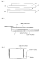
Fig. 1] Fig. 1 is a conceptual explanatory diagram of the metal foil with a carrier of the present invention comprising a structure in which a copper foil, a prepreg, a core material, and a copper foil are disposed in order, and the edge of the carrier A partially protrudes from the metal foil B. - [
Fig. 2] Fig. 2 is an explanatory diagram of the copper foil with a carrier of the present invention in which the glossy surface (S surface) of the carrier A and the glossy surface (S surface) of the metal foil B are mutually laminated. - [
Fig. 3] Fig. 3 is an explanatory diagram showing the bond part of the carrier A and the metal foil B of the present invention. - [
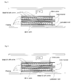
Fig. 4] Fig. 4 is an explanatory diagram showing a state of forming, based on hot pressing, a copper foil layer of L2 comprising a structure in which a copper foil, a prepreg, a core material, and a copper foil are disposed in order, and the edge of the carrier A partially protrudes from the metal foil B. - [
Fig. 5] Fig. 5 is an explanatory diagram showing a state of forming a copper foil layer as the outermost layer by hot pressing a copper foil with a carrier comprising a structure in which a copper foil, a prepreg, a core material, and a copper foil are placed in order, and the edge of the carrier A partially protrudes from the metal foil B, and in which the glossy surface of the carrier A and the glossy surface of the metal foil B are mutually bonded. - Generally, a printed circuit board is basically configured from a dielectric material referred to as a "prepreg" that is obtained by impregnating synthetic resin in a base material such as a synthetic resin plate, glass plate, nonwoven glass fabric or paper. A sheet such as a copper or copper alloy foil having electrical conductivity is bonded with the prepreg in-between. A laminate that is assembled as described above is generally referred to as a CCL, namely, Copper Clad Laminate material. In substitute for the foregoing copper or copper alloy foil used generally as the CCL material, other foils made of aluminum, nickel, zinc or the like are sometimes used. In the foregoing case, the foil thickness is roughly 5 to 200 µm.
- The metal foil with a carrier of the present invention is shown in
Fig. 1 . With the metal foil with a carrier shown inFig. 1 , the carrier is shown as A and the metal foil is shown as B. Although they look similar to the foregoing CCL material structurally, as for the metal foil with a carrier of the present invention, since the carrier A and the metal foil B are separated eventually, they can be easily peeled mechanically. On this point, since the CCL material cannot be peeled, the structure and function thereof are completely different from the present invention.
InFig. 1 , in both cases the carrier A is larger than the area of the metal foil B, and the case ofFig. 1 (a) shows a structure where two opposing sides protrude farther than the metal foil B, and the case ofFig. 1 (b) shows a structure where one side is protruding farther than the metal foil B.
The amount of protrusion can be suitably selected according to the workability, entirely as one thinks proper. This range is approximately 1 cm to 10 cm; however, it goes without saying that the protrusion may be prepared beyond the foregoing range. Although the remaining sides of the carrier A are desirably aligned with the metal foil B, this may be arbitrarily adjusted or selected according to the objective of the production process. - This is because the primary object of the present invention is to improve the handling performance of workers as a whole by realizing a structure where the carrier A protrudes from the metal foil B by enlarging the area of the carrier A to be greater than the metal foil B, facilitating the differentiation of a laminated pair of the carrier A and the metal foil B from a similar type of laminated pair of the carrier A and the metal foil B, and facilitating the peeling process by providing a part (edge or end) which differs in dimension upon peeling the carrier A from the metal foil B.
In normal circumstances, the carrier A and the metal foil B are formed in a quadrilateral, namely, a rectangular or a square. Although this shape is selectable so as long as it is convenient in the handling during its manufacture, a square or a rectangular is generally used. - In addition, from the perspective of handling in the layering process, desirably one side of the carrier A and one side of the metal foil B are mutually aligned, or two adjoining sides or two opposing sides of the carrier A and the metal foil B are mutually aligned. The foregoing selection is also optional.
With the carrier-attached metal foil of the present invention, a preferred mode is the metal foil B being a copper foil or a copper alloy foil, and the carrier A being a copper foil or a copper alloy foil.
The carrier-attached metal foil of the present invention yields numerous advantages as a result of the carrier A and the metal foil B respectively having a glossy surface, and the respective glossy surfaces being laminated to face each other, and this is also a preferred mode of lamination. -
Fig. 2 shows a metal foil with a carrier with a structure where the carrier A protrudes from the metal foil B by enlarging the carrier A to have a greater area than the metal foil B, and the respective glossy surfaces are laminated to face each other. InFig. 2 , the upper metal foil B has an upper surface using a copper foil as the M surface and a lower surface as the S surface, and the lower carrier A has an upper surface as the S surface and the lower surface as the M surface, and the S surfaces thereof are mutually bonded. - In the foregoing case, if the carrier A and the metal foil B are foils made of the same material, the respective front and back glossy surfaces of the carrier A and the metal foil B after peeling can be used without having to perform any reversing operations. This enables the considerable improvement in workability.
Conventionally, when a worker had to place the M surface of the copper foil on top and place the M surface on bottom in the layup (lamination) process and alternately repeat this process, there was a problem in that the work efficiency would deteriorate, but the present invention yields an effect of resolving the problem at once. - As described above, since the present invention has a structure where the carrier A protrudes from the metal foil B by enlarging the area of the carrier A to be greater than the metal foil B, it is possible to facilitate the differentiation of a laminated pair of the carrier A and the metal foil B from a similar type of laminated pair of the carrier A and the metal foil B, and facilitate the peeling process by providing a part (edge or end) which differs in dimension upon peeling the carrier A from the metal foil B. In summary, the present invention yields an effect of considerably improving the handling performance of workers compared to conventional processes, and the prominence of the present invention is evident.
- The carrier A and the metal foil B are mutually bonded to avoid misalignment, and these are desirably bonded by way of an adhesive, caulking, bi-fold or welding. The bonding method is also selectable, but the foregoing bonding methods are preferred.
Fig. 3 shows an example where the glossy surface of the carrier (for example, copper foil) A is placed on top and the glossy surface of the metal (copper) foil B is placed on bottom and welded based on ultrasonic welding. InFig. 3 , a part of the glossy surface of the carrier (for example, copper foil) A is exposed on the right side. And the rough surface of the metal (copper) foil B can be seen as the back side.
Since the carrier A and the metal foil B are fixed as described, the worker's layup (lamination) process is effectively improved. Moreover, since the surface is not fixed entirely, the peeling, or scaling process after lamination is also facilitated. - As the metal foil B, a copper foil or a copper alloy foil is a typical example and most favorable, but foils of aluminum, nickel, zinc and the like may also be used. Similarly, a foil of the same material as the metal foil B can be used as the carrier A.
In the case of a copper foil or a copper alloy foil, an electrolytic foil or a rolled foil with a thickness of 5 to 120 µm can be used. - Moreover, the coefficient of thermal expansion of the metal foil B is desirably within the range of +10% and -30% of the coefficient of thermal expansion of the metal foil B. Consequently, it is possible to effectively prevent the misalignment of the circuit caused by the difference in thermal expansion, and thereby minimize defective goods and improve the production yield.
Since the carrier A and the metal foil B are usually mechanically peeled before the process of plating or etching or the like, the peel strength thereof is desirably 1 g/cm or more and 1 kg/cm or less. Moreover, the peeling surface is desirably the boundary of the carrier A and the metal foil B. The residue of other material will require a removal work thereof and cause the overall process to become complicated, and must be avoided. - The Examples of the present invention are now explained. Note that these Examples are presented for facilitating the understanding of the invention, and the invention is not limited to the Examples. The present invention should be understood from the requirements described in the claims and the overall technical concept described in the specification, and the present invention covers all of the above.
- A prepreg prepared from epoxy resin was used as the resin material. An intended number of prepregs were laminated on the metal foil with a carrier, a two-layer printed circuit board referred to as an inner layer core was subsequently laminated thereon, a prepreg was subsequently laminated thereon, and a metal foil with a carrier was further formed thereon, in the foregoing order, in order to complete one set of a four-layer substrate material assembly unit.
Subsequently, this unit called "page" was repeatedly laminated about 10 times to configure a press assembly called "book". - The present invention is unique with respect to the structure of the metal foil with a carrier, and comprises a structure where the carrier A protrudes from the metal foil B.
Fig. 4 shows this structure.
Fig. 4 shows a case of forming a four-layer substrate unit called "page" obtained by laminating, in order, a metal foil with a carrier, intended number of prepregs, two-layer printed circuit board as an inner layer core, prepreg, and further a metal foil with a carrier.Fig. 4 shows a state of further stacking this with a mirror plate (intermediate plate) interposed therebetween (2 levels inFig. 4 ). In normal circumstances, this is repeated about 10 times to prepare an assembly called "book" to be pressed. Note that "x n" inFig. 4 shows a multilayer (n = 1, 2, 3...n). - These laminated bodies are mostly aligned, but the portion protruding to the right side of the foregoing unit is the characteristic point of this Example. This is the carrier A that protrudes from the metal foil B. A rolled copper alloy foil of 35 µm was used as the carrier A (in this example, brass containing 65% copper and 35% zinc was used), a rolled copper foil of 5 µm was used as the metal foil B, and these were bonded using an epoxy adhesive.
The bond location was the position shown inFig. 3 . Note that the bond surface of the carrier A and the metal foil B was the glossy surface of the carrier A and the rough surface of the metal foil B. - At the stage of preparing this set of four-layer substrate material assembly unit, it was necessary to reverse the metal foil with a carrier, but since the metal foil with a carrier comprises a structure where the carrier A protrudes from the metal foil B by enlarging the area of the carrier A to be greater than the metal foil B, it was possible to facilitate the differentiation of a laminated pair of the carrier A and the metal foil B from a similar type of laminated pair of the carrier A and the metal foil B, and the reversing operation was easy. Thus, it was possible to seek much improvement in the work efficiency at the previous step of preparing the assembly to be pressed.
- This book was thereafter set in a hot press and subject to compression molding at a prescribed temperature and pressure to produce a four-layer substrate. Note that substrates with four or more layers can be generally produced by a similar process by increasing the number of layers of the inner layer core.
- The laminated plate prepared as described above was formed into a completed product by peeling and separating the carrier from copper foil, and subsequently forming a circuit by undergoing plating process and/or etching process. Since the entire surface of the metal foil B is supported with the carrier A, the metal foil was completely free of wrinkles during the lamination.
In addition, since a copper alloy foil was used as the carrier A and copper was used as the metal foil B, the linear expansion coefficient was basically the same level as the copper foil as the constituent material of the substrate and the polymerized prepreg. Thus, the misalignment of the circuit did not occur. Accordingly, t was possible to minimize defective goods and thereby improve the production yield compared to cases of using a conventional CAC.
Example 1 is unique with respect to the structure of the carrier A that protrudes from the metal foil B, and it should be easy to understand that the advantage of this structure is not affected by the material or thickness of the metal foil B and the carrier A. - As with Example 1, a prepreg prepared from epoxy resin was used as the resin material. An intended number of prepregs were laminated on the metal foil with a carrier, a two-layer printed circuit board referred to as an inner layer core was subsequently laminated thereon, a prepreg was subsequently laminated thereon, and a metal foil with a carrier was further formed thereon, in the foregoing order, in order to complete one set of a four-layer substrate material assembly unit.
Subsequently, this unit called "page" was repeatedly laminated about 10 times to configure a press assembly called "book". - The present invention is unique with respect to the structure of the metal foil with a carrier, and comprises a structure where the carrier A protrudes from the metal foil B. Copper was used for both the carrier A and the metal foil B.
Fig. 5 shows this structure.Fig. 5 may appear to have the same structure asFig. 4 , but there are differences that are not shown, and, as described later, there is a difference in the materials that are used as the carrier A and the metal foil B, and the mode of these layered materials. The explanation ofFig. 5 is the same as Example 1.
Fig. 5 shows a case of forming a four-layer substrate unit called "page" obtained by laminating, in order, a metal foil with a carrier, intended number of prepregs, two-layer printed circuit board as an inner layer core, prepreg, and further a metal foil with a carrier.Fig. 5 shows a state of further stacking this with a mirror plate (intermediate plate) interposed therebetween (2 levels inFig. 5 ). In normal circumstances, this is repeated about 10 times to prepare an assembly called "book" to be pressed. Note that "x n" inFig. 5 shows a multilayer (n = 1, 2, 3...n). - These laminated bodies are mostly aligned, but the portion protruding to the right side of the foregoing unit. This is the carrier A that protrudes from the metal foil B. Moreover, a roller copper foil was used as the carrier A and an electrolytic copper foil was used as the metal foil B. Subsequently, the respective glossy surfaces were mutually bonded with the ultrasonic welding method. The bond location was the position shown in
Fig. 3 . As described above, it was possible to seek considerable improvement in the work efficiency at the previous step of preparing the assembly to be pressed. - And, the foregoing book was placed in the hot press and subject to compression molding at a prescribed temperature and pressure to produce a four-layer substrate. Generally, substrates with four or more layers can also be produced by a similar process by increasing the number of layers of the inner layer core.
- The printed circuit board of a multilayer structure with a prepreg prepared as described above was formed into a completed product by forming a circuit by undergoing plating process and/or etching process, and further peeling and separating the carrier A and the copper foil B. The metal foil was completely free of wrinkles during the foregoing lamination.
In addition, since a copper foil is used as the carrier A as well as the metal foil B, the linear expansion coefficient will basically be the same level as the copper foil as the constituent material of the substrate and the polymerized prepreg. Thus, the misalignment of the circuit will not occur. Accordingly, it was possible to minimize defective goods and thereby improve the production yield compared to cases of using a conventional CAC. - The roughened surface of the rolled copper foil of the carrier A and the S surface of the electrolytic copper foil of the metal foil B were bonded using the ultrasonic welding method. Otherwise, a book was prepared as with Example 2, and the foregoing book was placed in a hot press and subject to compression molding at a prescribed temperature and pressure to produce a four-layer substrate. The laminated plate prepared as described above was formed into a completed product by forming a circuit by undergoing plating process and/or etching process, and further peeling and separating the carrier and the copper foil.
With this peeling and separation, the configuration of this Example did not result in any rupture of the copper foil or residual copper carrier on the copper foil, though in the case of Example 2, the copper foil after the peeling and separation had slightly ruptured and the copper carrier slightly remained on the copper foil.
Accordingly, it was discovered that it is extremely effective to bond the roughened surface of the rolled copper foil of the carrier A and the S surface of the electrolytic copper foil of the metal foil B using the ultrasonic welding method. - An electrolytic copper foil was used as the carrier A. The electrolytic copper foil has a rough surface and a glossy surface, and here, the rough surface of the electrolytic copper foil and the S surface of the electrolytic copper foil of the metal foil B were bonded using the ultrasonic welding method. Otherwise, a book was prepared as with Example 3, and the foregoing book was placed in a hot press and subject to compression molding at a prescribed temperature and pressure to produce a four-layer substrate. The laminated plate prepared as described above was formed into a completed product by forming a circuit by undergoing plating process and/or etching process, and further peeling and separating the carrier and the copper foil.
The configuration of this Example did not result in any rupture of the copper foil or residual copper carrier on the copper foil, as with Example 3.
Accordingly, it was discovered that it is extremely effective to bond the rough surface of the electrolytic copper foil of the carrier A and the S surface of the electrolytic copper foil of the metal foil B using the ultrasonic welding method. - An aluminum rolled foil was used as the carrier A, and it was bonded with the S surface of the electrolytic copper foil of the metal foil B using the ultrasonic welding method. Otherwise, a book was prepared as with Example 2, and the foregoing book was placed in a hot press and subject to compression molding at a prescribed temperature and pressure to produce a four-layer substrate. The laminated plate prepared as described above was formed into a completed product by forming a circuit by undergoing plating process and/or etching process, and further peeling and separating the carrier and the copper foil.
The configuration of this Example did not result in any rupture of the copper foil or residual copper carrier on the copper foil in the peeling and separation process, as with Example 3. - A copper foil or a copper alloy foil is normally used as the metal foil B, but it goes without saying that other metal foils may be used as the metal foil B. Moreover, as the carrier A, a copper foil or a copper alloy foil or an aluminum foil is used. In the foregoing case, rolled aluminum foil is generally used.
As the copper foil, there is a rolled copper foil and an electrolytic copper foil, but either may be used as the carrier A of the present invention. The glossy surface of the rolled copper foil and the electrolytic copper foil may be used, or the rough surface thereof may be used. - In the case of a rolled copper foil, since the rolled surface is the glossy surface, this may be used upon performing roughening treatment thereto. In the case of an electrolytic copper foil, the glossy surface or the rough surface may be further subject to roughening treatment and used as the carrier A.
Based on the selection of the material of the carrier A and the metal foil B; particularly, by selecting the material and the surface state, the peelability upon separating the bond can improve. Thus, these can be arbitrarily combined and used. - The metal foil with a carrier of the present invention is characterized in that it is a laminated body in which a carrier A and a metal foil B are placed alternately, wherein the metal foil with a carrier comprises a structure where the adjoining carrier A has an area which covers the entire surface of the metal foil B, and the edge of the carrier A protrudes partially or entirely from the metal foil B. Thus, it is therefore easy to differentiate a laminated pair of the carrier A and the metal foil B from a similar type of laminated pair of the carrier A and the metal foil B, and the worker's handling performance will improve. Moreover, even upon peeling the carrier from the copper foil, peeling is easy since there is a part (edge or end) which differs in dimension.
- Although it is optional to mutually face the glossy surface of the carrier A and the glossy surface of the metal foil B, when it is placed this way, the work efficiency will improve dramatically since the worker no longer needs to perform operations of placing the M surface of the copper foil on bottom or top.
In addition, although the use of a copper foil as the carrier is optional, if the carrier is made of copper foil, the linear expansion coefficient will be of the same level as the copper foil as the constituent material of the substrate and the polymerized prepreg, and, since the misalignment of the circuit will not occur, the present invention yields a superior effect of minimizing defective goods and thereby improving the production yield.
Significant advantages are yielded by the metal foil with a carrier obtained with the present invention, and this metal foil with a carrier is particularly effective for producing a printed circuit board.
Claims (10)
- A metal foil with a carrier as a laminated body in which a carrier A and a metal foil B are placed alternately, wherein the metal foil with a carrier comprises a structure where the adjoining carrier A has an area which covers the entire surface of the metal foil B, and the edge of the carrier A protrudes partially or entirely from the metal foil B.
- The metal foil with a carrier according to claim 1, wherein the carrier A and the metal foil B are rectangular.
- The metal foil with a carrier according to claim 2, wherein one side of the carrier A and one side of the metal foil B are mutually aligned.
- The metal foil with a carrier according to claim 2, wherein two adjoining sides or two opposing sides of the carrier A and the metal foil B are mutually aligned.
- The metal foil with a carrier according to any one of claims 1 to 4, wherein the metal foil B is a copper foil or a copper alloy foil.
- A copper foil with a carrier, wherein a glossy surface of a metal foil B is subject to ultrasonic bonding so as to come in contact with a carrier A made of aluminum or copper or copper alloy.
- The metal foil with a carrier according to any one of claims 1 to 5, wherein a glossy surface of the metal foil B is subject to ultrasonic bonding so as to come in contact with the carrier A made of aluminum or copper or copper alloy.
- The copper foil with a carrier according to claim 6 or claim 7, wherein the carrier A is a rolled copper foil or an electrolytic copper foil, and the glossy surface of the copper foil B is subject to ultrasonic bonding so as to come in contact with a roughened surface of the rolled copper foil or a rough surface or a roughened surface of the electrolytic copper foil.
- The metal foil with a carrier according to any one of claims 1 to 8, wherein the carrier A and the metal foil B respectively have a glossy surface, and are laminated so that the respective glossy surfaces mutually face each other.
- The metal foil with a carrier according to any one claims 1 to 9, wherein the carrier A and the metal foil B are bonded by way of an adhesive, caulking, bi-fold or welding so that they do not become misaligned.
Applications Claiming Priority (2)
| Application Number | Priority Date | Filing Date | Title |
|---|---|---|---|
| JP2008327448A JP2009143233A (en) | 2008-12-24 | 2008-12-24 | Metal foil with carrier |
| PCT/JP2009/054481 WO2010073744A1 (en) | 2008-12-24 | 2009-03-10 | Metal foil with carrier |
Publications (3)
| Publication Number | Publication Date |
|---|---|
| EP2383113A1 true EP2383113A1 (en) | 2011-11-02 |
| EP2383113A4 EP2383113A4 (en) | 2013-01-16 |
| EP2383113B1 EP2383113B1 (en) | 2016-05-04 |
Family
ID=40914417
Family Applications (1)
| Application Number | Title | Priority Date | Filing Date |
|---|---|---|---|
| EP09834550.7A Not-in-force EP2383113B1 (en) | 2008-12-24 | 2009-03-10 | Metal foil with carrier |
Country Status (7)
| Country | Link |
|---|---|
| US (1) | US20110250468A1 (en) |
| EP (1) | EP2383113B1 (en) |
| JP (2) | JP2009143233A (en) |
| KR (3) | KR20110081339A (en) |
| CN (2) | CN105208771A (en) |
| SG (1) | SG171718A1 (en) |
| WO (1) | WO2010073744A1 (en) |
Families Citing this family (13)
| Publication number | Priority date | Publication date | Assignee | Title |
|---|---|---|---|---|
| EP2589488A1 (en) * | 2009-12-22 | 2013-05-08 | JX Nippon Mining & Metals Corporation | Rectangular laminated body |
| JP5697892B2 (en) * | 2010-05-11 | 2015-04-08 | Jx日鉱日石金属株式会社 | Copper foil laminate and method for producing laminate |
| JP5165773B2 (en) | 2011-02-10 | 2013-03-21 | フリージア・マクロス株式会社 | Metal foil with carrier and method for producing laminated substrate using the same |
| JP2013069745A (en) * | 2011-09-21 | 2013-04-18 | Panasonic Corp | Support body and method for manufacturing printed wiring board |
| JP5190553B1 (en) * | 2012-03-06 | 2013-04-24 | フリージア・マクロス株式会社 | Metal foil with carrier |
| JP6063183B2 (en) * | 2012-08-31 | 2017-01-18 | パナソニックIpマネジメント株式会社 | Peelable copper foil substrate and circuit board manufacturing method |
| TWI551436B (en) * | 2012-09-24 | 2016-10-01 | Jx日鑛日石金屬股份有限公司 | A carrier metal foil, a laminate made of a resin-made plate-like carrier and a metal foil, and the like |
| US20150353967A1 (en) | 2013-01-11 | 2015-12-10 | Veolia Water Solutions & Technologies Support | Method for increased productivity of polyhydroxyalkanoates (phas) in fed-batch processes for biomass derived from the treatment of wastewater |
| WO2016143117A1 (en) * | 2015-03-12 | 2016-09-15 | 三井金属鉱業株式会社 | Metal foil with carrier, and manufacturing method for wiring board |
| CN105856729B (en) * | 2016-04-25 | 2018-01-19 | 江苏博敏电子有限公司 | A kind of aliasing copper foil and its aliasing method |
| JP7085419B2 (en) * | 2018-03-14 | 2022-06-16 | 東洋鋼鈑株式会社 | Rolled joint and its manufacturing method |
| CN110126372A (en) * | 2019-06-05 | 2019-08-16 | 河源广工大协同创新研究院 | A kind of preparation method of multiple layer metal layers of foil structure copper-clad plate |
| CN118124242B (en) * | 2024-02-22 | 2025-11-18 | 中国航空制造技术研究院 | A method for surface treatment of metal foil before bonding of laminates |
Family Cites Families (40)
| Publication number | Priority date | Publication date | Assignee | Title |
|---|---|---|---|---|
| US1583381A (en) * | 1918-12-13 | 1926-05-04 | James G Zimmerman | Film pack |
| JPS5222380B2 (en) * | 1973-05-30 | 1977-06-17 | ||
| US3998601A (en) * | 1973-12-03 | 1976-12-21 | Yates Industries, Inc. | Thin foil |
| US4861648A (en) * | 1988-03-14 | 1989-08-29 | Gila River Products, Inc. | Materials for laminating flexible printed circuits |
| US5066366A (en) * | 1990-05-04 | 1991-11-19 | Olin Corporation | Method for making foil |
| US5153050A (en) | 1991-08-27 | 1992-10-06 | Johnston James A | Component of printed circuit boards |
| US5829124A (en) * | 1995-12-29 | 1998-11-03 | International Business Machines Corporation | Method for forming metallized patterns on the top surface of a printed circuit board |
| US5942314A (en) * | 1997-04-17 | 1999-08-24 | Mitsui Mining & Smelting Co., Ltd. | Ultrasonic welding of copper foil |
| US6596391B2 (en) * | 1997-05-14 | 2003-07-22 | Honeywell International Inc. | Very ultra thin conductor layers for printed wiring boards |
| JPH11277562A (en) * | 1998-03-31 | 1999-10-12 | Hitachi Chem Co Ltd | Carrier plate for manufacturing copper-clad laminate |
| US6355360B1 (en) * | 1998-04-10 | 2002-03-12 | R.E. Service Company, Inc. | Separator sheet laminate for use in the manufacture of printed circuit boards |
| US6129990A (en) * | 1998-04-10 | 2000-10-10 | R. E. Service Company, Inc. | Copper/steel laminated sheet for use in manufacturing printed circuit boards |
| IT1305116B1 (en) * | 1998-09-14 | 2001-04-10 | Zincocelere Spa | COMPONENT FOR MULTILAYER PRINTED CIRCUIT, METHOD FOR SUABABRICATION AND RELATED MULTI-PURPOSE PRINTED CIRCUIT. |
| DE19859613C2 (en) * | 1998-12-23 | 2001-09-06 | Buerkle Gmbh Robert | Press pack construction and process for its production |
| JP3370624B2 (en) * | 1999-08-24 | 2003-01-27 | 三井金属鉱業株式会社 | Electrolytic copper foil with carrier foil and copper-clad laminate using the electrolytic copper foil |
| JP2001068804A (en) * | 1999-08-31 | 2001-03-16 | Mitsui Mining & Smelting Co Ltd | Electrolytic copper foil with carrier foil, method for producing the electrolytic copper foil, and copper-clad laminate using the electrolytic copper foil |
| JP3676152B2 (en) | 1999-11-11 | 2005-07-27 | 三井金属鉱業株式会社 | Electrolytic copper foil with carrier foil and method for producing the same |
| JP3670179B2 (en) * | 1999-11-11 | 2005-07-13 | 三井金属鉱業株式会社 | Electrolytic copper foil with carrier foil and copper-clad laminate using the electrolytic copper foil with carrier foil |
| TWI299699B (en) * | 2000-02-14 | 2008-08-11 | Kaneka Corp | Laminate comprising polyimide and conductor layer, wiring board with the use of the same and process for producing the same |
| US6346335B1 (en) * | 2000-03-10 | 2002-02-12 | Olin Corporation | Copper foil composite including a release layer |
| US6606792B1 (en) * | 2000-05-25 | 2003-08-19 | Oak-Mitsui, Inc. | Process to manufacturing tight tolerance embedded elements for printed circuit boards |
| US7026059B2 (en) * | 2000-09-22 | 2006-04-11 | Circuit Foil Japan Co., Ltd. | Copper foil for high-density ultrafine printed wiring boad |
| JP2002134877A (en) * | 2000-10-10 | 2002-05-10 | Morton Internatl Inc | Mounting and processing of thin film materials |
| CN1279796C (en) * | 2000-10-17 | 2006-10-11 | 莫顿国际公司 | Method for fixing and handling thin film materials |
| TW532050B (en) * | 2000-11-09 | 2003-05-11 | Matsushita Electric Industrial Co Ltd | Circuit board and method for manufacturing the same |
| JP2003051673A (en) * | 2001-08-06 | 2003-02-21 | Mitsui Mining & Smelting Co Ltd | Copper foil for printed wiring board and copper-clad laminate using the copper foil for printed wiring board |
| JP4379854B2 (en) * | 2001-10-30 | 2009-12-09 | 日鉱金属株式会社 | Surface treated copper foil |
| US6984456B2 (en) * | 2002-05-13 | 2006-01-10 | Mitsui Mining & Smelting Co., Ltd. | Flexible printed wiring board for chip-on flexibles |
| JP4216044B2 (en) * | 2002-10-31 | 2009-01-28 | 三井金属鉱業株式会社 | Ultrasonic welding equipment for metal foil |
| US6994918B2 (en) * | 2003-08-12 | 2006-02-07 | Johnson Morgan T | Selective application of conductive material to circuit boards by pick and place |
| JP4087369B2 (en) | 2003-11-11 | 2008-05-21 | 古河サーキットフォイル株式会社 | Ultra-thin copper foil with carrier and printed wiring board |
| JP4699261B2 (en) * | 2005-03-31 | 2011-06-08 | 新日鐵化学株式会社 | Multilayer laminate and flexible copper-clad laminate |
| GB0515584D0 (en) * | 2005-07-28 | 2005-09-07 | Glaxo Group Ltd | Medicament dispenser |
| JP4927503B2 (en) * | 2005-12-15 | 2012-05-09 | 古河電気工業株式会社 | Ultra-thin copper foil with carrier and printed wiring board |
| CN1984527B (en) * | 2005-12-15 | 2010-12-01 | 古河电气工业株式会社 | Ultrathin copper foil with carrier and printed circuit board |
| JP2007214427A (en) * | 2006-02-10 | 2007-08-23 | Shinko Electric Ind Co Ltd | Wiring board manufacturing method |
| CN101573477B (en) * | 2006-12-28 | 2011-01-19 | 日矿金属株式会社 | Roll unit for use in surface treatment of copper foil |
| CN101578397B (en) * | 2006-12-28 | 2011-02-02 | Jx日矿日石金属株式会社 | Roll unit dipped in surface treatment liquid |
| JP2007186797A (en) | 2007-02-15 | 2007-07-26 | Furukawa Circuit Foil Kk | Method for producing ultrathin copper foil with carrier, ultrathin copper foil produced by the production method, and printed circuit board, multilayer printed circuit board and wiring board for chip on film using the ultrathin copper foil |
| WO2009154066A1 (en) * | 2008-06-17 | 2009-12-23 | 日鉱金属株式会社 | Copper foil for printed circuit board and copper clad laminate plate for printed circuit board |
-
2008
- 2008-12-24 JP JP2008327448A patent/JP2009143233A/en active Pending
-
2009
- 2009-03-10 KR KR1020117012610A patent/KR20110081339A/en not_active Ceased
- 2009-03-10 SG SG2011032448A patent/SG171718A1/en unknown
- 2009-03-10 EP EP09834550.7A patent/EP2383113B1/en not_active Not-in-force
- 2009-03-10 WO PCT/JP2009/054481 patent/WO2010073744A1/en not_active Ceased
- 2009-03-10 CN CN201510484111.9A patent/CN105208771A/en active Pending
- 2009-03-10 CN CN200980152431.7A patent/CN102264540B/en not_active Expired - Fee Related
- 2009-03-10 KR KR1020137030727A patent/KR20130136005A/en not_active Ceased
- 2009-03-10 JP JP2010543933A patent/JP5485915B2/en not_active Expired - Fee Related
- 2009-03-10 US US13/132,697 patent/US20110250468A1/en not_active Abandoned
- 2009-03-10 KR KR1020157020564A patent/KR20150093247A/en not_active Ceased
Also Published As
| Publication number | Publication date |
|---|---|
| WO2010073744A1 (en) | 2010-07-01 |
| CN105208771A (en) | 2015-12-30 |
| CN102264540A (en) | 2011-11-30 |
| JP2009143233A (en) | 2009-07-02 |
| JP5485915B2 (en) | 2014-05-07 |
| US20110250468A1 (en) | 2011-10-13 |
| CN102264540B (en) | 2017-02-08 |
| KR20130136005A (en) | 2013-12-11 |
| KR20150093247A (en) | 2015-08-17 |
| SG171718A1 (en) | 2011-07-28 |
| JPWO2010073744A1 (en) | 2012-06-14 |
| EP2383113A4 (en) | 2013-01-16 |
| EP2383113B1 (en) | 2016-05-04 |
| KR20110081339A (en) | 2011-07-13 |
Similar Documents
| Publication | Publication Date | Title |
|---|---|---|
| EP2383113B1 (en) | Metal foil with carrier | |
| JP4805304B2 (en) | Metal foil with carrier and method for producing multilayer coreless circuit board | |
| EP2383114B1 (en) | Metal foil with carrier | |
| EP2361762B1 (en) | Method for producing laminate | |
| JP5647310B2 (en) | Manufacturing method of multilayer coreless circuit board, manufacturing method of multilayer body for multilayer printed wiring board, manufacturing method of multilayer body used for manufacturing multilayer printed wiring board, and manufacturing method of printed circuit board | |
| JP2017183459A (en) | Copper foil, copper clad laminate sheet, flexible printed circuit board and electronic apparatus | |
| JP5697892B2 (en) | Copper foil laminate and method for producing laminate | |
| JP5847882B2 (en) | Method for manufacturing laminate for multilayer printed wiring board and method for manufacturing printed circuit board | |
| JP5427847B2 (en) | Metal foil with carrier | |
| CN110650597B (en) | Circuit board, manufacturing method thereof and electronic equipment | |
| JP3234543B2 (en) | Plate for forming metal foil-clad laminate, method for producing metal-foil-clad laminate, method for producing metal-foil-clad laminate | |
| JP2004079594A (en) | Multi-layer flexible printed wiring board | |
| JPH0259337A (en) | Manufacturing method for copper foil-clad circuit board | |
| JP2003188545A (en) | Laminated sheet | |
| JP2010177294A (en) | Method of manufacturing multilayer plate |
Legal Events
| Date | Code | Title | Description |
|---|---|---|---|
| PUAI | Public reference made under article 153(3) epc to a published international application that has entered the european phase |
Free format text: ORIGINAL CODE: 0009012 |
|
| 17P | Request for examination filed |
Effective date: 20110505 |
|
| AK | Designated contracting states |
Kind code of ref document: A1 Designated state(s): AT BE BG CH CY CZ DE DK EE ES FI FR GB GR HR HU IE IS IT LI LT LU LV MC MK MT NL NO PL PT RO SE SI SK TR |
|
| DAX | Request for extension of the european patent (deleted) | ||
| A4 | Supplementary search report drawn up and despatched |
Effective date: 20121217 |
|
| RIC1 | Information provided on ipc code assigned before grant |
Ipc: H05K 3/02 20060101AFI20121211BHEP Ipc: H05K 3/46 20060101ALN20121211BHEP |
|
| 17Q | First examination report despatched |
Effective date: 20140620 |
|
| REG | Reference to a national code |
Ref country code: DE Ref legal event code: R079 Ref document number: 602009038512 Country of ref document: DE Free format text: PREVIOUS MAIN CLASS: B32B0015200000 Ipc: H05K0003020000 |
|
| GRAP | Despatch of communication of intention to grant a patent |
Free format text: ORIGINAL CODE: EPIDOSNIGR1 |
|
| RIC1 | Information provided on ipc code assigned before grant |
Ipc: H05K 3/02 20060101AFI20151214BHEP Ipc: H05K 3/46 20060101ALN20151214BHEP |
|
| INTG | Intention to grant announced |
Effective date: 20160111 |
|
| GRAS | Grant fee paid |
Free format text: ORIGINAL CODE: EPIDOSNIGR3 |
|
| GRAA | (expected) grant |
Free format text: ORIGINAL CODE: 0009210 |
|
| AK | Designated contracting states |
Kind code of ref document: B1 Designated state(s): AT BE BG CH CY CZ DE DK EE ES FI FR GB GR HR HU IE IS IT LI LT LU LV MC MK MT NL NO PL PT RO SE SI SK TR |
|
| REG | Reference to a national code |
Ref country code: GB Ref legal event code: FG4D |
|
| REG | Reference to a national code |
Ref country code: CH Ref legal event code: EP |
|
| REG | Reference to a national code |
Ref country code: AT Ref legal event code: REF Ref document number: 797868 Country of ref document: AT Kind code of ref document: T Effective date: 20160515 |
|
| REG | Reference to a national code |
Ref country code: IE Ref legal event code: FG4D |
|
| REG | Reference to a national code |
Ref country code: DE Ref legal event code: R096 Ref document number: 602009038512 Country of ref document: DE |
|
| REG | Reference to a national code |
Ref country code: NL Ref legal event code: MP Effective date: 20160504 |
|
| REG | Reference to a national code |
Ref country code: LT Ref legal event code: MG4D |
|
| PG25 | Lapsed in a contracting state [announced via postgrant information from national office to epo] |
Ref country code: FI Free format text: LAPSE BECAUSE OF FAILURE TO SUBMIT A TRANSLATION OF THE DESCRIPTION OR TO PAY THE FEE WITHIN THE PRESCRIBED TIME-LIMIT Effective date: 20160504 Ref country code: NL Free format text: LAPSE BECAUSE OF FAILURE TO SUBMIT A TRANSLATION OF THE DESCRIPTION OR TO PAY THE FEE WITHIN THE PRESCRIBED TIME-LIMIT Effective date: 20160504 Ref country code: LT Free format text: LAPSE BECAUSE OF FAILURE TO SUBMIT A TRANSLATION OF THE DESCRIPTION OR TO PAY THE FEE WITHIN THE PRESCRIBED TIME-LIMIT Effective date: 20160504 Ref country code: NO Free format text: LAPSE BECAUSE OF FAILURE TO SUBMIT A TRANSLATION OF THE DESCRIPTION OR TO PAY THE FEE WITHIN THE PRESCRIBED TIME-LIMIT Effective date: 20160804 |
|
| REG | Reference to a national code |
Ref country code: AT Ref legal event code: MK05 Ref document number: 797868 Country of ref document: AT Kind code of ref document: T Effective date: 20160504 |
|
| PG25 | Lapsed in a contracting state [announced via postgrant information from national office to epo] |
Ref country code: GR Free format text: LAPSE BECAUSE OF FAILURE TO SUBMIT A TRANSLATION OF THE DESCRIPTION OR TO PAY THE FEE WITHIN THE PRESCRIBED TIME-LIMIT Effective date: 20160805 Ref country code: HR Free format text: LAPSE BECAUSE OF FAILURE TO SUBMIT A TRANSLATION OF THE DESCRIPTION OR TO PAY THE FEE WITHIN THE PRESCRIBED TIME-LIMIT Effective date: 20160504 Ref country code: SE Free format text: LAPSE BECAUSE OF FAILURE TO SUBMIT A TRANSLATION OF THE DESCRIPTION OR TO PAY THE FEE WITHIN THE PRESCRIBED TIME-LIMIT Effective date: 20160504 Ref country code: LV Free format text: LAPSE BECAUSE OF FAILURE TO SUBMIT A TRANSLATION OF THE DESCRIPTION OR TO PAY THE FEE WITHIN THE PRESCRIBED TIME-LIMIT Effective date: 20160504 Ref country code: PT Free format text: LAPSE BECAUSE OF FAILURE TO SUBMIT A TRANSLATION OF THE DESCRIPTION OR TO PAY THE FEE WITHIN THE PRESCRIBED TIME-LIMIT Effective date: 20160905 Ref country code: ES Free format text: LAPSE BECAUSE OF FAILURE TO SUBMIT A TRANSLATION OF THE DESCRIPTION OR TO PAY THE FEE WITHIN THE PRESCRIBED TIME-LIMIT Effective date: 20160504 |
|
| PG25 | Lapsed in a contracting state [announced via postgrant information from national office to epo] |
Ref country code: IT Free format text: LAPSE BECAUSE OF FAILURE TO SUBMIT A TRANSLATION OF THE DESCRIPTION OR TO PAY THE FEE WITHIN THE PRESCRIBED TIME-LIMIT Effective date: 20160504 |
|
| PG25 | Lapsed in a contracting state [announced via postgrant information from national office to epo] |
Ref country code: CZ Free format text: LAPSE BECAUSE OF FAILURE TO SUBMIT A TRANSLATION OF THE DESCRIPTION OR TO PAY THE FEE WITHIN THE PRESCRIBED TIME-LIMIT Effective date: 20160504 Ref country code: SK Free format text: LAPSE BECAUSE OF FAILURE TO SUBMIT A TRANSLATION OF THE DESCRIPTION OR TO PAY THE FEE WITHIN THE PRESCRIBED TIME-LIMIT Effective date: 20160504 Ref country code: RO Free format text: LAPSE BECAUSE OF FAILURE TO SUBMIT A TRANSLATION OF THE DESCRIPTION OR TO PAY THE FEE WITHIN THE PRESCRIBED TIME-LIMIT Effective date: 20160504 Ref country code: EE Free format text: LAPSE BECAUSE OF FAILURE TO SUBMIT A TRANSLATION OF THE DESCRIPTION OR TO PAY THE FEE WITHIN THE PRESCRIBED TIME-LIMIT Effective date: 20160504 Ref country code: DK Free format text: LAPSE BECAUSE OF FAILURE TO SUBMIT A TRANSLATION OF THE DESCRIPTION OR TO PAY THE FEE WITHIN THE PRESCRIBED TIME-LIMIT Effective date: 20160504 |
|
| REG | Reference to a national code |
Ref country code: DE Ref legal event code: R097 Ref document number: 602009038512 Country of ref document: DE |
|
| PG25 | Lapsed in a contracting state [announced via postgrant information from national office to epo] |
Ref country code: BE Free format text: LAPSE BECAUSE OF FAILURE TO SUBMIT A TRANSLATION OF THE DESCRIPTION OR TO PAY THE FEE WITHIN THE PRESCRIBED TIME-LIMIT Effective date: 20160504 Ref country code: PL Free format text: LAPSE BECAUSE OF FAILURE TO SUBMIT A TRANSLATION OF THE DESCRIPTION OR TO PAY THE FEE WITHIN THE PRESCRIBED TIME-LIMIT Effective date: 20160504 Ref country code: AT Free format text: LAPSE BECAUSE OF FAILURE TO SUBMIT A TRANSLATION OF THE DESCRIPTION OR TO PAY THE FEE WITHIN THE PRESCRIBED TIME-LIMIT Effective date: 20160504 |
|
| PLBE | No opposition filed within time limit |
Free format text: ORIGINAL CODE: 0009261 |
|
| STAA | Information on the status of an ep patent application or granted ep patent |
Free format text: STATUS: NO OPPOSITION FILED WITHIN TIME LIMIT |
|
| 26N | No opposition filed |
Effective date: 20170207 |
|
| PG25 | Lapsed in a contracting state [announced via postgrant information from national office to epo] |
Ref country code: SI Free format text: LAPSE BECAUSE OF FAILURE TO SUBMIT A TRANSLATION OF THE DESCRIPTION OR TO PAY THE FEE WITHIN THE PRESCRIBED TIME-LIMIT Effective date: 20160504 |
|
| REG | Reference to a national code |
Ref country code: LU Ref legal event code: TE Owner name: JX NIPPON MINING METALS CORPORATION; JP Effective date: 20170524 Ref country code: LU Ref legal event code: TE Owner name: JX NIPPON MINING & METALS CORPORATION; JP Effective date: 20170524 |
|
| REG | Reference to a national code |
Ref country code: CH Ref legal event code: PL |
|
| GBPC | Gb: european patent ceased through non-payment of renewal fee |
Effective date: 20170310 |
|
| PG25 | Lapsed in a contracting state [announced via postgrant information from national office to epo] |
Ref country code: MC Free format text: LAPSE BECAUSE OF FAILURE TO SUBMIT A TRANSLATION OF THE DESCRIPTION OR TO PAY THE FEE WITHIN THE PRESCRIBED TIME-LIMIT Effective date: 20160504 |
|
| REG | Reference to a national code |
Ref country code: IE Ref legal event code: MM4A |
|
| REG | Reference to a national code |
Ref country code: FR Ref legal event code: ST Effective date: 20171130 |
|
| PG25 | Lapsed in a contracting state [announced via postgrant information from national office to epo] |
Ref country code: FR Free format text: LAPSE BECAUSE OF NON-PAYMENT OF DUE FEES Effective date: 20170331 |
|
| PG25 | Lapsed in a contracting state [announced via postgrant information from national office to epo] |
Ref country code: GB Free format text: LAPSE BECAUSE OF NON-PAYMENT OF DUE FEES Effective date: 20170310 Ref country code: CH Free format text: LAPSE BECAUSE OF NON-PAYMENT OF DUE FEES Effective date: 20170331 Ref country code: LI Free format text: LAPSE BECAUSE OF NON-PAYMENT OF DUE FEES Effective date: 20170331 Ref country code: IE Free format text: LAPSE BECAUSE OF NON-PAYMENT OF DUE FEES Effective date: 20170310 |
|
| PG25 | Lapsed in a contracting state [announced via postgrant information from national office to epo] |
Ref country code: MT Free format text: LAPSE BECAUSE OF NON-PAYMENT OF DUE FEES Effective date: 20170310 |
|
| PG25 | Lapsed in a contracting state [announced via postgrant information from national office to epo] |
Ref country code: HU Free format text: LAPSE BECAUSE OF FAILURE TO SUBMIT A TRANSLATION OF THE DESCRIPTION OR TO PAY THE FEE WITHIN THE PRESCRIBED TIME-LIMIT; INVALID AB INITIO Effective date: 20090310 |
|
| PG25 | Lapsed in a contracting state [announced via postgrant information from national office to epo] |
Ref country code: BG Free format text: LAPSE BECAUSE OF FAILURE TO SUBMIT A TRANSLATION OF THE DESCRIPTION OR TO PAY THE FEE WITHIN THE PRESCRIBED TIME-LIMIT Effective date: 20160504 |
|
| PG25 | Lapsed in a contracting state [announced via postgrant information from national office to epo] |
Ref country code: CY Free format text: LAPSE BECAUSE OF NON-PAYMENT OF DUE FEES Effective date: 20160504 |
|
| PG25 | Lapsed in a contracting state [announced via postgrant information from national office to epo] |
Ref country code: MK Free format text: LAPSE BECAUSE OF FAILURE TO SUBMIT A TRANSLATION OF THE DESCRIPTION OR TO PAY THE FEE WITHIN THE PRESCRIBED TIME-LIMIT Effective date: 20160504 |
|
| PG25 | Lapsed in a contracting state [announced via postgrant information from national office to epo] |
Ref country code: TR Free format text: LAPSE BECAUSE OF FAILURE TO SUBMIT A TRANSLATION OF THE DESCRIPTION OR TO PAY THE FEE WITHIN THE PRESCRIBED TIME-LIMIT Effective date: 20160504 |
|
| PG25 | Lapsed in a contracting state [announced via postgrant information from national office to epo] |
Ref country code: IS Free format text: LAPSE BECAUSE OF FAILURE TO SUBMIT A TRANSLATION OF THE DESCRIPTION OR TO PAY THE FEE WITHIN THE PRESCRIBED TIME-LIMIT Effective date: 20160904 |
|
| REG | Reference to a national code |
Ref country code: LU Ref legal event code: HC Owner name: JX NIPPON MINING & METALS CORPORATION; JP Free format text: FORMER OWNER: JX NIPPON MINING & METALS CORPORATION Effective date: 20210315 |
|
| PGFP | Annual fee paid to national office [announced via postgrant information from national office to epo] |
Ref country code: LU Payment date: 20240227 Year of fee payment: 16 |
|
| PGFP | Annual fee paid to national office [announced via postgrant information from national office to epo] |
Ref country code: DE Payment date: 20240130 Year of fee payment: 16 |
|
| REG | Reference to a national code |
Ref country code: DE Ref legal event code: R119 Ref document number: 602009038512 Country of ref document: DE |
|
| PG25 | Lapsed in a contracting state [announced via postgrant information from national office to epo] |
Ref country code: LU Free format text: LAPSE BECAUSE OF NON-PAYMENT OF DUE FEES Effective date: 20250310 |
|
| PG25 | Lapsed in a contracting state [announced via postgrant information from national office to epo] |
Ref country code: DE Free format text: LAPSE BECAUSE OF NON-PAYMENT OF DUE FEES Effective date: 20251001 |