EP2381756A2 - Electromagnetic wave absorber - Google Patents
Electromagnetic wave absorber Download PDFInfo
- Publication number
- EP2381756A2 EP2381756A2 EP11003179A EP11003179A EP2381756A2 EP 2381756 A2 EP2381756 A2 EP 2381756A2 EP 11003179 A EP11003179 A EP 11003179A EP 11003179 A EP11003179 A EP 11003179A EP 2381756 A2 EP2381756 A2 EP 2381756A2
- Authority
- EP
- European Patent Office
- Prior art keywords
- electromagnetic wave
- wave absorber
- dielectric layer
- conductive films
- relative permittivity
- Prior art date
- Legal status (The legal status is an assumption and is not a legal conclusion. Google has not performed a legal analysis and makes no representation as to the accuracy of the status listed.)
- Withdrawn
Links
- 239000006096 absorbing agent Substances 0.000 title claims abstract description 140
- 239000000463 material Substances 0.000 claims description 23
- OKTJSMMVPCPJKN-UHFFFAOYSA-N Carbon Chemical compound [C] OKTJSMMVPCPJKN-UHFFFAOYSA-N 0.000 claims description 12
- 229910002804 graphite Inorganic materials 0.000 claims description 12
- 239000010439 graphite Substances 0.000 claims description 12
- 229920005992 thermoplastic resin Polymers 0.000 claims description 6
- 239000012815 thermoplastic material Substances 0.000 claims description 4
- 239000010410 layer Substances 0.000 description 108
- 238000010521 absorption reaction Methods 0.000 description 53
- 238000005259 measurement Methods 0.000 description 19
- 239000012790 adhesive layer Substances 0.000 description 10
- 239000004820 Pressure-sensitive adhesive Substances 0.000 description 9
- 229920002313 fluoropolymer Polymers 0.000 description 8
- RYGMFSIKBFXOCR-UHFFFAOYSA-N Copper Chemical compound [Cu] RYGMFSIKBFXOCR-UHFFFAOYSA-N 0.000 description 6
- 239000000853 adhesive Substances 0.000 description 5
- 229910052782 aluminium Inorganic materials 0.000 description 5
- XAGFODPZIPBFFR-UHFFFAOYSA-N aluminium Chemical compound [Al] XAGFODPZIPBFFR-UHFFFAOYSA-N 0.000 description 5
- 239000006185 dispersion Substances 0.000 description 5
- 238000011156 evaluation Methods 0.000 description 5
- 238000000034 method Methods 0.000 description 5
- -1 polyethylene Polymers 0.000 description 5
- 229920005989 resin Polymers 0.000 description 5
- 239000011347 resin Substances 0.000 description 5
- 239000011889 copper foil Substances 0.000 description 4
- 230000001747 exhibiting effect Effects 0.000 description 4
- 239000007769 metal material Substances 0.000 description 4
- 229920003229 poly(methyl methacrylate) Polymers 0.000 description 4
- 239000004926 polymethyl methacrylate Substances 0.000 description 4
- 229920002799 BoPET Polymers 0.000 description 3
- 229910010293 ceramic material Inorganic materials 0.000 description 3
- 238000004519 manufacturing process Methods 0.000 description 3
- 238000002156 mixing Methods 0.000 description 3
- 230000005855 radiation Effects 0.000 description 3
- 239000002904 solvent Substances 0.000 description 3
- 229920000049 Carbon (fiber) Polymers 0.000 description 2
- 229920001780 ECTFE Polymers 0.000 description 2
- XEEYBQQBJWHFJM-UHFFFAOYSA-N Iron Chemical compound [Fe] XEEYBQQBJWHFJM-UHFFFAOYSA-N 0.000 description 2
- PXHVJJICTQNCMI-UHFFFAOYSA-N Nickel Chemical compound [Ni] PXHVJJICTQNCMI-UHFFFAOYSA-N 0.000 description 2
- 239000002033 PVDF binder Substances 0.000 description 2
- 239000004698 Polyethylene Substances 0.000 description 2
- YXFVVABEGXRONW-UHFFFAOYSA-N Toluene Chemical compound CC1=CC=CC=C1 YXFVVABEGXRONW-UHFFFAOYSA-N 0.000 description 2
- NIXOWILDQLNWCW-UHFFFAOYSA-N acrylic acid group Chemical group C(C=C)(=O)O NIXOWILDQLNWCW-UHFFFAOYSA-N 0.000 description 2
- 230000001070 adhesive effect Effects 0.000 description 2
- 230000002238 attenuated effect Effects 0.000 description 2
- 239000011324 bead Substances 0.000 description 2
- 239000003990 capacitor Substances 0.000 description 2
- 239000006229 carbon black Substances 0.000 description 2
- 239000004917 carbon fiber Substances 0.000 description 2
- 238000000576 coating method Methods 0.000 description 2
- 230000000052 comparative effect Effects 0.000 description 2
- 239000004020 conductor Substances 0.000 description 2
- 229920001577 copolymer Polymers 0.000 description 2
- 229910052802 copper Inorganic materials 0.000 description 2
- 239000010949 copper Substances 0.000 description 2
- 238000001035 drying Methods 0.000 description 2
- 230000005684 electric field Effects 0.000 description 2
- 230000002349 favourable effect Effects 0.000 description 2
- 239000011888 foil Substances 0.000 description 2
- 239000007788 liquid Substances 0.000 description 2
- VNWKTOKETHGBQD-UHFFFAOYSA-N methane Chemical compound C VNWKTOKETHGBQD-UHFFFAOYSA-N 0.000 description 2
- 239000011259 mixed solution Substances 0.000 description 2
- 229920006120 non-fluorinated polymer Polymers 0.000 description 2
- 229920002493 poly(chlorotrifluoroethylene) Polymers 0.000 description 2
- 229920002037 poly(vinyl butyral) polymer Polymers 0.000 description 2
- 239000005023 polychlorotrifluoroethylene (PCTFE) polymer Substances 0.000 description 2
- 229920000573 polyethylene Polymers 0.000 description 2
- 229920000139 polyethylene terephthalate Polymers 0.000 description 2
- 239000005020 polyethylene terephthalate Substances 0.000 description 2
- 229920002620 polyvinyl fluoride Polymers 0.000 description 2
- 229920002981 polyvinylidene fluoride Polymers 0.000 description 2
- 238000005096 rolling process Methods 0.000 description 2
- CHJAYYWUZLWNSQ-UHFFFAOYSA-N 1-chloro-1,2,2-trifluoroethene;ethene Chemical group C=C.FC(F)=C(F)Cl CHJAYYWUZLWNSQ-UHFFFAOYSA-N 0.000 description 1
- CBENFWSGALASAD-UHFFFAOYSA-N Ozone Chemical compound [O-][O+]=O CBENFWSGALASAD-UHFFFAOYSA-N 0.000 description 1
- 239000004372 Polyvinyl alcohol Substances 0.000 description 1
- BQCADISMDOOEFD-UHFFFAOYSA-N Silver Chemical compound [Ag] BQCADISMDOOEFD-UHFFFAOYSA-N 0.000 description 1
- 229910002113 barium titanate Inorganic materials 0.000 description 1
- JRPBQTZRNDNNOP-UHFFFAOYSA-N barium titanate Chemical compound [Ba+2].[Ba+2].[O-][Ti]([O-])([O-])[O-] JRPBQTZRNDNNOP-UHFFFAOYSA-N 0.000 description 1
- 230000015572 biosynthetic process Effects 0.000 description 1
- 239000001913 cellulose Substances 0.000 description 1
- 229920002678 cellulose Polymers 0.000 description 1
- 239000007795 chemical reaction product Substances 0.000 description 1
- 239000011248 coating agent Substances 0.000 description 1
- 239000000470 constituent Substances 0.000 description 1
- 230000001934 delay Effects 0.000 description 1
- 230000008021 deposition Effects 0.000 description 1
- 239000002270 dispersing agent Substances 0.000 description 1
- 238000007606 doctor blade method Methods 0.000 description 1
- 239000000428 dust Substances 0.000 description 1
- 230000007613 environmental effect Effects 0.000 description 1
- 238000005530 etching Methods 0.000 description 1
- 125000005670 ethenylalkyl group Chemical group 0.000 description 1
- RTZKZFJDLAIYFH-UHFFFAOYSA-N ether Substances CCOCC RTZKZFJDLAIYFH-UHFFFAOYSA-N 0.000 description 1
- 229920000840 ethylene tetrafluoroethylene copolymer Polymers 0.000 description 1
- 239000000835 fiber Substances 0.000 description 1
- PCHJSUWPFVWCPO-UHFFFAOYSA-N gold Chemical compound [Au] PCHJSUWPFVWCPO-UHFFFAOYSA-N 0.000 description 1
- 229910052737 gold Inorganic materials 0.000 description 1
- 239000010931 gold Substances 0.000 description 1
- 238000003780 insertion Methods 0.000 description 1
- 230000037431 insertion Effects 0.000 description 1
- 229910052742 iron Inorganic materials 0.000 description 1
- 238000003475 lamination Methods 0.000 description 1
- 229910052759 nickel Inorganic materials 0.000 description 1
- 230000000737 periodic effect Effects 0.000 description 1
- 230000000704 physical effect Effects 0.000 description 1
- 229920002401 polyacrylamide Polymers 0.000 description 1
- 229920001721 polyimide Polymers 0.000 description 1
- 229920006254 polymer film Polymers 0.000 description 1
- 229920001296 polysiloxane Polymers 0.000 description 1
- 229920001343 polytetrafluoroethylene Polymers 0.000 description 1
- 239000004810 polytetrafluoroethylene Substances 0.000 description 1
- 229920002451 polyvinyl alcohol Polymers 0.000 description 1
- 229920000036 polyvinylpyrrolidone Polymers 0.000 description 1
- 239000001267 polyvinylpyrrolidone Substances 0.000 description 1
- 235000013855 polyvinylpyrrolidone Nutrition 0.000 description 1
- 238000012545 processing Methods 0.000 description 1
- 230000001681 protective effect Effects 0.000 description 1
- 229910052709 silver Inorganic materials 0.000 description 1
- 239000004332 silver Substances 0.000 description 1
- 239000000243 solution Substances 0.000 description 1
- 125000006850 spacer group Chemical group 0.000 description 1
- 229910000859 α-Fe Inorganic materials 0.000 description 1
Images




Classifications
-
- H—ELECTRICITY
- H05—ELECTRIC TECHNIQUES NOT OTHERWISE PROVIDED FOR
- H05K—PRINTED CIRCUITS; CASINGS OR CONSTRUCTIONAL DETAILS OF ELECTRIC APPARATUS; MANUFACTURE OF ASSEMBLAGES OF ELECTRICAL COMPONENTS
- H05K9/00—Screening of apparatus or components against electric or magnetic fields
- H05K9/0073—Shielding materials
- H05K9/0081—Electromagnetic shielding materials, e.g. EMI, RFI shielding
- H05K9/0084—Electromagnetic shielding materials, e.g. EMI, RFI shielding comprising a single continuous metallic layer on an electrically insulating supporting structure, e.g. metal foil, film, plating coating, electro-deposition, vapour-deposition
Definitions
- the present invention relates to an electromagnetic wave absorber that absorbs electromagnetic waves radiated from electronic components such as motor, etc.
- electromagnetic wave absorbers for absorbing electromagnetic waves.
- electromagnetic wave absorbers have been applied to wall portions surrounding electronic components that radiate electromagnetic waves as well as building walls in order to absorb electromagnetic waves radiated from electronic components.
- electromagnetic wave absorbers reduction in film thickness and weight has been required of electromagnetic wave absorbers.
- ETC system electronic toll collection system
- electromagnetic wave absorbers have been essential to ceilings and walls of toll gate in order to prevent erroneous operation of an on-vehicle ETC body due to electromagnetic disturbances from adjoining lanes. Therefore, the reduction in film thickness and weight is required of electromagnetic wave absorbers.
- ⁇ /4 type electromagnetic wave absorber As an example of a conventional electromagnetic wave absorber, there has been used a so-called ⁇ /4 type electromagnetic wave absorber of which configuration is designed based on a non-reflecting condition expression that makes electromagnetic waves non-reflective at a surface of the electromagnetic wave absorber.
- the ⁇ /4 type electromagnetic wave absorber includes a dielectric layer with a thickness of ⁇ /(4 ⁇ ⁇ ⁇ r) and a relative permittivity of ⁇ r ( ⁇ representing wavelength of electromagnetic wave in a vacuum state, er representing relative permittivity of the dielectric).
- One surface of the dielectric layer includes an electromagnetic wave reflective layer and the other surface thereof includes an electrical resistance film layer with an electric-wave impedance of 377 ⁇ in the air.
- the dielectric layer of the ⁇ /4 type electromagnetic wave absorber needs at least the thickness of ⁇ /(4 ⁇ ⁇ ⁇ r), which restricts degree of reduction in film thickness.
- the present invention has been made to solve the above described problem and the object thereof is to provide an electromagnetic wave absorber achieving reduction in film thickness and weight for both a dielectric layer and a DFC (divided conductive film) thereof.
- an electromagnetic wave absorber comprising: a dielectric layer; a divided conductive film layer laminated on one surface of the dielectric layer; and an electromagnetic wave reflective layer laminated on other surface of the dielectric layer, wherein a ratio of 'd', thickness of the electromagnetic wave absorber, and ' ⁇ ', wavelength of an electromagnetic wave absorbed by the electromagnetic wave absorber, satisfies a range of : 0.01 ⁇ d/ ⁇ ⁇ 0.03, and wherein weight per unit area of the electromagnetic wave absorber falls within a range of 1000 g/m 2 and 3000 g/m 2 .
- the electromagnetic wave absorber employing the DCF can achieve reduction in film thickness and weight for both the dielectric layer and the DCF while exhibiting sufficient electromagnetic wave absorption property. Therefore, the reduction in film thickness and weight can facilitate pasting of the electromagnetic wave absorber on a wall or a ceiling and significantly increase chances of using the electromagnetic wave absorber. Further, the reduction in film thickness for the electromagnetic wave absorber helps lower matching frequency to its lower frequency level. It is to be noted that matching frequency corresponds to frequency of an electromagnetic wave to be absorbed when an electromagnetic wave absorber exhibits its maximum absorption ability.
- an electromagnetic wave absorber wherein the divided conductive film layer is constituted by arranging a plurality of quadrilateral conductive films at predetermined distance, wherein each side's length of the quadrilateral conductive films is dimensioned within a range of 0.5 mm and 4.8 mm, and wherein the predetermined distance between adjoining quadrilateral conductive films is within a range of 0.01 mm and 3 mm.
- each side's length of the conductive films and arrangement distance of adjoining conductive films are properly adjusted as parameters of the DCF. Thereby, reduction in film thickness and weight for both the dielectric layer and DCF can be achieved while sufficient electromagnetic wave absorption property is exhibited.
- an electromagnetic wave absorber wherein the dielectric layer is a layer made of thermoplastic resin in which electromagnetic wave absorber material is dispersed.
- the dielectric layer is a layer made of thermoplastic resin in which electromagnetic wave absorber material is dispersed. Accordingly, effective permittivity of the dielectric layer can be raised. Consequently, the dielectric layer can achieve reduction in film thickness and weight.
- an electromagnetic wave absorber wherein the dielectric layer is a layer made of thermoplastic material in which flake graphite is dispersed and arrayed vertically with reference to an incident direction of an electromagnetic wave.
- the dielectric layer is a layer made of thermoplastic material in which flake graphite is dispersed and arrayed vertically with reference to an incident direction of an electromagnetic wave. Accordingly, flat faces of flake graphite can be laid vertically with reference to the incident direction of an electromagnetic wave, which enables the dielectric layer to increase its real part value of the complex relative permittivity without increasing its imaginary part significantly. Consequently, this enables the electromagnetic wave absorber to raise the complex relative permittivity to its higher permittivity level and to meet a non-reflecting state. Thereby, the electromagnetic wave absorber can achieve reduction in film thickness and weight.
- an electromagnetic wave absorber wherein complex relative permittivity, consisting of a real part and an imaginary part, of the dielectric layer satisfies conditions such that: the real part falls within a range between 10 and 40; and a numerical value portion of the imaginary part falls within a range between 2 and 8, wherein a real part and an imaginary part of all-inclusive complex relative permittivity of the electromagnetic wave absorber inclusive of the dielectric layer and the divided conductive film layer satisfies a non-reflecting condition, and wherein the real part and the imaginary part of the complex relative permittivity of the dielectric layer are respectively smaller than the real part and the imaginary part of the all-inclusive complex relative permittivity.
- the electromagnetic wave absorber incorporating the DCF and the dielectric layer therein can be designed to meet a non-reflecting condition. Thereby, an electromagnetic wave coming in the electromagnetic wave absorber can be attenuated.
- FIG. 1 is an explanatory view of an electromagnetic wave absorber sheet according to the present invention.
- the electromagnetic wave absorber sheet 1 essentially consists of a divided conductive film (abbreviated as DCF, hereinafter) 2, a dielectric layer 3 and an electromagnetic wave reflective layer 4. Specifically, with reference to an incident direction of an electromagnetic wave, the above mentioned constituent layers are laminated in the order of DCF2, the dielectric layer 3 and the electromagnetic wave reflective layer 4. Further, FIG. 1 shows an exemplary state that the electromagnetic wave absorber sheet 1 is adhered to an adherend 5 such as wall or the like with the aid of an adhesive layer 6. Further, a front side of the DCF 2 is coated with a protective film such as fluorinated polymer film or the like exhibiting excellent weather resistance property and heat resistance property.
- a protective film such as fluorinated polymer film or the like exhibiting excellent weather resistance property and heat resistance property.
- the DCF 2 has periodic structure where square-shaped conductive films 11 made of conductive material (e.g., copper foil) are arrayed at equal spaces.
- FIG. 2 exemplarily shows configuration of the DCF 2.
- the DCF 2 of the present invention is constituted by arranging a plurality of copper foil conductive films 11 on a PI (polyimide) film 12 wherein each side of the conductive films 11 has length 'a' and adjoining conductive films 11 are arranged at equal distance 'b'. Further, it is preferable that 'a', each side's length of the conductive films 11, is dimensioned within a range of 0.5 mm and 4.8 mm and that 'b', arrangement distance of adjoining conductive films 11 is taken within a range of 0.01 mm and 3 mm.
- the inventive electromagnetic wave absorber can achieve reduction in film thickness and weight, in comparison with the conventional ⁇ /4 type electromagnetic wave absorber.
- the electromagnetic wave absorber sheet 1 employing the DCF 2 can achieve reduction in film thickness and weight, in comparison with the conventional ⁇ /4 type electromagnetic wave absorber. Further, the reduction in film thickness enables the electromagnetic wave absorber sheet 1 to lower its matching frequency to lower frequency level.
- material for the conductive films 11 of the DCF 2 is not restricted to copper foil but it may be aluminum, gold, silver, or other electrically conductive film material, etc.
- the conductive films 11 may be directly mounted on the dielectric layer 3 without intervention of the PI film 12.
- the dielectric layer 3 is formed of thermoplastic resin in which electromagnetic wave absorber material is dispersed.
- thermoplastic resin for the dielectric layer 3 there may be used polymethylmethacrylate resin (PMMA), polyvinyl butyral (PVB), polyethylene (PE), polyethylene terephthalate (PET), etc.
- PMMA polymethylmethacrylate resin
- PVB polyvinyl butyral
- PE polyethylene
- PET polyethylene terephthalate
- the resin material is not particularly restricted to the above examples as long as it is material that can be cast into a film.
- electromagnetic wave absorber material there may be used ceramic material, carbonic material, or metallic material, etc. (particularly, barium titanate, ferrite, etc. may be examples of ceramic material; carbon black, graphite, carbon fiber, etc. may be those of carbonic material; and aluminum, nickel, copper, etc.
- electromagnetic wave absorber material may be those of metallic material; electromagnetic wave absorber material, however, is not restricted to above particular specified material). Meanwhile, as will be described later, in the present invention, anisotropic flake graphite is used as specific electromagnetic wave absorber material.
- material of thermoplastic resin to be used for the dielectric layer 3 material adhesive to both the electromagnetic wave reflective layer 4 and the PI film 12 is used.
- flake graphite is dispersed and arrayed vertically with reference to the incident direction of an electromagnetic wave. Accordingly, flat faces of flake graphite can be laid vertically with reference to the incident direction of an electromagnetic wave, which enables the electromagnetic wave absorber sheet 1 to increase a real part value of its complex relative permittivity without increasing an imaginary part thereof significantly. Consequently, this enables the electromagnetic wave absorber sheet 1 to raise the complex relative permittivity to its higher level and to meet a non-reflecting state. Thereby, the electromagnetic wave absorber sheet 1 can achieve reduction in film thickness and weight.
- the complex relative permittivity of the dielectric layer 3, consisting of a real part and an imaginary part satisfies conditions such that: the real part falls within a range between 10 and 40; and a numerical value portion of the imaginary part falls within a range between 2 and 8. Further, with reference to an identical value of the real part within the range between 10 and 40, a numerical value part of the imaginary part coupled with the identical value of the real part when satisfying the complex relative permittivity of the dielectric layer 3 is smaller than a numerical value part of the imaginary part coupled with the identical value of the real part when satisfying a non-reflecting condition.
- a real part and a imaginary part of all-inclusive complex relative permittivity of the electromagnetic wave absorber sheet 1 satisfies a non-reflecting condition
- the real part and the imaginary part of the complex relative permittivity of the dielectric layer 3 are respectively smaller than the real part and the imaginary part of the all-inclusive complex relative permittivity.
- arrangement of the above-described DCF 2 raises the effective permittivity (i.e., raises both a real part and an imaginary part of the complex relative permittivity) of the electromagnetic wave absorber sheet 1. Therefore, it is necessary to previously set the effective permittivity of the dielectric layer 3 of its own at low level (i.e.
- FIG. 3 is a view showing a non-reflecting curve to meet a non-reflecting state and a chart of complex relative permittivity ⁇ r of the dielectric layer 3 used in the present embodiment. As shown in FIG. 3 , each of the above settled complex relative permittivity ⁇ r of the dielectric layer 3 as single body locates under the non-reflecting curve.
- a numerical value part of the imaginary part coupled with the identical value of the real part when satisfying the complex relative permittivity of the dielectric layer is smaller than a numerical value part of the imaginary part coupled with the identical value of the real part when satisfying a non-reflecting condition.
- a real part and a imaginary part of all-inclusive complex relative permittivity of the electromagnetic wave absorber sheet 1 satisfies a non-reflecting condition
- the real part and the imaginary part of the complex relative permittivity of the dielectric layer 3 are respectively smaller than the real part and the imaginary part of the all-inclusive complex relative permittivity.
- the electromagnetic wave reflective layer 4 is a layer serving as reflective means for reflecting an incoming electromagnetic wave.
- the electromagnetic wave reflective layer 4 is formed from a metallic plate that is made of aluminum, copper, iron, stainless, etc., or from a thin polymer film that is vacuum-sprayed or plated with the above-mentioned metallic material or from a resin film that is reinforced with conductive material such as carbon fiber, etc.
- the dielectric layer 3 and the electromagnetic wave reflective layer 4 are laminated by direct thermal adhesion or adhesive agent that is weak enough to avoid serious influence on electromagnetic wave absorption characteristics.
- the lamination order to constitute the electromagnetic wave absorber sheet 1 is designed such that the electromagnetic wave reflective layer 4 is laminated behind the dielectric layer 3 with reference to the incident direction side where an electromagnetic wave comes in.
- FIG. 1 shows that the incident direction of an electromagnetic wave is in vertical with reference to the electromagnetic wave reflective layer 4, however, the incident direction may not be in vertical with reference to the electromagnetic wave reflective layer 4.
- the electromagnetic wave absorber sheet 1 of the present invention may include the adhesive layer 6, if necessary, so as to get the sheet 1 adhered to the adherend 5.
- the adhesive layer 6 may be made of proper adhesive agent, however, it may be more preferable that the adhesive layer 6 is made of a pressure-sensitive adhesion layer for simple and quick pasting operation.
- proper pressure-sensitive adhesion material may be used for it.
- organic series such as: rubber pressure sensitive adhesive; acrylic pressure sensitive adhesive; silicone pressure sensitive adhesive; vinyl alkyl ether pressure sensitive adhesive; polyvinyl alcohol pressure sensitive adhesive; polyvinyl pyrrolidone pressure sensitive adhesive; polyacrylamide pressure sensitive adhesive; cellulose pressure sensitive adhesive, etc.
- the adhesive layer 6 may be applied at any proper stages before the final stage of pasting the electromagnetic wave absorber sheet 1 on the adherend 5. Accordingly, the adhesibe layer 6 may be previously applied to the electromagnetic wave absorber sheet 1 in the course of manufacturing thereof or may be applied to the electromagnetic wave absorber sheet 1 as end product.
- the adhesive layer 6 may be applied to the electromagnetic wave absorber sheet 1 in accordance with: rolling method such as calendar roll method or the like; sheet formation method such as doctor blade method or gravure roll coater method so as to properly add adhesive material to the electromagnetic wave absorber sheet 1; or method where the adhesive layer 6 formed in accordance with any of the afore-mentioned methods is adhered to the electromagnetic wave absorber sheet 1 at the one side and covered with a separator at the other side.
- Thickness of the adhesive layer 6 may be arbitrarily determined, generally between 1 ⁇ m and 500 ⁇ m, depending on the intended use. In case the thus arranged adhesive layer 6 is exposed, the exposed side of the adhesive layer 6 may be covered with a separator or the like so to avoid adhesion of dust thereto and the like, if necessary, until getting adhered to the adherend 5.
- the protection film 7 is formed of: a film made from fluorinated resin, more specifically, fluorinated polymer; a coated layer; and an impregration film.
- Material of fluorinated polymer to be used for making up the protection film 7 is not restricted to particular one but proper material may be used depending on desired characteristics.
- polytetrafluoroethylene and tetrafluoroethylene-perfluoroalkyl vinyl ether copolymer, tetrafluoroethylene-hexafluoropropylene copolymer, and ethylene-tetrafluoroethylene copolymer, polychlorotrifluoroethylene (PCTFE) and ethylene chlorotrifluoroethylene copolymer (ECTFE), polyvinylidene fluoride (PVDF) and polyvinyl fluoride (PVF).
- PCTFE polychlorotrifluoroethylene
- ECTFE ethylene chlorotrifluoroethylene copolymer
- PVDF polyvinylidene fluoride
- PVDF polyvinylidene fluoride
- PVF polyvinyl fluoride
- the protection film 7 may be formed by mixing fluorinated polymer and non-fluorinated polymer in order to improve physical properties thereof.
- Mixing balance of non-fluorinated polymer should be 80 % by weight or lower of fluorinated polymer or lower, preferably, 50 % by weight or lower, or more preferably, 20 % by weight or lower in order to maintain weather resistance, etc.
- thickness of the protection film 7 is 0.1 ⁇ m or thicker in view of intensity, weather resistance, etc. For instance, 20 ⁇ m thick may be proper.
- the above-described electromagnetic wave absorber sheet 1 of the present invention is favorable to use as measure against radiation of electromagnetic wave at buildings such as toll gate of ETC (electric toll collecting system), gas station, etc., vehicle safety fences such as guardrail, high-rise buildings, etc.
- buildings such as toll gate of ETC (electric toll collecting system), gas station, etc.
- vehicle safety fences such as guardrail, high-rise buildings, etc.
- arrangement of the protection film 7 enhances weather resistance property and rubfastness of the electromagnetic wave absorber sheet. Accordingly, the inventive electromagnetic wave absorber sheet with such protection film is favorably applied to things to be exposed open air when being used.
- the electromagnetic wave absorber sheet 1 of the present invention includes the above-described DCF 2. Further, each side's length 'a' of the conductive films 11 and arrangement distance 'b' of adjoining conductive films 11 are properly adjusted as parameters of the DCF 2 so that the reduction in film thickness and weight for the electromagnetic wave absorber sheet 1 can be achieved.
- a ratio of 'd', thickness of the electromagnetic wave absorber sheet 1 incorporating the DCF 2, the dielectric layer 3 and the electromagnetic wave reflective layer 4 therein, and ' ⁇ ', wavelength of an electromagnetic wave absorbed by the electromagnetic wave absorber sheet 1, satisfies: 0.01 ⁇ d/ ⁇ ⁇ 0.03. Further, it is also preferable that weight per unit area of the electromagnetic wave absorber sheet 1 falls within a range of 1000 g/m 2 and 3000 g/m 2
- the conductive films 11 constitutes the DCF 2 used for the electromagnetic wave absorber sheet 1.
- the electromagnetic wave absorber sheet 1 subject to measurement is configured as: 4 X 4 array of the conductive films 11 of the DCF 2; 1mm of arrangement distance 'b' between adjoining conductive films 11; and 1.0 mm thickness for each conductive film 11.
- electromagnetic wave absorption obtained by changing each side's length 'a' of the conductive films 11 within a range of 0.55 mm and 10.06 mm.
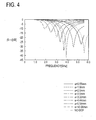
- FIG. 4 shows the measurement result.
- table 1 there is indicated the relation between matching frequency fo and maximum electromagnetic wave absorption.
- the matching frequency fo basically lowers to its low frequency level and the maximum electromagnetic wave absorption lowers.
- the maximum electromagnetic wave absorption is 42.8 dB, the largest maximum absorption amount.
- the electromagnetic wave absorber sheet 1 subject to measurement is configured as: 4 ⁇ 4 array of the conductive films 11 of the DCF 2; 4.6 mm of 'a' for each side's length of conductive films 11; and 1.0 mm of thickness for each conductive film 11.
- electromagnetic wave absorption obtained by changing arrangement distance 'b' of adjoining conductive films 11 within a range of 0.01 mm and 4.6 mm there has been measured electromagnetic wave absorption obtained when DCF 2 is not employed has been measured.
- FIG. 5 shows the measurement result.
- Table 2 there is indicated the relation between matching frequency fo and maximum electromagnetic wave absorption.
- [Table 2] b [mm] Max Absorption [dB] Fo [GHz] 0.01 2.68 0.52 0.1 6.91 1.26 0.5 14.4 2.42 1.5 18.9 3.08 3 26.3 3.7 4.6 34 4.28 No DCF 37.3 5.6
- the matching frequency fo basically lowers to its low frequency level and the maximum electromagnetic wave absorption lowers.
- the electromagnetic wave absorber sheet 1 subject to measurement is configured as: 4 X 4 array of the conductive films 11 of the DCF 2; and 1.0 mm thickness for each conductive film 11.
- arrangement distance-'b'-of-adjoining conductive films 11 is fixed with the following four different distance of 0.2 mm, 0.5 mm, 1.0 mm and 1.5 mm.
- FIG. 6 shows the measurement result.
- each side's length 'a' of the conductive films 11 when providing maximum electromagnetic wave absorption is longer.
- maximum electromagnetic wave absorption is larger.
- the graph of FIG. 6 indicates that 20 dB or larger, sufficient as electromagnetic wave absorption, can be achieved by properly setting the range of each side's length 'a' of the conductive films 11 and that of arrangement distance 'b' of adjoining conductive films 11.
- each side's length 'a' of the conductive films 11 to a range of 0.5 mm and 4.8 mm and setting arrangement distance 'b' of adjoining conductive films 11 to a range of 0.01 mm and 3 mm, 20 dB or higher of electromagnetic wave absorption can be achieved.
- 8.28 mm of thickness is required of the dielectric layer 3 so as to achieve 2.96 GHz of matching frequency. Accordingly, the measurement result in FIG.
- dispersion treatment is carried out wherein 100 parts (by weight, similarly indicated hereinafter) of carbon black (BF-5AK manufactured by Chuetsu Graphite Works Co., Ltd.), 1 part of PGM (solvent, manufactured by Taiyou Kagaku Co., Ltd.) and 700 parts of Plysurf A212 (dispersant, manufactured by Dai-ichi Kogyo Seiyaku Co., Ltd.) are dispersed by a bead mill (APEX MILL manufactured by Kotobuki Industries Co., Ltd.). It is to be noted that the dispersion treatment conditions are the use of 6 kilograms of bead, 700 rotations per minute and processing speed of 0.1 hr / kg.
- the dispersion liquid obtained at the dispersion treatment is mixed with PMMA solution.
- the mixing ratio is 901 parts of the dispersion liquid, 500 parts of Delpet SR8500 (PMMA resin manufactured by Asahi Kasei Corporation), 1600 parts of toluol (solvent) and 400 parts of MEK (solvent).
- mixed solution is applied to a PET film (75 ⁇ m thick).
- the PET film coated with the mixed solution is dried. It is to be noted that the coating process is carried out under the conditions of 200 ⁇ m of coating thickness, 130 degrees in centigrade of drying temperature and 3 minutes of drying time.
- the DCF 2 is formed by arranging a pattern of the copper foil conductive films 11 on the PI film 12 by means of deposition, etching or printing.
- the PI film 12 with the conductive films 11 being arranged thereon (i.e., the DCF 2) is pasted on one side of the dielectric layer 3 by means of thermal press. Further, an aluminum foil (the electromagnetic wave reflective layer 4) is adhered to the other side of the dielectric layer 3 by adhesive agent or the like. Further on, 30 ⁇ m thickness of an acrylic pressure sensitive adhesive layer formed on a separator is applied to the surface of the aluminum foil, whereby the electromagnetic wave absorber sheet 1 is completed. Additionally, 20 ⁇ m thickness of a fluorinated polymer film is pasted on the top surface of the DCF 2 as protection film 7 by means of thermal press.
- dielectric layer 3 with the four kinds of the dielectric layers 3 difference in complex relative permittivity ⁇ r, there are further combined varieties of thickness 'd' for the electromagnetic wave absorber sheets 1 and those of conductive films 11 to be arrayed for the DCF 2 made different in each side's length 'a' and arrangement distance 'b' of adjoining conductive films 11.
- thickness 'd' for the electromagnetic wave absorber sheets 1 and those of conductive films 11 to be arrayed for the DCF 2 made different in each side's length 'a' and arrangement distance 'b' of adjoining conductive films 11.
- the evaluations results of the first through fourth embodiments indicate that sufficient electromagnetic wave absorption (e.g., 20 dB or higher) can be achieved by setting each side's length 'a' of the conductive films 11 and arrangement distance 'b' of adjoining conductive films 11 to a range of 0.5 mm and 4.8 mm and a range of 0.01 mm and 3 mm, respectively even though the electromagnetic wave absorber sheet 1 has thickness within a range of 0.517 mm and 1.55 mm.
- the electromagnetic wave absorber sheet 1 of the present invention includes the DCF 2, the dielectric layer 3 and the electromagnetic wave reflective layer 4.
- a ratio of 'd', thickness of the electromagnetic wave absorber sheet 1, and ' ⁇ ', wavelength of an electromagnetic wave absorbed by the electromagnetic wave absorber sheet 1 satisfies a range of: 0.01 ⁇ d/ ⁇ ⁇ 0.03, and weight per unit area of the electromagnetic wave absorber sheet 1 falls within a range of 1000 g/m 2 and 3000 g/m 2 .
- the electromagnetic wave absorber sheet 1 employing the DCF 2 can achieve the reduction in film thickness and weight for both the dielectric layer 3 and the DCF 2 while exhibiting sufficient electromagnetic wave absorption property.
- the reduction in film thickness and weight can facilitate pasting of the electromagnetic wave absorber sheet 1 on a wall and a ceiling and significantly increase chances of using the electromagnetic wave absorber sheet 1. Further, the reduction in film thickness for the electromagnetic wave absorber sheet 1 helps lower matching frequency to its lower frequency level.
- the DCF 2 is constituted by arranging a plurality of conductive films 11 at predetermined distance, wherein each side's length of the conductive films 11 is dimensioned within a range of 0.5 mm and 4.8 mm and the predetermined distance between adjoining conductive films 11 is within a range of 0.01 mm and 3 mm. Accordingly, the electromagnetic wave absorber sheet 1 employing the DCF 2 can achieve reduction in film thickness and weight for both the dielectric layer 3 and the DCF 2 while exhibiting sufficient electromagnetic wave absorption property.
- the dielectric layer 3 is a layer made of thermoplastic material in which flake graphite is dispersed and arrayed vertically with reference to an incident direction of an electromagnetic wave. Accordingly, flat faces of flake graphite can be laid vertically with reference to the incident direction of an electromagnetic wave, which enables the dielectric layer 3 to increase a real part value of its complex relative permittivity without increasing an imaginary part significantly. Consequently, this enables the electromagnetic wave absorber sheet 1 to raise the complex relative permittivity to its higher level and to meet a non-reflecting state. Thereby, the electromagnetic wave absorber sheet 1 can achieve reduction in film thickness and weight.
- complex relative permittivity consisting of a real part and an imaginary part, of the dielectric layer 3 satisfies conditions such that: the real part falls within a range between 10 and 40; and a numerical value portion of the imaginary part falls within a range between 2 and 8.
- a real part and an imaginary part of all-inclusive complex relative permittivity of the electromagnetic wave absorber sheet 1 inclusive of the dielectric layer 3 and the DCF 2 satisfies a non-reflecting condition and the real part and the imaginary part of the complex relative permittivity of the dielectric layer 3 are respectively smaller than the real part and the imaginary part of the all-inclusive complex relative permittivity. Accordingly, the electromagnetic wave absorber sheet 1 incorporating the DCF 2 and the dielectric layer 3 therein can be designed to meet non-reflecting condition. Thereby, an electromagnetic wave coming in the electromagnetic wave absorber sheet 1 can be attenuated.
- the conductive films 11 mounted on the DCF 2 are shaped into square, however, they may be shaped into other forms (e.g., rectangular).
- Flake graphite is used as electromagnetic wave absorber material to be dispersed in the dielectric layer 3 in the present embodiment, however, other carbonic material, metallic material, ceramic material may be used.
Landscapes
- Physics & Mathematics (AREA)
- Electromagnetism (AREA)
- Engineering & Computer Science (AREA)
- Microelectronics & Electronic Packaging (AREA)
- Shielding Devices Or Components To Electric Or Magnetic Fields (AREA)
- Laminated Bodies (AREA)
Abstract
Description
- The present invention relates to an electromagnetic wave absorber that absorbs electromagnetic waves radiated from electronic components such as motor, etc.
- There have recently seen occasional erroneous operations in electronic components due to electromagnetic disturbances of electronic components such as motor, computer, etc. What is worse, radiation of electromagnetic waves has been known as unfavorable influence upon the human body. To avoid the unfavorable influence of electromagnetic wave radiation, there have been used electromagnetic wave absorbers for absorbing electromagnetic waves. Specifically, electromagnetic wave absorbers have been applied to wall portions surrounding electronic components that radiate electromagnetic waves as well as building walls in order to absorb electromagnetic waves radiated from electronic components.
- Incidentally, reduction in film thickness and weight has been required of electromagnetic wave absorbers. For instance, regarding the ETC system (electronic toll collection system) used at toll gates of expressways, employment of electromagnetic wave absorbers have been essential to ceilings and walls of toll gate in order to prevent erroneous operation of an on-vehicle ETC body due to electromagnetic disturbances from adjoining lanes. Therefore, the reduction in film thickness and weight is required of electromagnetic wave absorbers.
- As an example of a conventional electromagnetic wave absorber, there has been used a so-called λ/4 type electromagnetic wave absorber of which configuration is designed based on a non-reflecting condition expression that makes electromagnetic waves non-reflective at a surface of the electromagnetic wave absorber.
- The λ/4 type electromagnetic wave absorber includes a dielectric layer with a thickness of λ/(4· √ εr) and a relative permittivity of εr (λ representing wavelength of electromagnetic wave in a vacuum state, er representing relative permittivity of the dielectric). One surface of the dielectric layer includes an electromagnetic wave reflective layer and the other surface thereof includes an electrical resistance film layer with an electric-wave impedance of 377Ω in the air. In this connection, the dielectric layer of the λ/4 type electromagnetic wave absorber needs at least the thickness of λ/(4· √ εr), which restricts degree of reduction in film thickness.
- In recent years, there has been proposed an electromagnetic wave absorber of which dielectric layer thickness is made thinner than λ/(4· √ εr) by inserting a DCF (divided conductive film) between an electrical-resistance film and a reflective layer of a λ/4 type electromagnetic wave absorber (for instance, refer to
JP Laid-open Patent Application Publication No. 2004-319788 - However, despite insertion of the DCF (divided conductive film) disclosed in Publication No.
2004-319788 2004-319788 - The present invention has been made to solve the above described problem and the object thereof is to provide an electromagnetic wave absorber achieving reduction in film thickness and weight for both a dielectric layer and a DFC (divided conductive film) thereof.
- In order to achieve the above object, according a first aspect of the present invention, there is provided an electromagnetic wave absorber comprising: a dielectric layer; a divided conductive film layer laminated on one surface of the dielectric layer; and an electromagnetic wave reflective layer laminated on other surface of the dielectric layer, wherein a ratio of 'd', thickness of the electromagnetic wave absorber, and 'λ', wavelength of an electromagnetic wave absorbed by the electromagnetic wave absorber, satisfies a range of : 0.01 ≦ d/λ ≦ 0.03, and wherein weight per unit area of the electromagnetic wave absorber falls within a range of 1000 g/m2 and 3000 g/m2.
- According to the above described electromagnetic wave absorber, the electromagnetic wave absorber employing the DCF can achieve reduction in film thickness and weight for both the dielectric layer and the DCF while exhibiting sufficient electromagnetic wave absorption property. Therefore, the reduction in film thickness and weight can facilitate pasting of the electromagnetic wave absorber on a wall or a ceiling and significantly increase chances of using the electromagnetic wave absorber. Further, the reduction in film thickness for the electromagnetic wave absorber helps lower matching frequency to its lower frequency level. It is to be noted that matching frequency corresponds to frequency of an electromagnetic wave to be absorbed when an electromagnetic wave absorber exhibits its maximum absorption ability.
- According to a second aspect of the present invention, there is provided an electromagnetic wave absorber, wherein the divided conductive film layer is constituted by arranging a plurality of quadrilateral conductive films at predetermined distance, wherein each side's length of the quadrilateral conductive films is dimensioned within a range of 0.5 mm and 4.8 mm, and wherein the predetermined distance between adjoining quadrilateral conductive films is within a range of 0.01 mm and 3 mm.
- According to the above described electromagnetic wave absorber, each side's length of the conductive films and arrangement distance of adjoining conductive films are properly adjusted as parameters of the DCF. Thereby, reduction in film thickness and weight for both the dielectric layer and DCF can be achieved while sufficient electromagnetic wave absorption property is exhibited.
- According to a third aspect of the present invention, there is provided an electromagnetic wave absorber, wherein the dielectric layer is a layer made of thermoplastic resin in which electromagnetic wave absorber material is dispersed.
- According to the above described electromagnetic wave absorber, the dielectric layer is a layer made of thermoplastic resin in which electromagnetic wave absorber material is dispersed. Accordingly, effective permittivity of the dielectric layer can be raised. Consequently, the dielectric layer can achieve reduction in film thickness and weight.
- According to a fourth aspect of the present invention, there is provided an electromagnetic wave absorber, wherein the dielectric layer is a layer made of thermoplastic material in which flake graphite is dispersed and arrayed vertically with reference to an incident direction of an electromagnetic wave.
- According to the above described electromagnetic wave absorber, the dielectric layer is a layer made of thermoplastic material in which flake graphite is dispersed and arrayed vertically with reference to an incident direction of an electromagnetic wave. Accordingly, flat faces of flake graphite can be laid vertically with reference to the incident direction of an electromagnetic wave, which enables the dielectric layer to increase its real part value of the complex relative permittivity without increasing its imaginary part significantly. Consequently, this enables the electromagnetic wave absorber to raise the complex relative permittivity to its higher permittivity level and to meet a non-reflecting state. Thereby, the electromagnetic wave absorber can achieve reduction in film thickness and weight.
- According to a fifth aspect of the present invention, there is provided an electromagnetic wave absorber, wherein complex relative permittivity, consisting of a real part and an imaginary part, of the dielectric layer satisfies conditions such that: the real part falls within a range between 10 and 40; and a numerical value portion of the imaginary part falls within a range between 2 and 8, wherein a real part and an imaginary part of all-inclusive complex relative permittivity of the electromagnetic wave absorber inclusive of the dielectric layer and the divided conductive film layer satisfies a non-reflecting condition, and wherein the real part and the imaginary part of the complex relative permittivity of the dielectric layer are respectively smaller than the real part and the imaginary part of the all-inclusive complex relative permittivity.
- According to the above described electromagnetic wave absorber, the electromagnetic wave absorber incorporating the DCF and the dielectric layer therein can be designed to meet a non-reflecting condition. Thereby, an electromagnetic wave coming in the electromagnetic wave absorber can be attenuated.
-
FIG. 1 is an explanatory view of an electromagnetic wave absorber sheet according to the present invention; -
FIG. 2 is a view showing configuration of a DCF formed in the electromagnetic wave absorber sheet according to the present invention; -
FIG. 3 is a view showing a non-reflecting curve to meet a non-reflecting state and a chart of complex relative permittivity εr of a dielectric layer used in the present embodiment; -
FIG. 4 is a graph showing relation between 'a', each side's length of conductive films of the DCF, and electromagnetic wave absorption characteristics; -
FIG. 5 is a graph showing relation between 'b', arrangement distance of adjoining conductive films of the DCF, and electromagnetic wave absorption characteristics; -
FIG. 6 is a graph showing relation between 'a', each side's length of the conductive films of the DCF, and 'b', arrangement distance of adjoining conductive films; -
FIG. 7 is a chart showing particular combinations of 'a' and 'b' (respectively representing each side's length of the conductive films and arrangement distance of adjoining conductive films) that achieve 20 dB or larger of electromagnetic wave absorption as well as a measurement result of matching frequency fo; -
FIG. 8 is a chart showing particular combinations of 'a' and 'b' (respectively representing each side's length of the conductive films and arrangement distance of adjoining conductive films) that achieve 20 dB or larger of maximum electromagnetic wave absorption when using an electromagnetic wave absorber sheet employing a dielectric layer of which complex relative permittivity εr meets εr = 10 - j2; -
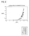
FIG. 9 is a chart showing particular combinations of 'a' and 'b' (respectively representing each side's length of the conductive films and arrangement distance of adjoining conductive films) that achieve 20 dB or larger of maximum electromagnetic wave absorption when using an electromagnetic wave absorber sheet employing a dielectric layer of which complex relative permittivity er meets εr = 20 - j2; -
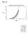
FIG. 10 is a chart showing particular combinations of 'a' and 'b' (respectively representing each side's length of the conductive films and arrangement distance of adjoining conductive films) that achieve 20 dB or larger of maximum electromagnetic wave absorption when using an electromagnetic wave absorber sheet employing a dielectric layer of which complex relative permittivity er meets εr = 30 - j4; and -
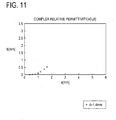
FIG. 11 is a chart showing particular combinations of 'a' and 'b' (respectively representing each side's length of the conductive films and arrangement distance of adjoining conductive films) that achieve 20 dB or larger of maximum electromagnetic wave absorption when using an electromagnetic wave absorber sheet employing a dielectric layer of which complex relative permittivity εr meets εr = 40 - j8. - Here will be described on exemplary embodiments of electromagnetic wave absorbers of the present invention in detail while referring to the drawings.
- First, by referring to
FIG. 1 , there will be described on configuration of an electromagneticwave absorber sheet 1 as example of an electromagnetic wave absorber directed to the present invention.FIG. 1 is an explanatory view of an electromagnetic wave absorber sheet according to the present invention. - As shown in
FIG. 1 , the electromagneticwave absorber sheet 1 essentially consists of a divided conductive film (abbreviated as DCF, hereinafter) 2, adielectric layer 3 and an electromagnetic wavereflective layer 4. Specifically, with reference to an incident direction of an electromagnetic wave, the above mentioned constituent layers are laminated in the order of DCF2, thedielectric layer 3 and the electromagnetic wavereflective layer 4. Further,FIG. 1 shows an exemplary state that the electromagneticwave absorber sheet 1 is adhered to anadherend 5 such as wall or the like with the aid of anadhesive layer 6. Further, a front side of the DCF 2 is coated with a protective film such as fluorinated polymer film or the like exhibiting excellent weather resistance property and heat resistance property. - The
DCF 2 has periodic structure where square-shapedconductive films 11 made of conductive material (e.g., copper foil) are arrayed at equal spaces.FIG. 2 exemplarily shows configuration of theDCF 2. - As shown in
FIG. 2 , theDCF 2 of the present invention is constituted by arranging a plurality of copper foilconductive films 11 on a PI (polyimide)film 12 wherein each side of theconductive films 11 has length 'a' and adjoiningconductive films 11 are arranged at equal distance 'b'. Further, it is preferable that 'a', each side's length of theconductive films 11, is dimensioned within a range of 0.5 mm and 4.8 mm and that 'b', arrangement distance of adjoiningconductive films 11 is taken within a range of 0.01 mm and 3 mm. By arranging 'a' and 'b' within their respective favorable ranges, the inventive electromagnetic wave absorber can achieve reduction in film thickness and weight, in comparison with the conventional λ/4 type electromagnetic wave absorber. - When an electromagnetic wave vertically comes in the
DCF 2, current flows at edge portions of theconductive films 11 and electric fields are collected at gap portions (spaces formed between adjoining conductive films 11). More specifically, a phase delays so as to significantly increase effective permittivity of the electromagnetic wave absorber sheet 1 (also increase a real part and an imaginary part of complex relative permittivity). Accordingly, the electromagneticwave absorber sheet 1 employing theDCF 2 can achieve reduction in film thickness and weight, in comparison with the conventional λ/4 type electromagnetic wave absorber. Further, the reduction in film thickness enables the electromagneticwave absorber sheet 1 to lower its matching frequency to lower frequency level. - It is to be noted that material for the
conductive films 11 of theDCF 2 is not restricted to copper foil but it may be aluminum, gold, silver, or other electrically conductive film material, etc. Theconductive films 11 may be directly mounted on thedielectric layer 3 without intervention of thePI film 12. - The
dielectric layer 3 is formed of thermoplastic resin in which electromagnetic wave absorber material is dispersed. As specific examples of thermoplastic resin for thedielectric layer 3, there may be used polymethylmethacrylate resin (PMMA), polyvinyl butyral (PVB), polyethylene (PE), polyethylene terephthalate (PET), etc. The resin material, however, is not particularly restricted to the above examples as long as it is material that can be cast into a film. Further, as specific examples of electromagnetic wave absorber material, there may be used ceramic material, carbonic material, or metallic material, etc. (particularly, barium titanate, ferrite, etc. may be examples of ceramic material; carbon black, graphite, carbon fiber, etc. may be those of carbonic material; and aluminum, nickel, copper, etc. may be those of metallic material; electromagnetic wave absorber material, however, is not restricted to above particular specified material). Meanwhile, as will be described later, in the present invention, anisotropic flake graphite is used as specific electromagnetic wave absorber material. As material of thermoplastic resin to be used for thedielectric layer 3, material adhesive to both the electromagnetic wavereflective layer 4 and thePI film 12 is used. - In the
dielectric layer 3 of the present invention, flake graphite is dispersed and arrayed vertically with reference to the incident direction of an electromagnetic wave. Accordingly, flat faces of flake graphite can be laid vertically with reference to the incident direction of an electromagnetic wave, which enables the electromagneticwave absorber sheet 1 to increase a real part value of its complex relative permittivity without increasing an imaginary part thereof significantly. Consequently, this enables the electromagneticwave absorber sheet 1 to raise the complex relative permittivity to its higher level and to meet a non-reflecting state. Thereby, the electromagneticwave absorber sheet 1 can achieve reduction in film thickness and weight. - It is preferable that, in the case of the present invention, the complex relative permittivity of the
dielectric layer 3, consisting of a real part and an imaginary part, satisfies conditions such that: the real part falls within a range between 10 and 40; and a numerical value portion of the imaginary part falls within a range between 2 and 8. Further, with reference to an identical value of the real part within the range between 10 and 40, a numerical value part of the imaginary part coupled with the identical value of the real part when satisfying the complex relative permittivity of thedielectric layer 3 is smaller than a numerical value part of the imaginary part coupled with the identical value of the real part when satisfying a non-reflecting condition. That is, a real part and a imaginary part of all-inclusive complex relative permittivity of the electromagneticwave absorber sheet 1 satisfies a non-reflecting condition, and the real part and the imaginary part of the complex relative permittivity of thedielectric layer 3 are respectively smaller than the real part and the imaginary part of the all-inclusive complex relative permittivity. Specifically, arrangement of the above-describedDCF 2 raises the effective permittivity (i.e., raises both a real part and an imaginary part of the complex relative permittivity) of the electromagneticwave absorber sheet 1. Therefore, it is necessary to previously set the effective permittivity of thedielectric layer 3 of its own at low level (i.e. with respect to the complex relative permittivity of thedielectric layer 3, it is necessary to set both a real part and an imaginary part thereof lower than the real part and the imaginary part thereof that meets a non-reflecting state as single body) so that the electromagneticwave absorber sheet 1 incorporating theDCF 2 and thedielectric layer 3 therein shall meet the non-reflecting state. - For instance, in the case of the present invention, the complex relative permittivity εr is settled as any one of followings: εr = 10 - j2; εr = 20 - j2; εr = 30 - j4; or εr = 40 - j8.
FIG. 3 is a view showing a non-reflecting curve to meet a non-reflecting state and a chart of complex relative permittivity εr of thedielectric layer 3 used in the present embodiment. As shown inFIG. 3 , each of the above settled complex relative permittivity εr of thedielectric layer 3 as single body locates under the non-reflecting curve. That is, with reference to an identical value of the real part, a numerical value part of the imaginary part coupled with the identical value of the real part when satisfying the complex relative permittivity of the dielectric layer is smaller than a numerical value part of the imaginary part coupled with the identical value of the real part when satisfying a non-reflecting condition. With respect to the entirety of the electromagneticwave absorber sheet 1 incorporating theDCF 2 and thedielectric layer 3 therein, each complex relative permittivity εr as the entirety thereof moves up and gets on the non-reflecting curve. That is, a real part and a imaginary part of all-inclusive complex relative permittivity of the electromagneticwave absorber sheet 1 satisfies a non-reflecting condition, and the real part and the imaginary part of the complex relative permittivity of thedielectric layer 3 are respectively smaller than the real part and the imaginary part of the all-inclusive complex relative permittivity. - Meanwhile, the electromagnetic wave
reflective layer 4 is a layer serving as reflective means for reflecting an incoming electromagnetic wave. Further, the electromagnetic wavereflective layer 4 is formed from a metallic plate that is made of aluminum, copper, iron, stainless, etc., or from a thin polymer film that is vacuum-sprayed or plated with the above-mentioned metallic material or from a resin film that is reinforced with conductive material such as carbon fiber, etc. Thedielectric layer 3 and the electromagnetic wavereflective layer 4 are laminated by direct thermal adhesion or adhesive agent that is weak enough to avoid serious influence on electromagnetic wave absorption characteristics. Further, the lamination order to constitute the electromagneticwave absorber sheet 1 is designed such that the electromagnetic wavereflective layer 4 is laminated behind thedielectric layer 3 with reference to the incident direction side where an electromagnetic wave comes in.FIG. 1 shows that the incident direction of an electromagnetic wave is in vertical with reference to the electromagnetic wavereflective layer 4, however, the incident direction may not be in vertical with reference to the electromagnetic wavereflective layer 4. - The electromagnetic
wave absorber sheet 1 of the present invention may include theadhesive layer 6, if necessary, so as to get thesheet 1 adhered to theadherend 5. Theadhesive layer 6 may be made of proper adhesive agent, however, it may be more preferable that theadhesive layer 6 is made of a pressure-sensitive adhesion layer for simple and quick pasting operation. Specifically, proper pressure-sensitive adhesion material may be used for it. Generally, for instance, there may be used organic series, such as: rubber pressure sensitive adhesive; acrylic pressure sensitive adhesive; silicone pressure sensitive adhesive; vinyl alkyl ether pressure sensitive adhesive; polyvinyl alcohol pressure sensitive adhesive; polyvinyl pyrrolidone pressure sensitive adhesive; polyacrylamide pressure sensitive adhesive; cellulose pressure sensitive adhesive, etc. - Further, the
adhesive layer 6 may be applied at any proper stages before the final stage of pasting the electromagneticwave absorber sheet 1 on theadherend 5. Accordingly, theadhesibe layer 6 may be previously applied to the electromagneticwave absorber sheet 1 in the course of manufacturing thereof or may be applied to the electromagneticwave absorber sheet 1 as end product. - The
adhesive layer 6 may be applied to the electromagneticwave absorber sheet 1 in accordance with: rolling method such as calendar roll method or the like; sheet formation method such as doctor blade method or gravure roll coater method so as to properly add adhesive material to the electromagneticwave absorber sheet 1; or method where theadhesive layer 6 formed in accordance with any of the afore-mentioned methods is adhered to the electromagneticwave absorber sheet 1 at the one side and covered with a separator at the other side. - Thickness of the
adhesive layer 6 may be arbitrarily determined, generally between 1 µm and 500 µm, depending on the intended use. In case the thus arrangedadhesive layer 6 is exposed, the exposed side of theadhesive layer 6 may be covered with a separator or the like so to avoid adhesion of dust thereto and the like, if necessary, until getting adhered to theadherend 5. - The
protection film 7 is formed of: a film made from fluorinated resin, more specifically, fluorinated polymer; a coated layer; and an impregration film. Material of fluorinated polymer to be used for making up theprotection film 7 is not restricted to particular one but proper material may be used depending on desired characteristics. For instance, there may be used polytetrafluoroethylene, and tetrafluoroethylene-perfluoroalkyl vinyl ether copolymer, tetrafluoroethylene-hexafluoropropylene copolymer, and ethylene-tetrafluoroethylene copolymer, polychlorotrifluoroethylene (PCTFE) and ethylene chlorotrifluoroethylene copolymer (ECTFE), polyvinylidene fluoride (PVDF) and polyvinyl fluoride (PVF). The above-exemplified fluorinated polymer exhibits excellent environmental resistance properties such as ozone resistance, weather resistance, heat resistance, etc. Further, plural kinds of above-exemplified fluorinated polymer may be mixed and used. Further, reinforce base material such as fiber, etc. may be mixed in theprotection film 7, as necessary. - Alternatively, the
protection film 7 may be formed by mixing fluorinated polymer and non-fluorinated polymer in order to improve physical properties thereof. Mixing balance of non-fluorinated polymer should be 80 % by weight or lower of fluorinated polymer or lower, preferably, 50 % by weight or lower, or more preferably, 20 % by weight or lower in order to maintain weather resistance, etc. - It is preferable that thickness of the
protection film 7 is 0.1 µm or thicker in view of intensity, weather resistance, etc. For instance, 20 µm thick may be proper. - It is favorable to use the above-described electromagnetic
wave absorber sheet 1 of the present invention as measure against radiation of electromagnetic wave at buildings such as toll gate of ETC (electric toll collecting system), gas station, etc., vehicle safety fences such as guardrail, high-rise buildings, etc. Especially, arrangement of theprotection film 7 enhances weather resistance property and rubfastness of the electromagnetic wave absorber sheet. Accordingly, the inventive electromagnetic wave absorber sheet with such protection film is favorably applied to things to be exposed open air when being used. - Further, the electromagnetic
wave absorber sheet 1 of the present invention includes the above-describedDCF 2. Further, each side's length 'a' of theconductive films 11 and arrangement distance 'b' of adjoiningconductive films 11 are properly adjusted as parameters of theDCF 2 so that the reduction in film thickness and weight for the electromagneticwave absorber sheet 1 can be achieved. In consideration of the case where the electromagneticwave absorber sheet 1 is pasted on a wall or a ceiling, it is preferable that a ratio of 'd', thickness of the electromagneticwave absorber sheet 1 incorporating theDCF 2, thedielectric layer 3 and the electromagnetic wavereflective layer 4 therein, and 'λ', wavelength of an electromagnetic wave absorbed by the electromagneticwave absorber sheet 1, satisfies: 0.01 ≦d/λ ≦ 0.03. Further, it is also preferable that weight per unit area of the electromagneticwave absorber sheet 1 falls within a range of 1000 g/m2 and 3000 g/m2 - Here will be described on the relation of 'a' and 'b' (respectively representing each side's length of the
conductive films 11 and arrangement distance of adjoining conductive films 11) and electromagnetic wave absorption characteristics. It is to be noted theconductive films 11 constitutes theDCF 2 used for the electromagneticwave absorber sheet 1. - In the below described example, with respect to
dielectric layer 3 of the electromagneticwave absorber sheet 1, its complex relative permittivity is set as (er = 9.53 - j3.72) and thickness as 4.43 mm. With the above-mentioned fixed settings, change of matching frequency fo and that of electromagnetic wave absorption are measured by changing each side's length 'a' of theconductive films 11 and arrangement distance 'b' of adjoiningconductive films 11. - The electromagnetic
wave absorber sheet 1 subject to measurement is configured as: 4X 4 array of theconductive films 11 of theDCF 2; 1mm of arrangement distance 'b' between adjoiningconductive films 11; and 1.0 mm thickness for eachconductive film 11. With the above fixed configuration, there has been measured electromagnetic wave absorption obtained by changing each side's length 'a' of theconductive films 11 within a range of 0.55 mm and 10.06 mm. Also, as comparative example thereof, electromagnetic wave absorption obtained whenDCF 2 is not employed has been measured.FIG. 4 shows the measurement result. In table 1, there is indicated the relation between matching frequency fo and maximum electromagnetic wave absorption.[Table 1] a [mm] Max Absorption [dB] Fo [GHz] 0.55 27.7 5.32 1.8 30.9 4.6 2 42.8 3.92 2.5 34.5 3.7 3.33 24.8 3.36 4.44 19.6 3.04 5.54 14.1 2.48 10.06 10.3 1.92 No DCF 37.3 5.6 - As shown in
FIG. 4 and table 1, as the each side's length 'a' is made longer, the matching frequency fo basically lowers to its low frequency level and the maximum electromagnetic wave absorption lowers. When 'a' is set to 2.0 mm, the maximum electromagnetic wave absorption is 42.8 dB, the largest maximum absorption amount. - Here, the electromagnetic
wave absorber sheet 1 subject to measurement is configured as: 4 × 4 array of theconductive films 11 of theDCF 2; 4.6 mm of 'a' for each side's length ofconductive films 11; and 1.0 mm of thickness for eachconductive film 11. With the above fixed configuration, there has been measured electromagnetic wave absorption obtained by changing arrangement distance 'b' of adjoiningconductive films 11 within a range of 0.01 mm and 4.6 mm. Also, as comparative example thereof, electromagnetic wave absorption obtained whenDCF 2 is not employed has been measured.FIG. 5 shows the measurement result. In table 2, there is indicated the relation between matching frequency fo and maximum electromagnetic wave absorption.[Table 2] b [mm] Max Absorption [dB] Fo [GHz] 0.01 2.68 0.52 0.1 6.91 1.26 0.5 14.4 2.42 1.5 18.9 3.08 3 26.3 3.7 4.6 34 4.28 No DCF 37.3 5.6 - As shown in
FIG. 5 and table 2, as arrangement distance 'b' of adjoiningconductive films 11 is made shorter, the matching frequency fo basically lowers to its low frequency level and the maximum electromagnetic wave absorption lowers. - Next, four of different arrangement distance 'b' array patterns are prepared with respect to array of the
conductive films 11 of theDCF 2. With respect to each of the four array patterns, there have been measured matching frequency fo and maximum electromagnetic wave absorption obtained by changing side's length 'a' of theconductive films 11. - Here, the electromagnetic
wave absorber sheet 1 subject to measurement is configured as: 4X 4 array of theconductive films 11 of theDCF 2; and 1.0 mm thickness for eachconductive film 11. With the above fixed configuration, arrangement distance-'b'-of-adjoiningconductive films 11 is fixed with the following four different distance of 0.2 mm, 0.5 mm, 1.0 mm and 1.5 mm. With the above four different fixed configuration, there have been measured matching frequency fo and maximum electromagnetic wave absorption obtained by changing each side's length 'a' of theconductive films 11.FIG. 6 shows the measurement result. - As shown in
FIG.6 , as the arrangement distance 'b' of adjoiningconductive films 11 is made longer, each side's length 'a' of theconductive films 11 when providing maximum electromagnetic wave absorption is longer. With the synergy, maximum electromagnetic wave absorption is larger. The graph ofFIG. 6 indicates that 20 dB or larger, sufficient as electromagnetic wave absorption, can be achieved by properly setting the range of each side's length 'a' of theconductive films 11 and that of arrangement distance 'b' of adjoiningconductive films 11. For instance, by setting each side's length 'a' of theconductive films 11 to a range of 0.5 mm and 4.8 mm and setting arrangement distance 'b' of adjoiningconductive films 11 to a range of 0.01 mm and 3 mm, 20 dB or higher of electromagnetic wave absorption can be achieved. - Out of combinations 'a' and 'b' (respectively representing each side's length of the conductive films and arrangement distance of adjoining conductive films) shown in
FIG. 6 , the chart shown inFIG. 7 indicates particular combinations of 'a' and 'b' that achieve 20 dB, or larger of electromagnetic wave absorption as well as a measurement result of matching frequency fo. - As shown in
FIG. 7 , as the arrangement distance 'b' of adjoiningconductive films 11 is made shorter, matching frequency fo of each side's length 'a' of the conductive films 11 (when 'a' is fixed) lowers to its lower frequency level. - As the cause of the above phenomenon, binding of electric fields between adjoining
conductive films 11 can be pointed out. More specifically, concentration of electrical charges at edge portions of theconductive films 11 makes theDCF 2 work as capacitor. Consequently, the matching frequency fo lowers to its lower frequency level. In other words, because capacity of the capacitor gets larger as the arrangement distance 'b' of adjoiningconductive films 11 is made shorter, the matching frequency fo lowers to its lower frequency level as shown inFIG. 7 . - The measurement result shown in
FIG. 7 indicates that 20dB of electromagnetic wave absorption and 2.96 GHz of matching frequency can be achieved when the electromagneticwave absorber sheet 1 subject to measurement employs: thedielectric layers 3 with (εr = 9.53 - j3.72) of complex relative permittivity and 4.43 mm thickness; andconductive films 11 with 2.5 mm of each side's length 'a' for theconductive films 11 and 0.5 mm of arrangement distance 'b' between adjoiningconductive films 11. On the other hand, in case of an electromagnetic wave absorber that incorporates theDCF 2 from which the above specifieddielectric layer 3 is excluded, 8.28 mm of thickness is required of thedielectric layer 3 so as to achieve 2.96 GHz of matching frequency. Accordingly, the measurement result inFIG. 7 indicates that 47 % of reduction in film thickness can be achieved when the inventive electromagneticwave absorber sheet 1 employs theDCF 2 of which parameters 'a' and 'b' (respectively representing each side's length of theconductive films 11 and arrangement distance of adjoining conductive films) are set properly. - Embodiments of the present invention will be described hereinafter.
- Firstly, manufacturing process of the electromagnetic
wave absorber sheet 1 will be described. - First, dispersion treatment is carried out wherein 100 parts (by weight, similarly indicated hereinafter) of carbon black (BF-5AK manufactured by Chuetsu Graphite Works Co., Ltd.), 1 part of PGM (solvent, manufactured by Taiyou Kagaku Co., Ltd.) and 700 parts of Plysurf A212 (dispersant, manufactured by Dai-ichi Kogyo Seiyaku Co., Ltd.) are dispersed by a bead mill (APEX MILL manufactured by Kotobuki Industries Co., Ltd.). It is to be noted that the dispersion treatment conditions are the use of 6 kilograms of bead, 700 rotations per minute and processing speed of 0.1 hr / kg.
- Next, the dispersion liquid obtained at the dispersion treatment is mixed with PMMA solution. The mixing ratio is 901 parts of the dispersion liquid, 500 parts of Delpet SR8500 (PMMA resin manufactured by Asahi Kasei Corporation), 1600 parts of toluol (solvent) and 400 parts of MEK (solvent).
- Thus mixed solution is applied to a PET film (75 µm thick). The PET film coated with the mixed solution is dried. It is to be noted that the coating process is carried out under the conditions of 200 µm of coating thickness, 130 degrees in centigrade of drying temperature and 3 minutes of drying time.
- Thereafter, sheets formed on the PET film are peeled off therefrom and laminated together. Vacuum thermal press is applied to the laminated sheets (under 100 degrees in centigrade and 15 minutes) by using a spacer previously set to predetermined thickness. Thereby, the
electric layer 3 is formed. - Meanwhile, the
DCF 2 is formed by arranging a pattern of the copper foilconductive films 11 on thePI film 12 by means of deposition, etching or printing. - The
PI film 12 with theconductive films 11 being arranged thereon (i.e., the DCF 2) is pasted on one side of thedielectric layer 3 by means of thermal press. Further, an aluminum foil (the electromagnetic wave reflective layer 4) is adhered to the other side of thedielectric layer 3 by adhesive agent or the like. Further on, 30 µm thickness of an acrylic pressure sensitive adhesive layer formed on a separator is applied to the surface of the aluminum foil, whereby the electromagneticwave absorber sheet 1 is completed. Additionally, 20 µm thickness of a fluorinated polymer film is pasted on the top surface of theDCF 2 asprotection film 7 by means of thermal press. - By carrying out the above described manufacturing processes, four kinds of electromagnetic
wave absorber sheets 1 are manufactured. Specifically, the difference of the four kinds of electromagneticwave absorber sheets 1 lies in different complex relative permittivity εr of thedielectric layer 3 employed therein: (first embodiment: εr = 10 - j2); (second embodiment: εr = 20 - j2); (third embodiment: εr = 30 - j4); and (fourth embodiment: εr = 40 - j8). Further, with the four kinds of thedielectric layers 3 difference in complex relative permittivity εr, there are further combined varieties of thickness 'd' for the electromagneticwave absorber sheets 1 and those ofconductive films 11 to be arrayed for theDCF 2 made different in each side's length 'a' and arrangement distance 'b' of adjoiningconductive films 11. By thus combining various thickness,dielectric layer 3 with various complex relative permittivity εr and various patternedconductive films 11, plural electromagneticwave absorber sheets 1 have been prepared for the respective embodiments. - With respect to each of electromagnetic wave absorber sheets prepared for the first embodiment, maximum electromagnetic wave absorption has been measured.
- The below provided table 3 indicates the measurement result of respective electromagnetic wave absorber sheets that have achieved 20 dB or higher of maximum electromagnetic wave absorption by employing the
dielectric layer 3 that meets complex relative permittivity εr of (εr = 10 - j2). Further,FIG. 8 shows the graph corresponding to the table 3.[Table 3] Complex Relative Permittivity: 10 - j2 d [mm] a [mm] b [mm] Max Absorption [dB] 1.1 2.5 0.009 23 2.7 0.012 21 2.9 0.016 20 1.2 2 0.005 21 2.5 0.012 25 2.7 0.017 24 3 0.025 23 3.2 0.035 28 3.5 0.05 23 3.7 0.065 25 3.9 0.085 21 1.3 2 0.007 25 2.5 0.016 32 3 0.035 27 3.2 0.05 22 3.5 0.07 24 3.7 0.09 23 4 0.12 20 4.2 0.17 22 4.5 0.22 22 4.7 0.28 20 5 0.35 21 5.2 0.42 20 5.4 0.5 20 1.4 2 0.01 22 3 0.05 31 3.5 0.09 29 3.7 0.12 29 4 0.15 21 4.2 0.2 24 4.5 0.27 24 4.7 0.32 24 5 0.4 20 5.2 0.5 21 5.4 0.6 21 5.6 0.7 20 5.8 0.85 20 6 1.08 20 - The measurement result shown in table 3 and
FIG. 8 indicates combinations of 'a' and 'b' (respectively representing each side's length ofconductive films 11 and arrangement distance of adjoining conductive films 11) to achieve 20dB or higher of maximum electromagnetic wave absorption when the electromagneticwave absorber sheet 1 that employs thedielectric layer 3 meeting complex relative permittivity εr of (εr = 10 - j2) is configured to have thickness 'd' of 1.1 mm, 1.2 mm, 1.3 mm or 1.4 mm. Especially, combinations of (d = 1.2 mm, a = 3.2 mm, b = 0.035 mm), (d = 1.3 mm, a = 2.5 mm ∼ 3.0 mm, b = 0.016 mm ∼ 0.035 mm) and (d = 1.4 mm, a = 3.0 mm ∼ 3.7 mm, b = 0.056 mm ∼ 0.12 mm) have achieved high maximum electromagnetic wave absorption. - The below provided table 4 indicates the measurement result of respective electromagnetic wave absorber sheets that have achieved 20 dB or higher of maximum electromagnetic wave absorption by employing the
dielectric layer 3 that meets complex relative permittivity εr of (εr = 20 - j2). Further,FIG. 9 shows the graph corresponding to the table 4.

- The measurement result shown in table 4 and
FIG. 9 indicates that combinations of 'a' and 'b' (respectively representing each side's length ofconductive films 11 and arrangement distance of adjoining conductive films 11) to achieve 20dB or higher of maximum electromagnetic wave absorption when the electromagneticwave absorber sheet 1 that employs thedielectric layer 3 meeting complex relative permittivity er of (er = 20 - j2) is configured to have thickness 'd' of 0.7 mm, 0.8 mm, 0.9 mm, 1.0 mm, 1.1 mm or 1.2 mm. Especially, combinations of (d = 0.8 mm, a = 3.0 mm ∼ 3.2 mm, b = 0.06 mm ∼ 0.08 mm), (d = 0.8 mm, a = 3.8 mm ∼ 4.0 mm, b = 0.2 mm ∼ 0.28 mm), (d = 0.9 mm, a = 4.0 mm ∼ 4.2 mm, b = 0.38 mm ∼ 0.50 mm), (d = 1.1 mm, a = 4.7 mm ∼ 4.8 mm, b = 1.8 mm ∼ 2.0 mm) and (d = 1.2 mm, a = 4.8 mm, b = 2.5 mm) have achieved high maximum electromagnetic wave absorption. - The below provided table 5 indicates the measurement result of respective electromagnetic wave absorber sheets that have achieved 20 dB or higher of maximum electromagnetic wave absorption by employing the
dielectric layer 3 that meets complex relative permittivity εr of (εr = 30 - j4). Further,FIG. 10 shows the graph corresponding to the table 5.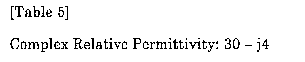

- The measurement result shown in table 5 and
FIG. 10 indicates combinations of 'a' and 'b' (respectively representing each side's length ofconductive films 11 and arrangement distance of adjoining conductive films 11) to achieve 20 dB or higher of maximum electromagnetic wave absorption when the electromagneticwave absorber sheet 1 that employs thedielectric layer 3 meeting complex relative permittivity er of (er = 30 - j4) is configured to have thickness 'd' of 0.9 mm, 1.0 mm, 1.1 mm and 1.2 mm, 1.3 mm and 1.4 mm. Especially, combinations of (d = 1.1 mm, a = 2.3 mm ∼ 2.7 mm, b = 0.225 mm ∼0.4 mm), (d = 1.2 mm, a = 2.8 mm ∼ 3.4 mm, b = 0.6 mm ∼1.3 mm), (d = 1.3 mm, a = 3.1 mm ∼ 3.2 mm, b = 1.1 mm ∼ 1.25 mm) and (d = 1.4 mm, a = 3.4 mm, b = 2 mm) have achieved high maximum electromagnetic wave absorption. - The below provided table 6 indicates the measurement result of respective electromagnetic wave absorber sheet that have achieved 20 dB or higher of maximum electromagnetic wave absorption by employing the
dielectric layer 3 that meets complex relative permittivity εr of (εr = 40 - j8). Further,FIG. 11 shows the graph corresponding to the table 6.[Table 6] Complex Relative Permittivity: 40 - j8 d [mm] a [mm] b [mm] Max Absorption [dB] 1.4 0.4 0.004 22 0.6 0.017 20 0.8 0.005 21 1 0.1 21 1.2 0.2 20 1.5 0.37 20 1.7 0.52 20 - The measurement result shown in table 6 and
FIG. 11 indicates that combinations of 'a' and 'b' (respectively representing each side's length ofconductive films 11 and arrangement distance of adjoining conductive films 11) to achieve 20dB or higher of maximum electromagnetic wave absorption when the electromagneticwave absorber sheet 1 that employs thedielectric layer 3 meeting complex relative permittivity er of (εr = 40 - j8) is configured to have thickness 'd' of 1.4 mm. - The evaluations results of the first through fourth embodiments indicate that sufficient electromagnetic wave absorption (e.g., 20 dB or higher) can be achieved by setting each side's length 'a' of the
conductive films 11 and arrangement distance 'b' of adjoiningconductive films 11 to a range of 0.5 mm and 4.8 mm and a range of 0.01 mm and 3 mm, respectively even though the electromagneticwave absorber sheet 1 has thickness within a range of 0.517 mm and 1.55 mm. - As described in the above, the electromagnetic
wave absorber sheet 1 of the present invention includes theDCF 2, thedielectric layer 3 and the electromagnetic wavereflective layer 4. In the inventive electromagneticwave absorber sheet 1, a ratio of 'd', thickness of the electromagneticwave absorber sheet 1, and 'λ', wavelength of an electromagnetic wave absorbed by the electromagneticwave absorber sheet 1, satisfies a range of: 0.01 ≦ d/λ ≦ 0.03, and weight per unit area of the electromagneticwave absorber sheet 1 falls within a range of 1000 g/m2 and 3000 g/m2. Accordingly, the electromagneticwave absorber sheet 1 employing theDCF 2 can achieve the reduction in film thickness and weight for both thedielectric layer 3 and theDCF 2 while exhibiting sufficient electromagnetic wave absorption property. Therefore, the reduction in film thickness and weight can facilitate pasting of the electromagneticwave absorber sheet 1 on a wall and a ceiling and significantly increase chances of using the electromagneticwave absorber sheet 1. Further, the reduction in film thickness for the electromagneticwave absorber sheet 1 helps lower matching frequency to its lower frequency level. - Further, the
DCF 2 is constituted by arranging a plurality ofconductive films 11 at predetermined distance, wherein each side's length of theconductive films 11 is dimensioned within a range of 0.5 mm and 4.8 mm and the predetermined distance between adjoiningconductive films 11 is within a range of 0.01 mm and 3 mm. Accordingly, the electromagneticwave absorber sheet 1 employing theDCF 2 can achieve reduction in film thickness and weight for both thedielectric layer 3 and theDCF 2 while exhibiting sufficient electromagnetic wave absorption property. - Further, the
dielectric layer 3 is a layer made of thermoplastic material in which flake graphite is dispersed and arrayed vertically with reference to an incident direction of an electromagnetic wave. Accordingly, flat faces of flake graphite can be laid vertically with reference to the incident direction of an electromagnetic wave, which enables thedielectric layer 3 to increase a real part value of its complex relative permittivity without increasing an imaginary part significantly. Consequently, this enables the electromagneticwave absorber sheet 1 to raise the complex relative permittivity to its higher level and to meet a non-reflecting state. Thereby, the electromagneticwave absorber sheet 1 can achieve reduction in film thickness and weight. - Further, complex relative permittivity, consisting of a real part and an imaginary part, of the
dielectric layer 3 satisfies conditions such that: the real part falls within a range between 10 and 40; and a numerical value portion of the imaginary part falls within a range between 2 and 8. Further, a real part and an imaginary part of all-inclusive complex relative permittivity of the electromagneticwave absorber sheet 1 inclusive of thedielectric layer 3 and theDCF 2 satisfies a non-reflecting condition and the real part and the imaginary part of the complex relative permittivity of thedielectric layer 3 are respectively smaller than the real part and the imaginary part of the all-inclusive complex relative permittivity. Accordingly, the electromagneticwave absorber sheet 1 incorporating theDCF 2 and thedielectric layer 3 therein can be designed to meet non-reflecting condition. Thereby, an electromagnetic wave coming in the electromagneticwave absorber sheet 1 can be attenuated. - Not to mention, the present invention is not limited to the above-described embodiment but may be variously improved and modified without departing from the scope of the present invention.
- The
conductive films 11 mounted on theDCF 2 are shaped into square, however, they may be shaped into other forms (e.g., rectangular). - Flake graphite is used as electromagnetic wave absorber material to be dispersed in the
dielectric layer 3 in the present embodiment, however, other carbonic material, metallic material, ceramic material may be used.
Claims (5)
- An electromagnetic wave absorber (1) comprising:a dielectric layer (3);
a divided conductive film layer (2) laminated on one surface of thedielectric layer (3); and
an electromagnetic wave reflective layer (4) laminated on other surface ofthe dielectric layer (3),
wherein a ratio of 'd', thickness of the electromagnetic wave absorber (1), and 'λ', wavelength of an electromagnetic wave absorbed by the electromagnetic wave absorber (1), satisfies a range of : 0.01 ≦ d/λ ≦ 0.03, and
wherein weight per unit area of the electromagnetic wave absorber (1) falls within a range of 1000 g/m2 and 3000 g/m2. - The electromagnetic wave absorber (1) according to claim 1,
wherein the divided conductive film layer (2) is constituted by arranging a plurality of quadrilateral conductive films (11) at predetermined distance,
wherein each side's length of the quadrilateral conductive films (11) is dimensioned within a range of 0.5 mm and 4.8 mm, and
wherein the predetermined distance between adjoining quadrilateral conductive films (11) is within a range of 0.01 mm and 3 mm. - The electromagnetic wave absorber (1) according to claim 1 or 2,
wherein the dielectric layer (3) is a layer made of thermoplastic resin in which electromagnetic wave absorber material is dispersed. - The electromagnetic wave absorber (1) according to claim 3,
wherein the dielectric layer (3) is a layer made of thermoplastic material in which flake graphite is dispersed and arrayed vertically with reference to an direction of an electromagnetic wave. - The electromagnetic wave absorber (1) according to any one of claims 1 through 4,
wherein complex relative permittivity, consisting of a real part and an imaginary part, of the dielectric layer (3) satisfies conditions such that:the real part falls within a range between 10 and 40; anda numerical value portion of the imaginary part falls within a range between 2 and 8,wherein a real part and an imaginary part of all-inclusive complex relative permittivity of the electromagnetic wave absorber (1) inclusive of the dielectric layer (3) and the divided conductive film layer (2) satisfies a non-reflecting condition, andwherein the real part and the imaginary part of the complex relative permittivity of the dielectric layer (3) are respectively smaller than the real part and the imaginary part of the all-inclusive complex relative permittivity.
Applications Claiming Priority (1)
| Application Number | Priority Date | Filing Date | Title |
|---|---|---|---|
| JP2010101268A JP2011233642A (en) | 2010-04-26 | 2010-04-26 | Electromagnetic wave absorber |
Publications (2)
| Publication Number | Publication Date |
|---|---|
| EP2381756A2 true EP2381756A2 (en) | 2011-10-26 |
| EP2381756A3 EP2381756A3 (en) | 2011-12-28 |
Family
ID=44201959
Family Applications (1)
| Application Number | Title | Priority Date | Filing Date |
|---|---|---|---|
| EP11003179A Withdrawn EP2381756A3 (en) | 2010-04-26 | 2011-04-14 | Electromagnetic wave absorber |
Country Status (4)
| Country | Link |
|---|---|
| US (1) | US8643531B2 (en) |
| EP (1) | EP2381756A3 (en) |
| JP (1) | JP2011233642A (en) |
| CN (1) | CN102238860A (en) |
Cited By (4)
| Publication number | Priority date | Publication date | Assignee | Title |
|---|---|---|---|---|
| CN102570049A (en) * | 2012-01-11 | 2012-07-11 | 东南大学 | Graphene-based electromagnetic absorber |
| KR20200006354A (en) * | 2018-07-10 | 2020-01-20 | 한국항공우주산업 주식회사 | Dielectric substance of Resonance Circuit for Broadband Electromagnetic absorption and Pattern of Dielectric substance having the Same and Capacitance Panel for Aircraft having the Same |
| CN113329607A (en) * | 2021-05-31 | 2021-08-31 | 中国人民解放军空军工程大学 | Novel ultra-wideband wave absorbing unit and wave absorbing structure thereof |
| JP2023019268A (en) * | 2021-07-29 | 2023-02-09 | Tdk株式会社 | noise suppression sheet |
Families Citing this family (19)
| Publication number | Priority date | Publication date | Assignee | Title |
|---|---|---|---|---|
| US20130285846A1 (en) * | 2010-12-27 | 2013-10-31 | Seiji Kagawa | Near-field electromagnetic wave absorber |
| KR101337959B1 (en) * | 2012-03-19 | 2013-12-09 | 현대자동차주식회사 | Composite for shielding electromagnetic wave |
| JP6063631B2 (en) * | 2012-03-26 | 2017-01-18 | 日東電工株式会社 | Electromagnetic wave absorber and method for producing electromagnetic wave absorber |
| DE102012105650B4 (en) * | 2012-06-27 | 2014-09-18 | Avl Trimerics Gmbh | Device for improving the electromagnetic compatibility of electrically operated components used in a motor vehicle |
| US9356357B2 (en) * | 2013-01-11 | 2016-05-31 | Sabic Global Technologies B.V. | Methods and compositions for destructive interference |
| US9252496B2 (en) * | 2013-01-11 | 2016-02-02 | Sabic Global Technologies B.V. | Methods and compositions for energy dissipation |
| PL413567A1 (en) * | 2015-08-14 | 2017-02-27 | Uniwersytet Wrocławski | Free space absorber |
| CN106332536B (en) * | 2016-08-26 | 2019-08-02 | 京东方科技集团股份有限公司 | An electromagnetic interference shielding structure |
| CN106760001B (en) * | 2016-11-23 | 2019-07-19 | 中国建筑材料科学研究总院 | Outer wall structure of building |
| JP7162414B2 (en) * | 2017-06-13 | 2022-10-28 | 日東電工株式会社 | Electromagnetic wave absorbers and molded products with electromagnetic wave absorbers |
| JP7117084B2 (en) * | 2017-06-13 | 2022-08-12 | 日東電工株式会社 | Electromagnetic wave absorbers and molded products with electromagnetic wave absorbers |
| CN109066096A (en) * | 2018-07-24 | 2018-12-21 | 南京邮电大学 | A kind of THz ultra wide band wave absorbing device based on unequal spacing stepped construction |
| CN108901194B (en) * | 2018-08-14 | 2024-07-23 | 桂林电子科技大学 | A new type of ultra-wideband absorber |
| RU189944U1 (en) * | 2018-12-11 | 2019-06-11 | Государственное Унитарное Предприятие Республики Крым "Конструкторско-Технологическое Бюро "Судокомпозит" | ELECTROMAGNETIC WAVE ABSORBENT |
| JP7091469B2 (en) * | 2019-06-07 | 2022-06-27 | 日東電工株式会社 | Radio wave absorbing member, radio wave absorbing structure, and inspection equipment |
| WO2022042863A1 (en) * | 2020-08-31 | 2022-03-03 | Wohnfloor Vertriebsgesellschaft M.B.H. | Absorption device for absorbing electromagnetic radiation |
| JP7575918B2 (en) * | 2020-11-19 | 2024-10-30 | 星和電機株式会社 | Electromagnetic wave absorbing sheet |
| KR20240049606A (en) * | 2021-09-03 | 2024-04-16 | 닛토덴코 가부시키가이샤 | electromagnetic wave shield |
| CN115954682B (en) * | 2023-02-28 | 2023-09-12 | 湖南博翔新材料有限公司 | Light wave-absorbing material and application thereof |
Citations (1)
| Publication number | Priority date | Publication date | Assignee | Title |
|---|---|---|---|---|
| JP2004319788A (en) | 2003-04-16 | 2004-11-11 | Mitsui Chemicals Inc | Impedance sheet and radio wave absorber using the same |
Family Cites Families (7)
| Publication number | Priority date | Publication date | Assignee | Title |
|---|---|---|---|---|
| US3887920A (en) * | 1961-03-16 | 1975-06-03 | Us Navy | Thin, lightweight electromagnetic wave absorber |
| JP3739230B2 (en) * | 1999-04-26 | 2006-01-25 | 株式会社日立製作所 | High frequency communication equipment |
| JP3691836B1 (en) * | 2004-08-27 | 2005-09-07 | 東洋炭素株式会社 | Expanded graphite sheet |
| US7495181B2 (en) * | 2004-09-29 | 2009-02-24 | Nitta Corporation | Electromagnetic wave absorber |
| JP2008277363A (en) * | 2007-04-26 | 2008-11-13 | Kuraray Co Ltd | Electromagnetic wave absorber |
| JP2009060060A (en) * | 2007-09-03 | 2009-03-19 | Osaka Industrial Promotion Organization | Electromagnetic wave absorbing sheet |
| JP5205947B2 (en) * | 2007-12-12 | 2013-06-05 | スターライト工業株式会社 | Resin carbon composite material |
-
2010
- 2010-04-26 JP JP2010101268A patent/JP2011233642A/en active Pending
-
2011
- 2011-04-14 EP EP11003179A patent/EP2381756A3/en not_active Withdrawn
- 2011-04-25 US US13/093,131 patent/US8643531B2/en not_active Expired - Fee Related
- 2011-04-26 CN CN2011101054128A patent/CN102238860A/en active Pending
Patent Citations (1)
| Publication number | Priority date | Publication date | Assignee | Title |
|---|---|---|---|---|
| JP2004319788A (en) | 2003-04-16 | 2004-11-11 | Mitsui Chemicals Inc | Impedance sheet and radio wave absorber using the same |
Cited By (5)
| Publication number | Priority date | Publication date | Assignee | Title |
|---|---|---|---|---|
| CN102570049A (en) * | 2012-01-11 | 2012-07-11 | 东南大学 | Graphene-based electromagnetic absorber |
| KR20200006354A (en) * | 2018-07-10 | 2020-01-20 | 한국항공우주산업 주식회사 | Dielectric substance of Resonance Circuit for Broadband Electromagnetic absorption and Pattern of Dielectric substance having the Same and Capacitance Panel for Aircraft having the Same |
| CN113329607A (en) * | 2021-05-31 | 2021-08-31 | 中国人民解放军空军工程大学 | Novel ultra-wideband wave absorbing unit and wave absorbing structure thereof |
| CN113329607B (en) * | 2021-05-31 | 2022-08-02 | 中国人民解放军空军工程大学 | A Novel Ultra-Broadband Absorbing Unit and Its Absorbing Structure |
| JP2023019268A (en) * | 2021-07-29 | 2023-02-09 | Tdk株式会社 | noise suppression sheet |
Also Published As
| Publication number | Publication date |
|---|---|
| JP2011233642A (en) | 2011-11-17 |
| US20110260904A1 (en) | 2011-10-27 |
| US8643531B2 (en) | 2014-02-04 |
| EP2381756A3 (en) | 2011-12-28 |
| CN102238860A (en) | 2011-11-09 |
Similar Documents
| Publication | Publication Date | Title |
|---|---|---|
| EP2381756A2 (en) | Electromagnetic wave absorber | |
| TWI862733B (en) | Laminated slices | |
| JP2005057093A (en) | Radio wave absorber and method for manufacturing the same | |
| EP3641515A1 (en) | Electromagnetic wave absorber and molded article having electromagnetic wave absorber | |
| EP1853103B1 (en) | Radio wave shielding body | |
| EP1819210A1 (en) | Electroconductive laminate, and electromagnetic wave shielding film and protective plate for plasma display | |
| KR100990154B1 (en) | Electron wave shielding material and manufacturing method of the same | |
| WO2020067145A1 (en) | λ/4 TYPE RADIO WAVE ABSORBER | |
| JP2010245112A (en) | Electromagnetic wave absorber | |
| JP2001136014A (en) | Transparent conductor antenna and radio unit provided with the same | |
| KR102227015B1 (en) | EMI shielding-Heat radiation composite sheet and manufacturing method thereof | |
| JP2005228939A (en) | Electromagnetic wave absorber and method for producing the same | |
| JP2005158960A (en) | Radio wave absorber | |
| EP4318809A1 (en) | High frequency diffusion sheet | |
| JP2004207506A (en) | Radio wave absorber | |
| JP7825490B2 (en) | Electromagnetic wave absorbing sheet | |
| US20220159884A1 (en) | Radio wave absorber and kit for radio wave absorber | |
| US20260025964A1 (en) | Electromagnetic wave absorbing member | |
| JP2008036952A (en) | Conductive laminate and protective plate for plasma display | |
| JP2001196782A (en) | Electromagnetic wave absorber | |
| KR20200065752A (en) | Heat radiation sheet and EMI shielding-Heat radiation composite sheet comprising the same | |
| JP7854778B2 (en) | Laminated sheet for radar unit | |
| KR20200065753A (en) | Heat radiation sheet and EMI shielding-Heat radiation composite sheet comprising the same | |
| JP2025060302A (en) | Electromagnetic wave absorber | |
| JP2025128639A (en) | Electromagnetic wave absorbing materials |
Legal Events
| Date | Code | Title | Description |
|---|---|---|---|
| AK | Designated contracting states |
Kind code of ref document: A2 Designated state(s): AL AT BE BG CH CY CZ DE DK EE ES FI FR GB GR HR HU IE IS IT LI LT LU LV MC MK MT NL NO PL PT RO RS SE SI SK SM TR |
|
| AX | Request for extension of the european patent |
Extension state: BA ME |
|
| PUAI | Public reference made under article 153(3) epc to a published international application that has entered the european phase |
Free format text: ORIGINAL CODE: 0009012 |
|
| PUAL | Search report despatched |
Free format text: ORIGINAL CODE: 0009013 |
|
| AK | Designated contracting states |
Kind code of ref document: A3 Designated state(s): AL AT BE BG CH CY CZ DE DK EE ES FI FR GB GR HR HU IE IS IT LI LT LU LV MC MK MT NL NO PL PT RO RS SE SI SK SM TR |
|
| AX | Request for extension of the european patent |
Extension state: BA ME |
|
| RIC1 | Information provided on ipc code assigned before grant |
Ipc: H05K 9/00 20060101AFI20111121BHEP |
|
| 17P | Request for examination filed |
Effective date: 20120531 |
|
| STAA | Information on the status of an ep patent application or granted ep patent |
Free format text: STATUS: THE APPLICATION IS DEEMED TO BE WITHDRAWN |
|
| 18D | Application deemed to be withdrawn |
Effective date: 20141031 |