EP2372716A1 - Pseudo-Umkehrschaltung auf Halbleiter-auf-Isolator - Google Patents
Pseudo-Umkehrschaltung auf Halbleiter-auf-Isolator Download PDFInfo
- Publication number
- EP2372716A1 EP2372716A1 EP10175849A EP10175849A EP2372716A1 EP 2372716 A1 EP2372716 A1 EP 2372716A1 EP 10175849 A EP10175849 A EP 10175849A EP 10175849 A EP10175849 A EP 10175849A EP 2372716 A1 EP2372716 A1 EP 2372716A1
- Authority
- EP
- European Patent Office
- Prior art keywords
- transistor
- channel
- circuit
- signal
- power supply
- Prior art date
- Legal status (The legal status is an assumption and is not a legal conclusion. Google has not performed a legal analysis and makes no representation as to the accuracy of the status listed.)
- Withdrawn
Links
- 239000000758 substrate Substances 0.000 claims abstract description 19
- 239000012212 insulator Substances 0.000 claims abstract description 6
- 239000004065 semiconductor Substances 0.000 claims abstract description 6
- 230000009471 action Effects 0.000 claims abstract description 5
- 230000000295 complement effect Effects 0.000 claims description 13
- 238000000034 method Methods 0.000 claims description 4
- 230000006870 function Effects 0.000 description 13
- 230000008901 benefit Effects 0.000 description 4
- 230000000694 effects Effects 0.000 description 3
- XUIMIQQOPSSXEZ-UHFFFAOYSA-N Silicon Chemical compound [Si] XUIMIQQOPSSXEZ-UHFFFAOYSA-N 0.000 description 2
- 239000002019 doping agent Substances 0.000 description 2
- 230000010354 integration Effects 0.000 description 2
- 210000000746 body region Anatomy 0.000 description 1
- 230000008859 change Effects 0.000 description 1
- 239000013256 coordination polymer Substances 0.000 description 1
- 230000001419 dependent effect Effects 0.000 description 1
- 239000010408 film Substances 0.000 description 1
- 238000001465 metallisation Methods 0.000 description 1
- 230000004048 modification Effects 0.000 description 1
- 238000012986 modification Methods 0.000 description 1
- 230000002093 peripheral effect Effects 0.000 description 1
- 229910052710 silicon Inorganic materials 0.000 description 1
- 239000010703 silicon Substances 0.000 description 1
- 239000010409 thin film Substances 0.000 description 1
Images


Classifications
-
- G—PHYSICS
- G11—INFORMATION STORAGE
- G11C—STATIC STORES
- G11C8/00—Arrangements for selecting an address in a digital store
- G11C8/08—Word line control circuits, e.g. drivers, boosters, pull-up circuits, pull-down circuits, precharging circuits, for word lines
-
- H—ELECTRICITY
- H01—ELECTRIC ELEMENTS
- H01L—SEMICONDUCTOR DEVICES NOT COVERED BY CLASS H10
- H01L29/00—Semiconductor devices specially adapted for rectifying, amplifying, oscillating or switching and having potential barriers; Capacitors or resistors having potential barriers, e.g. a PN-junction depletion layer or carrier concentration layer; Details of semiconductor bodies or of electrodes thereof ; Multistep manufacturing processes therefor
- H01L29/66—Types of semiconductor device ; Multistep manufacturing processes therefor
- H01L29/68—Types of semiconductor device ; Multistep manufacturing processes therefor controllable by only the electric current supplied, or only the electric potential applied, to an electrode which does not carry the current to be rectified, amplified or switched
- H01L29/76—Unipolar devices, e.g. field effect transistors
- H01L29/772—Field effect transistors
- H01L29/78—Field effect transistors with field effect produced by an insulated gate
- H01L29/786—Thin film transistors, i.e. transistors with a channel being at least partly a thin film
- H01L29/78606—Thin film transistors, i.e. transistors with a channel being at least partly a thin film with supplementary region or layer in the thin film or in the insulated bulk substrate supporting it for controlling or increasing the safety of the device
- H01L29/78609—Thin film transistors, i.e. transistors with a channel being at least partly a thin film with supplementary region or layer in the thin film or in the insulated bulk substrate supporting it for controlling or increasing the safety of the device for preventing leakage current
-
- H—ELECTRICITY
- H01—ELECTRIC ELEMENTS
- H01L—SEMICONDUCTOR DEVICES NOT COVERED BY CLASS H10
- H01L29/00—Semiconductor devices specially adapted for rectifying, amplifying, oscillating or switching and having potential barriers; Capacitors or resistors having potential barriers, e.g. a PN-junction depletion layer or carrier concentration layer; Details of semiconductor bodies or of electrodes thereof ; Multistep manufacturing processes therefor
- H01L29/66—Types of semiconductor device ; Multistep manufacturing processes therefor
- H01L29/68—Types of semiconductor device ; Multistep manufacturing processes therefor controllable by only the electric current supplied, or only the electric potential applied, to an electrode which does not carry the current to be rectified, amplified or switched
- H01L29/76—Unipolar devices, e.g. field effect transistors
- H01L29/772—Field effect transistors
- H01L29/78—Field effect transistors with field effect produced by an insulated gate
- H01L29/786—Thin film transistors, i.e. transistors with a channel being at least partly a thin film
- H01L29/78645—Thin film transistors, i.e. transistors with a channel being at least partly a thin film with multiple gate
- H01L29/78648—Thin film transistors, i.e. transistors with a channel being at least partly a thin film with multiple gate arranged on opposing sides of the channel
Definitions
- the field of the invention is that of semiconductor devices made on a semiconductor-on-insulator substrate (SeOI substrate) comprising a thin layer of semiconducting material separated from a base substrate by an insulating layer.
- SiOI substrate semiconductor-on-insulator substrate
- the invention more specifically relates to a pseudo-inverter SeOI circuit which, depending on the inputs which are applied to it, may provide the logic INV (inversion), NOR and NAND functions, so that the whole of the standard library of CMOS cells may be described on the basis of a single circuit of the invention.
- a preferential application of the invention relates to the making of a wordline driver circuit for a network of memory cells.
- a conventional DRAM (Dynamic Random Access Memory) memory cell is formed by associating a transistor and a capacitance for storing charges. More recently, a DRAM memory cell only consisting of one transistor has been proposed. This cell utilizes a floating channel effect for storing charges and does not require any additional capacitance.
- DRAM Dynamic Random Access Memory
- Memory cells are conventionally laid out in a memory array so that the gates of the transistors of the cells laid out along a line of the memory array share a wordline, while the sources of the transistors of the cells laid out along a column of the memory array share a bitline.
- the stored datum in a memory cell may be accessed by means of a single row address represented by the wordline and of a single column address represented by the bitline.
- Each wordline is controlled via a wordline driver circuit, which is itself driven by a row address decoder.
- the access transistor in the DRAM memory cell must have a very low leakage to sustain the information as long as possible. Its threshold voltage should thus be relatively high. This implies that a relatively large voltage has to be applied on the gate in order to make it conducting. It will be noted that the voltage of the wordline should also take into account the source-dependent change in the threshold voltage of the transistor of the memory cell known as "body effect". The wordline driving the gate of the transistor should thus deliver a voltage which is typically 1.5 to 2 times higher than the nominal voltage.
- Conventional wordline driver circuits are thus relatively bulky notably relatively to the size of a memory cell, which generally causes integration problems (notably the requirement for resorting to a stacking technique, a so-called “staggering" technique, for several driver circuits behind each other in order to address several adjacent lines of memory cells).
- a wordline driver circuit 300 according to the state of the art is illustrated, as described in document US 2007/0109906 .
- the driver circuit 300 addresses a line of memory cells 100 via the wordline WL. All the nodes of the circuit 300 have a high voltage, except for the input signals Yi and Yi# from the line address decoder 330.
- the transistors of the driver circuit 300 thus have to support high voltages, notably the transistors 303 and 313.
- the Applicant was able to estimate that the area of the driver circuit 300 of Fig. 1 corresponds to about 6 times that of transistor 303. Circuit 300 therefore proves to be particularly area consuming, notably as compared with the area of a memory cell formed with a single transistor.
- FIG. 2a illustrates the logic functions provided by this circuit, while Fig. 2b illustrates a possible embodiment thereof.
- this circuit includes two logic NOR gates 2, 3 in parallel, having a common input MWL# and having as another input, a single signal A or its complementary A#.
- the outputs are formed by local wordlines LWL E and LWL 0 .
- the circuit of Figs. 2a and 2b is supplied with a high voltage main wordline signal MWL# provided by a line address decoder 1.
- MWL# provided by a line address decoder 1.
- a first object of the invention is to propose a circuit which does not have the drawbacks mentioned earlier, in particular a relatively not very bulky, low consumption circuit, which may be used as a wordline driver circuit in a memory array.
- Another object of the invention is to propose a particularly simple and not very bulky circuit which may be used for providing different logic functions.
- the invention proposes a circuit made on a semiconductor-on-insulator substrate comprising a thin layer of semiconducting material separated from a base substrate by an insulating layer, including a transistor of a first type of channel in series with a transistor of a second type of channel between a first and a second terminals for application of a power supply potential, each of the transistors comprising a drain region and a source region in the thin layer, a channel extending between the source region and the drain region and a front control gate located above the channel, characterized in that each transistor has a back control gate formed in the base substrate below the channel of the transistor and capable of being biased for modulating the threshold voltage of the transistor, and in that at least one of the transistors is configured in order to operate in a depletion mode under the action of a back gate signal which will sufficiently modulate its threshold voltage.
- the invention relates to a wordline driver circuit comprising at least one pair of circuits according to the first aspect of the invention, laid out in parallel, each circuit of the pair being intended to receive an input signal from a row address decoder and providing at the output a signal intended to be used as a local wordline for a plurality of memory cells laid out as a row.
- the invention relates to a memory incorporating a wordline driver circuit according to the second aspect of the invention.
- the invention relates to a method for controlling a driver circuit according to the second aspect of the invention, wherein:
- the invention according to a first aspect relates to a circuit made on a semiconductor-on-insulator substrate comprising a thin layer of semiconducting material separated from a base substrate by an insulating layer.
- the circuit includes a transistor of a first channel type in series with a transistor of a second channel type between a first and a second terminals for application of a power supply potential, each of the transistors comprising a drain region and a source region in the thin layer, a channel extending between the source region and the drain region, and a front control gate located above the channel.
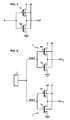
- the circuit comprises a P channel transistor T P , the source of which is connected to the first terminal for application of a power supply potential and an N channel transistor T N , the source of which is connected to the second terminal for application of a power supply potential.
- the gates of the transistors T P , T N of the circuit are connected together and connected to a common input (B in Figs. 5 and 7 , MWL# in Fig. 6 ).
- the middle point of the serial association of the transistors T P , T N forms the output of the circuit (OUT in Figs. 5 and 7 , LWL E and LWL 0 in Fig. 6 ).
- the circuit according to the first aspect of the invention is said to be a pseudo-inverter in that it has the standard structure of a CMOS inverter. However, as this will be described further subsequently, depending on the inputs which are applied on this circuit, the latter may produce other logic functions.
- the logic inversion function may moreover be achieved by setting in a standard way the first terminal for application of a power supply potential to the high state VDD and by setting the second terminal for application of a power supply potential to the low state GND.
- each of the transistors has a back control gate formed in the base substrate below the channel and capable of being biased for modulating the threshold voltage of the transistor.
- a P channel transistor is illustrated in Fig. 3a , having a back control gate BG P laid out in the base substrate under the insulating layer BOX so as to be positioned facing the front control gate G.
- the back control gate BG P is formed here by a P type doped region isolated from the base substrate by a well C N of conductivity N.
- An N channel transistor is illustrated in Fig. 3b , having a back control gate BG N laid out in the base substrate under the insulating layer so as to be positioned facing the front control gate G.
- the back control gate BG N is formed here by an N type doped region insulated from the base substrate by a well C P of conductivity P.
- the transistors are fully depleted SeOI transistors defined by a channel/body region that is thin enough to allow the field induced by the top control gate (under usual voltage conditions) to reach the buried oxide layer BOX..
- a transistor for which the channel has N type conductivity and a back control gate of conductivity P has a very high threshold voltage. This threshold voltage may then be reduced by applying a positive voltage on the back control gate.
- a transistor for which the channel has N type conductivity and a back control gate of conductivity N, as for it, has a nominal threshold voltage which may be reduced by applying a positive voltage on the back control gate.
- the type of doping of the back control gate associated with a transistor either shifts the nominal threshold voltage or not, and that the bias of the back control gate allows adjustment of the threshold voltage.
- Fig. 4 illustrates the modulation of the threshold voltage V TH of a transistor depending on the bias V BG of its back control gate. This bias is typically in the range 0V-VDD.
- An N type transistor has a nominal threshold voltage V TN0 .
- the effective threshold voltage of this transistor may be reduced from the nominal threshold voltage V TN0 by increasing the bias V BG of its back control gate, and this globally linearly according to a slope corresponding to the coefficient ⁇ related to the geometry of the transistor.
- Fig. 4 Two possible variations of the threshold voltage of an N channel transistor versus the geometry coefficient ⁇ are illustrated in Fig. 4 , in solid lines and in dotted lines, respectively. It is noticed that it proves to be possible (cf. dotted line curve) to adopt a geometry of a transistor such that the transistor is in a depletion mode (negative threshold voltage) when a sufficiently large bias is applied to its back control gate.
- a P type transistor has a nominal threshold voltage V TP0 .
- the effective threshold voltage of this transistor may be increased from the nominal threshold voltage V TP0 by reducing the bias V BG of its back control gate, and this globally linearly according to a slope corresponding to the coefficient ⁇ related to the geometry of the transistor.
- Fig. 4 Two possible variations of the threshold voltage of a P channel transistor versus the geometry coefficient ⁇ are illustrated in Fig. 4 , in solid lines and in dotted lines, respectively. It is noticed that it proves to be possible (cf. doted line curve) to adopt a geometry of a transistor such that the transistor is in a depletion mode (positive threshold voltage) when a sufficiently low bias is applied to its back control gate.
- the transistors of the circuit according to the first aspect of the invention are fully depleted.
- the benefit is thus due to the fact that such transistors have very low fluctuation of dopants (RDF: Random Dopant Fluctuation): the nominal threshold voltage is then defined very specifically, as well as the variation of the threshold voltage versus bias of the back control gate.
- At least one of the transistors of the circuit is configured so as to operate in a depletion mode under the action of a back gate signal which will sufficiently modulate its threshold voltage.
- the back control gates of the transistors T P and T N are biased by a same back gate signal (possibly with a modification of the amplitude of the back gate signal).
- transistors may be selected for which the nominal threshold voltages (V TN0 and V TP0 ) are not identical (in absolute value), so that only one of the two transistors of the circuit is capable of operating in a depletion mode.
- a back gate signal which does not have the same amplitude may also be applied to the back control gate of each of the transistors T P and T N .
- the pseudo-inverter circuit provides the logic NOR function.
- the back control gates are biased by a same back gate signal A#.
- the first terminal for application of a power supply potential is biased by the complementary signal A of the back gate signal, while the second terminal for application of a power supply potential is biased at a OFF state (low state GND).
- the transistor of the second channel type T N is configured so as to operate in a depletion mode when the back gate signal A# is at the ON state (high state H).
- ON means that the transistor is boosted and leaky. It can even be depletion if there is enough amplitude in threshold voltage modulation.
- OFF means that the threshold voltage of the transistor is elevated by the back gate control: the transistor has less leakage and less drive.
- the voltage effects by the back control gate are symmetrical for P and N channels.
- the operation of the circuit of Fig. 5 is the following, depending on the high H or low L state of inputs A and B.
- the circuit As the signal A applied to the first terminal for application of a power supply potential is high, the circuit is powered.
- the complementary signal A# applied to the back gates is such that the transistor T P remains in an enhancement mode and is therefore blocked.
- This alternative should of course be compatible with the properties that the transistor T N should have in the other cases.
- the OUT output of the circuit is then in the low state.
- the transistor T N is conducting while the transistor T P is blocked.
- the circuit As the signal A applied to the first terminal for application of a power supply potential is (sufficiently) low, the circuit is not powered.
- the transistor T P is blocked and has very low leakage current I OFF .
- the transistor T N As the back gate signal A# is in the high state, the transistor T N has a strong conduction current and therefore perfectly maintains a low state on the output OUT of the circuit.
- the transistor T N is blocked while the transistor T P is conducting.
- the circuit As the signal A applied to the first terminal for application of a power supply potential is high, the circuit is powered.
- the complementary signal A# applied to the back control gates is such that the transistor T P remains in an enhancement mode and is therefore conducting with strong conduction current. A high state is therefore perfectly maintained on the output OUT of the circuit.
- the transistor T N is blocked while the transistor T P is conducting.
- the circuit As the signal A applied to the first terminal for application of a power supply potential is (sufficiently low), the circuit is not powered.
- the transistor T P As the back gate signal A# is in the high state, the transistor T P is blocked and has very low leakage current I OFF .
- the transistor T N as for it, has very good conduction current and remains conducting insofar that the combination of the parameters t OX , t BOX and T SL is such that the transistor then operates in a depletion mode.
- the OUT output of the circuit is then in the low state.
- the signals A and B respectively act on back control and front control gates for which the oxide thicknesses separating them from the channel of the transistor are not the same (the thickness of the buried insulating BOX layer being typically larger than the dielectric gate layer separating the front control gate from the channel). Consequently, the inputs A and B are not equivalent: A is a slow input while B is a relatively fast input.
- FIG. 6 A possible application of the NOR circuit of Fig. 5 which fulfils the same logic function as the circuit of Fig. 2a , is illustrated in Fig. 6 , i.e. the embodiment of two NOR gates in parallel.
- a wordline driver circuit of a memory array comprising at least one pair of circuits 4, 5 according to Fig. 5 laid out in parallel, each circuit of the pair being intended for receiving an input signal (main wordline signal MWL#) from a row address decoder 1 and providing at the output a signal LWL E , LWL 0 intended to be used as a local wordline for a plurality of memory cells laid out as a line.
- the control of the driver circuit illustrated in Fig. 6 is the following.
- the back gate bias signal A# of the first circuit 4 of the pair of circuits is the complementary signal of the back gate signal A of the second circuit 5 of the pair of circuits.
- the first terminal for application of a power supply potential and the bias signals of back gates of each of the circuits of the pair are in the low state.
- the main wordline signal MWL# is in the high state.
- the transistors T N of the circuits 4,5 are conducting whereas the transistors T P of the circuits 4, 5 are blocked.
- the wordline driver circuit of Fig. 6 has the advantage of low power consumption. Indeed, in the standby mode, the driver circuit is not powered. Moreover, the driver circuit comprises a reduced number of components (only two transistors) so that in the active mode, switching is only observed for a reduced number of components.
- the pseudo-inverter circuit provides the logic NAND function.
- the back control gates are biased by a same back gate signal A.
- the first terminal for application of a power supply potential is biased at a high state VDD, whereas the second terminal for application of a power supply potential is biased by the complementary signal A# of the back gate signal.
- the transistor of the first channel type T P is, as for it, configured so as to operate in a depletion mode when the back gate signal A is in the low state L.
- the operation of the circuit of Fig. 5 is the following depending on the high H or low L state of the inputs A and B.
- the transistor T P is conducting and has strong conduction current because the back gate signal is in the low state.
- the transistor T N is blocked and has few leakages (a weak leakage current because of the back gate signal in the low state). In any case, it is not powered.
- the output OUT is thus in the high state.
- the transistor T N is blocked and has few leakages (a weak leakage current because of the back gate signal in the low state). In any case, it is not powered.
- the transistor T P is conducting insofar that it then operates in a depletion mode under the action of the bias signal of the back gate in the low state.
- the output OUT is thus in the high state.
- the transistor T P is conducting (but not boosted because of the high state applied to the back gate signal).
- the transistor T N is blocked (it is not in a depletion mode here)
- the output OUT is thus in the high state.
- the transistor T P is blocked (and not boosted because of the high state applied to the back gate signal).
- the transistor T N is conducting (it is not in a depletion mode here)
- the output OUT is thus in the low state.
- the transistors T N and T P may be boosted (increase in their conduction current) when this is desired because of the bias of their back control gate.
- the relatively large voltage required on the local wordline may be obtained by using transistors which globally are twice as smaller as those used in standard driver solutions.
- the size of the transistor T P is of the order of one third of that of the transistor 303 of Fig. 1
- the size of the transistor T N is of the order of one third of that of the transistor 313 of Fig. 1 (which is approximately the same as that of the transistor 303).
- the driver circuit has a size globally equal to the size (W303) of the transistor 303
- the solution proposed by the invention is thus much denser (by a factor of the order of four taking into account limitations relating to metallization) than those of standard driver solutions.
- an advantage of the invention is to make available a circuit which, depending on the inputs which are applied to it, may both provide logic INV, NOR and NAND functions, so that the whole of the standard library of CMOS cells may be described on the basis of the single circuit of the invention.
- the invention provides an original command of a (pseudo-)inverter by applying digital signals to the terminals for application of a power supply potential, rather than the classical OV and VDD power supplies.
- the digital signals may in particular be complementary to the back gate signal.
- the inputs are not equivalent, in terms of speed notably, but such a circuit may prove to be very interesting in identified contexts, such as for example for decoding circuits, or driver circuits.
Landscapes
- Engineering & Computer Science (AREA)
- Microelectronics & Electronic Packaging (AREA)
- Power Engineering (AREA)
- Physics & Mathematics (AREA)
- Ceramic Engineering (AREA)
- Condensed Matter Physics & Semiconductors (AREA)
- General Physics & Mathematics (AREA)
- Computer Hardware Design (AREA)
- Semiconductor Memories (AREA)
Applications Claiming Priority (2)
| Application Number | Priority Date | Filing Date | Title |
|---|---|---|---|
| FR1052543A FR2958441B1 (fr) | 2010-04-02 | 2010-04-02 | Circuit pseudo-inverseur sur seoi |
| US12/793,553 US8223582B2 (en) | 2010-04-02 | 2010-06-03 | Pseudo-inverter circuit on SeOI |
Publications (1)
| Publication Number | Publication Date |
|---|---|
| EP2372716A1 true EP2372716A1 (de) | 2011-10-05 |
Family
ID=44123272
Family Applications (1)
| Application Number | Title | Priority Date | Filing Date |
|---|---|---|---|
| EP10175849A Withdrawn EP2372716A1 (de) | 2010-04-02 | 2010-09-08 | Pseudo-Umkehrschaltung auf Halbleiter-auf-Isolator |
Country Status (1)
| Country | Link |
|---|---|
| EP (1) | EP2372716A1 (de) |
Cited By (1)
| Publication number | Priority date | Publication date | Assignee | Title |
|---|---|---|---|---|
| US9159400B2 (en) | 2011-03-18 | 2015-10-13 | Soitec | Semiconductor memory having staggered sense amplifiers associated with a local column decoder |
Citations (4)
| Publication number | Priority date | Publication date | Assignee | Title |
|---|---|---|---|---|
| US20060291321A1 (en) * | 2005-06-24 | 2006-12-28 | Monolithic System Technology, Inc. | Word line driver for DRAM embedded in a logic process |
| EP1744364A2 (de) * | 2005-07-11 | 2007-01-17 | Hitachi, Ltd. | Halbleiterbauelemente |
| US20090101940A1 (en) * | 2007-10-19 | 2009-04-23 | Barrows Corey K | Dual gate fet structures for flexible gate array design methodologies |
| WO2010007478A1 (en) * | 2008-06-13 | 2010-01-21 | Yale University | Improved complementary metal oxide semiconductor devices |
-
2010
- 2010-09-08 EP EP10175849A patent/EP2372716A1/de not_active Withdrawn
Patent Citations (5)
| Publication number | Priority date | Publication date | Assignee | Title |
|---|---|---|---|---|
| US20060291321A1 (en) * | 2005-06-24 | 2006-12-28 | Monolithic System Technology, Inc. | Word line driver for DRAM embedded in a logic process |
| US20070109906A1 (en) | 2005-06-24 | 2007-05-17 | Monolithic System Technology, Inc. | Word Line Driver For DRAM Embedded In A Logic Process |
| EP1744364A2 (de) * | 2005-07-11 | 2007-01-17 | Hitachi, Ltd. | Halbleiterbauelemente |
| US20090101940A1 (en) * | 2007-10-19 | 2009-04-23 | Barrows Corey K | Dual gate fet structures for flexible gate array design methodologies |
| WO2010007478A1 (en) * | 2008-06-13 | 2010-01-21 | Yale University | Improved complementary metal oxide semiconductor devices |
Non-Patent Citations (1)
| Title |
|---|
| HOON CHOI ET AL: "Improved current drivability with back-gate bias for elevated source and drain structured FD-SOI SiGe MOSFET", MICROELECTRONIC ENGINEERING, ELSEVIER PUBLISHERS BV., AMSTERDAM, NL, vol. 86, no. 11, 1 November 2009 (2009-11-01), pages 2165 - 2169, XP002579041, ISSN: 0167-9317, DOI: 10.1016/J.MEE.2009.03.015 * |
Cited By (1)
| Publication number | Priority date | Publication date | Assignee | Title |
|---|---|---|---|---|
| US9159400B2 (en) | 2011-03-18 | 2015-10-13 | Soitec | Semiconductor memory having staggered sense amplifiers associated with a local column decoder |
Similar Documents
| Publication | Publication Date | Title |
|---|---|---|
| US8654602B2 (en) | Pseudo-inverter circuit on SeOI | |
| JP3182067B2 (ja) | Dram電荷蓄積構造及びdram電荷蓄積構造用電圧昇圧回路 | |
| JP4800700B2 (ja) | 半導体装置およびそれを用いた半導体集積回路 | |
| JP4967264B2 (ja) | 半導体装置 | |
| US7042245B2 (en) | Low power consumption MIS semiconductor device | |
| US6232793B1 (en) | Switched backgate bias for FET | |
| JP2939086B2 (ja) | 半導体装置 | |
| US20020031028A1 (en) | Threshold voltage compensation circuits for low voltage and low power CMOS integrated circuits | |
| US7639066B2 (en) | Circuit and method for suppressing gate induced drain leakage | |
| US9496877B2 (en) | Pseudo-inverter circuit with multiple independent gate transistors | |
| US6839299B1 (en) | Method and structure for reducing gate leakage and threshold voltage fluctuation in memory cells | |
| JP3039245B2 (ja) | 半導体メモリ装置 | |
| EP2372716A1 (de) | Pseudo-Umkehrschaltung auf Halbleiter-auf-Isolator | |
| JP2005353274A (ja) | 半導体回路 | |
| JP2017224732A (ja) | 半導体装置 |
Legal Events
| Date | Code | Title | Description |
|---|---|---|---|
| PUAI | Public reference made under article 153(3) epc to a published international application that has entered the european phase |
Free format text: ORIGINAL CODE: 0009012 |
|
| 17P | Request for examination filed |
Effective date: 20100908 |
|
| AK | Designated contracting states |
Kind code of ref document: A1 Designated state(s): AL AT BE BG CH CY CZ DE DK EE ES FI FR GB GR HR HU IE IS IT LI LT LU LV MC MK MT NL NO PL PT RO SE SI SK SM TR |
|
| AX | Request for extension of the european patent |
Extension state: BA ME RS |
|
| RAP1 | Party data changed (applicant data changed or rights of an application transferred) |
Owner name: SOITEC |
|
| STAA | Information on the status of an ep patent application or granted ep patent |
Free format text: STATUS: THE APPLICATION HAS BEEN WITHDRAWN |
|
| 18W | Application withdrawn |
Effective date: 20140428 |