EP2369898A2 - LED-Lampe, Leuchtvorrichtung und Beleuchtungsvorrichtung - Google Patents
LED-Lampe, Leuchtvorrichtung und Beleuchtungsvorrichtung Download PDFInfo
- Publication number
- EP2369898A2 EP2369898A2 EP11158094A EP11158094A EP2369898A2 EP 2369898 A2 EP2369898 A2 EP 2369898A2 EP 11158094 A EP11158094 A EP 11158094A EP 11158094 A EP11158094 A EP 11158094A EP 2369898 A2 EP2369898 A2 EP 2369898A2
- Authority
- EP
- European Patent Office
- Prior art keywords
- led lamp
- lighting device
- discharge lamp
- lamp
- illumination device
- Prior art date
- Legal status (The legal status is an assumption and is not a legal conclusion. Google has not performed a legal analysis and makes no representation as to the accuracy of the status listed.)
- Granted
Links
- 238000005286 illumination Methods 0.000 title claims abstract description 38
- 230000015556 catabolic process Effects 0.000 abstract description 8
- 238000006731 degradation reaction Methods 0.000 abstract description 8
- 239000003990 capacitor Substances 0.000 description 30
- 238000010586 diagram Methods 0.000 description 7
- 238000007796 conventional method Methods 0.000 description 1
- 230000000694 effects Effects 0.000 description 1
- 230000003287 optical effect Effects 0.000 description 1
- 230000010355 oscillation Effects 0.000 description 1
- 238000004804 winding Methods 0.000 description 1
Images

Classifications
-
- H—ELECTRICITY
- H05—ELECTRIC TECHNIQUES NOT OTHERWISE PROVIDED FOR
- H05B—ELECTRIC HEATING; ELECTRIC LIGHT SOURCES NOT OTHERWISE PROVIDED FOR; CIRCUIT ARRANGEMENTS FOR ELECTRIC LIGHT SOURCES, IN GENERAL
- H05B45/00—Circuit arrangements for operating light-emitting diodes [LED]
- H05B45/40—Details of LED load circuits
-
- Y—GENERAL TAGGING OF NEW TECHNOLOGICAL DEVELOPMENTS; GENERAL TAGGING OF CROSS-SECTIONAL TECHNOLOGIES SPANNING OVER SEVERAL SECTIONS OF THE IPC; TECHNICAL SUBJECTS COVERED BY FORMER USPC CROSS-REFERENCE ART COLLECTIONS [XRACs] AND DIGESTS
- Y02—TECHNOLOGIES OR APPLICATIONS FOR MITIGATION OR ADAPTATION AGAINST CLIMATE CHANGE
- Y02B—CLIMATE CHANGE MITIGATION TECHNOLOGIES RELATED TO BUILDINGS, e.g. HOUSING, HOUSE APPLIANCES OR RELATED END-USER APPLICATIONS
- Y02B20/00—Energy efficient lighting technologies, e.g. halogen lamps or gas discharge lamps
- Y02B20/30—Semiconductor lamps, e.g. solid state lamps [SSL] light emitting diodes [LED] or organic LED [OLED]
Definitions
- This invention relates to an LED lamp used in combination with a discharge lamp lighting device, a lighting device used for both the LED lamp and a discharge lamp, and an illumination device equipped with the LED lamp and the lighting device.
- Patent Literature 1 JP 2009-272088A ( Fig. 1 and Claim 1)
- an LED Light Emitting Diode
- a fluorescent lamp is widely popular as a main illumination in offices, factories, ordinary houses and the like and a quantity scale of an LED illumination device is still small and the LED illumination device is in a transit period for becoming popular.
- an LED element itself is also developing and it is expected that the LED element will be reduced in cost and improved in efficiency.
- an LED lamp attachable to a fluorescent lamp illumination device has been proposed.
- Patent Literature 1 was proposed for the purpose to prevent the LED from being degraded by flowing of the over current due to the difference in voltage, current, frequency or the like depending on the individual discharge lamp lighting devices.
- the lighting device applied to the above Patent Literature1 has a series circuit including two switching elements connected between output ends of a DC current and a resonance circuit including a capacitor, a coil, a capacitor and a fluorescent lamp which is connected to both ends of one of the switching elements.
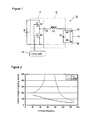
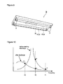
- a control part causes the switching elements to drive on/off alternately to change a driving frequency, thereby controlling precedent preheating, discharge starting and rated lighting of the fluorescent lamp. As shown in Fig.
- the voltage across the fluorescent lamp is increased to a discharge starting voltage to start the discharge after a filament of the fluorescent lamp is properly preheated by changing the driving frequency, f1 ⁇ f2 ⁇ f3, and then, the rated optical output is obtained.
- the operation point is changed in the order of a ⁇ b ⁇ c ⁇ d. In this way, the driving frequency and the operation point of the lighting device transit such as a ⁇ b ⁇ c ⁇ d.
- a load generally includes a plurality of LEDs and a rectifying circuit.
- each of the LED is basically a diode, its forward voltage VF is substantially constant and its forward current IF depends on the application condition of the power source, the impedances thereof greatly depends on an application condition. That is to say, since the impedance of the load is varied depending on an application condition of the power source from the lighting device, it is required to consider which operation point is used in combination of the lighting device and a load including the LEDs.
- the present invention has been made to solve the prescribed problems and directs to provide an LED lamp in which failures and degradation of the LEDs are suppressed even in combination with a discharge lamp lighting device and a lighting device capable of using for both of the LED lamp and a discharge lamp as well as an illumination device using thereof.
- An LED lamp according to the present invention includes a light emitting circuit having an LED adapted to emit light by an electric current inputted from a discharge lamp illumination device and a capacitive component connected in parallel to an output of the discharge lamp illumination device, wherein the LED lamp is attachable to the discharge lamp illumination device.
- a lighting device used for the discharge lamp illumination device is capable of using both of a discharge lamp and the LED lamp as a load, the lighting device has four output parts and the capacitive component between two output parts on a non-power source side, and the LED lamp is not connected to at least one output part on the non-power source side of the lighting device.
- the LED lamp according to the present invention has impedance between pins corresponding to at least one filament of the discharge lamp.
- the lighting device has impedance detecting means adapted to detect an impedance component between the pins corresponding to the filament of the discharge lamp, the impedance detecting means determines whether a mounted load is the discharge lamp or the LED lamp and a frequency sequence during starting the lighting device is changed by an output signal from the impedance detecting means.
- the illumination device according to the present invention used the LED lamp and the lighting device.
- an LED lamp a lighting device and an illumination device of the present invention
- the LED lamp in which failures and degradation of the LEDs are suppressed even in combination with a discharge lamp lighting device and the lighting device capable of using for both of the LED lamp and a discharge lamp as well as the illumination device using thereof.
- a lighting device 10 includes a direct power source E, an inverter circuit 11 having a series circuit with two N-channel type switching elements Q2 and Q3 connected between output ends of the direct power source E, a resonance circuit 12 having a capacitor C3 connected to a source of the switching element Q2 and a drain of the switching element Q3, a ballast choke coil L2 and a capacitor C4 and a control part 13 connected to gates of the switching elements Q2 and Q3.
- the lighting device 10 is changed in the driving frequency, f1 ⁇ f2 ⁇ f3 during starting to drive on/off the switching elements Q2 and Q3 alternately by the control part 13 to provide lighting control for a discharge lamp La (see Fig. 10 ).
- the output from the lighting device 10 is an AC voltage with a high frequency of approximately 50 to 150 kHz in accordance with the driving frequency.
- the lighting circuit 10 has base pins A1, A2, B1 and B2.
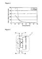
- an output voltage becomes substantially constant (the difference between two curves, i.e. a voltage difference in Fig. 2 is smaller than that in Fig.
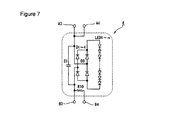
- an LED lamp 1 which is the first embodiment of the present invention has terminals A3, A4, B3 and B4 which short circuit respectively base pins A1, A2, B1 and B2 of portions corresponding to the filament of the discharge lamp La, the capacitor C1 is connected between the terminals A3, A4, B3 and B4 and a diode bridge DB including diodes D1, D2, D3 and D4 is connected in parallel to the capacitor C1. Furthermore, light emitting circuit LEDs 1 - n are connected in series with each other and are connected to the output of the diode bridge DB.
- the lighting device 10 is not operated in a phase advancing area of the resonance characteristic even if the driving frequency is changed, f1 ⁇ f2 ⁇ f3, during starting and the excessive electrical stress is not applied on the lighting device 10, the failures and degradation of the lighting device 10 can be suppressed.
- the capacitor C1 which is the capacitive component connected in parallel to the output of the discharge lamp illumination device is provided. Accordingly, in the LED lamp 1 of the first embodiment, the failures and degradation of the LED lamp 1 of the first embodiment can be suppressed in a simple configuration as well as the failures and degradation of the lighting device 10 to be combined can be suppressed.
- an LED lamp 2 of the second embodiment of the present invention has terminals A3, A4, B3 and B4 which short circuit respectively base pins A1, A2, B1 and B2 of portions corresponding to a filament of the discharge lamp La, and the capacitor C1 is connected between the terminals A3, A4, B3 and B4. Furthermore, a plurality of light emitting circuit LEDs 1 - n connected in series and a plurality of light emitting circuit LEDs m - 1 connected in series are connected in parallel in an opposing direction and are connected to the capacitor C1. In the LED lamp 2, the light emitting circuit LEDs 1 - n and the light emitting circuit LEDs m - 1 is lighted alternately depending on whether an AC voltage is positive or negative. Likewise the first embodiment, a resonance characteristic is changed by the capacitor C1.
- the possibility that an electric stress is excessively applied on both of the LED lamp 3 and the lighting device 10 can be reduced as much as possible in a simple configuration.
- the LED lamp 3 of the third embodiment of the present invention has short circuited terminals A3 and A4 of portions of a filament of a discharge lamp La on its one end and terminals B3 and B4 on the other end.
- the terminal B3 on the other side has no electric connection and the terminal A4 is connected to a capacitor C1.
- the base pin A1 is connected to the terminal A3, the base pin A2 is connected to the terminal A4, the base pin B1 is connected to the terminal B3 and the base pin B2 is connected to the terminal B4. Since the terminal B3 of the LED lamp 3 has no electric connection herein, the LED lamp 3 is not electrically connected to the capacitor C4 in the lighting device 10.
- the resonance characteristics shown in Figs. 2 and 3 are mainly determined by the impedances of the coil L2 of the resonance circuit 12 in the lighting circuit 10, the capacitor C1 which is a capacitive component added to the LED lamp 3 and the light emitting circuit LEDs 1 - n of the LED lamp 3.
- the capacitor C4 since the capacitor C4 has no influence to the resonance characteristic, the capacitor C4 can be combined to the LED lamp 3 even if the lighting device 10 has the different capacitor C4, thereby it becomes possible to suppress the failures and degradation of the LED lamp 3 and the lighting device 10 in a simple configuration.
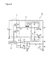
- the LED lamp 4 of the fourth embodiment of the present invention has the capacitor C1 connected between the terminal A3 and the terminal B3 and the diode bridge DB connected to the capacitor C1 in parallel.
- the light emitting circuit LEDs 1 - n are connected in series with each other and are connected to an output of the diode bridge DB.
- the terminal A3 and the terminal A4 are short circuited and a resistance R10 (for example 1 k ⁇ ) is connected to the terminal B3 and the terminal B4.
- a lighting device 20 on which the LED lamp 4 is mounted includes a direct power source E, an inverter circuit 11 having series circuit with two N-channel type switching elements Q2 and Q3 connected between output ends of the direct power source E, a resonance circuit 12 having the capacitor C3 connected to a source of the switching element Q2 and a drain of the switching element Q3, a ballast choke coil L2, a capacitor C4, a capacitor C5 and a capacitor C6, and a control part 13 connected to gates of the switching elements Q2 and Q3.
- the switching elements Q2 and Q3 is driven on/off alternately by the control part 13.
- ballast choke coil L2 Two secondary windings of the ballast choke coil L2 are connected to the output terminals A5 - A6 and B5 - B6 via the capacitor C5 and C6, respectively.
- resistors R1, R2 and R3 are connected in series between the output ends of the direct power source E, the connecting points of the resistor R1 and R2 are connected to the output terminal B6.
- a capacitor C7 is connected to the resistor R3 in parallel and the capacitor C7 is connected to each of positive terminals of comparators CP1 and CP2.
- Constant voltages V1 and V2 are inputted to negative terminals of the comparators CP1 and CP2, respectively (V1 ⁇ V2) and the outputs of the comparators CP1 and CP2 are connected to the control part 13 with pull-up resistances R4 and R5 respectively.
- the operation of the control part 13 is changed depending on the outputs of the comparators CP1 and CP2.
- the control part 13 is not oscillated.
- the oscillation is stopped as the operation of the lighting device 20.
- the control part 13 controls the frequency to change such as f1 ⁇ f2 ⁇ f3. That is to say, in the case where the load is the discharge lamp La, the control part 13 controls to change precedent preheating ⁇ discharge starting voltage ⁇ rated output.
- the output of the comparator CP1 becomes "H” and the output of the comparator CP2 becomes “L” to drive at the frequency f3 so as to be the rated output without passing through the sequence such as the precedent preheating (frequency: f1) and the discharge starting voltage (frequency: f2).
- f3 is not necessarily the rated output frequency of the discharge lamp La and may be f4 for example.
- Providing an impedance acting as the resistance R10 on the terminal B3 and the terminal B4 corresponding to the filament of the discharge lamp La in the LED lamp 4 allows to determine on a lighting device 20 side whether the load is the discharge lamp La or the LED lamp 4 in a simple configuration in addition to detecting a no load condition. Furthermore, determining whether the load mounted in this manner is the discharge lamp La or the LED lamp 4 and changing a frequency sequence of the lighting device 20 during stating by an output signal from impedance detecting means causes the rated lighting through an appropriate sequence in the case where the load is the discharge lamp La and causes the rated lighting without passing through the unrequited sequence in the case where the load is the LED lamp 4. That is to say, changing the frequency sequence during starting depending on the loads allows each load to be controlled suitably.
- the illumination device 30 can use both of the discharge lamp La and the LED lamp 4 as the load for two pairs of sockets 31. Therefore, user-availability can be improved. As described above for example, while it is expected that the LED will be improved in cost and performance in future, it is possible to switch from the discharge lamp La to the LED lamp 4 when a user agrees with the cost and performance thereof. In addition, in the case where a number of illumination devices are disposed such as in office, when the discharge lamp La and the LED lamp 4 are used separately, the discharge lamp La and the LED lamp 4 which act as the light source can be changed together by changing the layout or the like.
- providing the impedance acting as the resistance R10 on the terminal B3 and the terminal B4 corresponding to the filament of the discharge lamp La allows to determine on the lighting device 20 side whether the load is the discharge lamp La or the LED lamp 4, or otherwise no load is mounted, thereby the handling ability can be improved.
- the impedance detecting means adapted to detect the impedance component acting as the resistance R10 between the terminals B3 and B4 corresponding to the filament of the discharge lamp La to determine whether the mounted load is the discharge lamp La or the LED lamp 4 and changing the frequency sequence of the lighting device 20 during starting by the output signal from the impedance detecting means allow each load to be controlled suitably.
- the illumination device 30 equipped with the LED lamp 4 and the lighting device 20 the illumination device 30 capable of using both of the discharge lamp La and the LED lamp 4 as the loads can be provided.
- the user may switch from the discharge lamp La to the LED lamp 4 when a user agrees with the cost and performance and a user need not to buy new one in vain. Therefore, the illumination fixture 30 which is useful for the user can be provided.
Landscapes
- Circuit Arrangement For Electric Light Sources In General (AREA)
- Arrangement Of Elements, Cooling, Sealing, Or The Like Of Lighting Devices (AREA)
- Non-Portable Lighting Devices Or Systems Thereof (AREA)
Applications Claiming Priority (1)
| Application Number | Priority Date | Filing Date | Title |
|---|---|---|---|
| JP2010066467A JP2011198696A (ja) | 2010-03-23 | 2010-03-23 | Ledランプ、点灯装置および照明装置 |
Publications (3)
| Publication Number | Publication Date |
|---|---|
| EP2369898A2 true EP2369898A2 (de) | 2011-09-28 |
| EP2369898A3 EP2369898A3 (de) | 2016-09-07 |
| EP2369898B1 EP2369898B1 (de) | 2019-01-02 |
Family
ID=44260378
Family Applications (1)
| Application Number | Title | Priority Date | Filing Date |
|---|---|---|---|
| EP11158094.0A Not-in-force EP2369898B1 (de) | 2010-03-23 | 2011-03-14 | LED-Lampe, Leuchtvorrichtung und Beleuchtungsvorrichtung |
Country Status (2)
| Country | Link |
|---|---|
| EP (1) | EP2369898B1 (de) |
| JP (1) | JP2011198696A (de) |
Families Citing this family (1)
| Publication number | Priority date | Publication date | Assignee | Title |
|---|---|---|---|---|
| JP6002717B2 (ja) * | 2014-06-23 | 2016-10-05 | Jcテクノロジー株式会社 | Ledランプ |
Citations (1)
| Publication number | Priority date | Publication date | Assignee | Title |
|---|---|---|---|---|
| JP2009272088A (ja) | 2008-05-02 | 2009-11-19 | Rohm Co Ltd | 一般用蛍光灯照明器具に取り付け可能なledランプ |
Family Cites Families (3)
| Publication number | Priority date | Publication date | Assignee | Title |
|---|---|---|---|---|
| JPH11307290A (ja) * | 1998-04-23 | 1999-11-05 | Matsushita Electric Works Ltd | 放電灯点灯装置 |
| KR100891740B1 (ko) * | 2007-11-13 | 2009-04-03 | 김철 | 형광등기구의 엘이디램프 연결장치 |
| CN102017796B (zh) * | 2008-05-05 | 2013-06-19 | 皇家飞利浦电子股份有限公司 | 发光二极管系统 |
-
2010
- 2010-03-23 JP JP2010066467A patent/JP2011198696A/ja active Pending
-
2011
- 2011-03-14 EP EP11158094.0A patent/EP2369898B1/de not_active Not-in-force
Patent Citations (1)
| Publication number | Priority date | Publication date | Assignee | Title |
|---|---|---|---|---|
| JP2009272088A (ja) | 2008-05-02 | 2009-11-19 | Rohm Co Ltd | 一般用蛍光灯照明器具に取り付け可能なledランプ |
Also Published As
| Publication number | Publication date |
|---|---|
| EP2369898A3 (de) | 2016-09-07 |
| EP2369898B1 (de) | 2019-01-02 |
| JP2011198696A (ja) | 2011-10-06 |
Similar Documents
| Publication | Publication Date | Title |
|---|---|---|
| EP2914065B1 (de) | Beleuchtungslampe und beleuchtungsvorrichtung | |
| JP5076106B2 (ja) | 高効率ac led駆動回路 | |
| US8581512B2 (en) | Light source module, lighting apparatus, and illumination device using the same | |
| JP4994101B2 (ja) | Led照明灯及び該led照明灯を用いた灯器具 | |
| CN102164440B (zh) | 点灯装置及使用该点灯装置的照明器具 | |
| EP2424332A1 (de) | Gleichstromquelleneinheit und LED-Lampensystem | |
| RU2587475C2 (ru) | Устройство драйвера и способ возбуждения для возбуждения нагрузки, в частности сборки светодиодов | |
| EP2326148A2 (de) | Ansteuerungsvorrichtung für eine Beleuchtungsschaltung und Beleuchtungsvorrichtung | |
| US20140159592A1 (en) | Led light tube compatible with light fixture having electronic ballast or magnetic ballast | |
| US7420332B2 (en) | LED lighting device | |
| JP6502375B2 (ja) | 蛍光灯互換タイプのled照明装置とそのための感電保護装置 | |
| EP2369898B1 (de) | LED-Lampe, Leuchtvorrichtung und Beleuchtungsvorrichtung | |
| CN100386001C (zh) | 给光源供电的装置和方法 | |
| JP2011090970A (ja) | Led非常用照明装置 | |
| JP6011676B1 (ja) | 照明灯、照明装置、及び点灯制御回路 | |
| JP5385815B2 (ja) | 点灯装置及びそれを用いた照明器具 | |
| KR101446836B1 (ko) | 상태 모니터링 기능을 구비한 형광등 호환형 엘이디 램프 | |
| EP2034587A2 (de) | Verfahren und Anordnung in Verbindung mit einer Notbeleuchtung | |
| JP2017517854A (ja) | 無線制御による照明回路の駆動 | |
| JP5457875B2 (ja) | 点灯装置及びそれを用いた照明器具 | |
| US11647573B2 (en) | Driver circuit with reduced current ripple | |
| US20090001899A1 (en) | Fluorescent Lamp With Built-In Anion Generator | |
| KR101558980B1 (ko) | 개선된 led 형광램프 및 이를 채용하는 등기구 | |
| JP6331593B2 (ja) | 照明灯及び照明装置 | |
| JP2008293836A (ja) | 放電灯点灯装置及びこれを用いた照明器具 |
Legal Events
| Date | Code | Title | Description |
|---|---|---|---|
| PUAI | Public reference made under article 153(3) epc to a published international application that has entered the european phase |
Free format text: ORIGINAL CODE: 0009012 |
|
| AK | Designated contracting states |
Kind code of ref document: A2 Designated state(s): AL AT BE BG CH CY CZ DE DK EE ES FI FR GB GR HR HU IE IS IT LI LT LU LV MC MK MT NL NO PL PT RO RS SE SI SK SM TR |
|
| AX | Request for extension of the european patent |
Extension state: BA ME |
|
| RAP1 | Party data changed (applicant data changed or rights of an application transferred) |
Owner name: PANASONIC CORPORATION |
|
| RAP1 | Party data changed (applicant data changed or rights of an application transferred) |
Owner name: PANASONIC INTELLECTUAL PROPERTY MANAGEMENT CO., LT |
|
| PUAL | Search report despatched |
Free format text: ORIGINAL CODE: 0009013 |
|
| AK | Designated contracting states |
Kind code of ref document: A3 Designated state(s): AL AT BE BG CH CY CZ DE DK EE ES FI FR GB GR HR HU IE IS IT LI LT LU LV MC MK MT NL NO PL PT RO RS SE SI SK SM TR |
|
| AX | Request for extension of the european patent |
Extension state: BA ME |
|
| RIC1 | Information provided on ipc code assigned before grant |
Ipc: H05B 33/08 20060101AFI20160801BHEP |
|
| 17P | Request for examination filed |
Effective date: 20161020 |
|
| RBV | Designated contracting states (corrected) |
Designated state(s): AL AT BE BG CH CY CZ DE DK EE ES FI FR GB GR HR HU IE IS IT LI LT LU LV MC MK MT NL NO PL PT RO RS SE SI SK SM TR |
|
| GRAP | Despatch of communication of intention to grant a patent |
Free format text: ORIGINAL CODE: EPIDOSNIGR1 |
|
| STAA | Information on the status of an ep patent application or granted ep patent |
Free format text: STATUS: GRANT OF PATENT IS INTENDED |
|
| INTG | Intention to grant announced |
Effective date: 20180925 |
|
| GRAS | Grant fee paid |
Free format text: ORIGINAL CODE: EPIDOSNIGR3 |
|
| GRAA | (expected) grant |
Free format text: ORIGINAL CODE: 0009210 |
|
| STAA | Information on the status of an ep patent application or granted ep patent |
Free format text: STATUS: THE PATENT HAS BEEN GRANTED |
|
| AK | Designated contracting states |
Kind code of ref document: B1 Designated state(s): AL AT BE BG CH CY CZ DE DK EE ES FI FR GB GR HR HU IE IS IT LI LT LU LV MC MK MT NL NO PL PT RO RS SE SI SK SM TR |
|
| REG | Reference to a national code |
Ref country code: GB Ref legal event code: FG4D |
|
| REG | Reference to a national code |
Ref country code: CH Ref legal event code: EP Ref country code: AT Ref legal event code: REF Ref document number: 1086132 Country of ref document: AT Kind code of ref document: T Effective date: 20190115 |
|
| REG | Reference to a national code |
Ref country code: IE Ref legal event code: FG4D |
|
| REG | Reference to a national code |
Ref country code: DE Ref legal event code: R096 Ref document number: 602011055293 Country of ref document: DE |
|
| REG | Reference to a national code |
Ref country code: NL Ref legal event code: MP Effective date: 20190102 |
|
| REG | Reference to a national code |
Ref country code: LT Ref legal event code: MG4D |
|
| REG | Reference to a national code |
Ref country code: AT Ref legal event code: MK05 Ref document number: 1086132 Country of ref document: AT Kind code of ref document: T Effective date: 20190102 |
|
| PG25 | Lapsed in a contracting state [announced via postgrant information from national office to epo] |
Ref country code: NL Free format text: LAPSE BECAUSE OF FAILURE TO SUBMIT A TRANSLATION OF THE DESCRIPTION OR TO PAY THE FEE WITHIN THE PRESCRIBED TIME-LIMIT Effective date: 20190102 |
|
| PG25 | Lapsed in a contracting state [announced via postgrant information from national office to epo] |
Ref country code: PT Free format text: LAPSE BECAUSE OF FAILURE TO SUBMIT A TRANSLATION OF THE DESCRIPTION OR TO PAY THE FEE WITHIN THE PRESCRIBED TIME-LIMIT Effective date: 20190502 Ref country code: ES Free format text: LAPSE BECAUSE OF FAILURE TO SUBMIT A TRANSLATION OF THE DESCRIPTION OR TO PAY THE FEE WITHIN THE PRESCRIBED TIME-LIMIT Effective date: 20190102 Ref country code: LT Free format text: LAPSE BECAUSE OF FAILURE TO SUBMIT A TRANSLATION OF THE DESCRIPTION OR TO PAY THE FEE WITHIN THE PRESCRIBED TIME-LIMIT Effective date: 20190102 Ref country code: NO Free format text: LAPSE BECAUSE OF FAILURE TO SUBMIT A TRANSLATION OF THE DESCRIPTION OR TO PAY THE FEE WITHIN THE PRESCRIBED TIME-LIMIT Effective date: 20190402 Ref country code: FI Free format text: LAPSE BECAUSE OF FAILURE TO SUBMIT A TRANSLATION OF THE DESCRIPTION OR TO PAY THE FEE WITHIN THE PRESCRIBED TIME-LIMIT Effective date: 20190102 Ref country code: PL Free format text: LAPSE BECAUSE OF FAILURE TO SUBMIT A TRANSLATION OF THE DESCRIPTION OR TO PAY THE FEE WITHIN THE PRESCRIBED TIME-LIMIT Effective date: 20190102 Ref country code: SE Free format text: LAPSE BECAUSE OF FAILURE TO SUBMIT A TRANSLATION OF THE DESCRIPTION OR TO PAY THE FEE WITHIN THE PRESCRIBED TIME-LIMIT Effective date: 20190102 |
|
| PGFP | Annual fee paid to national office [announced via postgrant information from national office to epo] |
Ref country code: DE Payment date: 20190430 Year of fee payment: 9 |
|
| PG25 | Lapsed in a contracting state [announced via postgrant information from national office to epo] |
Ref country code: BG Free format text: LAPSE BECAUSE OF FAILURE TO SUBMIT A TRANSLATION OF THE DESCRIPTION OR TO PAY THE FEE WITHIN THE PRESCRIBED TIME-LIMIT Effective date: 20190402 Ref country code: GR Free format text: LAPSE BECAUSE OF FAILURE TO SUBMIT A TRANSLATION OF THE DESCRIPTION OR TO PAY THE FEE WITHIN THE PRESCRIBED TIME-LIMIT Effective date: 20190403 Ref country code: HR Free format text: LAPSE BECAUSE OF FAILURE TO SUBMIT A TRANSLATION OF THE DESCRIPTION OR TO PAY THE FEE WITHIN THE PRESCRIBED TIME-LIMIT Effective date: 20190102 Ref country code: RS Free format text: LAPSE BECAUSE OF FAILURE TO SUBMIT A TRANSLATION OF THE DESCRIPTION OR TO PAY THE FEE WITHIN THE PRESCRIBED TIME-LIMIT Effective date: 20190102 Ref country code: IS Free format text: LAPSE BECAUSE OF FAILURE TO SUBMIT A TRANSLATION OF THE DESCRIPTION OR TO PAY THE FEE WITHIN THE PRESCRIBED TIME-LIMIT Effective date: 20190502 Ref country code: LV Free format text: LAPSE BECAUSE OF FAILURE TO SUBMIT A TRANSLATION OF THE DESCRIPTION OR TO PAY THE FEE WITHIN THE PRESCRIBED TIME-LIMIT Effective date: 20190102 |
|
| REG | Reference to a national code |
Ref country code: DE Ref legal event code: R097 Ref document number: 602011055293 Country of ref document: DE |
|
| PG25 | Lapsed in a contracting state [announced via postgrant information from national office to epo] |
Ref country code: RO Free format text: LAPSE BECAUSE OF FAILURE TO SUBMIT A TRANSLATION OF THE DESCRIPTION OR TO PAY THE FEE WITHIN THE PRESCRIBED TIME-LIMIT Effective date: 20190102 Ref country code: IT Free format text: LAPSE BECAUSE OF FAILURE TO SUBMIT A TRANSLATION OF THE DESCRIPTION OR TO PAY THE FEE WITHIN THE PRESCRIBED TIME-LIMIT Effective date: 20190102 Ref country code: SK Free format text: LAPSE BECAUSE OF FAILURE TO SUBMIT A TRANSLATION OF THE DESCRIPTION OR TO PAY THE FEE WITHIN THE PRESCRIBED TIME-LIMIT Effective date: 20190102 Ref country code: CZ Free format text: LAPSE BECAUSE OF FAILURE TO SUBMIT A TRANSLATION OF THE DESCRIPTION OR TO PAY THE FEE WITHIN THE PRESCRIBED TIME-LIMIT Effective date: 20190102 Ref country code: AT Free format text: LAPSE BECAUSE OF FAILURE TO SUBMIT A TRANSLATION OF THE DESCRIPTION OR TO PAY THE FEE WITHIN THE PRESCRIBED TIME-LIMIT Effective date: 20190102 Ref country code: DK Free format text: LAPSE BECAUSE OF FAILURE TO SUBMIT A TRANSLATION OF THE DESCRIPTION OR TO PAY THE FEE WITHIN THE PRESCRIBED TIME-LIMIT Effective date: 20190102 Ref country code: MC Free format text: LAPSE BECAUSE OF FAILURE TO SUBMIT A TRANSLATION OF THE DESCRIPTION OR TO PAY THE FEE WITHIN THE PRESCRIBED TIME-LIMIT Effective date: 20190102 Ref country code: AL Free format text: LAPSE BECAUSE OF FAILURE TO SUBMIT A TRANSLATION OF THE DESCRIPTION OR TO PAY THE FEE WITHIN THE PRESCRIBED TIME-LIMIT Effective date: 20190102 Ref country code: EE Free format text: LAPSE BECAUSE OF FAILURE TO SUBMIT A TRANSLATION OF THE DESCRIPTION OR TO PAY THE FEE WITHIN THE PRESCRIBED TIME-LIMIT Effective date: 20190102 |
|
| REG | Reference to a national code |
Ref country code: CH Ref legal event code: PL |
|
| PLBE | No opposition filed within time limit |
Free format text: ORIGINAL CODE: 0009261 |
|
| STAA | Information on the status of an ep patent application or granted ep patent |
Free format text: STATUS: NO OPPOSITION FILED WITHIN TIME LIMIT |
|
| REG | Reference to a national code |
Ref country code: DE Ref legal event code: R079 Ref document number: 602011055293 Country of ref document: DE Free format text: PREVIOUS MAIN CLASS: H05B0033080000 Ipc: H05B0045000000 |
|
| PG25 | Lapsed in a contracting state [announced via postgrant information from national office to epo] |
Ref country code: LU Free format text: LAPSE BECAUSE OF NON-PAYMENT OF DUE FEES Effective date: 20190314 Ref country code: SM Free format text: LAPSE BECAUSE OF FAILURE TO SUBMIT A TRANSLATION OF THE DESCRIPTION OR TO PAY THE FEE WITHIN THE PRESCRIBED TIME-LIMIT Effective date: 20190102 |
|
| REG | Reference to a national code |
Ref country code: BE Ref legal event code: MM Effective date: 20190331 |
|
| 26N | No opposition filed |
Effective date: 20191003 |
|
| GBPC | Gb: european patent ceased through non-payment of renewal fee |
Effective date: 20190402 |
|
| PG25 | Lapsed in a contracting state [announced via postgrant information from national office to epo] |
Ref country code: LI Free format text: LAPSE BECAUSE OF NON-PAYMENT OF DUE FEES Effective date: 20190331 Ref country code: GB Free format text: LAPSE BECAUSE OF NON-PAYMENT OF DUE FEES Effective date: 20190402 Ref country code: CH Free format text: LAPSE BECAUSE OF NON-PAYMENT OF DUE FEES Effective date: 20190331 Ref country code: IE Free format text: LAPSE BECAUSE OF NON-PAYMENT OF DUE FEES Effective date: 20190314 |
|
| PG25 | Lapsed in a contracting state [announced via postgrant information from national office to epo] |
Ref country code: SI Free format text: LAPSE BECAUSE OF FAILURE TO SUBMIT A TRANSLATION OF THE DESCRIPTION OR TO PAY THE FEE WITHIN THE PRESCRIBED TIME-LIMIT Effective date: 20190102 Ref country code: FR Free format text: LAPSE BECAUSE OF NON-PAYMENT OF DUE FEES Effective date: 20190331 Ref country code: BE Free format text: LAPSE BECAUSE OF NON-PAYMENT OF DUE FEES Effective date: 20190331 |
|
| PG25 | Lapsed in a contracting state [announced via postgrant information from national office to epo] |
Ref country code: TR Free format text: LAPSE BECAUSE OF FAILURE TO SUBMIT A TRANSLATION OF THE DESCRIPTION OR TO PAY THE FEE WITHIN THE PRESCRIBED TIME-LIMIT Effective date: 20190102 |
|
| PG25 | Lapsed in a contracting state [announced via postgrant information from national office to epo] |
Ref country code: MT Free format text: LAPSE BECAUSE OF NON-PAYMENT OF DUE FEES Effective date: 20190314 |
|
| REG | Reference to a national code |
Ref country code: DE Ref legal event code: R119 Ref document number: 602011055293 Country of ref document: DE |
|
| PG25 | Lapsed in a contracting state [announced via postgrant information from national office to epo] |
Ref country code: DE Free format text: LAPSE BECAUSE OF NON-PAYMENT OF DUE FEES Effective date: 20201001 |
|
| PG25 | Lapsed in a contracting state [announced via postgrant information from national office to epo] |
Ref country code: CY Free format text: LAPSE BECAUSE OF FAILURE TO SUBMIT A TRANSLATION OF THE DESCRIPTION OR TO PAY THE FEE WITHIN THE PRESCRIBED TIME-LIMIT Effective date: 20190102 |
|
| PG25 | Lapsed in a contracting state [announced via postgrant information from national office to epo] |
Ref country code: HU Free format text: LAPSE BECAUSE OF FAILURE TO SUBMIT A TRANSLATION OF THE DESCRIPTION OR TO PAY THE FEE WITHIN THE PRESCRIBED TIME-LIMIT; INVALID AB INITIO Effective date: 20110314 |
|
| PG25 | Lapsed in a contracting state [announced via postgrant information from national office to epo] |
Ref country code: MK Free format text: LAPSE BECAUSE OF FAILURE TO SUBMIT A TRANSLATION OF THE DESCRIPTION OR TO PAY THE FEE WITHIN THE PRESCRIBED TIME-LIMIT Effective date: 20190102 |