EP2369617A2 - Semiconductor device and method of manufacturing the same - Google Patents
Semiconductor device and method of manufacturing the same Download PDFInfo
- Publication number
- EP2369617A2 EP2369617A2 EP11155929A EP11155929A EP2369617A2 EP 2369617 A2 EP2369617 A2 EP 2369617A2 EP 11155929 A EP11155929 A EP 11155929A EP 11155929 A EP11155929 A EP 11155929A EP 2369617 A2 EP2369617 A2 EP 2369617A2
- Authority
- EP
- European Patent Office
- Prior art keywords
- bump
- bumps
- semiconductor element
- distance
- semiconductor device
- Prior art date
- Legal status (The legal status is an assumption and is not a legal conclusion. Google has not performed a legal analysis and makes no representation as to the accuracy of the status listed.)
- Withdrawn
Links
Images






Classifications
-
- H—ELECTRICITY
- H10—SEMICONDUCTOR DEVICES; ELECTRIC SOLID-STATE DEVICES NOT OTHERWISE PROVIDED FOR
- H10W—GENERIC PACKAGES, INTERCONNECTIONS, CONNECTORS OR OTHER CONSTRUCTIONAL DETAILS OF DEVICES COVERED BY CLASS H10
- H10W74/00—Encapsulations, e.g. protective coatings
- H10W74/10—Encapsulations, e.g. protective coatings characterised by their shape or disposition
- H10W74/131—Encapsulations, e.g. protective coatings characterised by their shape or disposition the semiconductor body being only partially enclosed
- H10W74/147—Encapsulations, e.g. protective coatings characterised by their shape or disposition the semiconductor body being only partially enclosed the encapsulations being multilayered
-
- H—ELECTRICITY
- H10—SEMICONDUCTOR DEVICES; ELECTRIC SOLID-STATE DEVICES NOT OTHERWISE PROVIDED FOR
- H10W—GENERIC PACKAGES, INTERCONNECTIONS, CONNECTORS OR OTHER CONSTRUCTIONAL DETAILS OF DEVICES COVERED BY CLASS H10
- H10W90/00—Package configurations
- H10W90/701—Package configurations characterised by the relative positions of pads or connectors relative to package parts
-
- H—ELECTRICITY
- H10—SEMICONDUCTOR DEVICES; ELECTRIC SOLID-STATE DEVICES NOT OTHERWISE PROVIDED FOR
- H10W—GENERIC PACKAGES, INTERCONNECTIONS, CONNECTORS OR OTHER CONSTRUCTIONAL DETAILS OF DEVICES COVERED BY CLASS H10
- H10W70/00—Package substrates; Interposers; Redistribution layers [RDL]
- H10W70/01—Manufacture or treatment
- H10W70/05—Manufacture or treatment of insulating or insulated package substrates, or of interposers, or of redistribution layers
-
- H—ELECTRICITY
- H10—SEMICONDUCTOR DEVICES; ELECTRIC SOLID-STATE DEVICES NOT OTHERWISE PROVIDED FOR
- H10W—GENERIC PACKAGES, INTERCONNECTIONS, CONNECTORS OR OTHER CONSTRUCTIONAL DETAILS OF DEVICES COVERED BY CLASS H10
- H10W70/00—Package substrates; Interposers; Redistribution layers [RDL]
- H10W70/60—Insulating or insulated package substrates; Interposers; Redistribution layers
-
- H—ELECTRICITY
- H10—SEMICONDUCTOR DEVICES; ELECTRIC SOLID-STATE DEVICES NOT OTHERWISE PROVIDED FOR
- H10W—GENERIC PACKAGES, INTERCONNECTIONS, CONNECTORS OR OTHER CONSTRUCTIONAL DETAILS OF DEVICES COVERED BY CLASS H10
- H10W70/00—Package substrates; Interposers; Redistribution layers [RDL]
- H10W70/60—Insulating or insulated package substrates; Interposers; Redistribution layers
- H10W70/62—Insulating or insulated package substrates; Interposers; Redistribution layers characterised by their interconnections
- H10W70/66—Conductive materials thereof
-
- H—ELECTRICITY
- H10—SEMICONDUCTOR DEVICES; ELECTRIC SOLID-STATE DEVICES NOT OTHERWISE PROVIDED FOR
- H10W—GENERIC PACKAGES, INTERCONNECTIONS, CONNECTORS OR OTHER CONSTRUCTIONAL DETAILS OF DEVICES COVERED BY CLASS H10
- H10W72/00—Interconnections or connectors in packages
- H10W72/01—Manufacture or treatment
- H10W72/012—Manufacture or treatment of bump connectors, dummy bumps or thermal bumps
- H10W72/01221—Manufacture or treatment of bump connectors, dummy bumps or thermal bumps using local deposition
- H10W72/01225—Manufacture or treatment of bump connectors, dummy bumps or thermal bumps using local deposition in solid form, e.g. by using a powder or by stud bumping
-
- H—ELECTRICITY
- H10—SEMICONDUCTOR DEVICES; ELECTRIC SOLID-STATE DEVICES NOT OTHERWISE PROVIDED FOR
- H10W—GENERIC PACKAGES, INTERCONNECTIONS, CONNECTORS OR OTHER CONSTRUCTIONAL DETAILS OF DEVICES COVERED BY CLASS H10
- H10W72/00—Interconnections or connectors in packages
- H10W72/01—Manufacture or treatment
- H10W72/012—Manufacture or treatment of bump connectors, dummy bumps or thermal bumps
- H10W72/01231—Manufacture or treatment of bump connectors, dummy bumps or thermal bumps using blanket deposition
- H10W72/01233—Manufacture or treatment of bump connectors, dummy bumps or thermal bumps using blanket deposition in liquid form, e.g. spin coating, spray coating or immersion coating
- H10W72/01235—Manufacture or treatment of bump connectors, dummy bumps or thermal bumps using blanket deposition in liquid form, e.g. spin coating, spray coating or immersion coating by plating, e.g. electroless plating or electroplating
-
- H—ELECTRICITY
- H10—SEMICONDUCTOR DEVICES; ELECTRIC SOLID-STATE DEVICES NOT OTHERWISE PROVIDED FOR
- H10W—GENERIC PACKAGES, INTERCONNECTIONS, CONNECTORS OR OTHER CONSTRUCTIONAL DETAILS OF DEVICES COVERED BY CLASS H10
- H10W72/00—Interconnections or connectors in packages
- H10W72/01—Manufacture or treatment
- H10W72/012—Manufacture or treatment of bump connectors, dummy bumps or thermal bumps
- H10W72/01251—Changing the shapes of bumps
- H10W72/01255—Changing the shapes of bumps by using masks
-
- H—ELECTRICITY
- H10—SEMICONDUCTOR DEVICES; ELECTRIC SOLID-STATE DEVICES NOT OTHERWISE PROVIDED FOR
- H10W—GENERIC PACKAGES, INTERCONNECTIONS, CONNECTORS OR OTHER CONSTRUCTIONAL DETAILS OF DEVICES COVERED BY CLASS H10
- H10W72/00—Interconnections or connectors in packages
- H10W72/01—Manufacture or treatment
- H10W72/019—Manufacture or treatment of bond pads
-
- H—ELECTRICITY
- H10—SEMICONDUCTOR DEVICES; ELECTRIC SOLID-STATE DEVICES NOT OTHERWISE PROVIDED FOR
- H10W—GENERIC PACKAGES, INTERCONNECTIONS, CONNECTORS OR OTHER CONSTRUCTIONAL DETAILS OF DEVICES COVERED BY CLASS H10
- H10W72/00—Interconnections or connectors in packages
- H10W72/01—Manufacture or treatment
- H10W72/019—Manufacture or treatment of bond pads
- H10W72/01931—Manufacture or treatment of bond pads using blanket deposition
- H10W72/01938—Manufacture or treatment of bond pads using blanket deposition in gaseous form, e.g. by CVD or PVD
-
- H—ELECTRICITY
- H10—SEMICONDUCTOR DEVICES; ELECTRIC SOLID-STATE DEVICES NOT OTHERWISE PROVIDED FOR
- H10W—GENERIC PACKAGES, INTERCONNECTIONS, CONNECTORS OR OTHER CONSTRUCTIONAL DETAILS OF DEVICES COVERED BY CLASS H10
- H10W72/00—Interconnections or connectors in packages
- H10W72/01—Manufacture or treatment
- H10W72/0198—Manufacture or treatment batch processes
-
- H—ELECTRICITY
- H10—SEMICONDUCTOR DEVICES; ELECTRIC SOLID-STATE DEVICES NOT OTHERWISE PROVIDED FOR
- H10W—GENERIC PACKAGES, INTERCONNECTIONS, CONNECTORS OR OTHER CONSTRUCTIONAL DETAILS OF DEVICES COVERED BY CLASS H10
- H10W72/00—Interconnections or connectors in packages
- H10W72/071—Connecting or disconnecting
- H10W72/072—Connecting or disconnecting of bump connectors
-
- H—ELECTRICITY
- H10—SEMICONDUCTOR DEVICES; ELECTRIC SOLID-STATE DEVICES NOT OTHERWISE PROVIDED FOR
- H10W—GENERIC PACKAGES, INTERCONNECTIONS, CONNECTORS OR OTHER CONSTRUCTIONAL DETAILS OF DEVICES COVERED BY CLASS H10
- H10W72/00—Interconnections or connectors in packages
- H10W72/071—Connecting or disconnecting
- H10W72/072—Connecting or disconnecting of bump connectors
- H10W72/07231—Techniques
- H10W72/07232—Compression bonding, e.g. thermocompression bonding
-
- H—ELECTRICITY
- H10—SEMICONDUCTOR DEVICES; ELECTRIC SOLID-STATE DEVICES NOT OTHERWISE PROVIDED FOR
- H10W—GENERIC PACKAGES, INTERCONNECTIONS, CONNECTORS OR OTHER CONSTRUCTIONAL DETAILS OF DEVICES COVERED BY CLASS H10
- H10W72/00—Interconnections or connectors in packages
- H10W72/071—Connecting or disconnecting
- H10W72/072—Connecting or disconnecting of bump connectors
- H10W72/07231—Techniques
- H10W72/07232—Compression bonding, e.g. thermocompression bonding
- H10W72/07233—Ultrasonic bonding, e.g. thermosonic bonding
-
- H—ELECTRICITY
- H10—SEMICONDUCTOR DEVICES; ELECTRIC SOLID-STATE DEVICES NOT OTHERWISE PROVIDED FOR
- H10W—GENERIC PACKAGES, INTERCONNECTIONS, CONNECTORS OR OTHER CONSTRUCTIONAL DETAILS OF DEVICES COVERED BY CLASS H10
- H10W72/00—Interconnections or connectors in packages
- H10W72/071—Connecting or disconnecting
- H10W72/072—Connecting or disconnecting of bump connectors
- H10W72/07231—Techniques
- H10W72/07236—Soldering or alloying
-
- H—ELECTRICITY
- H10—SEMICONDUCTOR DEVICES; ELECTRIC SOLID-STATE DEVICES NOT OTHERWISE PROVIDED FOR
- H10W—GENERIC PACKAGES, INTERCONNECTIONS, CONNECTORS OR OTHER CONSTRUCTIONAL DETAILS OF DEVICES COVERED BY CLASS H10
- H10W72/00—Interconnections or connectors in packages
- H10W72/071—Connecting or disconnecting
- H10W72/073—Connecting or disconnecting of die-attach connectors
-
- H—ELECTRICITY
- H10—SEMICONDUCTOR DEVICES; ELECTRIC SOLID-STATE DEVICES NOT OTHERWISE PROVIDED FOR
- H10W—GENERIC PACKAGES, INTERCONNECTIONS, CONNECTORS OR OTHER CONSTRUCTIONAL DETAILS OF DEVICES COVERED BY CLASS H10
- H10W72/00—Interconnections or connectors in packages
- H10W72/20—Bump connectors, e.g. solder bumps or copper pillars; Dummy bumps; Thermal bumps
- H10W72/221—Structures or relative sizes
- H10W72/227—Multiple bumps having different sizes
-
- H—ELECTRICITY
- H10—SEMICONDUCTOR DEVICES; ELECTRIC SOLID-STATE DEVICES NOT OTHERWISE PROVIDED FOR
- H10W—GENERIC PACKAGES, INTERCONNECTIONS, CONNECTORS OR OTHER CONSTRUCTIONAL DETAILS OF DEVICES COVERED BY CLASS H10
- H10W72/00—Interconnections or connectors in packages
- H10W72/20—Bump connectors, e.g. solder bumps or copper pillars; Dummy bumps; Thermal bumps
- H10W72/231—Shapes
- H10W72/232—Plan-view shape, i.e. in top view
-
- H—ELECTRICITY
- H10—SEMICONDUCTOR DEVICES; ELECTRIC SOLID-STATE DEVICES NOT OTHERWISE PROVIDED FOR
- H10W—GENERIC PACKAGES, INTERCONNECTIONS, CONNECTORS OR OTHER CONSTRUCTIONAL DETAILS OF DEVICES COVERED BY CLASS H10
- H10W72/00—Interconnections or connectors in packages
- H10W72/20—Bump connectors, e.g. solder bumps or copper pillars; Dummy bumps; Thermal bumps
- H10W72/241—Dispositions, e.g. layouts
- H10W72/242—Dispositions, e.g. layouts relative to the surface, e.g. recessed, protruding
-
- H—ELECTRICITY
- H10—SEMICONDUCTOR DEVICES; ELECTRIC SOLID-STATE DEVICES NOT OTHERWISE PROVIDED FOR
- H10W—GENERIC PACKAGES, INTERCONNECTIONS, CONNECTORS OR OTHER CONSTRUCTIONAL DETAILS OF DEVICES COVERED BY CLASS H10
- H10W72/00—Interconnections or connectors in packages
- H10W72/20—Bump connectors, e.g. solder bumps or copper pillars; Dummy bumps; Thermal bumps
- H10W72/241—Dispositions, e.g. layouts
- H10W72/244—Dispositions, e.g. layouts relative to underlying supporting features, e.g. bond pads, RDLs or vias
-
- H—ELECTRICITY
- H10—SEMICONDUCTOR DEVICES; ELECTRIC SOLID-STATE DEVICES NOT OTHERWISE PROVIDED FOR
- H10W—GENERIC PACKAGES, INTERCONNECTIONS, CONNECTORS OR OTHER CONSTRUCTIONAL DETAILS OF DEVICES COVERED BY CLASS H10
- H10W72/00—Interconnections or connectors in packages
- H10W72/20—Bump connectors, e.g. solder bumps or copper pillars; Dummy bumps; Thermal bumps
- H10W72/241—Dispositions, e.g. layouts
- H10W72/247—Dispositions of multiple bumps
-
- H—ELECTRICITY
- H10—SEMICONDUCTOR DEVICES; ELECTRIC SOLID-STATE DEVICES NOT OTHERWISE PROVIDED FOR
- H10W—GENERIC PACKAGES, INTERCONNECTIONS, CONNECTORS OR OTHER CONSTRUCTIONAL DETAILS OF DEVICES COVERED BY CLASS H10
- H10W72/00—Interconnections or connectors in packages
- H10W72/20—Bump connectors, e.g. solder bumps or copper pillars; Dummy bumps; Thermal bumps
- H10W72/251—Materials
- H10W72/252—Materials comprising solid metals or solid metalloids, e.g. PbSn, Ag or Cu
-
- H—ELECTRICITY
- H10—SEMICONDUCTOR DEVICES; ELECTRIC SOLID-STATE DEVICES NOT OTHERWISE PROVIDED FOR
- H10W—GENERIC PACKAGES, INTERCONNECTIONS, CONNECTORS OR OTHER CONSTRUCTIONAL DETAILS OF DEVICES COVERED BY CLASS H10
- H10W72/00—Interconnections or connectors in packages
- H10W72/20—Bump connectors, e.g. solder bumps or copper pillars; Dummy bumps; Thermal bumps
- H10W72/29—Bond pads specially adapted therefor
-
- H—ELECTRICITY
- H10—SEMICONDUCTOR DEVICES; ELECTRIC SOLID-STATE DEVICES NOT OTHERWISE PROVIDED FOR
- H10W—GENERIC PACKAGES, INTERCONNECTIONS, CONNECTORS OR OTHER CONSTRUCTIONAL DETAILS OF DEVICES COVERED BY CLASS H10
- H10W72/00—Interconnections or connectors in packages
- H10W72/90—Bond pads, in general
- H10W72/921—Structures or relative sizes of bond pads
- H10W72/922—Bond pads being integral with underlying chip-level interconnections
- H10W72/9226—Bond pads being integral with underlying chip-level interconnections with via interconnections
-
- H—ELECTRICITY
- H10—SEMICONDUCTOR DEVICES; ELECTRIC SOLID-STATE DEVICES NOT OTHERWISE PROVIDED FOR
- H10W—GENERIC PACKAGES, INTERCONNECTIONS, CONNECTORS OR OTHER CONSTRUCTIONAL DETAILS OF DEVICES COVERED BY CLASS H10
- H10W72/00—Interconnections or connectors in packages
- H10W72/90—Bond pads, in general
- H10W72/921—Structures or relative sizes of bond pads
- H10W72/923—Bond pads having multiple stacked layers
-
- H—ELECTRICITY
- H10—SEMICONDUCTOR DEVICES; ELECTRIC SOLID-STATE DEVICES NOT OTHERWISE PROVIDED FOR
- H10W—GENERIC PACKAGES, INTERCONNECTIONS, CONNECTORS OR OTHER CONSTRUCTIONAL DETAILS OF DEVICES COVERED BY CLASS H10
- H10W72/00—Interconnections or connectors in packages
- H10W72/90—Bond pads, in general
- H10W72/921—Structures or relative sizes of bond pads
- H10W72/926—Multiple bond pads having different sizes
-
- H—ELECTRICITY
- H10—SEMICONDUCTOR DEVICES; ELECTRIC SOLID-STATE DEVICES NOT OTHERWISE PROVIDED FOR
- H10W—GENERIC PACKAGES, INTERCONNECTIONS, CONNECTORS OR OTHER CONSTRUCTIONAL DETAILS OF DEVICES COVERED BY CLASS H10
- H10W72/00—Interconnections or connectors in packages
- H10W72/90—Bond pads, in general
- H10W72/941—Dispositions of bond pads
- H10W72/9415—Dispositions of bond pads relative to the surface, e.g. recessed, protruding
-
- H—ELECTRICITY
- H10—SEMICONDUCTOR DEVICES; ELECTRIC SOLID-STATE DEVICES NOT OTHERWISE PROVIDED FOR
- H10W—GENERIC PACKAGES, INTERCONNECTIONS, CONNECTORS OR OTHER CONSTRUCTIONAL DETAILS OF DEVICES COVERED BY CLASS H10
- H10W72/00—Interconnections or connectors in packages
- H10W72/90—Bond pads, in general
- H10W72/941—Dispositions of bond pads
- H10W72/942—Dispositions of bond pads relative to underlying supporting features, e.g. bond pads, RDLs or vias
-
- H—ELECTRICITY
- H10—SEMICONDUCTOR DEVICES; ELECTRIC SOLID-STATE DEVICES NOT OTHERWISE PROVIDED FOR
- H10W—GENERIC PACKAGES, INTERCONNECTIONS, CONNECTORS OR OTHER CONSTRUCTIONAL DETAILS OF DEVICES COVERED BY CLASS H10
- H10W72/00—Interconnections or connectors in packages
- H10W72/90—Bond pads, in general
- H10W72/941—Dispositions of bond pads
- H10W72/944—Dispositions of multiple bond pads
-
- H—ELECTRICITY
- H10—SEMICONDUCTOR DEVICES; ELECTRIC SOLID-STATE DEVICES NOT OTHERWISE PROVIDED FOR
- H10W—GENERIC PACKAGES, INTERCONNECTIONS, CONNECTORS OR OTHER CONSTRUCTIONAL DETAILS OF DEVICES COVERED BY CLASS H10
- H10W72/00—Interconnections or connectors in packages
- H10W72/90—Bond pads, in general
- H10W72/951—Materials of bond pads
- H10W72/952—Materials of bond pads comprising metals or metalloids, e.g. PbSn, Ag or Cu
-
- H—ELECTRICITY
- H10—SEMICONDUCTOR DEVICES; ELECTRIC SOLID-STATE DEVICES NOT OTHERWISE PROVIDED FOR
- H10W—GENERIC PACKAGES, INTERCONNECTIONS, CONNECTORS OR OTHER CONSTRUCTIONAL DETAILS OF DEVICES COVERED BY CLASS H10
- H10W72/00—Interconnections or connectors in packages
- H10W72/90—Bond pads, in general
- H10W72/981—Auxiliary members, e.g. spacers
- H10W72/983—Reinforcing structures, e.g. collars
-
- H—ELECTRICITY
- H10—SEMICONDUCTOR DEVICES; ELECTRIC SOLID-STATE DEVICES NOT OTHERWISE PROVIDED FOR
- H10W—GENERIC PACKAGES, INTERCONNECTIONS, CONNECTORS OR OTHER CONSTRUCTIONAL DETAILS OF DEVICES COVERED BY CLASS H10
- H10W74/00—Encapsulations, e.g. protective coatings
- H10W74/01—Manufacture or treatment
- H10W74/012—Manufacture or treatment of encapsulations on active surfaces of flip-chip devices, e.g. forming underfills
-
- H—ELECTRICITY
- H10—SEMICONDUCTOR DEVICES; ELECTRIC SOLID-STATE DEVICES NOT OTHERWISE PROVIDED FOR
- H10W—GENERIC PACKAGES, INTERCONNECTIONS, CONNECTORS OR OTHER CONSTRUCTIONAL DETAILS OF DEVICES COVERED BY CLASS H10
- H10W74/00—Encapsulations, e.g. protective coatings
- H10W74/10—Encapsulations, e.g. protective coatings characterised by their shape or disposition
- H10W74/15—Encapsulations, e.g. protective coatings characterised by their shape or disposition on active surfaces of flip-chip devices, e.g. underfills
-
- H—ELECTRICITY
- H10—SEMICONDUCTOR DEVICES; ELECTRIC SOLID-STATE DEVICES NOT OTHERWISE PROVIDED FOR
- H10W—GENERIC PACKAGES, INTERCONNECTIONS, CONNECTORS OR OTHER CONSTRUCTIONAL DETAILS OF DEVICES COVERED BY CLASS H10
- H10W80/00—Direct bonding of chips, wafers or substrates
- H10W80/701—Direct bonding of chips, wafers or substrates characterised by the pads after the direct bonding
- H10W80/743—Direct bonding of chips, wafers or substrates characterised by the pads after the direct bonding having disposition changed during the connecting
-
- H—ELECTRICITY
- H10—SEMICONDUCTOR DEVICES; ELECTRIC SOLID-STATE DEVICES NOT OTHERWISE PROVIDED FOR
- H10W—GENERIC PACKAGES, INTERCONNECTIONS, CONNECTORS OR OTHER CONSTRUCTIONAL DETAILS OF DEVICES COVERED BY CLASS H10
- H10W90/00—Package configurations
- H10W90/701—Package configurations characterised by the relative positions of pads or connectors relative to package parts
- H10W90/721—Package configurations characterised by the relative positions of pads or connectors relative to package parts of bump connectors
- H10W90/724—Package configurations characterised by the relative positions of pads or connectors relative to package parts of bump connectors between a chip and a stacked insulating package substrate, interposer or RDL
-
- H—ELECTRICITY
- H10—SEMICONDUCTOR DEVICES; ELECTRIC SOLID-STATE DEVICES NOT OTHERWISE PROVIDED FOR
- H10W—GENERIC PACKAGES, INTERCONNECTIONS, CONNECTORS OR OTHER CONSTRUCTIONAL DETAILS OF DEVICES COVERED BY CLASS H10
- H10W90/00—Package configurations
- H10W90/701—Package configurations characterised by the relative positions of pads or connectors relative to package parts
- H10W90/731—Package configurations characterised by the relative positions of pads or connectors relative to package parts of die-attach connectors
- H10W90/734—Package configurations characterised by the relative positions of pads or connectors relative to package parts of die-attach connectors between a chip and a stacked insulating package substrate, interposer or RDL
-
- H—ELECTRICITY
- H10—SEMICONDUCTOR DEVICES; ELECTRIC SOLID-STATE DEVICES NOT OTHERWISE PROVIDED FOR
- H10W—GENERIC PACKAGES, INTERCONNECTIONS, CONNECTORS OR OTHER CONSTRUCTIONAL DETAILS OF DEVICES COVERED BY CLASS H10
- H10W99/00—Subject matter not provided for in other groups of this subclass
Definitions
- the present invention relates to a semiconductor device and a method of manufacturing the same.
- metal bumps e.g., plating bumps and stud bumps formed over semiconductor elements or wafer level packages, and bonding under pressure, for example.
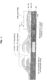
- the positions of the tops of a plurality of bumps having the equal height formed over a multi-layered interconnection layer formed over a semiconductor element may vary and thus may not be located on the same plane, since the surface of the multi-layered interconnection layer is not flat, that is, the surface has steps.
- the positions of the tops of bumps may also vary.
- the bumps contact a mounting board at different times, with the most protruding bumps contacting the first, as depicted in FIG. 13 .
- the force is adjusted such that the least protruding bump is bonded to have an optimal bonding strength, bumps protruding larger than the least protruding bump would undergo excessive force, which results in insufficient bonding strengths.
- the most protruding bump would undergo excessive force, and its bonding strength would become weaker.
- bumps protruding larger than the least protruding bump particularly, the most protruding bump
- undergo excessive force and the vibration generated by the ultrasound is prevented from traveling to such bumps.
- a semiconductor device is provided with protruding metal bumps of at least two widths, the widths of the bumps being selected in accordance with their degree of protrusion.
- a semiconductor device includes: a semiconductor element; a first bump that is located over a surface (top surface) of the semiconductor element, and is formed on a first bump formation face (first plane) distanced from a back surface (opposite surface) of the semiconductor element at a first distance; and a second bump that is located over the surface of the semiconductor element, and is formed on a second bump formation face (second plane) distanced from the back surface of the semiconductor element at a second distance larger than the first distance, the second bump having a diameter larger than that the first bump.
- a method of manufacturing a semiconductor device includes: forming a first bump that is located over a surface of the semiconductor element, on a first bump formation face distanced from a back surface of the semiconductor element at a first distance, and a second bump that is located over the surface of the semiconductor element, on a second bump formation face distanced from the back surface of the semiconductor element at a second distance being longer than the first distance, the second bump having a diameter larger than a diameter of the first bump; and bonding the first and second bumps and a surface electrode of a mounting board together.
- FIGS. 1-11 a semiconductor device and a method of manufacturing the same according to one embodiment will be described with reference to FIGS. 1-11 .
- a semiconductor device is a semiconductor chip 2 including a plurality of bumps 1 (1A-1E), as depicted in FIG. 1 .
- the bumps are generally circular in cross-section so as to have a diameter.
- this semiconductor device is the semiconductor chip 2 having a semiconductor element 3 and the bumps 1 (1A-1E) having different diameters, which are located over the surface of the semiconductor element 3, and are formed over a plurality of bump formation faces or planes 4 (4A-4E) distanced from the back surface 3A of the semiconductor element 3 at varied distances.
- the semiconductor element 3 is sometimes referred to as a "semiconductor device".
- the semiconductor element 3 includes an integrated circuit (not illustrated) and a surface electrode 5.
- the semiconductor element 3 is a semiconductor element, made from a semiconductor material, such as gallium arsenide or silicon, for example.
- the semiconductor chip 2 includes an interconnection layer 7 including at least one conductor layer 6 over the semiconductor element 3.
- the semiconductor chip 2 includes the interconnection layer 7 between the semiconductor element 3 and the bumps 1.
- the bump formation faces 4 are located on the surface of the interconnection layer 7.
- a multi-layered interconnection layer is provided as the interconnection layer 7.
- the interconnection layer 7 also includes an interconnection 6A and an interconnection electrode (via) 6B, as a conductor layer 6, and further includes a protection layer 8 made from a photosensitive polybenzoxazole or photosensitive polyimide, for example.
- the semiconductor chip 2 is a semiconductor chip having a wafer level package (WLP) 9.
- WLP wafer level package
- the wafer level package 9 is also referred to as a wafer level chip size package (WL-CSP) or a chip size package (CSP).
- the semiconductor chip 2 having the wafer level package 9 is formed by forming the interconnection layer 7 including at least one conductor layer 6 at wafer level, followed by dicing the wafer into individual chips.
- the interconnection layer 7 including at least one conductor layer 6 at wafer level
- dicing the wafer into individual chips For example, after forming a multi-layered interconnection layer 7, e.g., a redistribution layer, over the surface electrode 5 of the semiconductor element 3 (wafer) made from a semiconductor material, such as silicon or gallium arsenide, the wafer is diced into individual chips.
- the semiconductor chip 2 having the wafer level package 9 is a semiconductor chip having a package 9 that is equally sized (size-matched) to the chip, over the semiconductor element 3.
- the semiconductor chip 2 having the wafer level package 9 is a semiconductor chip having the interconnection layer 7 including at least one conductor layer 6, as the package 9 that is equally sized to the chip, over the semiconductor element 3.
- each of the bump formation faces 4A-4E is located on the surface of the package 9 (the interconnection layer 7).
- the semiconductor chip 2 having the wafer level package 9 includes the interconnection layer 7 between the semiconductor element 3 and the bumps 1.
- the semiconductor chip 2 including the interconnection layer 7, particularly the wafer level package, the semiconductor chip 2 need not include interconnection layer or wafer level package.
- the semiconductor chip 2 may be a bare chip.
- the bumps 1 are plating bumps (gold plating bumps, in this example) formed with metal plating (gold plating, in this example).
- the bumps 1 are preferably metal bumps including at least gold or copper.
- the bumps I may be stud bumps formed from metal wires.
- metal plating bumps formed with plating are preferred. More specifically, the bumps 1A-1E having different diameters, which will be described later, can be formed economically by forming metal plating bumps using a photolithographically patterned resist.
- the plurality of bumps 1A-1E are formed so as to have the equal height.
- the heights of the bumps 1A-1E may deviate within the tolerable deviation rate of plated bumps.
- the deviation of the heights of the bumps 1A-1E may fall within 10% of the bump height.
- the difference between the height of one bump (first bump), and the height of another bump (second bump) is within 10% of the height of the first bump or the height of the second bump.
- the surface of the semiconductor element 3 or the surface of the interconnection layer 7 formed over the semiconductor element 3 is not flat (has steps), the distances of the plurality of bump formation faces 4A-4E, on which the plurality of bumps 1A-1E are formed, from the back surface 3A of the semiconductor element 3, vary.
- the heights of the bumps 1A-1E is within the tolerable deviation rate of plated bumps, the magnitudes of protrusion of the bumps 1A-1E exceed the tolerable deviation rate of plated bumps.
- the plurality of bumps 1A-1E include, at least two bumps having the difference of the magnitudes of protrusion from the surface 3B of the semiconductor element 3, i.e., the difference of the distances from the surface 3B of the semiconductor element 3 to the tops (the positions of the tops) of the bumps, of larger than 10% of the bump height. Furthermore, the plurality of bumps 1A-1E include, at least two bumps having the difference of the magnitudes of protrusion from the back surface 3A of the semiconductor element 3, i.e., the difference of the distances (device heights) from the back surface 3A of the semiconductor element 3 to the tops (the positions of the tops) of the bumps, of larger than 10% of the bump height.
- the bump formation faces 4A-4E from the back surface 3A the semiconductor element 3 in this embodiment there are five different distances of the bump formation faces 4A-4E from the back surface 3A the semiconductor element 3 in this embodiment, i.e., there are five steps.
- Such distances are grouped into three for the purposes of applying this embodiment of the present invention, and thus the bumps 1A-1E having three different sizes (more specifically widths, or in the case of bumps of circular section, diameters) are formed.
- the distances of the bump formation faces 4A-4E from the back surface 3A of the semiconductor element 3 are grouped into three, and as the distance increases, the corresponding bump diameter is increased in three steps.
- the bumps I D and I C formed on the bump formation faces 4D and 4C, distanced from the back surface 3A of the semiconductor element 3 at the second and third smallest distances will have a diameter larger than that of the bump 1E formed on the bump formation face 4E, the least distanced from the back surface 3A of the semiconductor element 3.
- the bumps 1A and 1B formed on the bump formation faces 4A and 4B, distanced from the back surface 3A of the semiconductor element 3 at the largest and the second largest distances, will have a diameter larger than that of the bumps 1D and 1C formed on the bump formation faces 4D and 4C, distanced from the back surface 3A of the semiconductor element 3 at the second and third smallest distances.
- the bumps 1A-1E are not limited to have circular or oval shapes, and they may have polygon shapes. In such case, the diagonal line of a polygon is used as the bump diameter.
- the above diameters of the bumps 1A-1E are not limiting, and the diameters of the bumps 1A-1E may be varied in accordance with the distances of the bump formation faces 4A-4E from the back surface 3A of the semiconductor element 3, i.e., the magnitudes of protrusion of the bumps 1A-1E.
- the diameters of the plurality of bumps 1A-1E may be increased in accordance with the distance between the back surface 3A of the semiconductor element 3 and the bump formation faces 4A-4E.
- the larger magnitude of protrusion of a bump becomes, the larger the bump diameter may be set.
- the bumps 1A-1E formed on the bump formation faces 4C-4E differently distanced from the back surface 3A of the semiconductor element 3 will have respectively different diameters.
- the diameter of the bump 1A formed on the bump formation face 4A, distanced from the back surface 3A of the semiconductor element 3 at the largest distance may be increased, for example.
- the bumps 1B-1E formed on the bump formation faces 4B-4E other than the bump formation face 4A, distanced from the back surface 3A of the semiconductor element 3 at the largest distance may be formed such that the bumps 1B-1E have the equal diameter and that the diameter of the bump 1A formed on the bump formation face 4A, distanced from the back surface 3A of the semiconductor element 3 at the largest distance, is larger than the bump diameter of the bumps 1B-1E.
- the bumps 1A-1D formed on the bump formation faces 4A-4D other than the bump formation face 4E, distanced from the back surface 3A of the semiconductor element 3 at the smallest distance may be formed such that the bumps 1A-1D have the equal diameter that is larger than the diameter of the bump 1E formed on the bump formation face 4E, distanced from the back surface 3A of the semiconductor element 3 at the smallest distance, for example.
- At least the diameters of bumps having a magnitude of protrusion from the surface 3B of the semiconductor element 3 larger than the magnitude of protrusion obtained by adding the amount corresponding to 10% of the bump height to the magnitude of protrusion of the bump 1E formed on the bump formation face 4E, distanced from the back surface 3A of the semiconductor element 3 at the smallest distance, from the surface 3B of the semiconductor element 3, may be increased, for example.
- At least the diameters of bumps having a distance from the surface 3B of the semiconductor element 3 to the top (the position of the top) of the bump larger than the distance obtained by adding the amount corresponding to 10% of the bump height to the distance of the bump 1E formed on the bump formation face 4E, distanced from the back surface 3A of the semiconductor element 3 at the smallest distance, from the surface 3B of the semiconductor element 3 to the top of the bump, may be increased, for example.
- At least the diameters of bumps having a magnitude of protrusion from the back surface 3A of the semiconductor element 3 larger than the magnitude of protrusion obtained by adding the amount corresponding to 10% of the bump height to the magnitude of protrusion of the bump 1E formed on the bump formation face 4E, distanced from the back surface 3A of the semiconductor element 3 at the smallest distance, from the back surface 3A of the semiconductor element 3, may be increased, for example.
- At least the diameters of bumps having a distance from the back surface 3A of the semiconductor element 3 to the top (the position of the top) of the bump larger than the distance obtained by adding the amount corresponding to 10% of the bump height to the distance of the bump I E formed on the bump formation face 4E, distanced from the back surface 3A of the semiconductor element 3 at the smallest distance, from the back surface 3A of the semiconductor element to the top of the bump, may be increased, for example.
- At least the bump I A formed on the bump formation face 4A, distanced from the back surface 3A of the semiconductor element 3 at the largest distance, may have a diameter larger than those of the other bumps 1B-1E.
- a second bump formed on a second bump formation face which is distanced from the back surface 3A of the semiconductor element 3 at the second distance, may be configured to have a greater diameter than that of a first bump formed on a first bump formation face, which is distanced from the back surface 3A of the semiconductor element 3 at the first distance.
- a third bump formed on a third bump formation face which is distanced from the back surface 3A of the semiconductor element 3 at the third distance, may be configured to have a smaller diameter than that of the first bump.
- the bumps 1 contacting the electrodes of the mounting board ahead of the other bumps are configured to have greater diameters than the other bumps contacting the electrodes of the mounting board later.
- the bump diameters of the bumps are increased according to the time sequence of contact with the corresponding electrode of the mounting board. More specifically, the bump 1A contacting its corresponding electrode of the mounting board first is configured to have a larger diameter than that of the bump 1E contacting its corresponding electrode last.
- the tops (the positions of the tops) of the bumps 1A-1E i.e., the magnitudes of protrusion of the bumps 1A-1E may vary, due to unevenness of the surface of the semiconductor element 3, or the surface of the interconnection layer 7 formed over the semiconductor element 3, and thus the tops (the positions of the tops) of the bumps 1A-1E may not be located on the same plane.
- the bonding heights i.e., the heights from the boundary face between the semiconductor element 3 and the multi-layered interconnection layer 7 to the tops of bumps 1A-1E (i.e., the bonding height to the mounting board), may vary.
- the surface of the semiconductor element 3 or the surface of the interconnection layer 7 formed over the semiconductor element 3 underlies the bumps 1.
- the surface of the semiconductor element 3 or the surface of the interconnection layer 7 formed over the semiconductor element 3 underlying the bumps 1 is not flat (has steps).
- the surface of the interconnection layer 7 becomes uneven since the thickness of the interconnection layer 7 vary across this layer, depending on the number of an interconnection 6A and an interconnection electrode 6B (which are collectively referred to as a "conductor layer") stacked in the respective regions of the interconnection layer 7.
- the thickness of the multi-layered interconnection layer 7 increases around the device, since signal inputs/outputs concentrate around the device, thereby deteriorating the steps (unevenness) of the surface of the multi-layered interconnection layer 7.
- the surface of the semiconductor element 3 becomes uneven due to the variation of the heights of the surface electrodes, for example.
- the bumps contact a mounting board at different times during bonding, with the most protruding bumps contacting the first.
- the force is adjusted such that the least protruding bump is bonded to have an optimal bonding strength, bumps protruding larger than the least protruding bump would undergo excessive force, which results in insufficient bonding strengths.
- a fresh metal face is generated by grinding the bumps 1 and the electrodes of the mounting board under the vibration of the ultrasound, thereby causing metal bond.
- bumps protruding larger than the least protruding bump undergo excessive force and vibration generated by the ultrasound are prevented from traveling to such bumps. This reduces the grinding between the bumps 1 and the electrodes of the mounting board, preventing generation of fresh metal faces. This prevents the bumps protruding larger than the least protruding bump from undergoing metal bond, resulting in insufficient bonding strengths.
- this embodiment varies the diameters of the bumps 1 in accordance with the distances of the bump formation faces 4 from the back surface 3A of the semiconductor element 3, i.e., the magnitudes of protrusion of the bumps 1. Since at least the most protruding bumps 1A undergoes excessive force, among the plurality of bumps 1A-1E, the diameter of at least the bump 1A formed on the bump formation face 4A, distanced from the back surface 3A of the semiconductor element 3 at the largest distance, is set to be larger than the diameters of the other bumps 1B-1E. Thus, the bonding areas of the bumps 1 undergoing excessive force can be increased, thereby increasing the bonding strengths of the bumps 1 undergoing the excessive force.
- the number of bumps 1A-1D for increasing the bump diameter is minimized, i.e., only the diameters of the bumps 1A-1D undergoing excessive force are increased to increase the bonding areas, thereby enhancing the bonding strengths.
- the reliability of the bump bonds across the device is improved by increasing the diameters of the bumps 1A-1D undergoing excessive force.
- semiconductor elements have been provided with an increasing number of terminals while the pitches between the terminals have been narrowed, which renders the strategy of increasing diameters of all bumps disadvantageous.
- a semiconductor device may include a semiconductor chip 2 including above-described plural bumps I and a mounting board 10 including surface electrodes 11, and the surface electrodes 11 of the mounting board 10 and the plurality of bumps 1 of the semiconductor chip 2 may be bonded together, as depicted in FIGS. 2A and 2B . More specifically, a semiconductor device may be such that the semiconductor chip 2 including the plurality of bumps 1 may be mounted on the mounting board 10 by bonding the surface electrodes 11 of the mounting board 10 and the plurality of bumps 1 of the semiconductor chip 2 together.
- under-fill material (resin encapsulation material) 12 may be filled between the semiconductor chip 2 and the mounting board 10, as depicted in FIGS. 2A and 2B . More specifically, after injecting the under-fill material 12 between the semiconductor chip 2 and the mounting board 10, as depicted in FIG. 2A , the under-fill material (under-fill) 12 may be allowed to cure, as depicted in FIGS. 2A and 2B .
- a plurality of bumps 1A-1E are formed over the surface 3B of a semiconductor element 3 (see FIG. 1 ).
- the semiconductor element 3 includes an integrated circuit (not illustrated) and surface electrode 5.
- the semiconductor element 3 is a semiconductor element, made from a semiconductor material, such as gallium arsenide or silicon, for example.
- the surface 3B of the semiconductor element 3 there are a plurality of (five in the drawing) steps (the surface is not flat). More specifically, there are a plurality of (five in the drawing) bump formation faces 4A-4E, that are distanced from the back surface 3A of the semiconductor element 3 at the different distance, over the surface 3B of the semiconductor element 3. On these plural bump formation faces 4A-4E, the bumps 1A-1E having different diameters are formed. In other words, the diameters of the bumps 1 are varied in accordance with the magnitudes of protrusion of the bumps 1, i.e., the distances of the bump formation faces 4 from the back surface 3A of the semiconductor element 3. In this embodiment, only the diameters of the bumps 1 undergoing excessive force are increased.
- the plurality of bumps I are formed with metal plating.
- the bumps 1 are preferably formed using metal including at least gold or copper.
- the bumps 1 may be stud bumps formed from metal wires, for example.
- metal plating bumps formed with plating are preferred.
- a second bump formed on a second bump formation face which is distanced from the back surface 3A of the semiconductor element 3 at the second distance, may be configured to have a larger diameter than that of a first bump formed on a first bump formation face, which is distanced from the back surface 3A of the semiconductor element 3 at the first distance.
- a third bump formed on a third bump formation face which is distanced from the back surface 3A of the semiconductor element 3 at the third distance, may be configured to have a smaller diameter than that of the first bump.
- the semiconductor chip 2 including the plurality of bumps 1 is fabricated (see FIG. 1 ).
- the plurality of bumps 1 of the semiconductor chip 2 and the surface electrodes 11 of the mounting board 10 are bond together (see FIGS. 2A and 2B ).
- the plurality of bumps 1 of the semiconductor chip 2 and the surface electrodes 11 of the mounting board 10 are bonded using ultrasonic bonding.
- the plurality of bumps 1 of the semiconductor chip 2 and the surface electrodes 11 of the mounting board 10 may be bonded together under a force.
- the plurality of bumps 1 of the semiconductor chip 2 and the surface electrodes 11 of the mounting board 10 may be bonded together under a force of approximately 0.05 N or more per bump.
- low-cost bonding techniques utilizing metal bumps of the semiconductor chip 2, e.g., plating bumps and stud bumps
- thermo compression bonding, pressure bonding, and ultrasonic bonding there are thermo compression bonding, pressure bonding, and ultrasonic bonding. All of these bonding techniques apply a force during bonding. Forces applied during thermo compression bonding and pressure bonding range from approximately 0.2 N to about 1 N per bump, while forces applied during ultrasonic bonding range from about 0.05 N to approximately 0.3 N per bump.
- under-fill material (resin encapsulation material) 12 is filled between the semiconductor chip 2 and the mounting board 10 by injecting the under-fill material 12 between the semiconductor chip 2 and the mounting board 10 and allowing it to cure (see FIGS. 2A and 2B ). Note that such a filing step of the under-fill material 12 may be done prior to bonding.
- the semiconductor chip 2 including the plurality of bumps 1 is a semiconductor chip 2 including an interconnection layer 7 including at least one conductor layer 6 (e.g., multi-layered interconnection layer) over the surface of the semiconductor element 3 (see FIG. 1 ), as described previously.
- the bump formation faces 4 are located on the surface of the interconnection layer 7.
- the semiconductor chip 2 including the plurality of bumps I is a semiconductor chip 2 including a wafer level package 9 (see FIG. 1 ), as described previously.
- the bump formation faces 4 are located on the surface of the wafer level package 9 (the interconnection layer 7).
- the interconnection layer 7 also includes an interconnection 6A and an interconnection electrode 6B as a conductor layer 6, and further includes a protection layer 8 including a photosensitive polybenzoxazole or a photosensitive polyimide, for example.
- a method of manufacturing a semiconductor device of the embodiment includes following steps.
- the semiconductor chip 2 including the plurality of bumps 1 is a semiconductor chip 2 including an interconnection layer 7 including at least one conductor layer 6 (e.g., multi-layered interconnection layer) over the surface of a semiconductor element 3, the interconnection layer 7 including at least one conductor layer 6 (e.g., multi-layered interconnection layer) is formed over the semiconductor element 3, before formation of the plurality of bumps 1 over the surface 3B of the semiconductor element 3 (see FIG. 1 ).
- the interconnection layer 7 including at least one conductor layer 6 e.g., multi-layered interconnection layer
- the wafer level package 9 is formed over the semiconductor element 3 in the form of a wafer, before formation of the plurality of bumps 1 over the surface 3B of the semiconductor element 3.
- the wafer level package 9 is formed over the semiconductor element 3 in the form of a wafer by forming an interconnection layer 7 including at least one conductor layer 6 (e.g., multi-layered interconnection layer) at wafer level. In this manner, the semiconductor element 3 in the form of a wafer is converted to the wafer level package 9.
- steps there are a plurality of (five in the drawing) steps (the surface is not flat) on the surface of the interconnection layer 7 formed over the semiconductor element 3 in the above-described steps (see FIG. 1 ). More specifically, there are a plurality of (five in the drawing) bump formation faces 4, that are distanced from the back surface 3A of the semiconductor element 3 at the different distance, over the surface of the interconnection layer 7 formed over the semiconductor element 3.
- the bump formation faces 4 are located on the surface of the interconnection layer 7.
- the bump formation faces 4 are located on the surface of the wafer level package 9 (the interconnection layer 7).
- the semiconductor chip 2 including the plurality of bumps 1 is a semiconductor chip 2 including an interconnection layer 7 including at least one conductor layer 6 over the surface 3B of a semiconductor element 3, the plurality of bumps I having different diameters are formed on the plurality of bump formation surfaces 4 defining a part of the surface of the interconnection layer 7.
- the semiconductor chip 2 including the plurality of bumps 1 is a semiconductor chip 2 including a wafer level package 9, the plurality of bumps 1 having different diameters are formed on the plurality of bump formation surfaces 4 defining a part of the surface of the wafer level package 9 (the interconnection layer 7).
- the semiconductor chip 2 including the plurality of bumps I is a semiconductor chip 2 including a wafer level package 9, by dicing the wafer into individual chips after forming the plurality of bumps I having different diameters on the plurality of bump formation surfaces 4 defining a part of the surface of the wafer level package 9 (the interconnection layer 7), as described above, the semiconductor chip 2 including the plurality of bumps I and the wafer level package 9 is formed (see FIG. 1 ).
- the semiconductor chip 2 having the wafer level package 9 will be mounted on the mounting board 10 by bonding the plurality of bumps 1 of the semiconductor chip 2 having the wafer level package 9 and the surface electrodes 11 of the mounting board 10 together.
- plating bumps 1 are formed over a semiconductor chip 2 including a wafer level package 9
- a plurality of bump formation faces 4 are located on the surface of the wafer level package 9 (the interconnection layer 7).
- a semiconductor element 3 is a gallium arsenide wafer 3X
- a plating bump 1A having the largest diameter is formed on a bump formation face 4A that is distanced from the back surface 3XA of the gallium arsenide wafer 3X at the largest distance
- a plating bump I E having smallest diameter is formed on a bump formation face 4E that is distanced from the back surface 3XA of the gallium arsenide wafer 3X at the smallest distance.
- a protection layer 8X having a thickness of about 3 ⁇ m, for example, and having a via with a diameter of about 15 ⁇ m over the surface electrode 5A is formed, from a photosensitive polybenzoxazole, for example.
- a seed layer having a thickness of about 0.2 ⁇ m, for example is formed, such as by sputtering, using titanium tungsten/gold, for example.
- titanium tungsten/gold refers to sputtering titanium tungsten, followed by sputtering of gold, without breaking vacuum. Any material including a slash "/” refers to a similarly formed material.
- the "thickness of about 0.2 ⁇ m" is the combined thickness of titanium tungsten and gold.
- a gold interconnection (not illustrated) having a film thickness of about 3 ⁇ m and a line width of about 20 ⁇ m, for example, is formed, as a first-level interconnection 6X, using photolithography and electroplating, for example.
- the via in the protection layer 8X over the surface electrode 5A over the gallium arsenide wafer 3X is filled with gold, thereby forming a gold electrode 6XA as an electrode in the first-level interconnection 6X.
- the first-level gold interconnection (not illustrated) and the gold electrode 6XA are collectively referred to as a conductor layer.
- the gold electrode 6XA is referred to as an interconnection electrode (redistribution layer electrode).
- a protection layer 8Y having a thickness of about 3 ⁇ m, for example, and having a via with a diameter of about 15 ⁇ m over the gold electrode 6XA of the first-level interconnection 6X is formed, from a photosensitive polybenzoxazole, for example.
- first-level interconnection layer 7X including the first-level gold interconnection (not illustrated), the gold electrode 6XA, and the protection layers 8X and 8Y, is formed.
- a seed layer having a thickness of about 0.2 ⁇ m, for example, is formed, such as by sputtering, using titanium tungsten/gold, for example.
- a gold interconnection (not illustrated) having a film thickness of about 3 ⁇ m and a line width of about 20 ⁇ m, for example, is formed, as a second-level interconnection 6Y, using photolithography and electroplating, for example.
- the via in the protection layer 8Y over the gold electrode 6XA for the first-level interconnection 6X is filled with gold, thereby forming a gold electrode 6YA as an electrode for the second-level interconnection 6Y.
- a gold electrode 6YB is formed over the surface of the protection layer 8Y over the surface electrode 5B over the gallium arsenide wafer 3X, as an electrode for the second-level interconnection 6Y.
- the second-level gold interconnection (not illustrated) and the gold electrodes 6YA and 6YB are collectively referred to as a conductor layer. Additionally, the gold electrodes 6YA and 6YB are referred to as an interconnection electrode (redistribution layer electrode). Note that the second-level gold electrodes 6YA and 6YB are surface electrodes for a redistribution layer in this embodiment.
- the thicknesses from the back surface (backside) 3XA of the gallium arsenide wafer 3X to the surfaces of the redistribution layer surface electrodes 6YA and 6YB were measured, and the difference between the maximum and minimum thicknesses was about 5 ⁇ m.
- the redistribution layer 7 (the wafer level package 9, dual-layered interconnection layer in this case) is formed over the gallium arsenide wafer 3X.
- the plurality of bump formation faces 4 are located on the surface of the redistribution layer 7, i.e., on the surface of the wafer level package 9.
- the surface of the surface electrode 6YA in the redistribution layer 7 defines a bump formation face 4A that is distanced from the back surface 3XA of the gallium arsenide wafer 3X at the largest distance.
- the surface of the surface electrode 6YB in the redistribution layer 7 defines a bump formation face 4E that is distanced from the back surface 3XA of the gallium arsenide wafer 3X at the smallest distance.
- a seed layer 13 with a thickness of about 0.2 ⁇ m, for example, is formed, such as by sputtering, using titanium tungsten/gold, for example, over the surface of the redistribution layer 7 formed in the processes described above.
- plating bumps 1 are formed over the respective redistribution layer surface electrodes 6YA and 6YB, sandwiching the seed layer 13 therebetween, using photolithography, for example.
- steps for forming a plating bump 1A of the largest diameter and a plating bump 1E of smallest diameter will be illustrated and described.
- a photoresist 14 to be used for formation of plating bumps is formed in a film thickness of about 30 ⁇ m, for example.
- openings 14A and 14B are formed, using the photo mask, by varying the diameter in accordance with the thicknesses from the back surface 3XA of the gallium arsenide wafer 3X to the surfaces of the redistribution layer surface electrodes 6YA and 6YB, i.e., the positions of the bump formation faces 4A and 4E.
- the difference between the maximum and minimum thicknesses from the back surface 3XA of the gallium arsenide wafer 3X to the surfaces of the redistribution layer surface electrodes 6YA and 6YB was about 5 ⁇ m, as described previously.
- an opening 14A having an opening diameter of about 40 ⁇ m is formed over the redistribution layer surface electrode (6YA) which has a difference between the maximum and minimum thicknesses of about 2 ⁇ m.
- the opening 14A having an opening diameter of about 40 ⁇ m is formed over the redistribution layer surface electrode (6YA) which has a thickness from the back surface 3XA of the gallium arsenide wafer 3X to the surface of the redistribution layer surface electrode (6YA) equal to or greater than a certain value.
- an opening 14B having an opening diameter of about 30 ⁇ m is formed over the redistribution layer surface electrode (6YB) which has a thickness between the maximum and minimum thicknesses larger than about 2 ⁇ m.
- the opening 14B having an opening diameter of about 30 ⁇ m is formed over the redistribution layer surface electrode (6YB) which has a thickness from the back surface 3XA of the gallium arsenide wafer 3X to the surface of the redistribution layer surface electrode (6YB) smaller than that certain value.
- gold plating bumps 1A and 1E are formed by electroplating gold, for example, to a thickness of about 25 ⁇ m, for example, using the resist mask 14 having the openings 14A and 14B of different diameter, which has been formed in the processes described above.
- the gold plating bump 1A has a diameter of about 40 ⁇ m and a cross-sectional area of 1256 ⁇ m 2 .
- the gold plating bump 1E has a diameter of about 30 ⁇ m and a cross-sectional area of 706.5 ⁇ m 2 .
- the photoresist 14 is stripped away (removed) as depicted in FIGS. 8A and 8B , the seed layer 13 in the areas other than the areas, in which the gold plating bumps 1A and 1E are formed, is removed by etching, as depicted in FIGS. 9A and 9B . Thereafter, the wafer 3X is diced into individual chips to fabricate a semiconductor chip 2 (gallium arsenide chip) having the plurality of bumps 1 (see FIG. 1 ).
- a semiconductor chip 2 gallium arsenide chip
- a mounting board 10 (resin package board) including gold electrodes 11, as surface electrodes, is provided (see FIGS. 2A and 2B ).
- the plurality of bumps 1 of the semiconductor chip 2 and the surface electrodes 11 of the mounting board 10 fabricated in the processes described above are ultrasonically bonded together to mount the semiconductor chip 2 on the mounting board 10.
- the ultrasonic bonding is performed by applying ultrasound of about 50 kHz for about 1.5 seconds under a force of about 0.1 N per bump.
- the semiconductor device of the first specific example of this embodiment has been fabricated.
- plating bumps 1 are formed over a semiconductor chip 2 including a wafer level package 9
- the plurality of bump formation faces 4 are located on the surface of the wafer level package 9 (the interconnection layer 7).
- a semiconductor element 3 is a silicon wafer
- a plating bump 1A having the largest diameter is formed on a bump formation face 4A that is distanced from the back surface of the silicon wafer at the largest distance
- a plating bump 1E having smallest diameter is formed on a bump formation face 4E that is distanced from the back surface of the silicon wafer at the smallest distance.
- this second specific example is different from the above-described first specific example, primarily in terms of the materials of a wafer (semiconductor element), electrodes, protection layers, seed layers, and the like.
- the steps in this second specific example are similar to those in the above-described first specific example. Accordingly, a wafer (semiconductor element), protection layers, seed layers, and the like, made from different materials are referenced to by the same reference symbols, and will be described with reference to the same drawings.
- a protection layer 8X having a thickness of about 3 ⁇ m, for example, and having a via with a diameter of about 15 ⁇ m over the surface electrode 5A is formed, from a photosensitive polyimide, for example (see FIG. 3B ).
- a seed layer having a thickness of about 0.2 ⁇ m, for example is formed, such as by sputtering, using titanium/copper or titanium tungsten/copper, for example.
- a copper interconnection (not illustrated) having a film thickness of about 5 ⁇ m and a line width of about 20 ⁇ m, for example, is formed, as a first-level interconnection 6X, using photolithography and electroplating, for example (see FIG. 3C ).
- the via in the protection layer 8X over the surface electrode 5A over the silicon wafer 3X is filled with copper, thereby forming a copper electrode 6XA as an electrode in the first-level interconnection 6X.
- the first-level copper interconnection (not illustrated) and the copper electrode 6XA are collectively referred to as a conductor layer.
- the copper electrode 6XA is referred to as an interconnection electrode (redistribution layer electrode).
- a protection layer 8Y having a thickness of about 3 ⁇ m, for example, and having a via with a diameter of about 15 ⁇ m over the copper electrode 6XA of the first-level interconnection 6X is formed, from a photosensitive polyimide, for example (see FIG. 3D ).
- first-level interconnection layer 7X including the first-level copper interconnection (not illustrated), the copper electrode 6XA, and the protection layers 8X and 8Y, is formed.
- a seed layer having a thickness of about 0.2 ⁇ m, for example is formed, such as by sputtering, using titanium/copper or titanium tungsten/copper, for example.
- a copper interconnection (not illustrated) having a film thickness of about 5 ⁇ m and a line width of about 20 ⁇ m, for example, is formed, as a second-level interconnection 6Y, using photolithography and electroplating, for example (see FIG. 4 ).
- the via in the protection layer 8Y over the copper electrode 6XA for the first-level interconnection 6X is filled with copper, thereby forming a copper electrode 6YA as an electrode for the second-level interconnection 6Y.
- a copper electrode 6YB is formed over the surface of the protection layer 8Y over the surface electrode 5B over the silicon wafer 3X, as an electrode for the second-level interconnection 6Y.
- the second-level copper interconnection (not illustrated) and the copper electrodes 6YA and 6YB are collectively referred to as a conductor layer. Additionally, the copper electrodes 6YA and 6YB are referred to as an interconnection electrode (redistribution layer electrode). Note that the second-level copper electrodes 6YA and 6YB are surface electrodes for a redistribution layer in this embodiment.
- the distances from the back surface (backside) 3XA of the silicon wafer 3X to the surfaces of the redistribution layer surface electrodes 6YA and 6YB were measured, and the difference between the maximum and minimum thicknesses was about 5 ⁇ m.
- a protection layer 8Z having a thickness of about 3 ⁇ m, and having vias 8ZA and 8ZB of a diameter of about 40 ⁇ m over the copper electrodes 6YA and 6YB, as the surface electrodes, is formed, from a photosensitive polyimide, for example (see FIGS. 5A and 5B ),
- the redistribution layer 7 (the wafer level package 9, dual-layered interconnection layer in this case) is formed over the silicon wafer 3X.
- the plurality of bump formation faces 4 are located on the surface of the redistribution layer 7, i.e., on the surface of the wafer level package 9.
- the surface of the surface electrode 6YA in the redistribution layer 7 defines a bump formation face 4A that is the most distanced from the back surface 3XA of the silicon wafer 3X at the largest distance.
- the surface of the surface electrode 6YB in the redistribution layer 7 defines a bump formation face 4E that is distanced from the back surface 3XA of the silicon wafer 3X at the smallest distance.
- plating bumps 1 are formed over the respective redistribution layer surface electrodes 6YA and 6YB, sandwiching the seed layer 13 therebetween, using photolithography, for example.
- steps for forming a plating bump 1A of the largest diameter and a plating bump 1E of smallest diameter will be illustrated and described.
- a photoresist 14 to be used for formation of plating bumps is formed in a film thickness of about 30 ⁇ m, for example.
- openings 14A and 14B are formed, using the photo mask, by varying the diameter in accordance with the thicknesses from the back surface 3XA of the silicon wafer 3X to the surfaces of the redistribution layer surface electrodes 6ZY and 6YB, i.e., the positions of the bump formation faces 4A and 4E (see FIGS. 6A and 6B ).
- the difference between the maximum and minimum thicknesses from the back surface 3XA of the silicon wafer 3X to the surfaces of the redistribution layer surface electrodes 6YA and 6YB was about ⁇ m, as described previously.
- an opening 14A having an opening diameter of about 50 ⁇ m is formed over the redistribution layer surface electrode (6YA) which has a difference between the maximum and minimum thicknesses of about 2 ⁇ m.
- the opening 14A having an opening diameter of about 50 ⁇ m is formed over the redistribution layer surface electrode (6YA) which has a thickness from the back surface 3XA of the silicon wafer 3X to the surface of the redistribution layer surface electrode (6YA) equal to or greater than a certain value.
- an opening 14B having an opening diameter of about 40 ⁇ m is formed over the redistribution layer surface electrode (6YB) which has a difference between the maximum and minimum thicknesses larger than about 2 ⁇ m.
- the opening 14B having an opening diameter of about 40 ⁇ m is formed over the redistribution layer surface electrode (6YB) which has a thickness from the back surface 3XA of the silicon wafer 3X to the surface of the redistribution layer surface electrode (6YB) smaller than that certain value.
- gold plating bumps 1 A and 1 E are formed by electroplating gold, for example, to a thickness of about 25 ⁇ m, for example, using the resist mask 14 having the openings 14A and 14B of different diameter, which has been formed in the processes described above (see FIGS. 7A and 7B ).
- the gold plating bump 1A has a diameter of about 50 ⁇ m and a cross-sectional area of 1962.5 ⁇ m 2 .
- the gold plating bump 1E has a diameter of about 40 ⁇ m and a cross-sectional area of 1256 ⁇ m 2 .
- a mounting board 10 (resin package board) including gold electrodes 11, as surface electrodes, is provided (see FIGS. 2A and 2B ).
- the plurality of bumps 1 of the semiconductor chip 2 and the surface electrodes 11 of the mounting board 10 fabricated in the processes described above are ultrasonically bonded together to mount the semiconductor chip 2 on the mounting board 10.
- the ultrasonic bonding is performed by applying ultrasound of about 50 kHz for about 2 seconds under a force of about 0.1 N per bump.
- the semiconductor device of the second specific example of this embodiment has been fabricated.
- a semiconductor device and a method of manufacturing the same of the embodiment have an advantage in that sufficient bonding strength are obtained for all bumps when bonding to a mounting board 10 even when the tops (the positions of the tops) of the bumps 1, i.e., the magnitudes of protrusion of the bumps 1 vary. They also have another advantage of being able to realize a semiconductor device including highly reliable bonds.
- all plating bumps (bump numbers 1-12) provided excellent shear strengths of approximately 0.2 N or more per bump, regardless of the thicknesses from the back surface (chip backside) of a gallium arsenide chip to the surfaces of redistribution layer surface electrodes, i.e., the positions of bump formation faces.
- a semiconductor device of a first comparative example was also manufactured in the manner similar to the first specific example of a method of manufacturing a semiconductor device described above, except that openings having the equal diameter (diameter of about 30 ⁇ m, in this example) were formed in a resist mask 14 to be used for formation of forming plating bumps 1.
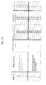
- the shear strengths of the bumps were similarly measured for evaluating the reliability of the semiconductor device of the first comparative example, and the evaluation results listed in FIG. 11 were obtained.
- plating bumps (bump numbers 1-6) formed over redistribution layer surface electrodes, having smaller thicknesses from the back surface of a gallium arsenide chip to the surfaces of redistribution layer surface electrodes, provided excellent shear strengths of approximately 0.2 N or more per bump.
- plating bumps (bump numbers 7-12) formed over the redistribution layer surface electrodes, having larger thicknesses from the back surface of the gallium arsenide chip to the surfaces of redistribution layer surface electrodes, provided only poor shear strengths of approximately 0.13 N or less per bump.
- the bonding areas of the semiconductor device of the first comparative example were measured, and the plating bumps (bump numbers 1-6) formed over the redistribution layer surface electrodes, having smaller thicknesses from the back surface of the gallium arsenide chip to the surfaces of redistribution layer surface electrodes, had bonding areas of about 900 ⁇ m 2 .
- the plating bumps (bump numbers 7-12) formed over the redistribution layer surface electrodes, having larger thicknesses from the back surface of the gallium arsenide chip to the surfaces of redistribution layer surface electrodes had bonding areas of about 400 ⁇ m 2 .
- the plating bumps (bump numbers 7-12) formed over the redistribution layer surface electrodes, having larger thicknesses from the back surface of the gallium arsenide chip to the surfaces of redistribution layer surface electrodes did not provide sufficient shear strengths (bonding strengths) since sufficient bonding areas were not obtained.
- the bonding areas of the semiconductor device of the above-described first specific example were measured, and the plating bumps (bump numbers 1-6) formed over the redistribution layer surface electrodes, having smaller thicknesses from the back surface of the gallium arsenide chip to the surfaces of redistribution layer surface electrodes, had bonding areas of about 900 ⁇ m 2 . Furthermore, the plating bumps (bump numbers 7-12) formed over the redistribution layer surface electrodes, having larger thicknesses from the back surface of the gallium arsenide chip to the surfaces of redistribution layer surface electrodes, had bonding areas of about 1200 ⁇ m 2 .
- the sufficient bonding areas could be obtained by increasing the bump diameters of the plating bumps (bump numbers 7-12) formed over the redistribution layer surface electrodes, having larger thicknesses from the back surface of the gallium arsenide chip to the surfaces of redistribution layer surface electrodes, to about 40 ⁇ m. This resulted in sufficient shear strengths (bonding strengths) for all of the plating bumps (bump numbers 1-12), as described previously.
- the shear strengths of the bumps were measured for evaluating the reliability of a semiconductor device of the above-described second specific example, and all plating bumps provided excellent shear strengths of approximately 0.2 N or more per bump, regardless of the thicknesses from the back surface of a silicon chip to the surfaces of redistribution layer surface electrodes, i.e. the positions of bump formation faces.
- a semiconductor device of a second comparative example was also manufactured in the manner similar to the second specific example of a method of manufacturing a semiconductor device described above, except that openings having the equal diameter (diameter of about 40 ⁇ m, in this example) were formed in a resist mask 14 to be used for formation of forming plating bumps 1.
- the shear strengths of the bumps were measured for evaluating the reliability of the semiconductor device of the second comparative example, and only plating bumps formed over redistribution layer surface electrodes, having smaller thicknesses from the back surface of the silicon chip to the surfaces of redistribution layer surface electrodes, provided excellent shear strengths of approximately 0.2 N or more per bump.
- plating bumps formed over the redistribution layer surface electrodes, having larger thicknesses from the back surface of the silicon chip to the surfaces of redistribution layer surface electrodes provided only poor shear strengths of approximately 0.1 N or less per bump.
Landscapes
- Wire Bonding (AREA)
- Engineering & Computer Science (AREA)
- Manufacturing & Machinery (AREA)
Abstract
Description
- The present invention relates to a semiconductor device and a method of manufacturing the same.
- With downsizing of electronic devices, flip-chip mounting techniques have become widely used, for mounting electronic components, e.g., semiconductor devices, directly on a mounting board, for densely mounting the electronic components.
- As low-cost bonding techniques, there is a technique using metal bumps, e.g., plating bumps and stud bumps formed over semiconductor elements or wafer level packages, and bonding under pressure, for example.
- Now, reference is made to
FIG. 12 . As depicted, in some cases, the positions of the tops of a plurality of bumps having the equal height formed over a multi-layered interconnection layer formed over a semiconductor element, i.e., the magnitudes of protrusion of the bumps, may vary and thus may not be located on the same plane, since the surface of the multi-layered interconnection layer is not flat, that is, the surface has steps. Similarly, when the plurality of bumps having equal height are formed over a semiconductor element without having a multi-layered interconnection layer between the semiconductor element and the bumps, the positions of the tops of bumps may also vary. - In such a case, during bonding, the bumps contact a mounting board at different times, with the most protruding bumps contacting the first, as depicted in
FIG. 13 . During bonding to a mounting board under a pressing force, if the force is adjusted such that the least protruding bump is bonded to have an optimal bonding strength, bumps protruding larger than the least protruding bump would undergo excessive force, which results in insufficient bonding strengths. Particularly, the most protruding bump would undergo excessive force, and its bonding strength would become weaker. - For example, in ultrasonic bonding, bumps protruding larger than the least protruding bump, particularly, the most protruding bump, undergo excessive force and the vibration generated by the ultrasound is prevented from traveling to such bumps. This reduces the grinding between bumps and the electrodes of the mounting board, preventing generation of fresh metal faces. This prevents the bumps protruding larger than the least protruding bump, especially, the most protruding bump, from undergoing metal bond, resulting in weaker bonding strengths, causing insufficient bonding strengths.
- Therefore, obtaining sufficient bonding strengths for all bumps is desired when bonding to a mounting board even in the case where the positions of the tops of the bumps , i.e., the magnitudes of protrusion of the bumps, vary.
- According to the present invention a semiconductor device is provided with protruding metal bumps of at least two widths, the widths of the bumps being selected in accordance with their degree of protrusion.
- According to an aspect of the embodiment, a semiconductor device includes: a semiconductor element; a first bump that is located over a surface (top surface) of the semiconductor element, and is formed on a first bump formation face (first plane) distanced from a back surface (opposite surface) of the semiconductor element at a first distance; and a second bump that is located over the surface of the semiconductor element, and is formed on a second bump formation face (second plane) distanced from the back surface of the semiconductor element at a second distance larger than the first distance, the second bump having a diameter larger than that the first bump.
- According to another aspect of the embodiment, a method of manufacturing a semiconductor device includes: forming a first bump that is located over a surface of the semiconductor element, on a first bump formation face distanced from a back surface of the semiconductor element at a first distance, and a second bump that is located over the surface of the semiconductor element, on a second bump formation face distanced from the back surface of the semiconductor element at a second distance being longer than the first distance, the second bump having a diameter larger than a diameter of the first bump; and bonding the first and second bumps and a surface electrode of a mounting board together.
- Reference is made, by way of example only, to the accompanying drawings in which:
-
FIG. 1 is a schematic cross-sectional view illustrating the structure of a semiconductor device (semiconductor chip) according to one embodiment; -
FIGS. 2A and 2B are schematic cross-sectional views illustrating the structure of a semiconductor device (having a semiconductor chip is mounted on a mounting board) according to one embodiment, and a method of manufacturing the same; -
FIGS. 3A-3D are schematic cross-sectional views illustrating a first specific example of a method of manufacturing a semiconductor device according to one embodiment; -
FIG. 4 is a schematic cross-sectional view illustrating the first specific example of a method of manufacturing a semiconductor device according to one embodiment; -
FIGS. 5A-5D are schematic cross-sectional views illustrating the first specific example of a method of manufacturing a semiconductor device according to one embodiment; -
FIGS. 6A and 6B are schematic cross-sectional views illustrating the first specific example of a method of manufacturing a semiconductor device according to one embodiment; -
FIGS. 7A and 7B are schematic cross-sectional views illustrating the first specific example of a method of manufacturing a semiconductor device according to one embodiment; -
FIGS. 8A and 8B are schematic cross-sectional views illustrating the first specific example of a method of manufacturing a semiconductor device according to one embodiment; -
FIGS. 9A and 9B are schematic cross-sectional views illustrating the first specific example of a method of manufacturing a semiconductor device according to one embodiment; -
FIG. 10 is a diagram illustrating results of a reliability evaluation of a semiconductor device manufactured with the first specific example of a method of manufacturing a semiconductor device according to one embodiment; -
FIG. 11 is a diagram illustrating results of a reliability evaluation of a semiconductor device manufactured with a comparative example of the first specific example of a method of manufacturing a semiconductor device according to one embodiment; -
FIG. 12 is a schematic cross-sectional view illustrating the problems of the embodiment; and -
FIG. 13 is a schematic view illustrating the problems of the embodiment. - Hereinafter, a semiconductor device and a method of manufacturing the same according to one embodiment will be described with reference to
FIGS. 1-11 . - A semiconductor device according to one embodiment is a
semiconductor chip 2 including a plurality of bumps 1 (1A-1E), as depicted inFIG. 1 . In this example the bumps are generally circular in cross-section so as to have a diameter. More specifically, this semiconductor device is thesemiconductor chip 2 having asemiconductor element 3 and the bumps 1 (1A-1E) having different diameters, which are located over the surface of thesemiconductor element 3, and are formed over a plurality of bump formation faces or planes 4 (4A-4E) distanced from theback surface 3A of thesemiconductor element 3 at varied distances. Note that thesemiconductor element 3 is sometimes referred to as a "semiconductor device". - The
semiconductor element 3 includes an integrated circuit (not illustrated) and asurface electrode 5. Thesemiconductor element 3 is a semiconductor element, made from a semiconductor material, such as gallium arsenide or silicon, for example. - In this embodiment, the
semiconductor chip 2 includes aninterconnection layer 7 including at least oneconductor layer 6 over thesemiconductor element 3. In other words, thesemiconductor chip 2 includes theinterconnection layer 7 between thesemiconductor element 3 and thebumps 1. Thus, thebump formation faces 4 are located on the surface of theinterconnection layer 7. In this embodiment, a multi-layered interconnection layer is provided as theinterconnection layer 7. Theinterconnection layer 7 also includes aninterconnection 6A and an interconnection electrode (via) 6B, as aconductor layer 6, and further includes aprotection layer 8 made from a photosensitive polybenzoxazole or photosensitive polyimide, for example. - In this embodiment, the
semiconductor chip 2 is a semiconductor chip having a wafer level package (WLP) 9. Note that thewafer level package 9 is also referred to as a wafer level chip size package (WL-CSP) or a chip size package (CSP). - Here, the
semiconductor chip 2 having thewafer level package 9 is formed by forming theinterconnection layer 7 including at least oneconductor layer 6 at wafer level, followed by dicing the wafer into individual chips. For example, after forming amulti-layered interconnection layer 7, e.g., a redistribution layer, over thesurface electrode 5 of the semiconductor element 3 (wafer) made from a semiconductor material, such as silicon or gallium arsenide, the wafer is diced into individual chips. - Accordingly, the
semiconductor chip 2 having thewafer level package 9 is a semiconductor chip having apackage 9 that is equally sized (size-matched) to the chip, over thesemiconductor element 3. In other words, thesemiconductor chip 2 having thewafer level package 9 is a semiconductor chip having theinterconnection layer 7 including at least oneconductor layer 6, as thepackage 9 that is equally sized to the chip, over thesemiconductor element 3. In such a case, each of the bump formation faces 4A-4E is located on the surface of the package 9 (the interconnection layer 7). Thus, thesemiconductor chip 2 having thewafer level package 9 includes theinterconnection layer 7 between thesemiconductor element 3 and thebumps 1. - Although reference is made to the
semiconductor chip 2 including theinterconnection layer 7, particularly the wafer level package, thesemiconductor chip 2 need not include interconnection layer or wafer level package. For example, thesemiconductor chip 2 may be a bare chip. - The
bumps 1 are plating bumps (gold plating bumps, in this example) formed with metal plating (gold plating, in this example). Note that thebumps 1 are preferably metal bumps including at least gold or copper. For example, the bumps I may be stud bumps formed from metal wires. For forming bumps with different sizes economically, metal plating bumps formed with plating are preferred. More specifically, thebumps 1A-1E having different diameters, which will be described later, can be formed economically by forming metal plating bumps using a photolithographically patterned resist. - The plurality of
bumps 1A-1E are formed so as to have the equal height. However, the heights of thebumps 1A-1E may deviate within the tolerable deviation rate of plated bumps. For example, the deviation of the heights of thebumps 1A-1E may fall within 10% of the bump height. In such a case, the difference between the height of one bump (first bump), and the height of another bump (second bump) is within 10% of the height of the first bump or the height of the second bump. - In contrast, since the surface of the
semiconductor element 3 or the surface of theinterconnection layer 7 formed over thesemiconductor element 3 is not flat (has steps), the distances of the plurality of bump formation faces 4A-4E, on which the plurality ofbumps 1A-1E are formed, from theback surface 3A of thesemiconductor element 3, vary. Thus, even if the heights of thebumps 1A-1E is within the tolerable deviation rate of plated bumps, the magnitudes of protrusion of thebumps 1A-1E exceed the tolerable deviation rate of plated bumps. That is, the plurality ofbumps 1A-1E include, at least two bumps having the difference of the magnitudes of protrusion from thesurface 3B of thesemiconductor element 3, i.e., the difference of the distances from thesurface 3B of thesemiconductor element 3 to the tops (the positions of the tops) of the bumps, of larger than 10% of the bump height. Furthermore, the plurality ofbumps 1A-1E include, at least two bumps having the difference of the magnitudes of protrusion from theback surface 3A of thesemiconductor element 3, i.e., the difference of the distances (device heights) from theback surface 3A of thesemiconductor element 3 to the tops (the positions of the tops) of the bumps, of larger than 10% of the bump height. - There are five different distances of the bump formation faces 4A-4E from the
back surface 3A thesemiconductor element 3 in this embodiment, i.e., there are five steps. Such distances are grouped into three for the purposes of applying this embodiment of the present invention, and thus thebumps 1A-1E having three different sizes (more specifically widths, or in the case of bumps of circular section, diameters) are formed. In other words, the distances of the bump formation faces 4A-4E from theback surface 3A of thesemiconductor element 3 are grouped into three, and as the distance increases, the corresponding bump diameter is increased in three steps. In such a case, the bumps I D and I C formed on the bump formation faces 4D and 4C, distanced from theback surface 3A of thesemiconductor element 3 at the second and third smallest distances, will have a diameter larger than that of thebump 1E formed on the bump formation face 4E, the least distanced from theback surface 3A of thesemiconductor element 3. Thebumps back surface 3A of thesemiconductor element 3 at the largest and the second largest distances, will have a diameter larger than that of thebumps back surface 3A of thesemiconductor element 3 at the second and third smallest distances. Note that thebumps 1A-1E are not limited to have circular or oval shapes, and they may have polygon shapes. In such case, the diagonal line of a polygon is used as the bump diameter. - The above diameters of the
bumps 1A-1E are not limiting, and the diameters of thebumps 1A-1E may be varied in accordance with the distances of the bump formation faces 4A-4E from theback surface 3A of thesemiconductor element 3, i.e., the magnitudes of protrusion of thebumps 1A-1E. - For example, the diameters of the plurality of
bumps 1A-1E may be increased in accordance with the distance between theback surface 3A of thesemiconductor element 3 and the bump formation faces 4A-4E. In other words, the larger magnitude of protrusion of a bump becomes, the larger the bump diameter may be set. In such a case, thebumps 1A-1E formed on the bump formation faces 4C-4E differently distanced from theback surface 3A of thesemiconductor element 3 will have respectively different diameters. - Alternatively, only the diameter of the
bump 1A formed on thebump formation face 4A, distanced from theback surface 3A of thesemiconductor element 3 at the largest distance, may be increased, for example. In other words, thebumps 1B-1E formed on the bump formation faces 4B-4E other than thebump formation face 4A, distanced from theback surface 3A of thesemiconductor element 3 at the largest distance, may be formed such that thebumps 1B-1E have the equal diameter and that the diameter of thebump 1A formed on thebump formation face 4A, distanced from theback surface 3A of thesemiconductor element 3 at the largest distance, is larger than the bump diameter of thebumps 1B-1E. - Alternatively, the
bumps 1A-1D formed on the bump formation faces 4A-4D other than the bump formation face 4E, distanced from theback surface 3A of thesemiconductor element 3 at the smallest distance, may be formed such that thebumps 1A-1D have the equal diameter that is larger than the diameter of thebump 1E formed on the bump formation face 4E, distanced from theback surface 3A of thesemiconductor element 3 at the smallest distance, for example. - Alternatively, at least the diameters of bumps having a magnitude of protrusion from the
surface 3B of thesemiconductor element 3 larger than the magnitude of protrusion obtained by adding the amount corresponding to 10% of the bump height to the magnitude of protrusion of thebump 1E formed on the bump formation face 4E, distanced from theback surface 3A of thesemiconductor element 3 at the smallest distance, from thesurface 3B of thesemiconductor element 3, may be increased, for example. In other words, at least the diameters of bumps having a distance from thesurface 3B of thesemiconductor element 3 to the top (the position of the top) of the bump larger than the distance obtained by adding the amount corresponding to 10% of the bump height to the distance of thebump 1E formed on the bump formation face 4E, distanced from theback surface 3A of thesemiconductor element 3 at the smallest distance, from thesurface 3B of thesemiconductor element 3 to the top of the bump, may be increased, for example. - Alternatively, at least the diameters of bumps having a magnitude of protrusion from the
back surface 3A of thesemiconductor element 3 larger than the magnitude of protrusion obtained by adding the amount corresponding to 10% of the bump height to the magnitude of protrusion of thebump 1E formed on the bump formation face 4E, distanced from theback surface 3A of thesemiconductor element 3 at the smallest distance, from theback surface 3A of thesemiconductor element 3, may be increased, for example. In other words, at least the diameters of bumps having a distance from theback surface 3A of thesemiconductor element 3 to the top (the position of the top) of the bump larger than the distance obtained by adding the amount corresponding to 10% of the bump height to the distance of the bump I E formed on the bump formation face 4E, distanced from theback surface 3A of thesemiconductor element 3 at the smallest distance, from theback surface 3A of the semiconductor element to the top of the bump, may be increased, for example. - As described above, among the plurality of
bumps 1A-1E, at least the bump I A formed on thebump formation face 4A, distanced from theback surface 3A of thesemiconductor element 3 at the largest distance, may have a diameter larger than those of theother bumps 1B-1E. - In short, assuming that a second distance is longer than a first distance, for increasing bonding areas, a second bump formed on a second bump formation face, which is distanced from the
back surface 3A of thesemiconductor element 3 at the second distance, may be configured to have a greater diameter than that of a first bump formed on a first bump formation face, which is distanced from theback surface 3A of thesemiconductor element 3 at the first distance. Furthermore, assuming that a third distance is shorter than the first distance, a third bump formed on a third bump formation face, which is distanced from theback surface 3A of thesemiconductor element 3 at the third distance, may be configured to have a smaller diameter than that of the first bump. - In this manner, for bonding of the
bumps 1 of thesemiconductor chip 2 and the electrodes of the mounting board, thebumps 1 contacting the electrodes of the mounting board ahead of the other bumps are configured to have greater diameters than the other bumps contacting the electrodes of the mounting board later. In this embodiment, for bonding of thebumps 1 of thesemiconductor chip 2 and the electrodes of the mounting board, the bump diameters of the bumps are increased according to the time sequence of contact with the corresponding electrode of the mounting board. More specifically, thebump 1A contacting its corresponding electrode of the mounting board first is configured to have a larger diameter than that of thebump 1E contacting its corresponding electrode last. - The reason why the diameters of the
bumps 1A-1E are varied in accordance with the distances of the bump formation faces 4A-4E from theback surface 3A of thesemiconductor element 3, i.e., the magnitudes of protrusion of thebumps 1A-1E, will be described. - If a plurality of
bumps 1A-1E having the equal height are formed over asemiconductor element 3 for mounting asemiconductor chip 2 including the plurality ofbumps 1A-1E on a mounting board, the tops (the positions of the tops) of thebumps 1A-1E, i.e., the magnitudes of protrusion of thebumps 1A-1E may vary, due to unevenness of the surface of thesemiconductor element 3, or the surface of theinterconnection layer 7 formed over thesemiconductor element 3, and thus the tops (the positions of the tops) of thebumps 1A-1E may not be located on the same plane. For example, in asemiconductor chip 2 including amulti-layered interconnection layer 7 between thesemiconductor element 3 and thebumps 1A-1E, the bonding heights, i.e., the heights from the boundary face between thesemiconductor element 3 and themulti-layered interconnection layer 7 to the tops ofbumps 1A-1E (i.e., the bonding height to the mounting board), may vary. - Since the
bumps 1 are formed over the surface of thesemiconductor element 3 or the surface of theinterconnection layer 7 formed over thesemiconductor element 3, the surface of thesemiconductor element 3 or the surface of theinterconnection layer 7 formed over thesemiconductor element 3 underlies thebumps 1. The surface of thesemiconductor element 3 or the surface of theinterconnection layer 7 formed over thesemiconductor element 3 underlying thebumps 1 is not flat (has steps). For example, for asemiconductor chip 2 including theinterconnection layer 7, e.g., a multi-layered interconnection layer, such as thesemiconductor chip 2 having awafer level package 9, the surface of theinterconnection layer 7 becomes uneven since the thickness of theinterconnection layer 7 vary across this layer, depending on the number of aninterconnection 6A and aninterconnection electrode 6B (which are collectively referred to as a "conductor layer") stacked in the respective regions of theinterconnection layer 7. Especially in the case where thesemiconductor element 3 is a high-frequency device made from gallium arsenide or the like, for example, the thickness of themulti-layered interconnection layer 7 increases around the device, since signal inputs/outputs concentrate around the device, thereby deteriorating the steps (unevenness) of the surface of themulti-layered interconnection layer 7. In addition, for asemiconductor chip 2 of a bare chip, for example, the surface of thesemiconductor element 3 becomes uneven due to the variation of the heights of the surface electrodes, for example. - As described above, if the tops (the positions of the tops) of the
bumps 1A-1E vary, the bumps contact a mounting board at different times during bonding, with the most protruding bumps contacting the first. During bonding to a mounting board under a force (under pressure), if the force is adjusted such that the least protruding bump is bonded to have an optimal bonding strength, bumps protruding larger than the least protruding bump would undergo excessive force, which results in insufficient bonding strengths. - For example, in an ultrasonic bonding in which bonding is carried out under application of a force and ultrasound, a fresh metal face is generated by grinding the
bumps 1 and the electrodes of the mounting board under the vibration of the ultrasound, thereby causing metal bond. During such an ultrasonic bonding, bumps protruding larger than the least protruding bump undergo excessive force and vibration generated by the ultrasound are prevented from traveling to such bumps. This reduces the grinding between thebumps 1 and the electrodes of the mounting board, preventing generation of fresh metal faces. This prevents the bumps protruding larger than the least protruding bump from undergoing metal bond, resulting in insufficient bonding strengths. - To address varied excessive forces depending on the magnitudes of protrusion of the bumps I, this embodiment varies the diameters of the
bumps 1 in accordance with the distances of the bump formation faces 4 from theback surface 3A of thesemiconductor element 3, i.e., the magnitudes of protrusion of thebumps 1. Since at least the mostprotruding bumps 1A undergoes excessive force, among the plurality ofbumps 1A-1E, the diameter of at least thebump 1A formed on thebump formation face 4A, distanced from theback surface 3A of thesemiconductor element 3 at the largest distance, is set to be larger than the diameters of theother bumps 1B-1E. Thus, the bonding areas of thebumps 1 undergoing excessive force can be increased, thereby increasing the bonding strengths of thebumps 1 undergoing the excessive force. - In this embodiment, the number of
bumps 1A-1D for increasing the bump diameter is minimized, i.e., only the diameters of thebumps 1A-1D undergoing excessive force are increased to increase the bonding areas, thereby enhancing the bonding strengths. In other words, the reliability of the bump bonds across the device is improved by increasing the diameters of thebumps 1A-1D undergoing excessive force. It is also possible to increase diameters of all bumps, rather than increasing the diameters of selected bumps. In recent years, however, semiconductor elements have been provided with an increasing number of terminals while the pitches between the terminals have been narrowed, which renders the strategy of increasing diameters of all bumps disadvantageous. - Although the semiconductor device of this embodiment has been described in the context of a
semiconductor chip 2 including a plurality ofbumps 1A-1E, this is not limiting. For example, a semiconductor device may include asemiconductor chip 2 including above-described plural bumps I and a mountingboard 10 includingsurface electrodes 11, and thesurface electrodes 11 of the mountingboard 10 and the plurality ofbumps 1 of thesemiconductor chip 2 may be bonded together, as depicted inFIGS. 2A and 2B . More specifically, a semiconductor device may be such that thesemiconductor chip 2 including the plurality ofbumps 1 may be mounted on the mountingboard 10 by bonding thesurface electrodes 11 of the mountingboard 10 and the plurality ofbumps 1 of thesemiconductor chip 2 together. In such a case, for reinforcing the connections after the bonding, under-fill material (resin encapsulation material) 12 may be filled between thesemiconductor chip 2 and the mountingboard 10, as depicted inFIGS. 2A and 2B . More specifically, after injecting the under-fill material 12 between thesemiconductor chip 2 and the mountingboard 10, as depicted inFIG. 2A , the under-fill material (under-fill) 12 may be allowed to cure, as depicted inFIGS. 2A and 2B . - Next, a method of manufacturing a semiconductor device according to this embodiment will be described.
- Initially, a plurality of
bumps 1A-1E are formed over thesurface 3B of a semiconductor element 3 (seeFIG. 1 ). - Here, the
semiconductor element 3 includes an integrated circuit (not illustrated) andsurface electrode 5. Thesemiconductor element 3 is a semiconductor element, made from a semiconductor material, such as gallium arsenide or silicon, for example. - Over the
surface 3B of thesemiconductor element 3, there are a plurality of (five in the drawing) steps (the surface is not flat). More specifically, there are a plurality of (five in the drawing) bump formation faces 4A-4E, that are distanced from theback surface 3A of thesemiconductor element 3 at the different distance, over thesurface 3B of thesemiconductor element 3. On these plural bump formation faces 4A-4E, thebumps 1A-1E having different diameters are formed. In other words, the diameters of thebumps 1 are varied in accordance with the magnitudes of protrusion of thebumps 1, i.e., the distances of the bump formation faces 4 from theback surface 3A of thesemiconductor element 3. In this embodiment, only the diameters of thebumps 1 undergoing excessive force are increased. In this embodiment, the plurality of bumps I are formed with metal plating. Note that thebumps 1 are preferably formed using metal including at least gold or copper. Alternatively, thebumps 1 may be stud bumps formed from metal wires, for example. For forming the bumps I with different diameters economically, metal plating bumps formed with plating are preferred. - Assuming that a second distance is longer than a first distance, for increasing bonding areas, a second bump formed on a second bump formation face, which is distanced from the
back surface 3A of thesemiconductor element 3 at the second distance, may be configured to have a larger diameter than that of a first bump formed on a first bump formation face, which is distanced from theback surface 3A of thesemiconductor element 3 at the first distance. Furthermore, assuming that a third distance is shorter than the first distance, a third bump formed on a third bump formation face, which is distanced from theback surface 3A of thesemiconductor element 3 at the third distance, may be configured to have a smaller diameter than that of the first bump. - In this manner, the
semiconductor chip 2 including the plurality of bumps 1 (semiconductor device) is fabricated (seeFIG. 1 ). - Subsequently, the plurality of
bumps 1 of thesemiconductor chip 2 and thesurface electrodes 11 of the mountingboard 10 are bond together (seeFIGS. 2A and 2B ). - In this embodiment, the plurality of
bumps 1 of thesemiconductor chip 2 and thesurface electrodes 11 of the mountingboard 10 are bonded using ultrasonic bonding. - Note that the plurality of
bumps 1 of thesemiconductor chip 2 and thesurface electrodes 11 of the mountingboard 10 may be bonded together under a force. Specifically, the plurality ofbumps 1 of thesemiconductor chip 2 and thesurface electrodes 11 of the mountingboard 10 may be bonded together under a force of approximately 0.05 N or more per bump. For example, as low-cost bonding techniques utilizing metal bumps of thesemiconductor chip 2, e.g., plating bumps and stud bumps, there are thermo compression bonding, pressure bonding, and ultrasonic bonding. All of these bonding techniques apply a force during bonding. Forces applied during thermo compression bonding and pressure bonding range from approximately 0.2 N to about 1 N per bump, while forces applied during ultrasonic bonding range from about 0.05 N to approximately 0.3 N per bump. - Thereafter, under-fill material (resin encapsulation material) 12 is filled between the
semiconductor chip 2 and the mountingboard 10 by injecting the under-fill material 12 between thesemiconductor chip 2 and the mountingboard 10 and allowing it to cure (seeFIGS. 2A and 2B ). Note that such a filing step of the under-fill material 12 may be done prior to bonding. - In this embodiment, the
semiconductor chip 2 including the plurality ofbumps 1 is asemiconductor chip 2 including aninterconnection layer 7 including at least one conductor layer 6 (e.g., multi-layered interconnection layer) over the surface of the semiconductor element 3 (seeFIG. 1 ), as described previously. In such a case, the bump formation faces 4 are located on the surface of theinterconnection layer 7. - Especially, in this embodiment, the
semiconductor chip 2 including the plurality of bumps I is asemiconductor chip 2 including a wafer level package 9 (seeFIG. 1 ), as described previously. In such a case, the bump formation faces 4 are located on the surface of the wafer level package 9 (the interconnection layer 7). - The
interconnection layer 7 also includes aninterconnection 6A and aninterconnection electrode 6B as aconductor layer 6, and further includes aprotection layer 8 including a photosensitive polybenzoxazole or a photosensitive polyimide, for example. - In such case, a method of manufacturing a semiconductor device of the embodiment includes following steps.
- If the
semiconductor chip 2 including the plurality ofbumps 1 is asemiconductor chip 2 including aninterconnection layer 7 including at least one conductor layer 6 (e.g., multi-layered interconnection layer) over the surface of asemiconductor element 3, theinterconnection layer 7 including at least one conductor layer 6 (e.g., multi-layered interconnection layer) is formed over thesemiconductor element 3, before formation of the plurality ofbumps 1 over thesurface 3B of the semiconductor element 3 (seeFIG. 1 ). - Alternatively, if the
semiconductor chip 2 including the plurality ofbumps 1 is asemiconductor chip 2 including awafer level package 9, thewafer level package 9 is formed over thesemiconductor element 3 in the form of a wafer, before formation of the plurality ofbumps 1 over thesurface 3B of thesemiconductor element 3. In other words, thewafer level package 9 is formed over thesemiconductor element 3 in the form of a wafer by forming aninterconnection layer 7 including at least one conductor layer 6 (e.g., multi-layered interconnection layer) at wafer level. In this manner, thesemiconductor element 3 in the form of a wafer is converted to thewafer level package 9. - There are a plurality of (five in the drawing) steps (the surface is not flat) on the surface of the
interconnection layer 7 formed over thesemiconductor element 3 in the above-described steps (seeFIG. 1 ). More specifically, there are a plurality of (five in the drawing) bump formation faces 4, that are distanced from theback surface 3A of thesemiconductor element 3 at the different distance, over the surface of theinterconnection layer 7 formed over thesemiconductor element 3. - In the case of a
semiconductor chip 2 having aninterconnection layer 7 including at least oneconductor layer 6 over thesurface 3B of thesemiconductor element 3, the bump formation faces 4 are located on the surface of theinterconnection layer 7. Especially in the case of asemiconductor chip 2 including awafer level package 9, the bump formation faces 4 are located on the surface of the wafer level package 9 (the interconnection layer 7). - Accordingly, if the
semiconductor chip 2 including the plurality ofbumps 1 is asemiconductor chip 2 including aninterconnection layer 7 including at least oneconductor layer 6 over thesurface 3B of asemiconductor element 3, the plurality of bumps I having different diameters are formed on the plurality of bump formation surfaces 4 defining a part of the surface of theinterconnection layer 7. Alternatively, if thesemiconductor chip 2 including the plurality ofbumps 1 is asemiconductor chip 2 including awafer level package 9, the plurality ofbumps 1 having different diameters are formed on the plurality of bump formation surfaces 4 defining a part of the surface of the wafer level package 9 (the interconnection layer 7). - If the
semiconductor chip 2 including the plurality of bumps I is asemiconductor chip 2 including awafer level package 9, by dicing the wafer into individual chips after forming the plurality of bumps I having different diameters on the plurality of bump formation surfaces 4 defining a part of the surface of the wafer level package 9 (the interconnection layer 7), as described above, thesemiconductor chip 2 including the plurality of bumps I and thewafer level package 9 is formed (seeFIG. 1 ). In such a case, thesemiconductor chip 2 having thewafer level package 9 will be mounted on the mountingboard 10 by bonding the plurality ofbumps 1 of thesemiconductor chip 2 having thewafer level package 9 and thesurface electrodes 11 of the mountingboard 10 together. - Hereinafter, a first specific example of a method of manufacturing a semiconductor device of the embodiment will be described with reference to
FIGS. 3-9 . - Here, an example in which plating bumps 1 are formed over a
semiconductor chip 2 including awafer level package 9 will be explained. In such a case, a plurality of bump formation faces 4 are located on the surface of the wafer level package 9 (the interconnection layer 7). This example will be described in the context in which asemiconductor element 3 is agallium arsenide wafer 3X, aplating bump 1A having the largest diameter is formed on abump formation face 4A that is distanced from the back surface 3XA of thegallium arsenide wafer 3X at the largest distance, and a plating bump I E having smallest diameter is formed on abump formation face 4E that is distanced from the back surface 3XA of thegallium arsenide wafer 3X at the smallest distance. - Initially, as depicted in
FIG. 3A , an about 0.4-mm-thick gallium arsenide wafer (semiconductor element) 3X having an integrated circuit (not illustrated) andsurface electrodes - Subsequently, as depicted in
FIG. 3B , over thegallium arsenide wafer 3X, aprotection layer 8X having a thickness of about 3 µm, for example, and having a via with a diameter of about 15 µm over thesurface electrode 5A is formed, from a photosensitive polybenzoxazole, for example. - Subsequently, although not illustrated, a seed layer having a thickness of about 0.2 µm, for example, is formed, such as by sputtering, using titanium tungsten/gold, for example. As used herein, the "titanium tungsten/gold" refers to sputtering titanium tungsten, followed by sputtering of gold, without breaking vacuum. Any material including a slash "/" refers to a similarly formed material. In addition, the "thickness of about 0.2 µm" is the combined thickness of titanium tungsten and gold.
- Thereafter, as depicted in
FIG. 3C , a gold interconnection (not illustrated) having a film thickness of about 3 µm and a line width of about 20 µm, for example, is formed, as a first-level interconnection 6X, using photolithography and electroplating, for example. In this step, the via in theprotection layer 8X over thesurface electrode 5A over thegallium arsenide wafer 3X is filled with gold, thereby forming a gold electrode 6XA as an electrode in the first-level interconnection 6X.Note that the first-level gold interconnection (not illustrated) and the gold electrode 6XA are collectively referred to as a conductor layer. Additionally, the gold electrode 6XA is referred to as an interconnection electrode (redistribution layer electrode). - Again, as depicted in
FIG. 3D , aprotection layer 8Y having a thickness of about 3 µm, for example, and having a via with a diameter of about 15 µm over the gold electrode 6XA of the first-level interconnection 6X is formed, from a photosensitive polybenzoxazole, for example. - Thereby, a first-
level interconnection layer 7X including the first-level gold interconnection (not illustrated), the gold electrode 6XA, and the protection layers 8X and 8Y, is formed. - Subsequently, although not illustrated, a seed layer having a thickness of about 0.2 µm, for example, is formed, such as by sputtering, using titanium tungsten/gold, for example.
- Thereafter, as depicted in
FIG. 4 , a gold interconnection (not illustrated) having a film thickness of about 3 µm and a line width of about 20 µm, for example, is formed, as a second-level interconnection 6Y, using photolithography and electroplating, for example. In this step, the via in theprotection layer 8Y over the gold electrode 6XA for the first-level interconnection 6X is filled with gold, thereby forming a gold electrode 6YA as an electrode for the second-level interconnection 6Y. In addition, a gold electrode 6YB is formed over the surface of theprotection layer 8Y over thesurface electrode 5B over thegallium arsenide wafer 3X, as an electrode for the second-level interconnection 6Y. Note that the second-level gold interconnection (not illustrated) and the gold electrodes 6YA and 6YB are collectively referred to as a conductor layer. Additionally, the gold electrodes 6YA and 6YB are referred to as an interconnection electrode (redistribution layer electrode). Note that the second-level gold electrodes 6YA and 6YB are surface electrodes for a redistribution layer in this embodiment. - At this stage, the thicknesses from the back surface (backside) 3XA of the
gallium arsenide wafer 3X to the surfaces of the redistribution layer surface electrodes 6YA and 6YB were measured, and the difference between the maximum and minimum thicknesses was about 5 µm. - Subsequently, as depicted in
FIGS. 5A and 5B , again, aprotection layer 8Z having a thickness of about 3 µm, and having vias 8ZA and 8ZB of a diameter of about 40 µm over the gold electrodes 6YA and 6YB, as the surface electrodes, is formed, from a photosensitive polybenzoxazole, for example. - Thereby, a second-
level interconnection layer 7Y including the second-level gold interconnection (not illustrated), the gold electrodes 6YA and 6YB, and theprotection layer 8Z, is formed. - In this manner, the redistribution layer 7 (the
wafer level package 9, dual-layered interconnection layer in this case) is formed over thegallium arsenide wafer 3X. In such a case, the plurality of bump formation faces 4 are located on the surface of theredistribution layer 7, i.e., on the surface of thewafer level package 9. In this embodiment, the surface of the surface electrode 6YA in theredistribution layer 7 defines abump formation face 4A that is distanced from the back surface 3XA of thegallium arsenide wafer 3X at the largest distance. Additionally, the surface of the surface electrode 6YB in theredistribution layer 7 defines abump formation face 4E that is distanced from the back surface 3XA of thegallium arsenide wafer 3X at the smallest distance. - Subsequently, as depicted in
FIGS. 5C and 5D , aseed layer 13 with a thickness of about 0.2 µm, for example, is formed, such as by sputtering, using titanium tungsten/gold, for example, over the surface of theredistribution layer 7 formed in the processes described above. - Thereafter, as depicted in
FIGS. 6-9 , platingbumps 1 are formed over the respective redistribution layer surface electrodes 6YA and 6YB, sandwiching theseed layer 13 therebetween, using photolithography, for example. - Hereinafter, only steps for forming a
plating bump 1A of the largest diameter and aplating bump 1E of smallest diameter will be illustrated and described. In other words, only steps for forming theplating bump 1A to be formed on the surface of thebump formation face 4A that is distanced from the back surface 3XA of thegallium arsenide wafer 3X at the largest distance, i.e., the surface of the surface electrode 6YA in theredistribution layer 7, and the plating bump 1E to be formed on the surface of thebump formation face 4E that is distanced from the back surface 3XA of thegallium arsenide wafer 3X at the smallest distance, i.e., the surface of the surface electrode 6YB in theredistribution layer 7, will be illustrated and described. - Specifically, initially, as depicted in
FIGS. 6A and 6B , aphotoresist 14 to be used for formation of plating bumps is formed in a film thickness of about 30 µm, for example. Thereafter,openings gallium arsenide wafer 3X to the surfaces of the redistribution layer surface electrodes 6YA and 6YB, i.e., the positions of the bump formation faces 4A and 4E. - In this embodiment, the difference between the maximum and minimum thicknesses from the back surface 3XA of the
gallium arsenide wafer 3X to the surfaces of the redistribution layer surface electrodes 6YA and 6YB was about 5 µm, as described previously. Thus, anopening 14A having an opening diameter of about 40 µm is formed over the redistribution layer surface electrode (6YA) which has a difference between the maximum and minimum thicknesses of about 2 µm. In other words, theopening 14A having an opening diameter of about 40 µm is formed over the redistribution layer surface electrode (6YA) which has a thickness from the back surface 3XA of thegallium arsenide wafer 3X to the surface of the redistribution layer surface electrode (6YA) equal to or greater than a certain value. Additionally, anopening 14B having an opening diameter of about 30 µm is formed over the redistribution layer surface electrode (6YB) which has a thickness between the maximum and minimum thicknesses larger than about 2 µm. In other words, theopening 14B having an opening diameter of about 30 µm is formed over the redistribution layer surface electrode (6YB) which has a thickness from the back surface 3XA of thegallium arsenide wafer 3X to the surface of the redistribution layer surface electrode (6YB) smaller than that certain value. - Thereafter, as depicted in
FIGS. 7A and 7B , gold plating bumps 1A and 1E are formed by electroplating gold, for example, to a thickness of about 25 µm, for example, using the resistmask 14 having theopenings gold plating bump 1A has a diameter of about 40 µm and a cross-sectional area of 1256 µm2. Additionally, thegold plating bump 1E has a diameter of about 30 µm and a cross-sectional area of 706.5 µm2 . - Finally, after the
photoresist 14 is stripped away (removed) as depicted inFIGS. 8A and 8B , theseed layer 13 in the areas other than the areas, in which the gold plating bumps 1A and 1E are formed, is removed by etching, as depicted inFIGS. 9A and 9B . Thereafter, thewafer 3X is diced into individual chips to fabricate a semiconductor chip 2 (gallium arsenide chip) having the plurality of bumps 1 (seeFIG. 1 ). - Subsequently, a mounting board 10 (resin package board) including
gold electrodes 11, as surface electrodes, is provided (seeFIGS. 2A and 2B ). - Thereafter, the plurality of
bumps 1 of thesemiconductor chip 2 and thesurface electrodes 11 of the mountingboard 10 fabricated in the processes described above are ultrasonically bonded together to mount thesemiconductor chip 2 on the mountingboard 10. In this embodiment, the ultrasonic bonding is performed by applying ultrasound of about 50 kHz for about 1.5 seconds under a force of about 0.1 N per bump. - In the steps described above, the semiconductor device of the first specific example of this embodiment has been fabricated.
- Next, a second specific example of a method of manufacturing a semiconductor device of the embodiment will be explained.
- Here, an example in which plating bumps 1 are formed over a
semiconductor chip 2 including awafer level package 9 will be explained. In such a case, the plurality of bump formation faces 4 are located on the surface of the wafer level package 9 (the interconnection layer 7). This example will be described in the context in which asemiconductor element 3 is a silicon wafer, aplating bump 1A having the largest diameter is formed on abump formation face 4A that is distanced from the back surface of the silicon wafer at the largest distance, and aplating bump 1E having smallest diameter is formed on abump formation face 4E that is distanced from the back surface of the silicon wafer at the smallest distance. In addition, this second specific example is different from the above-described first specific example, primarily in terms of the materials of a wafer (semiconductor element), electrodes, protection layers, seed layers, and the like. However, the steps in this second specific example are similar to those in the above-described first specific example. Accordingly, a wafer (semiconductor element), protection layers, seed layers, and the like, made from different materials are referenced to by the same reference symbols, and will be described with reference to the same drawings. - Initially, an about 0.6-mm-thick silicon wafer (semiconductor element) 3X having an integrated circuit (not illustrated) and
surface electrodes FIG. 3A ). - Subsequently, over the
silicon wafer 3X, aprotection layer 8X having a thickness of about 3 µm, for example, and having a via with a diameter of about 15 µm over thesurface electrode 5A is formed, from a photosensitive polyimide, for example (seeFIG. 3B ). - Subsequently, although not illustrated, a seed layer having a thickness of about 0.2 µm, for example, is formed, such as by sputtering, using titanium/copper or titanium tungsten/copper, for example.
- Thereafter, a copper interconnection (not illustrated) having a film thickness of about 5 µm and a line width of about 20 µm, for example, is formed, as a first-
level interconnection 6X, using photolithography and electroplating, for example (seeFIG. 3C ). In this step, the via in theprotection layer 8X over thesurface electrode 5A over thesilicon wafer 3X is filled with copper, thereby forming a copper electrode 6XA as an electrode in the first-level interconnection 6X. Note that the first-level copper interconnection (not illustrated) and the copper electrode 6XA are collectively referred to as a conductor layer. Additionally, the copper electrode 6XA is referred to as an interconnection electrode (redistribution layer electrode). - Subsequently, again, a
protection layer 8Y having a thickness of about 3 µm, for example, and having a via with a diameter of about 15 µm over the copper electrode 6XA of the first-level interconnection 6X is formed, from a photosensitive polyimide, for example (seeFIG. 3D ). - Thereby, a first-
level interconnection layer 7X including the first-level copper interconnection (not illustrated), the copper electrode 6XA, and the protection layers 8X and 8Y, is formed. - Subsequently, although not illustrated, a seed layer having a thickness of about 0.2 µm, for example, is formed, such as by sputtering, using titanium/copper or titanium tungsten/copper, for example.
- Thereafter, a copper interconnection (not illustrated) having a film thickness of about 5 µm and a line width of about 20 µm, for example, is formed, as a second-
level interconnection 6Y, using photolithography and electroplating, for example (seeFIG. 4 ). In this step, the via in theprotection layer 8Y over the copper electrode 6XA for the first-level interconnection 6X is filled with copper, thereby forming a copper electrode 6YA as an electrode for the second-level interconnection 6Y. In addition, a copper electrode 6YB is formed over the surface of theprotection layer 8Y over thesurface electrode 5B over thesilicon wafer 3X, as an electrode for the second-level interconnection 6Y. Note that the second-level copper interconnection (not illustrated) and the copper electrodes 6YA and 6YB are collectively referred to as a conductor layer. Additionally, the copper electrodes 6YA and 6YB are referred to as an interconnection electrode (redistribution layer electrode). Note that the second-level copper electrodes 6YA and 6YB are surface electrodes for a redistribution layer in this embodiment. - At this stage, the distances from the back surface (backside) 3XA of the
silicon wafer 3X to the surfaces of the redistribution layer surface electrodes 6YA and 6YB were measured, and the difference between the maximum and minimum thicknesses was about 5 µm. - Subsequently, again, a
protection layer 8Z having a thickness of about 3 µm, and having vias 8ZA and 8ZB of a diameter of about 40 µm over the copper electrodes 6YA and 6YB, as the surface electrodes, is formed, from a photosensitive polyimide, for example (seeFIGS. 5A and 5B ), - Thereby, a second-
level interconnection layer 7Y including the second-level copper interconnection (not illustrated), the copper electrodes 6YA and 6YB, and theprotection layer 8Z, is formed. - In this manner, the redistribution layer 7 (the
wafer level package 9, dual-layered interconnection layer in this case) is formed over thesilicon wafer 3X. In such a case, the plurality of bump formation faces 4 are located on the surface of theredistribution layer 7, i.e., on the surface of thewafer level package 9. In this embodiment, the surface of the surface electrode 6YA in theredistribution layer 7 defines abump formation face 4A that is the most distanced from the back surface 3XA of thesilicon wafer 3X at the largest distance. Additionally, the surface of the surface electrode 6YB in theredistribution layer 7 defines abump formation face 4E that is distanced from the back surface 3XA of thesilicon wafer 3X at the smallest distance. - Subsequently, a
seed layer 13 with a thickness of about 0.2 µm, for example, is formed, such as by sputtering, using titanium/gold or titanium tungsten/gold, for example, on the surface of theredistribution layer 7 formed in the processes described above (seeFIGS. 5C and 5D ). - Thereafter, as depicted in
FIGS. 6-9 , platingbumps 1 are formed over the respective redistribution layer surface electrodes 6YA and 6YB, sandwiching theseed layer 13 therebetween, using photolithography, for example. - Hereinafter, only steps for forming a
plating bump 1A of the largest diameter and aplating bump 1E of smallest diameter will be illustrated and described. In other words, only steps for forming theplating bump 1A to be formed on the surface of thebump formation face 4A that is distanced from the back surface 3XA of thesilicon wafer 3X at the largest distance, i.e., the surface of the surface electrode 6YA in theredistribution layer 7, and the plating bump 1E to be formed on the surface of thebump formation face 4E that is distanced from the back surface 3XA of thesilicon wafer 3X at the smallest distance, i.e., the surface of the surface electrode 6YB in theredistribution layer 7, will be illustrated and described. - Specifically, initially, a
photoresist 14 to be used for formation of plating bumps is formed in a film thickness of about 30 µm, for example. Thereafter,openings silicon wafer 3X to the surfaces of the redistribution layer surface electrodes 6ZY and 6YB, i.e., the positions of the bump formation faces 4A and 4E (seeFIGS. 6A and 6B ). - In this embodiment, the difference between the maximum and minimum thicknesses from the back surface 3XA of the
silicon wafer 3X to the surfaces of the redistribution layer surface electrodes 6YA and 6YB was about µm, as described previously. Thus, anopening 14A having an opening diameter of about 50 µm is formed over the redistribution layer surface electrode (6YA) which has a difference between the maximum and minimum thicknesses of about 2 µm. In other words, theopening 14A having an opening diameter of about 50 µm is formed over the redistribution layer surface electrode (6YA) which has a thickness from the back surface 3XA of thesilicon wafer 3X to the surface of the redistribution layer surface electrode (6YA) equal to or greater than a certain value. Additionally, anopening 14B having an opening diameter of about 40 µm is formed over the redistribution layer surface electrode (6YB) which has a difference between the maximum and minimum thicknesses larger than about 2 µm. In other words, theopening 14B having an opening diameter of about 40 µm is formed over the redistribution layer surface electrode (6YB) which has a thickness from the back surface 3XA of thesilicon wafer 3X to the surface of the redistribution layer surface electrode (6YB) smaller than that certain value. - Thereafter,
gold plating bumps mask 14 having theopenings FIGS. 7A and 7B ). In this embodiment, thegold plating bump 1A has a diameter of about 50 µm and a cross-sectional area of 1962.5 µm2. Additionally, thegold plating bump 1E has a diameter of about 40 µm and a cross-sectional area of 1256 µm2. - Finally, after the
photoresist 14 is stripped away (removed) (seeFIGS. 8A and 8B ), theseed layer 13 in the areas other than the areas, in which the gold plating bumps 1A and 1E are formed, is removed by etching (seeFIGS. 9A and 9B ). Then, after polishing the backside 3XA of thewafer 3X, thewafer 3X is diced into individual chips to fabricate a semiconductor chip 2 (silicon chip) having the plurality of bumps 1 (seeFIG. 1 ). - Subsequently, a mounting board 10 (resin package board) including
gold electrodes 11, as surface electrodes, is provided (seeFIGS. 2A and 2B ). - Thereafter, the plurality of
bumps 1 of thesemiconductor chip 2 and thesurface electrodes 11 of the mountingboard 10 fabricated in the processes described above are ultrasonically bonded together to mount thesemiconductor chip 2 on the mountingboard 10. In this embodiment, the ultrasonic bonding is performed by applying ultrasound of about 50 kHz for about 2 seconds under a force of about 0.1 N per bump. - In the steps described above, the semiconductor device of the second specific example of this embodiment has been fabricated.
- Thus, a semiconductor device and a method of manufacturing the same of the embodiment have an advantage in that sufficient bonding strength are obtained for all bumps when bonding to a mounting
board 10 even when the tops (the positions of the tops) of thebumps 1, i.e., the magnitudes of protrusion of thebumps 1 vary. They also have another advantage of being able to realize a semiconductor device including highly reliable bonds. - For evaluating the reliability of a semiconductor device manufactured according to the first specific example of a method of manufacturing a semiconductor device described above, the shear strengths of the bumps were measured, and the evaluation results listed in
FIG. 10 were obtained. - As depicted in
FIG. 10 , all plating bumps (bump numbers 1-12) provided excellent shear strengths of approximately 0.2 N or more per bump, regardless of the thicknesses from the back surface (chip backside) of a gallium arsenide chip to the surfaces of redistribution layer surface electrodes, i.e., the positions of bump formation faces. - For comparison, a semiconductor device of a first comparative example was also manufactured in the manner similar to the first specific example of a method of manufacturing a semiconductor device described above, except that openings having the equal diameter (diameter of about 30 µm, in this example) were formed in a resist
mask 14 to be used for formation of forming plating bumps 1. The shear strengths of the bumps were similarly measured for evaluating the reliability of the semiconductor device of the first comparative example, and the evaluation results listed inFIG. 11 were obtained. - As depicted in
FIG. 11 , only plating bumps (bump numbers 1-6) formed over redistribution layer surface electrodes, having smaller thicknesses from the back surface of a gallium arsenide chip to the surfaces of redistribution layer surface electrodes, provided excellent shear strengths of approximately 0.2 N or more per bump. In other words, plating bumps (bump numbers 7-12) formed over the redistribution layer surface electrodes, having larger thicknesses from the back surface of the gallium arsenide chip to the surfaces of redistribution layer surface electrodes, provided only poor shear strengths of approximately 0.13 N or less per bump. - For study, the bonding areas of the semiconductor device of the first comparative example were measured, and the plating bumps (bump numbers 1-6) formed over the redistribution layer surface electrodes, having smaller thicknesses from the back surface of the gallium arsenide chip to the surfaces of redistribution layer surface electrodes, had bonding areas of about 900 µm2. In contrast, the plating bumps (bump numbers 7-12) formed over the redistribution layer surface electrodes, having larger thicknesses from the back surface of the gallium arsenide chip to the surfaces of redistribution layer surface electrodes, had bonding areas of about 400 µm2. As described above, the plating bumps (bump numbers 7-12) formed over the redistribution layer surface electrodes, having larger thicknesses from the back surface of the gallium arsenide chip to the surfaces of redistribution layer surface electrodes did not provide sufficient shear strengths (bonding strengths) since sufficient bonding areas were not obtained.
- For comparison, the bonding areas of the semiconductor device of the above-described first specific example were measured, and the plating bumps (bump numbers 1-6) formed over the redistribution layer surface electrodes, having smaller thicknesses from the back surface of the gallium arsenide chip to the surfaces of redistribution layer surface electrodes, had bonding areas of about 900 µm2. Furthermore, the plating bumps (bump numbers 7-12) formed over the redistribution layer surface electrodes, having larger thicknesses from the back surface of the gallium arsenide chip to the surfaces of redistribution layer surface electrodes, had bonding areas of about 1200 µm2. As described above, the sufficient bonding areas could be obtained by increasing the bump diameters of the plating bumps (bump numbers 7-12) formed over the redistribution layer surface electrodes, having larger thicknesses from the back surface of the gallium arsenide chip to the surfaces of redistribution layer surface electrodes, to about 40 µm. This resulted in sufficient shear strengths (bonding strengths) for all of the plating bumps (bump numbers 1-12), as described previously.
- Similarly, the shear strengths of the bumps were measured for evaluating the reliability of a semiconductor device of the above-described second specific example, and all plating bumps provided excellent shear strengths of approximately 0.2 N or more per bump, regardless of the thicknesses from the back surface of a silicon chip to the surfaces of redistribution layer surface electrodes, i.e. the positions of bump formation faces.
- For comparison, a semiconductor device of a second comparative example was also manufactured in the manner similar to the second specific example of a method of manufacturing a semiconductor device described above, except that openings having the equal diameter (diameter of about 40 µm, in this example) were formed in a resist
mask 14 to be used for formation of forming plating bumps 1. The shear strengths of the bumps were measured for evaluating the reliability of the semiconductor device of the second comparative example, and only plating bumps formed over redistribution layer surface electrodes, having smaller thicknesses from the back surface of the silicon chip to the surfaces of redistribution layer surface electrodes, provided excellent shear strengths of approximately 0.2 N or more per bump. In other words, plating bumps formed over the redistribution layer surface electrodes, having larger thicknesses from the back surface of the silicon chip to the surfaces of redistribution layer surface electrodes, provided only poor shear strengths of approximately 0.1 N or less per bump. - All examples and conditional language recited herein are intended for pedagogical purposes to aid the reader in understanding the invention and the concepts contributed by the inventor to furthering the art, and are to be construed as being without limitation to such specifically recited examples and conditions, nor does the organization of such examples in the specification relate to a showing of the superiority and inferiority of the invention. Although the embodiments have been described in detail, it should be understood that the various changes, substitutions, and alterations could be made hereto without departing from the scope of the invention.
Claims (15)
- A semiconductor device comprising:a semiconductor element;a first bump that is located over a surface of the semiconductor element, and is formed on a first bump formation face distanced from a back surface of the semiconductor element at a first distance; anda second bump that is located over the surface of the semiconductor element, and is formed on a second bump formation face distanced from the back surface of the semiconductor element at a second distance being longer than the first distance, the second bump having a diameter larger than a diameter of the first bump.
- The semiconductor device according to claim 1, wherein the first bump is formed on a bump formation face distanced from the back surface of the semiconductor element at the smallest distance, and
the distance between the surface or back surface of the semiconductor element and a top of the second bump is larger than a distance obtained by adding 10% of a bump height to the distance between the surface or back surface of the semiconductor element and a top of the first bump. - The semiconductor device according to claim 1 or 2, wherein the semiconductor element comprises an integrated circuit and a surface electrode.
- The semiconductor device according to any one of claims 1 to 3, further comprising an interconnection layer including at least one conductor layer over the semiconductor element,
wherein the first bump formation face and the second bump formation face are located on a surface of the interconnection layer. - The semiconductor device according to claim 4, wherein the interconnection layer is a multi-layered interconnection layer.
- The semiconductor device according to any one of claims 1 to 5, further comprising a wafer level package,
wherein the first bump formation face and the second bump formation face are located on a surface of the wafer level package. - The semiconductor device according to any one of claims 1 to 6, further comprising a mounting board having a surface electrode,
wherein the surface electrode of the mounting board and the first and second bumps are bonded together. - The semiconductor device according to any one of claims 1 to 7, further comprising a third bump that is located over the surface of the semiconductor element, and is formed on a third bump formation face distanced from the back surface of the semiconductor element at a third distance being shorter than the first distance, the third bump having a diameter smaller than the diameter of the first bump.
- A method of manufacturing a semiconductor device, comprising:forming a first bump that is located over a surface of the semiconductor element, on a first bump formation face distanced from a back surface of the semiconductor element at a first distance, and a second bump that is located over the surface of the semiconductor element, on a second bump formation face distanced from the back surface of the semiconductor element at a second distance being longer than the first distance, the second bump having a diameter larger than a diameter of the first bump; andbonding the first and second bumps and a surface electrode of a mounting board together.
- The method of manufacturing a semiconductor device according to claim 9, wherein the bonding comprises bonding the first and second bumps and the surface electrode of the mounting board under a force.
- The method of manufacturing a semiconductor device according to claim 10, wherein the bonding comprises bonding the first and second bumps and the surface electrode of the mounting board under a force of 0.05 N or more per bump.
- The method of manufacturing a semiconductor device according to any one of claims 9 to 11, wherein the bonding comprises ultrasonic bonding the first and second bumps and the surface electrode of the mounting board.
- The method of manufacturing a semiconductor device according to any one of claims 9 to 12, further comprising:forming an interconnection layer including at least one conductor layer over the semiconductor element, before forming the first and second bumps; andforming the first bump on the first bump formation face defining a part of a surface of the interconnection layer, and forming the second bump on the second bump formation face defining a part of a surface of the interconnection layer.
- The method of manufacturing a semiconductor device according to any one of claims 9 to 13, wherein
converting the semiconductor element as a wafer to a wafer level package, before forming the first and second bumps;
forming the first bump on the first bump formation face defining a part of a surface of the wafer level package, and forming the second bump on the second bump formation face defining a part of a surface of the wafer level package;
forming a semiconductor chip comprising the first bump, the second bump, and the wafer level package by performing dicing after forming the first and second bumps; and
mounting the semiconductor chip comprising the wafer level package on the mounting board by bonding the first and second bumps and the surface electrode of the mounting board together. - The method of manufacturing a semiconductor device according to any one of claims 9 to 14,
wherein the forming the first and second bumps further comprising forming a third bump that is located over the surface of the semiconductor element, on a third bump formation face distanced from the back surface of the semiconductor element at a third distance being shorter than the first distance, the third bump having a diameter smaller than the diameter of the first bump.
Applications Claiming Priority (1)
| Application Number | Priority Date | Filing Date | Title |
|---|---|---|---|
| JP2010071831A JP5481249B2 (en) | 2010-03-26 | 2010-03-26 | Semiconductor device and manufacturing method thereof |
Publications (2)
| Publication Number | Publication Date |
|---|---|
| EP2369617A2 true EP2369617A2 (en) | 2011-09-28 |
| EP2369617A3 EP2369617A3 (en) | 2015-02-25 |
Family
ID=44117259
Family Applications (1)
| Application Number | Title | Priority Date | Filing Date |
|---|---|---|---|
| EP11155929.0A Withdrawn EP2369617A3 (en) | 2010-03-26 | 2011-02-25 | Semiconductor device and method of manufacturing the same |
Country Status (3)
| Country | Link |
|---|---|
| US (2) | US8420444B2 (en) |
| EP (1) | EP2369617A3 (en) |
| JP (1) | JP5481249B2 (en) |
Families Citing this family (6)
| Publication number | Priority date | Publication date | Assignee | Title |
|---|---|---|---|---|
| JP6143104B2 (en) * | 2012-12-05 | 2017-06-07 | 株式会社村田製作所 | Bumped electronic component and method for manufacturing bumped electronic component |
| FR3006807A1 (en) * | 2013-06-06 | 2014-12-12 | St Microelectronics Crolles 2 | METHOD FOR PRODUCING AT LEAST ONE ELECTRICALLY CONDUCTIVE THROUGH BOND WITH IMPROVED THERMAL DISSIPATION AND THREE DIMENSIONAL INTEGRATED STRUCTURE THEREOF |
| TWI595613B (en) | 2014-11-18 | 2017-08-11 | 矽品精密工業股份有限公司 | Semiconductor package and its manufacturing method |
| US9679862B2 (en) * | 2014-11-28 | 2017-06-13 | Taiwan Semiconductor Manufacturing Company Ltd. | Semiconductor device having conductive bumps of varying heights |
| US9691723B2 (en) * | 2015-10-30 | 2017-06-27 | Taiwan Semiconductor Manufacturing Company, Ltd. | Connector formation methods and packaged semiconductor devices |
| CN114582728A (en) * | 2020-12-02 | 2022-06-03 | 双鸿科技股份有限公司 | Method for bonding heat sink and semiconductor element and heat sink structure thereof |
Family Cites Families (23)
| Publication number | Priority date | Publication date | Assignee | Title |
|---|---|---|---|---|
| JPH08181144A (en) * | 1994-12-26 | 1996-07-12 | Matsushita Electric Ind Co Ltd | Semiconductor device mounting method |
| US6316735B1 (en) * | 1996-11-08 | 2001-11-13 | Ricoh Company, Ltd. | Semiconductor chip mounting board and a semiconductor device using same board |
| JP3094948B2 (en) * | 1997-05-26 | 2000-10-03 | 日本電気株式会社 | Method of connecting circuit board for mounting semiconductor element and semiconductor element |
| JP4024958B2 (en) * | 1999-03-15 | 2007-12-19 | 株式会社ルネサステクノロジ | Semiconductor device and semiconductor mounting structure |
| JP3423930B2 (en) * | 1999-12-27 | 2003-07-07 | 富士通株式会社 | Bump forming method, electronic component, and solder paste |
| JP2002134545A (en) * | 2000-10-26 | 2002-05-10 | Oki Electric Ind Co Ltd | Semiconductor integrated circuit chip, substrate, and method of manufacturing the same |
| US6521485B2 (en) * | 2001-01-17 | 2003-02-18 | Walsin Advanced Electronics Ltd | Method for manufacturing wafer level chip size package |
| US6940178B2 (en) * | 2001-02-27 | 2005-09-06 | Chippac, Inc. | Self-coplanarity bumping shape for flip chip |
| DE10137184B4 (en) * | 2001-07-31 | 2007-09-06 | Infineon Technologies Ag | Method for producing an electronic component with a plastic housing and electronic component |
| TW586199B (en) * | 2002-12-30 | 2004-05-01 | Advanced Semiconductor Eng | Flip-chip package |
| JP4041045B2 (en) * | 2003-09-24 | 2008-01-30 | シャープ株式会社 | Ultrasonic flip chip bonding method |
| US20050110161A1 (en) * | 2003-10-07 | 2005-05-26 | Hiroyuki Naito | Method for mounting semiconductor chip and semiconductor chip-mounted board |
| JP2005191541A (en) * | 2003-12-05 | 2005-07-14 | Seiko Epson Corp | Semiconductor device, semiconductor chip, semiconductor device manufacturing method, and electronic apparatus |
| KR100555680B1 (en) * | 2003-12-17 | 2006-03-03 | 삼성전자주식회사 | Manufacturing method of metal structure having height step |
| JP2005303176A (en) * | 2004-04-15 | 2005-10-27 | Matsushita Electric Ind Co Ltd | Semiconductor device and manufacturing method thereof |
| JP4636850B2 (en) * | 2004-10-29 | 2011-02-23 | 富士通株式会社 | Electronic component mounting method |
| WO2006100746A1 (en) * | 2005-03-18 | 2006-09-28 | Fujitsu Limited | Electronic component and circuit board |
| KR20070117117A (en) * | 2006-06-07 | 2007-12-12 | 삼성에스디아이 주식회사 | Chip and flat panel display device having same |
| JP4889464B2 (en) * | 2006-12-08 | 2012-03-07 | パナソニック株式会社 | Electronic component mounting method |
| KR100834441B1 (en) * | 2007-01-11 | 2008-06-04 | 삼성전자주식회사 | Semiconductor device and package containing same |
| JP4842864B2 (en) * | 2007-03-15 | 2011-12-21 | 新光電気工業株式会社 | Electronic device and manufacturing method thereof |
| JP2010262992A (en) * | 2009-04-30 | 2010-11-18 | Sanyo Electric Co Ltd | Semiconductor module and portable device |
| JP5385004B2 (en) * | 2009-05-22 | 2014-01-08 | 富士通テン株式会社 | Circuit parts |
-
2010
- 2010-03-26 JP JP2010071831A patent/JP5481249B2/en not_active Expired - Fee Related
-
2011
- 2011-02-16 US US13/028,419 patent/US8420444B2/en not_active Expired - Fee Related
- 2011-02-25 EP EP11155929.0A patent/EP2369617A3/en not_active Withdrawn
-
2013
- 2013-03-06 US US13/786,991 patent/US9318426B2/en not_active Expired - Fee Related
Non-Patent Citations (1)
| Title |
|---|
| None |
Also Published As
| Publication number | Publication date |
|---|---|
| US20110233765A1 (en) | 2011-09-29 |
| JP2011204966A (en) | 2011-10-13 |
| US9318426B2 (en) | 2016-04-19 |
| JP5481249B2 (en) | 2014-04-23 |
| US20130187271A1 (en) | 2013-07-25 |
| US8420444B2 (en) | 2013-04-16 |
| EP2369617A3 (en) | 2015-02-25 |
Similar Documents
| Publication | Publication Date | Title |
|---|---|---|
| US12444719B2 (en) | Package and manufacturing method thereof | |
| US10665474B2 (en) | 3D packages and methods for forming the same | |
| US9953914B2 (en) | Substrate-less stackable package with wire-bond interconnect | |
| US9368474B2 (en) | Manufacturing method for semiconductor device | |
| JP5308145B2 (en) | Semiconductor device | |
| CN103219309B (en) | Multi-chip fan-out package and forming method thereof | |
| JP5576885B2 (en) | Semiconductor chip with reinforcement layer | |
| TWI492318B (en) | System and method for forming a wafer level package | |
| CN112447642A (en) | Semiconductor package and method of manufacturing the same | |
| US9318426B2 (en) | Semiconductor device and method of manufacturing the same | |
| CN114725037A (en) | Semiconductor package and method of manufacturing the same | |
| JP2011210789A (en) | Semiconductor device and method of manufacturing the same | |
| JP5895467B2 (en) | Electronic device and manufacturing method thereof | |
| CN117650063A (en) | Methods of forming integrated circuit devices | |
| US7763977B2 (en) | Semiconductor device and manufacturing method therefor | |
| JP5581064B2 (en) | Semiconductor device | |
| TWI797639B (en) | Semiconductor package and method of manufacturing semiconductor package | |
| JP5776174B2 (en) | Manufacturing method of electronic component built-in substrate | |
| Lee et al. | Wafer bumping, assembly, and reliability assessment of μbumps with 5μm pads on 10μm pitch for 3D IC integration | |
| CN117976548A (en) | A chip packaging structure of a composite through-hole adapter plate and its forming process |
Legal Events
| Date | Code | Title | Description |
|---|---|---|---|
| PUAI | Public reference made under article 153(3) epc to a published international application that has entered the european phase |
Free format text: ORIGINAL CODE: 0009012 |
|
| AK | Designated contracting states |
Kind code of ref document: A2 Designated state(s): AL AT BE BG CH CY CZ DE DK EE ES FI FR GB GR HR HU IE IS IT LI LT LU LV MC MK MT NL NO PL PT RO RS SE SI SK SM TR |
|
| AX | Request for extension of the european patent |
Extension state: BA ME |
|
| RIC1 | Information provided on ipc code assigned before grant |
Ipc: H01L 21/60 20060101ALI20141001BHEP Ipc: H01L 23/485 20060101AFI20141001BHEP |
|
| PUAL | Search report despatched |
Free format text: ORIGINAL CODE: 0009013 |
|
| AK | Designated contracting states |
Kind code of ref document: A3 Designated state(s): AL AT BE BG CH CY CZ DE DK EE ES FI FR GB GR HR HU IE IS IT LI LT LU LV MC MK MT NL NO PL PT RO RS SE SI SK SM TR |
|
| AX | Request for extension of the european patent |
Extension state: BA ME |
|
| RIC1 | Information provided on ipc code assigned before grant |
Ipc: H01L 21/60 20060101ALI20150122BHEP Ipc: H01L 23/485 20060101AFI20150122BHEP |
|
| 17P | Request for examination filed |
Effective date: 20150326 |
|
| RBV | Designated contracting states (corrected) |
Designated state(s): AL AT BE BG CH CY CZ DE DK EE ES FI FR GB GR HR HU IE IS IT LI LT LU LV MC MK MT NL NO PL PT RO RS SE SI SK SM TR |
|
| 17Q | First examination report despatched |
Effective date: 20170130 |
|
| STAA | Information on the status of an ep patent application or granted ep patent |
Free format text: STATUS: THE APPLICATION IS DEEMED TO BE WITHDRAWN |
|
| 18D | Application deemed to be withdrawn |
Effective date: 20170411 |