EP2367115B9 - Tragbares elektronisches Gerät und Verfahren zur Steuerung eines tragbaren elektronischen Geräts - Google Patents
Tragbares elektronisches Gerät und Verfahren zur Steuerung eines tragbaren elektronischen Geräts Download PDFInfo
- Publication number
- EP2367115B9 EP2367115B9 EP11155881.3A EP11155881A EP2367115B9 EP 2367115 B9 EP2367115 B9 EP 2367115B9 EP 11155881 A EP11155881 A EP 11155881A EP 2367115 B9 EP2367115 B9 EP 2367115B9
- Authority
- EP
- European Patent Office
- Prior art keywords
- data
- value
- length
- cpu
- storage area
- Prior art date
- Legal status (The legal status is an assumption and is not a legal conclusion. Google has not performed a legal analysis and makes no representation as to the accuracy of the status listed.)
- Active
Links
Images




Classifications
-
- G—PHYSICS
- G06—COMPUTING OR CALCULATING; COUNTING
- G06F—ELECTRIC DIGITAL DATA PROCESSING
- G06F12/00—Accessing, addressing or allocating within memory systems or architectures
- G06F12/02—Addressing or allocation; Relocation
- G06F12/04—Addressing variable-length words or parts of words
-
- G—PHYSICS
- G06—COMPUTING OR CALCULATING; COUNTING
- G06F—ELECTRIC DIGITAL DATA PROCESSING
- G06F12/00—Accessing, addressing or allocating within memory systems or architectures
- G06F12/02—Addressing or allocation; Relocation
- G06F12/08—Addressing or allocation; Relocation in hierarchically structured memory systems, e.g. virtual memory systems
- G06F12/10—Address translation
Definitions
- Embodiments described herein relate generally to a portable electronic apparatus and a method of controlling a portable electronic apparatus.
- IC cards used as portable electronic apparatuses have a main body and an IC module.
- the main body is made of plastics and shaped like a card.
- the IC module is embedded in the main body and has an IC chip.
- the IC chip has a nonvolatile memory, a volatile memory, and a CPU.
- the nonvolatile memory that can hold data even if it is not supplied with power is, for example, an electrically erasable programmable read-only memory (EEPROM) or a flash ROM.
- EEPROM electrically erasable programmable read-only memory
- the volatile memory is, for example, a RAM.
- the CPU performs various operations.
- the IC card is one that accords with the International Standards ISO/IEC7816.
- the IC card has a master file (MF), which is the basis of the file structure and which is stored in the nonvolatile memory.
- the IC card also has a dedicated file (DF), which is a lower file with respect to the MF and is used to group applications or the like.
- the IC card further has an elementary file (EF), which is a lower file with respect to the MF or the MF and is used to hold various data items.
- TLV data object The International. Standards ISO/IEC7816 defines a file structure for the MF, DF and EF, or tag-length value (TLV) type data (TLV data object).
- TLV data object has data class (Tag), data length (Length) and data character (Value).
- Tag of the TLV data object is a data item the CPU of the IC card uses to identify the class of the TLV data object.
- Length of the TLV data object is a data item that represents the length of Value of the TLV data object. Value is the main part of the TLV data object.
- Non-Patent Document 1 The International Standards ISO/IEC7816-4, cited herein as Non-Patent Document 1, defines various commands designating processes to be performed on the IC card.
- One of these commands is GET DATA command that is used to read any desired TLV data object from the file.
- the GET DATA command has a data item (designation data) that designates a TLV data object.
- the IC card retrieves from the file the TLV data object that has a Tag identical to the designation data contained in the GET DATA command.
- the TLV data object does not have a prescribed length. It inevitably takes much time to retrieve any data desired. If the file contains a plurality of TLV data objects coupled one to another, the CPU of the IC card collates the designation data with the Tag stored at the head of the storage area.
- the CPU moves the data pointer (reading position) by the distance represented by the Length recorded after the Tag.
- the CPU then collates the designation data with the Tag stored at the position to which the data pointer has been moved. The CPU repeats this sequence of process until it finds Tag identical to the designation data.
- US 2002/139861 A1 discloses an electronic pocketbook system made of a display device and an IC card that is provided to store diverse kinds of application information such as amount information and point information into a single IC card. Portions of the application information to be displayed are stored in a predetermined format into a predetermined area inside the IC card. This allows the same program of the display device to display various kinds of application information successively using a common program, and without having to an application specific program.
- US 2006/253465 A1 discloses systems, methods and apparatuses operating to convert a markup language representation such as XML to a data structure format such as a tree containing representations of constructs in the markup language representation.
- the operations receive a markup language representation containing encoded items representative of markup language constructs and identifying a sequence of encoded items within the intermediate representation that represents a respective markup language construct.
- the system establishes, within a buffer of nodes, a new node for the sequence of encoded items that represents a respective markup language construct and creates, from the buffer of nodes, a linked data structure that represents relationships between the markup language constructs represented within the markup language representation.
- EP 1 770 659 A1 discloses an IC card storing data in a tree structure TLV.
- a portable electronic apparatus executing performing process based on command input from an external apparatus, and storing a plurality of TLV data objects
- the apparatus comprises; a storage unit configured to store the data class and data character of each TLV data object, respectively in two storage areas spaced apart from each other, and to store addresses of a fixed length, representing the positions of the data characters, in association with the each data classes.
- FIG. 1 is a block diagram explaining an IC card processing apparatus 1 according to an embodiment, which can communicate with an IC card 2.
- the IC card processing apparatus 1 has a main unit 11, a display 12, a keyboard 13, and a card reader/writer 14.
- the main unit 11 has a CPU, various memories, and various interfaces.
- the main unit 11 is configured to controle the other components of the IC card processing apparatus 1.
- the display 12 can display various types of information when it is controlled by the main unit 11.
- the keyboard 13 When operated by the user of the IC card processing apparatus 1, the keyboard 13 generates operation signals.
- the card reader/writer 14 is an interface device that can perform communication with the IC card 2.
- the card reader/writer 14 can achieve either contact communication or contactless communication, with the IC card 2.
- the card reader/writer 14 If the card reader/writer 14 is designed to achieve contact communication, it has a connection unit that can be electrically connected to the contact terminal of the IC card 2. If the card reader/writer 14 is designed to achieve contactless communication, it has an antenna that can be magnetically connected to the antenna of the IC card 2.
- the card reader/writer 1 4 supplies power and a clock signal to the IC card 2, performs reset control on the IC card 2, and transmits and receives data to and from the IC card 2.
- the main unit 11 inputs various commands to the IC card 2 via the card reader/writer 14.
- the card reader/writer 14 may supply a data write command to the IC card 2.
- the data supplied to the IC card 2 is written into the nonvolatile memory incorporated in the IC card 2.
- the main unit 11 transmits a read command to the IC card 2, reading data from the IC card 2. On the basis of the data received from the IC card 2, the main unit 11 performs various processes. For example, the main unit. 11 transmits a GET DATA command to the IC card 1, in order to read the TLV data object stored in the nonvolatile memory of the IC card 2.
- FIG. 2 is a block diagram explaining an exemplary configuration that the IC card 2 shown in FIG. 1 may have.
- the IC card 2 has a card-shaped main body 21 and an IC module 22 incorporated in the main body 21.
- the IC module 22 comprises one or more IC chips 23 and a communication unit 24.
- the IC chip 23 and the communication unit 24 are connected to each other In the IC module 22.
- the IC chip 23 incorporates a data bus 20, a communication unit 24, a CPU 25, a ROM 26, a RAM 27, and a nonvolatile memory 28.
- the data bus 20 connects the communication unit 24, CPU 25, ROM 26, RAM 27 and nonvolatile memory 28, one to another.
- the IC card 2 If supplied with power from a higher device, such as IC card processing apparatus 1, the IC card 2 operates. The IC card 2 then performs either contact communication or contactless communication with the IC card processing apparatus 1.
- the communication unit 24 is an interface configured to communicate with the card reader/writer 14 of the IC card processing apparatus 1.
- the communication unit 24 may comprise a contact unit, which may contact the card reader/writer 14 of the IC card processing apparatus 1, to transmit and receive signals to and from the card reader/writer 14.
- the IC card 2 functions as a contact-type IC card.
- the communication unit 24 may further comprise an antenna, which achieves wireless communication with the card reader/writer 14 of the IC card processing apparatus 1. If this is the case, the IC card 2 functions as a contactless-type IC card.
- the IC card 2 receives power and an operating clock signal from the IC card processing apparatus 1 through the contact unit. The IC card 2 is therefore activated.
- the IC card 2 receives an electric wave from the IC card processing apparatus 1 through an antenna. In the IC card 2, power is generated from the electric wave. Hence, the IC card 2 is activated.
- the CPU 25 functions as a control unit that controls the other components of the IC card 2.
- the CPU 25 performs various processes in accordance with the control programs and the control data that are stored in the nonvolatile memory 28.
- the ROM 26 is a nonvolatile memory that stores control programs, control data and the like.
- the ROM 26 has been incorporated into the IC chip 23, with the control programs and control data stored in it, during the manufacture of the IC card 2. That is, the ROM 26 had stored the control programs and the control data in accordance with the specification of the IC card 2, before it was incorporated into the IC card 2.
- the RAM 27 is a volatile memory that functions as a working memory.
- the RAM 27 temporarily stores the data the CPU 25 is processing. For example, it stores, for example, the data received from the IC card processing apparatus 1 through the communication unit 24.
- the RAM 27 also temporarily stores the program the CPU 25 is executing.
- the nonvolatile memory 28 is, for example, an EEPROM or a flash ROM in which data can be written or rewritten.
- the nonvolatile memory 28 stores control programs, applications and various data items, in accordance with the use of the IC card 2.
- the CPU 25 executes the programs stored in the ROM 26, performing various processes.
- the nonvolatile memory 28 has a memory structure composed of the MF, OF and EF that were generated at the time of issuing the IC card 2.
- the DF and the EF hold a program file or a data file.
- Each file stored in the nonvolatile memory 28 shown in FIG. 2 has a first storage area 28a and a second storage area 28b. Each file further holds attribute data that represents the structure of the data held in the file.
- the first storage area 28a holds Tag and the address (e.g., pointer) of the storage area in which Value of the TLV data object are stored.
- the second storage area 28b holds the data (i.e., data value) of Value of the TLV data object.
- FIG. 3 is a diagram explaining the process the IC card 2 of FIG. 2 performs, and showing the information stored in the nonvolatile memory 28.
- the CPU 25 of the IC card 2 writes the data value of Value in the second storage area 28b of the file.
- the CPU 25 also writes Tag and Length in the first storage area 28a. Further, the CPU 25 writes the address (pointer) for specifying the position where the data value of Value has been written, at the back of Length written in the first storage area 28a.
- the CPU 25 writes, as address, the head address of the data value of Value written in the second storage area 28b.
- the CPU 25 may be configured to write, as address, the offset value between the position at which to write the address and the position at which the data value of Value has been written in the second storage area 28b.
- the CPU 25 may be configured to write, as address, the offset value between the head of the file and the position at which the data value of Value has been written in the second storage area 28b.
- Tag, Length and the address (pointer) have prescribed lengths (each defined as a number of bytes), respectively. Then, the CPU 25 stores Tag, Length and pointer, each defined by a number of bytes, as attribute data items, in the file that is stored in the nonvolatile memory 28.
- the CPU 25 of the IC card On receiving a GET data command from the IC card processing apparatus 1, the CPU 25 of the IC card, in which the nonvolatile memory 28 now stores the information shown in FIG. 3 , retrieves the TLV data object designated by the GET DATA command.
- the GET DATA command may designates "A5.” In this case, the CPU 25 retrieves Tag identical to "A5" from the first storage area 28a.
- the CPU 25 In response to the GET DATA command, the CPU 25 reads data of a prescribed length, from the head of the file. That is, the CPU 25 reads Tag 1 having the prescribed length and stored in the file, from the head thereof.
- the CPU 25 collates the value of Tag 1 with the value of designation data. As shown in FIG. 3 , Tag 1 has value of "88," whereas the designation data has value of "A5.” The CPU 25 therefore determines that the value of Tag 1 differs from that of the designation data. In this case, the CPU 25 moves the data pointer (i.e., reading position) by the distance equivalent to a specific number of bytes. More precisely, the CPU 25 moves the pointer forwards, by Length 1 contained in the attribute data and the number of bytes for the pointer. Thus, the CPU 25 can easily specify the position where Tag 2 is stored next to Tag 1.
- the CPU 25 reads data of a prescribed length from the position the data pointer specifies. That is, the CPU 25 reads Tag 2 stored and extending from the data pointer for a prescribed distance. The CPU 25 collates the value of Tag 2 thus read, with the value of the designation data. As shown in FIG. 3 , the value of Tag 2 is "50," and that of the designation data is "A5.” Hence, the CPU 25 determines that Tag 2 differs from the designation data in terms of value. In this case, the CPU 25 move the data pointer (reading position) forwards, by Length 2 and the number of bytes for the pointer.
- the CPU 25 reads the data of the prescribed length from the position the data pointer represents. To be more specific, the CPU 25 reads Tag 3 stored and extending from the data pointer for a prescribed distance. The CPU 25 collates the value of Tag 3 thus read, with the value of the designation data. As shown in FIG. 3 , the value of Tag 3 is "A5", and that of the designation data is "A5". Hence, the CPU 25 determines that Tag 3 is identical to the designation data in terms of value.
- the CPU 25 reads the value of Length 3 stored at the back of Tag 3.
- the CPU 26 also reads the value of pointer 3 stored at the back of Length 3. In accordance with the value of the pointer 3, the CPU 25 moves the data pointer.
- the CPU 25 reads data (Value 3) composed of that number of bytes, which Length 3 represents.
- the CPU 25 generates response data from the value of Value thus read.
- the CPU 25 then transmits the 25 response data to the card reader/writer 14 through the communication unit 24.
- FIG. 4 is a flowchart explaining how the TLV data object is read in the IC card 2 of FIG. 2 .
- the CPU 25 of the IC card 2 On receiving a GET DATA command from an external apparatus, the CPU 25 of the IC card 2 reads Tag stored and extending for a prescribed distance from the head of the file (Step S11).
- the CPU 25 collates the value of Tag, thus read, with the value of the designation data contained in the GET DATA command (Step S12). Then, the CPU 25 determines whether the value of Tag is equal to the value of the designation data (Step S13).
- Step S14 the CPU 25 moves the reading position forward, by a distance equivalent to a prescribed number of bytes (Step S14).
- the CPU 25 then return to Step S11. Note that the CPU 25 moves the data pointer by the distrance equivalent to the sum of the bytes defining Length contained in file attribute data and the bytes defining the pointer.
- the CPU 25 repeats the sequence of Steps S11 to S14 until Tag identical to the designation data is retrieved.
- Step S13 If the value of Tag is equal to that of the designation data (YES in Step S13), the CPU 25 reads Length stored immediately after Tag (Step S15). Further, the CPU 25 reads the pointer stored immediately after Length (Step S16).
- the CPU 25 moves the data pointer in accordance with the value of the pointer. Then, the CPU 25 reads Value from the position the data pointer specifies (Step S17). That is, the CPU 25 reads the data defined by the bytes, the number of which is equivalent to Length read, from the position the data pointer specifies.
- the CPU 25 generates response data from the value of Value thus read.
- the CPU 25 then transmits the response data to the card reader/writer 14 through the communication unit 24 (Step S18).
- the CPU 25 stores, in the first storage area 28a, the address representing the position where Tag, Length and Value are stored.
- the CPU 25 further stores the data representing Value in the second storage area 28b.
- Tag, Length, and the address, all stored in the first storage area 28a can have prescribed lengths, respectively.
- the CPU 25 can automatically determine the position at which Tag is stored in the first storage area 28a. More precisely, the CPU 25 can specify the position where Tag is stored, without reading the value of Length, in order to retrieve Tag in accordance with the data the command designates.
- the CPU 25 can therefore shorten the time required for retrieving the TLV data objects.
- a portable electronic apparatus and a method of controlling the portable electronic apparatus can be provided, in which processes can be efficiently performed in response to commands.
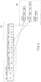
- the nonvolatile memory 28 stores such information as shown in FIG. 5 .
- FIG. 5 is a diagram explaining another process performed in the IC card 2 of FIG. 2 .
- the IC card 2 may receive a command for writing a TLV data object (higher TLV object) having Value that contains a plurality of TLV data objects (lower TLV data objects). In this case, the CPU 25 of the IC card 2 writes such data as shown in FIG. 5 .
- the CPU 25 writes the data values of Value of the lower TLV data objects in the second storage area 28b.
- the CPU 25 further writes Tag and Length of the higher TLV data object in the first storage area 28a.
- the CPU 25 replaces Value of the lower TLV data object with the address specifying the position at which the data value of Value has been written.
- the CPU 25 then writes the lower TLV data object, Value of which has been so replaced, at the position of Value of the higher TLV data object.
- Tag, Length and address of the TLV data object stored in the first storage area 28a have fixed lengths, respectively.
- the number of bytes constituting Tag, the number of bytes constituting Length, and the number of bytes constituting the pointer are stored, as attribute data, in the file held in the nonvolatile memory 28.
- the data showing that Value of the higher TLV data object has lower TLV data objects is also stored, as attribute data, in the nonvolatile memory 28.
- the CPU 25 confirms the attribute data held in the file. The CPU 25 can therefore recognize that Value of the higher TLV data object has lower TLV data objects.
- the CPU 25 examines the attribute data, determining the lengths of Tag, Length and address. That is, the CPU 25 confirms the data length of each lower TLV data object. When the CPU 25 confirms Length of the higher TLV data object, it can recognize how many lower TLV objects are contained in the higher TLV data object.
- the CPU 25 of the IC card 2 in which the nonvolatile memory 28 stores the data shown in FIG. 5 may receive, from the IC card processing apparatus 1, a GET DATA command designating "A5.” In this case, the CPU 25 retrieves TLV data object whose Tag value is "A5".
- the CPU 25 reads Tag 1 from the head of the file. Then, the CPU 25 collates the value of Tag 1 with the value of the designation data. As shown in FIG. 5 , Tag 1 has value "70,” and the designation data has value "A5.” Therefore, the CPU 25 determines that the value of Tag 1 is not equal to that of the designation data.
- the CPU 25 therefore moves the data pointer to the next tag, i.e., Tag 2. That is, the CPU 25 does not read Length 1, on the basis of the length of Length previously recognized.
- the CPU 25 then reads Tag 2.
- the CPU 25 collates the value of Tag 2 with the value of the designation data. As shown in FIG. 5 , Tag 2 has value "88," and the designation data has value "A5.” The CPU 5 therefore determines that the value of Tag 2 is not equal to that of the designation data.
- the CPU 25 moves the data pointer to the next tag, i.e., Tag 3. That is, the CPU 25 does not read Length 1 or Length 2, on the basis of the length of Length or pointer 2, both previously recognized.
- the CPU 25 reads Tag 3.
- the CPU 25 collates the value of Tag 3 with the value of the designation data. As shown in FIG. 5 , Tag 3 has value "50,” and the designation data has value "A5.” The CPU 5 therefore determines that the value of Tag 3 is not equal to that of the designation data.
- the CPU 25 therefore moves the data pointer to the next tag, i.e., Tag 4. That is, the CPU 25 does not read Length 3 or pointer 3, on the basis of the length of Length and the length of the address, both previously recognized.
- the CPU 25 reads Tag 4.
- the CPU 25 collates Tag 4 with the value of the designation data. As shown in FIG. 5 , Tag 5 has value "A5,” and the designation data has value "A5.” The CPU 5 therefore determines that the value of Tag 3 is equal to that of the designation data.
- the CPU 25 reads the value of Length 4 stored at the back Tag 4.
- the CPU 25 also reads the value of pointer 4 stored at the back of Length 4.
- the CPU 25 moves the data pointer on the basis of the value of pointer 4.
- the CPU 25 reads data (Value 4) defined by the number of bytes, indicated by Length 4, from the position the data pointer indicates.
- the CPU 25 generates response data from the value of Value thus read.
- the CPU 25 transmits the response data to the card reader/writer 14 through the communication unit 24.
- this embodiment can be practiced even if Value of the higher TLV data object contains a plurality of lower TLV objects.
- the CPU 25 can shorten the time required for retrieving TLV data objects.
- a portable electronic apparatus and a method of controlling the portable electronic apparatus can be provided, in which processes can be efficiently performed in response to commands.
- the TLV data objects stored in the file may differ in the data length of Length.
- the nonvolatile memory 28 stores such data as shown in FIG. 6 .
- FIG. 6 is a diagram explaining still another process performed in the IC card 2 of FIG. 2 . If the TLV data objects to be written in the file differ in the length of Length, the CPU 25 of the IC card 2 writes such data as shown in FIG. 6 .
- the CPU 25 writes Length and Value of the TLV data object in the second storage area 28b. In this case, Value is written immediately after Length.
- the CPU 25 writes Tag of the TLV data object in the first storage area 28a. Moreover, the CPU 25 writes address for specifying the position where Length and Value of the TLV data object have been written, in first storage area 28a and immediately after Tag.
- Tag and length of address of the TLV data object stored in the first storage area 28a have fixed lengths, respectively.
- the number of bytes constituting Tag and the number of bytes constituting the pointer are stored, as attribute data, in the file held in the nonvolatile memory 28. Further, the data showing that the file hold a TLV data object having an unfixed length is also stored, as attribute data, in the nonvolatile memory 28.
- the CPU 25 confirms the attribute data held in the file. The CPU 25 can therefore recognize that the file holds a TLV data object having an unfixed length. Further, the CPU 25 examines the attribute data, determining the lengths of Tag and address.
- the CPU 25 of the IC card 2 in which the nonvolatile memory 28 stores the data shown in FIG. 6 may receive, from the IC card processing apparatus 1, a GET DATA command designating "A5.” In this case, the CPU 25 retrieves TLV data object whose Tag value is "A5.”
- the CPU 25 reads Tag 1 from the head of the file. Then, the CPU 25 collates the value of Tag 1 with the value of the designation data. As shown in FIG. 6 , Tag 1 has value "88," and the designation data has value "A5.” Therefore, the CPU 25 determines that the value of Tag 1 is not equal to that of the designation data.
- the CPU 25 therefore moves the data pointer to the next tag, i.e., Tag 2. That is, the CPU 25 does not read Length 1, on the basis of the length of Length previously recognized.
- the CPU 25 then reads Tag 2.
- the CPU 25 collates the value of Tag 2 with the value of the designation data. As shown in FIG. 6 , Tag 2 has value "50,” and the designation data has value "A5.” The CPU 5 therefore determines that the value of Tag 2 is not equal to that of the designation data.
- the CPU 25 moves the data pointer to the next tag, i.e., Tag 3. That is, the CPU 25 does not read pointer 2 stored immediately after Tag 2, on the basis of the length of the address, which has been previously recognized.
- the CPU 25 reads Tag 3.
- the CPU 25 collates the value of Tag 3 with the value of the designation data. As shown in FIG. 6 , Tag 3 has value "A5,” and the designation data has value "A5.” The CPU 5 therefore determines that the value of Tag 3 is equal to that of the designation data.
- the CPU 25 reads the value of pointer 3 stored at the back Tag 3.
- the CPU 25 moves the data pointer on the basis of the value of pointer 3.
- the CPU 25 reads data (Value 3) defined by the number of bytes, indicated by Length 3, from the position the data pointer indicates.
- the CPU 25 generates response data from the value of Value thus read.
- the CPU 25 transmits the response data to the card reader/writer 14 through the communication unit 24.
- the CPU 25 of the IC card 2 stores Tag and the address in the first storage area 28a, and stores Length and Value in the second storage area 28b.
- Tag and the address, both stored in the first storage area 28a, can therefore have prescribed lengths, respectively.
- the CPU 25 can therefore automatically determine the position at which Tag is stored in the first storage area 28a. That is, the CPU 25 can easily specify the position where Tag is stored, in order to retrieve Tag in accordance with the data the command designates.
- the CPU 25 can shorten the time required for retrieving TLV data objects.
- a portable electronic apparatus and a method of controlling the portable electronic apparatus can be provided, in which processes can be efficiently performed in response to commands.
- Tag of any TLV data object stored in the file may not have a fixed length.
- the nonvolatile memory 28 stores such data as shown in FIG. 7 .
- FIG. 7 is a diagram explaining another process performed in the IC card 2 of FIG. 2 .
- the CPU 25 of the IC card 2 writes such data as shown in FIG. 7 .
- the CPU 25 If the IC card 2 receives a command for writing a TLV data object, the CPU 25 writes Length and Value of the TLV data object in the second storage area 28b. In this case, the CPU 25 writes Value immediately after Value.
- the CPU 25 writes Tag of the TLV data object in the first storage area 28a. Moreover, the CPU 25 writes address for specifying the position where Length and Value of the TLV data object have been written, in first storage area 28a and immediately after Tag.
- the CPU 25 adjusts the length of Tag to be written in the first storage area 28a, to the length of the longest Tag. Assume that three TLV data objects have Tag "9F 38," Tag “9F 27” and Tag “A5,” respectively, as shown in FIG. 7 . Then, the CPU 25 sets the length of Tag to two bytes, in order to write these TLV data objects in first storage area 28a.
- the CPU 25 performs a write process, writing Tag "A5" of the TLV data object having a 2-byte Tag length, as 5 (NULL)." That is, the CPU 25 first adds a blank (NULL) to Tag shorter than a prescribed length, and then writes the tag. The CPU 25 thus adjusts the length of Tag to be written in the first storage area 28a, to the prescribed length.
- the CPU 25 stores the lengths of Tag and pointer, as attribute data, in the file held in the nonvolatile memory 28.
- the CPU 25 confirms the attribute data held in the file.
- the CPU 25 can therefore recognize the lengths of Tag and address, both held in the file.
- the CPU 25 of the IC card 2 in which the nonvolatile memory 28 stores the data shown in FIG. 7 may receive, from the IC card processing apparatus 1, a GET DATA command designating "A5.” In this case, the CPU 25 retrieves TLV data object whose Tag value is "A5.”
- the CPU 25 reads Tag 1 from the head the file. Then, the CPU 25 collates the value of Tag 1 with the value of the designation data. As shown in FIG. 7 , Tag 1 has value "9F 38," and the designation data has value "A5.” Therefore, the CPU 25 determines that the value of Tag 1 is not equal to that of the designation data.
- the CPU 25 therefore moves the data pointer to the next tag, i.e., Tag 2. That is, the CPU 25 does not read pointer 1 existing immediately after Tag 1, on the basis of the length of the address recognized.
- the CPU 25 then reads Tag 2.
- the CPU 25 collates the value of Tag 2 with the value of the designation data. As shown in FIG. 7 , Tag 2 has value "9F 27," and the designation data has value "A5.” The CPU 5 therefore determines that the value of Tag 2 is not equal to that of the designation data.
- the CPU 25 moves the data pointer to the next tag, i.e., Tag 3. That is, the CPU 25 does not read pointer 2 stored immediately after Tag 2, on the basis of the length of the address, which has been previously recognized.
- the CPU 25 reads Tag 3.
- the CPU 25 collates the value of Tag 3 with the value of the designation data. As shown in FIG. 7 , Tag 3 has value "A5,” and the designation data has value "A5.” The CPU 5 therefore determines that the value of Tag 3 is equal to that of the designation data.
- the CPU 25 reads the value of pointer 3 stored at the back Tag 3.
- the CPU 25 moves the data pointer on the basis of the value of pointer 3.
- the CPU 25 reads Length 3 from the position the data pointer indicates.
- the CPU 25 reads data (Value 3) defined by the number of bytes, indicated by Length 3.
- the CPU 25 generates response data from the value of Value thus read.
- the CPU 25 transmits the response data to the card reader/writer 14 through the communication unit 24.
- the CPU 25 of the IC card 2 performs a write process, adjusting the length of Tag to be written in the first storage area 28a, to the length of the longest Tag.
- Tag can therefore written in units of a specific number of bytes, even if the TLV data objects to be written in the first storage area 28a differ in the length of Tag.
- the CPU 25 can therefore automatically determine the position at which Tag is stored in the first storage area 28a. That is, the CPU 25 can easily specify the position where Tag is stored, in order to retrieve Tag in accordance with the data the command designates.
- the CPU 25 can shorten the time required for retrieving TLV data objects.
- a portable electronic apparatus and a method of controlling the portable electronic apparatus can be provided, in which processes can be efficiently performed in response to commands.
- TLV data objects are is held in the file stored in the nonvolatile memory 28. Then, Tag of one TLV data object is stored immediately after Value of the preceding TLV data object. This makes the problem that any data to be updated cannot be stored if it is longer than Value already stored.
- the storage area for holding Tag and Length is spaced from the storage area for holding Value. Value can therefore be updated to longer data.
- FIG. 8 is a diagram explaining how data is updated in the IC card of FIG. 2 .
- the IC card 2 may receive an update command for updating a designated TLV data object of a file stored in the nonvolatile memory 28.
- the CPU 25 of the IC card 2 first specifies the designated file. More precisely, the CPU 25 retrieves, from the nonvolatile memory 28, the TLV data object having Tag identical to the designation data contained in the update command.
- the CPU 25 retrieves Tag of the value equal to "50" from the first storage area 28a. In this case, the CPU 25 retrieves Tag identical to the designation data, performing the process explained with reference to FIG. 3 . The CPU 25 can therefore determine that the designation data is identical to Tag 2 shown in FIG. 8 .
- the CPU 25 reads Length 2 stored at the back of Tag 2. The CPU 25 then compares the value of Length of the TLV data object to update, with the value of Length 2. If the value of Length of the TLV data object to update is greater than the value of Length 2, the CPU 25 deletes Value 2 in the second storage area 28b.
- the CPU 25 reads the value of pointer 2 stored right after Length 2. On the basis of the value of pointer 2, the CPU 25 moves the data pointer. The CPU 25 then deletes data (i.e., Value 2) composed of a number of bytes, equivalent to Length 2, from the position the data pointer indicates.
- the CPU 25 further moves the data pointer to another address in the second storage area 28b.
- the CPU 25 writes Value of the TLV data object to update (i.e., Value 2') from the position of the data pointer.
- the CPU 25 then rewrites the value "04" of Length 2 stored in the first storage area 28a to the value "05" of Length 2' of the TLV data object to update. Further, the CPU 25 rewrites the value of pointer 2 stored in the first storage area 28a, to the value of pointer 2' indicating the position at which Value 2' is stored.
- the CPU 25 of the IC card 2 discards the storage area in which Value is stored. Moreover, the CPU 25 writes new Value in another part of the second storage area 28b. In accordance with new Value so written, the CPU 25 rewrites Length and pointer, both stored in the first storage area 28a.
- Value already stored can be updated to Value of a longer data length.
- the restriction placed on the updating of TLV data objects can thereby eliminated.
Landscapes
- Engineering & Computer Science (AREA)
- Theoretical Computer Science (AREA)
- Physics & Mathematics (AREA)
- General Engineering & Computer Science (AREA)
- General Physics & Mathematics (AREA)
- Information Retrieval, Db Structures And Fs Structures Therefor (AREA)
- Selective Calling Equipment (AREA)
- Credit Cards Or The Like (AREA)
Claims (7)
- Tragbares elektronisches Gerät (2), das eingerichtet ist, basierend auf einer Befehlseingabe von einem externen Gerät (10) einen Prozess auszuführen und eine Mehrzahl von Tag-Length-Value (Typ-Länge-Wert)- bzw. TLV-Datenobjekten abzuspeichern, wobei das Gerät gekennzeichnet ist, durch:eine Speichereinheit (28), die eingerichtet ist, zumindest eine Datei zu speichern, mit einem ersten Speicherbereich (28a) und einem zweiten Speicherbereich (28b), wobei:der erste Speicherbereich (28a) eingerichtet ist, für jedes TLV-Datenobjekt eine Datenklasse und eine Adresse mit fester Länge, die die Position von Datenzeichen des entsprechenden TLV-Datenobjekts repräsentiert, speichert, wobei die Datenklasse und die Adresse mit fester Länge zugeordnet zueinander gespeichert werden, undder zweite Speicherbereich (28b) eingerichtet ist, die Datenzeichen der TLV-Datenobjekte zu speichern,wobei die Adresse mit fester Länge ein Versatzwert zwischen der Position, an der die Adresse mit fester Länge geschrieben ist, und der Position, an der die Datenzeichen des Wertes des TLV-Datenobjekts in den zweiten Speicherbereich (28b) geschrieben sind, ist, oderwobei die Adresse mit fester Länge ein Versatzwert zwischen dem Kopf der mindestens einen Datei, die eine Mehrzahl von miteinander gekoppelten TLV-Datenobjekten enthält, und der Position, an der die Datenzeichen des Wertes des TLV-Datenobjekts in den zweiten Speicherbereich (28b) geschrieben sind, ist; undeine Sende-/Empfangseinheit (24), die eingerichtet ist, Daten zu der externen Vorrichtung (10) zu senden und von dieser zu empfangen; undeine Steuereinheit (25), die eingerichtet ist, dass dann, falls ein Lesebefehl zum Lesen eines TLV-Objekts von der Sende-/Empfangseinheit (24) empfangen wird, die Steuereinheit (25) aus dem ersten Speicherbereich (28a) die Datenklasse, die mit in dem Lesebefehl enthaltenen Bezeichnungsdaten identisch ist, abruft und die in dem zweiten Speicherbereich (28b) gespeicherten Datenzeichen basierend auf der der abgerufenen Datenklasse zugeordneten Adresse mit fester Länge liest.
- Tragbares elektronisches Gerät (2) nach Anspruch 1,
dadurch gekennzeichnet, dass die Speichereinheit (28) eingerichtet ist, eine Datenlänge zu speichern, die die Länge des in dem zweiten Speicherbereich (28b) gespeicherten Datenzeichens zu der in dem ersten Speicherbereich (28a) gespeicherten Datenklasse zugeordnet repräsentiert. - Tragbares elektronisches Gerät (2) nach Anspruch 1,
dadurch gekennzeichnet, dass die Speichereinheit (28) eingerichtet ist, eine Datenlänge zu speichern, die die Länge des in dem zweiten Speicherbereich (28b) zu speichernden Datenzeichens zu dem in dem zweiten Speicherbereich (28b) gespeicherten Datenzeichen zugeordnet repräsentiert. - Tragbares elektronisches Gerät (2) nach Anspruch 2,
dadurch gekennzeichnet, dass die Steuereinheit (25) eingerichtet ist, das Datenzeichen des zu aktualisierenden TLV-Datenobjekts zu speichern und die Adresse und die Datenlänge, die beide der in dem ersten Speicherbereich (28a) gespeicherten Datenklasse gemäß dem in dem zweiten Speicherbereich (28b) gespeicherten Datenzeichen zugeordnet sind, zu aktualisieren, wenn die Sende-/Empfangseinheit einen Befehl zum Aktualisieren des TLV-Datenobjekts empfängt. - Tragbares elektronisches Gerät (2) nach Anspruch 1,
dadurch gekennzeichnet, dass die Speichereinheit (28) eingerichtet ist, die Datenklasse in dem ersten Speicherbereich (28a) zu speichern, wobei die Datenlänge der Datenklasse an die Datenlänge des längsten TLV-Datenobjekts anpasst wird. - Tragbares elektronisches Gerät (2) nach Anspruch 1,
ferner gekennzeichnet, durch:ein IC-Modul (22), das die Speichereinheit (28) enthält; undeinen Hauptkörper (21), der das IC-Modul enthält. - Verfahren zum Steuern eines tragbaren elektronischen Gerätes (2) zum Ausführen eines Prozesses basierend auf einer Befehlseingabe von einem externen Gerät (10) und zum Speichern einer Mehrzahl von Tag-Length-Value- bzw. TLV-Datenobjekten, wobei das Gerät eine Speichereinheit (29) umfasst, die eingerichtet ist, zumindest eine Datei zu speichern, mit einem ersten Bereich (28a) und einem zweiten Bereich (28b), wobei das Verfahren gekennzeichnet ist, durch:Speichern einer Datenklasse und einer Adresse mit fester Länge, die die Position von Datenzeichen des entsprechenden TLV-Datenobjekts repräsentiert, in dem ersten Speicherbereich (28a) für jedes TLV-Datenobjekt, wobei die Datenklasse und die Adresse mit fester Länge zueinander zugeordnet gespeichert werden,Speichern der Datenzeichen der TLV-Datenobjekte in dem zweiten Speicherbereich (28b),wobei die Adresse mit fester Länge ein Versatzwert zwischen der Position, an der die Adresse mit fester Länge geschrieben ist, und der Position, an der die Datenzeichen des Wertes des TLV-Datenobjekts in den zweiten Speicherbereich (28b) geschrieben sind, ist, oderwobei die Adresse mit fester Länge ein Versatzwert zwischen dem Kopf der zumindest einen Datei, die eine Mehrzahl von miteinander gekoppelten TLV-Datenobjekten enthält, und der Position, an der die Datenzeichen des Wertes des TLV-Datenobjekts in den zweiten Speicherbereich (28b) geschrieben sind, ist,falls ein Lesebefehl zum Lesen eines TLV-Objekts empfangen wird:Abrufen der Datenklasse, die mit den in dem Lesebefehl enthaltenen Bezeichnungsdaten identisch ist, aus dem ersten Speicherbereich (28a), undLesen der in dem zweiten Speicherbereich (28b) gespeicherten Datenzeichen basierend auf der der abgerufenen Datenklasse zugeordneten Adresse mit fester Länge.
Applications Claiming Priority (1)
| Application Number | Priority Date | Filing Date | Title |
|---|---|---|---|
| JP2010063324A JP5150672B2 (ja) | 2010-03-18 | 2010-03-18 | 携帯可能電子装置、及び携帯可能電子装置の制御方法 |
Publications (3)
| Publication Number | Publication Date |
|---|---|
| EP2367115A1 EP2367115A1 (de) | 2011-09-21 |
| EP2367115B1 EP2367115B1 (de) | 2019-05-22 |
| EP2367115B9 true EP2367115B9 (de) | 2019-11-06 |
Family
ID=44265690
Family Applications (1)
| Application Number | Title | Priority Date | Filing Date |
|---|---|---|---|
| EP11155881.3A Active EP2367115B9 (de) | 2010-03-18 | 2011-02-24 | Tragbares elektronisches Gerät und Verfahren zur Steuerung eines tragbaren elektronischen Geräts |
Country Status (4)
| Country | Link |
|---|---|
| US (1) | US8977824B2 (de) |
| EP (1) | EP2367115B9 (de) |
| JP (1) | JP5150672B2 (de) |
| SG (1) | SG174682A1 (de) |
Families Citing this family (5)
| Publication number | Priority date | Publication date | Assignee | Title |
|---|---|---|---|---|
| EP4234254A3 (de) | 2013-07-31 | 2023-09-13 | Hewlett-Packard Development Company, L.P. | Schutz von daten im speicher eines verbrauchsprodukts |
| DE102015210719A1 (de) * | 2015-06-11 | 2016-12-15 | Bundesdruckerei Gmbh | Verfahren zum Aktualisieren von Personalisierungsdaten |
| JP6750450B2 (ja) * | 2016-10-20 | 2020-09-02 | 大日本印刷株式会社 | 電子情報記憶媒体、データ送信方法、icカード及びデータ送信プログラム |
| CN107835184A (zh) * | 2017-11-20 | 2018-03-23 | 北京东土军悦科技有限公司 | Tlv数据段处理方法、装置、电子设备及存储介质 |
| CN112073660B (zh) * | 2020-09-15 | 2023-03-10 | 深圳Tcl数字技术有限公司 | Tlv数据生成方法、读取方法、智能设备及存储介质 |
Family Cites Families (11)
| Publication number | Priority date | Publication date | Assignee | Title |
|---|---|---|---|---|
| JPH0648506B2 (ja) * | 1986-06-23 | 1994-06-22 | 松下電工株式会社 | 情報記録装置 |
| JPH09231113A (ja) * | 1995-12-22 | 1997-09-05 | Dainippon Printing Co Ltd | Icカード |
| JP3877890B2 (ja) * | 1997-12-22 | 2007-02-07 | 株式会社日立製作所 | Icカードおよび表示装置 |
| US6484946B2 (en) * | 1997-12-22 | 2002-11-26 | Hitachi, Ltd. | IC card information display device and IC card for use therewith |
| JP3543649B2 (ja) * | 1998-10-27 | 2004-07-14 | セイコーエプソン株式会社 | データ転送制御装置及び電子機器 |
| JP4342629B2 (ja) * | 1999-03-24 | 2009-10-14 | 株式会社東芝 | 携帯可能電子装置とファイル制御情報の記憶方法とファイル制御情報の検索方法 |
| JP4828809B2 (ja) | 2003-12-10 | 2011-11-30 | 株式会社東芝 | Icカードおよびicカードにおける処理方法 |
| US7873663B2 (en) * | 2004-01-13 | 2011-01-18 | International Business Machines Corporation | Methods and apparatus for converting a representation of XML and other markup language data to a data structure format |
| JP4667459B2 (ja) * | 2005-07-05 | 2011-04-13 | パナソニック株式会社 | 読出しデータ長の指定方法 |
| JP4891587B2 (ja) * | 2005-09-30 | 2012-03-07 | 株式会社東芝 | 携帯可能電子装置、icカードおよびicモジュール |
| WO2008078217A2 (en) | 2006-12-22 | 2008-07-03 | Nxp B.V. | A method for storing data as well as a transponder, a read/write-device, a computer readable medium including a program element and such a program element adapted to perform this method |
-
2010
- 2010-03-18 JP JP2010063324A patent/JP5150672B2/ja not_active Expired - Fee Related
-
2011
- 2011-02-24 EP EP11155881.3A patent/EP2367115B9/de active Active
- 2011-02-24 US US13/033,640 patent/US8977824B2/en not_active Expired - Fee Related
- 2011-02-28 SG SG2011014610A patent/SG174682A1/en unknown
Also Published As
| Publication number | Publication date |
|---|---|
| JP5150672B2 (ja) | 2013-02-20 |
| EP2367115B1 (de) | 2019-05-22 |
| US20110231617A1 (en) | 2011-09-22 |
| SG174682A1 (en) | 2011-10-28 |
| JP2011197960A (ja) | 2011-10-06 |
| US8977824B2 (en) | 2015-03-10 |
| EP2367115A1 (de) | 2011-09-21 |
Similar Documents
| Publication | Publication Date | Title |
|---|---|---|
| US8931705B2 (en) | IC card, mobile electronic device and data processing method in IC card | |
| EP2367115B1 (de) | Tragbares elektronisches Gerät und Verfahren zur Steuerung eines tragbaren elektronischen Geräts | |
| US9183400B2 (en) | IC card and IC card control method | |
| EP2278501B1 (de) | Chipkarte für eine tragbare elektronische Vorrichtung | |
| US20090012975A1 (en) | Portable electronic device and file management method for use in portable electronic device | |
| JP5624685B2 (ja) | Icカード及びicカード処理システム | |
| US20100235393A1 (en) | Portable electronic device and access control method in portable electronic device | |
| US20120234926A1 (en) | Portable electronic apparatus | |
| JP4590201B2 (ja) | データキャリア及びデータキャリアのプログラム | |
| JP5433358B2 (ja) | 携帯可能電子装置 | |
| JP7005934B2 (ja) | 電子情報記憶媒体、icカード、データ送信方法、データ書き込み方法、データ送信プログラム及びデータ書き込みプログラム | |
| EP2782019A2 (de) | Chipkarte und tragbare elektronische Vorrichtung | |
| JP6984328B2 (ja) | 電子情報記憶媒体、icカード、外部機器、データ書き込み方法及びデータ書き込みプログラム | |
| JP2012133656A (ja) | 携帯可能電子装置及びicカード | |
| JP4836707B2 (ja) | 携帯可能電子装置およびicカード | |
| KR101455539B1 (ko) | Ic 카드 및 ic 카드 제어 방법 | |
| JP4738249B2 (ja) | 携帯可能電子装置、icカードおよびicモジュール | |
| JP2009032249A (ja) | 携帯可能電子装置、携帯可能電子装置のファイル管理方法及びicカード | |
| JP2014006631A (ja) | Icカード、および、携帯可能電子装置 | |
| JP2009176034A (ja) | 携帯可能電子装置、及び、データ管理方法 | |
| JP2021099632A (ja) | Icカード及びicカードの制御プログラム | |
| JP2018067187A (ja) | 電子情報記憶媒体、データ送信方法、icカード及びデータ送信プログラム | |
| JP2000148944A (ja) | Icカード |
Legal Events
| Date | Code | Title | Description |
|---|---|---|---|
| PUAI | Public reference made under article 153(3) epc to a published international application that has entered the european phase |
Free format text: ORIGINAL CODE: 0009012 |
|
| 17P | Request for examination filed |
Effective date: 20110224 |
|
| AK | Designated contracting states |
Kind code of ref document: A1 Designated state(s): AL AT BE BG CH CY CZ DE DK EE ES FI FR GB GR HR HU IE IS IT LI LT LU LV MC MK MT NL NO PL PT RO RS SE SI SK SM TR |
|
| AX | Request for extension of the european patent |
Extension state: BA ME |
|
| 17Q | First examination report despatched |
Effective date: 20150526 |
|
| REG | Reference to a national code |
Ref country code: DE Ref legal event code: R079 Ref document number: 602011059122 Country of ref document: DE Free format text: PREVIOUS MAIN CLASS: G06F0012040000 Ipc: H04L0012751000 |
|
| GRAP | Despatch of communication of intention to grant a patent |
Free format text: ORIGINAL CODE: EPIDOSNIGR1 |
|
| STAA | Information on the status of an ep patent application or granted ep patent |
Free format text: STATUS: GRANT OF PATENT IS INTENDED |
|
| RIC1 | Information provided on ipc code assigned before grant |
Ipc: G06F 17/21 20060101ALI20181116BHEP Ipc: H04L 12/751 20130101AFI20181116BHEP |
|
| INTG | Intention to grant announced |
Effective date: 20181205 |
|
| RIC1 | Information provided on ipc code assigned before grant |
Ipc: H04L 12/751 20130101AFI20181116BHEP Ipc: G06F 17/21 20060101ALI20181116BHEP |
|
| GRAS | Grant fee paid |
Free format text: ORIGINAL CODE: EPIDOSNIGR3 |
|
| GRAA | (expected) grant |
Free format text: ORIGINAL CODE: 0009210 |
|
| STAA | Information on the status of an ep patent application or granted ep patent |
Free format text: STATUS: THE PATENT HAS BEEN GRANTED |
|
| AK | Designated contracting states |
Kind code of ref document: B1 Designated state(s): AL AT BE BG CH CY CZ DE DK EE ES FI FR GB GR HR HU IE IS IT LI LT LU LV MC MK MT NL NO PL PT RO RS SE SI SK SM TR |
|
| REG | Reference to a national code |
Ref country code: GB Ref legal event code: FG4D |
|
| RIN1 | Information on inventor provided before grant (corrected) |
Inventor name: SEKIYA, SATOSHI |
|
| REG | Reference to a national code |
Ref country code: CH Ref legal event code: EP |
|
| REG | Reference to a national code |
Ref country code: IE Ref legal event code: FG4D |
|
| REG | Reference to a national code |
Ref country code: DE Ref legal event code: R096 Ref document number: 602011059122 Country of ref document: DE |
|
| REG | Reference to a national code |
Ref country code: AT Ref legal event code: REF Ref document number: 1137431 Country of ref document: AT Kind code of ref document: T Effective date: 20190615 |
|
| GRAT | Correction requested after decision to grant or after decision to maintain patent in amended form |
Free format text: ORIGINAL CODE: EPIDOSNCDEC |
|
| REG | Reference to a national code |
Ref country code: NL Ref legal event code: MP Effective date: 20190522 |
|
| REG | Reference to a national code |
Ref country code: LT Ref legal event code: MG4D |
|
| REG | Reference to a national code |
Ref country code: CH Ref legal event code: PK Free format text: BERICHTIGUNG B9 |
|
| PG25 | Lapsed in a contracting state [announced via postgrant information from national office to epo] |
Ref country code: FI Free format text: LAPSE BECAUSE OF FAILURE TO SUBMIT A TRANSLATION OF THE DESCRIPTION OR TO PAY THE FEE WITHIN THE PRESCRIBED TIME-LIMIT Effective date: 20190522 Ref country code: LT Free format text: LAPSE BECAUSE OF FAILURE TO SUBMIT A TRANSLATION OF THE DESCRIPTION OR TO PAY THE FEE WITHIN THE PRESCRIBED TIME-LIMIT Effective date: 20190522 Ref country code: HR Free format text: LAPSE BECAUSE OF FAILURE TO SUBMIT A TRANSLATION OF THE DESCRIPTION OR TO PAY THE FEE WITHIN THE PRESCRIBED TIME-LIMIT Effective date: 20190522 Ref country code: PT Free format text: LAPSE BECAUSE OF FAILURE TO SUBMIT A TRANSLATION OF THE DESCRIPTION OR TO PAY THE FEE WITHIN THE PRESCRIBED TIME-LIMIT Effective date: 20190922 Ref country code: SE Free format text: LAPSE BECAUSE OF FAILURE TO SUBMIT A TRANSLATION OF THE DESCRIPTION OR TO PAY THE FEE WITHIN THE PRESCRIBED TIME-LIMIT Effective date: 20190522 Ref country code: NO Free format text: LAPSE BECAUSE OF FAILURE TO SUBMIT A TRANSLATION OF THE DESCRIPTION OR TO PAY THE FEE WITHIN THE PRESCRIBED TIME-LIMIT Effective date: 20190822 Ref country code: AL Free format text: LAPSE BECAUSE OF FAILURE TO SUBMIT A TRANSLATION OF THE DESCRIPTION OR TO PAY THE FEE WITHIN THE PRESCRIBED TIME-LIMIT Effective date: 20190522 Ref country code: ES Free format text: LAPSE BECAUSE OF FAILURE TO SUBMIT A TRANSLATION OF THE DESCRIPTION OR TO PAY THE FEE WITHIN THE PRESCRIBED TIME-LIMIT Effective date: 20190522 Ref country code: NL Free format text: LAPSE BECAUSE OF FAILURE TO SUBMIT A TRANSLATION OF THE DESCRIPTION OR TO PAY THE FEE WITHIN THE PRESCRIBED TIME-LIMIT Effective date: 20190522 |
|
| PG25 | Lapsed in a contracting state [announced via postgrant information from national office to epo] |
Ref country code: BG Free format text: LAPSE BECAUSE OF FAILURE TO SUBMIT A TRANSLATION OF THE DESCRIPTION OR TO PAY THE FEE WITHIN THE PRESCRIBED TIME-LIMIT Effective date: 20190822 Ref country code: RS Free format text: LAPSE BECAUSE OF FAILURE TO SUBMIT A TRANSLATION OF THE DESCRIPTION OR TO PAY THE FEE WITHIN THE PRESCRIBED TIME-LIMIT Effective date: 20190522 Ref country code: LV Free format text: LAPSE BECAUSE OF FAILURE TO SUBMIT A TRANSLATION OF THE DESCRIPTION OR TO PAY THE FEE WITHIN THE PRESCRIBED TIME-LIMIT Effective date: 20190522 Ref country code: GR Free format text: LAPSE BECAUSE OF FAILURE TO SUBMIT A TRANSLATION OF THE DESCRIPTION OR TO PAY THE FEE WITHIN THE PRESCRIBED TIME-LIMIT Effective date: 20190823 |
|
| REG | Reference to a national code |
Ref country code: AT Ref legal event code: MK05 Ref document number: 1137431 Country of ref document: AT Kind code of ref document: T Effective date: 20190522 |
|
| PG25 | Lapsed in a contracting state [announced via postgrant information from national office to epo] |
Ref country code: SK Free format text: LAPSE BECAUSE OF FAILURE TO SUBMIT A TRANSLATION OF THE DESCRIPTION OR TO PAY THE FEE WITHIN THE PRESCRIBED TIME-LIMIT Effective date: 20190522 Ref country code: RO Free format text: LAPSE BECAUSE OF FAILURE TO SUBMIT A TRANSLATION OF THE DESCRIPTION OR TO PAY THE FEE WITHIN THE PRESCRIBED TIME-LIMIT Effective date: 20190522 Ref country code: EE Free format text: LAPSE BECAUSE OF FAILURE TO SUBMIT A TRANSLATION OF THE DESCRIPTION OR TO PAY THE FEE WITHIN THE PRESCRIBED TIME-LIMIT Effective date: 20190522 Ref country code: DK Free format text: LAPSE BECAUSE OF FAILURE TO SUBMIT A TRANSLATION OF THE DESCRIPTION OR TO PAY THE FEE WITHIN THE PRESCRIBED TIME-LIMIT Effective date: 20190522 Ref country code: AT Free format text: LAPSE BECAUSE OF FAILURE TO SUBMIT A TRANSLATION OF THE DESCRIPTION OR TO PAY THE FEE WITHIN THE PRESCRIBED TIME-LIMIT Effective date: 20190522 Ref country code: CZ Free format text: LAPSE BECAUSE OF FAILURE TO SUBMIT A TRANSLATION OF THE DESCRIPTION OR TO PAY THE FEE WITHIN THE PRESCRIBED TIME-LIMIT Effective date: 20190522 |
|
| REG | Reference to a national code |
Ref country code: DE Ref legal event code: R097 Ref document number: 602011059122 Country of ref document: DE |
|
| PG25 | Lapsed in a contracting state [announced via postgrant information from national office to epo] |
Ref country code: SM Free format text: LAPSE BECAUSE OF FAILURE TO SUBMIT A TRANSLATION OF THE DESCRIPTION OR TO PAY THE FEE WITHIN THE PRESCRIBED TIME-LIMIT Effective date: 20190522 Ref country code: IT Free format text: LAPSE BECAUSE OF FAILURE TO SUBMIT A TRANSLATION OF THE DESCRIPTION OR TO PAY THE FEE WITHIN THE PRESCRIBED TIME-LIMIT Effective date: 20190522 |
|
| PLBE | No opposition filed within time limit |
Free format text: ORIGINAL CODE: 0009261 |
|
| STAA | Information on the status of an ep patent application or granted ep patent |
Free format text: STATUS: NO OPPOSITION FILED WITHIN TIME LIMIT |
|
| PG25 | Lapsed in a contracting state [announced via postgrant information from national office to epo] |
Ref country code: TR Free format text: LAPSE BECAUSE OF FAILURE TO SUBMIT A TRANSLATION OF THE DESCRIPTION OR TO PAY THE FEE WITHIN THE PRESCRIBED TIME-LIMIT Effective date: 20190522 |
|
| 26N | No opposition filed |
Effective date: 20200225 |
|
| PG25 | Lapsed in a contracting state [announced via postgrant information from national office to epo] |
Ref country code: PL Free format text: LAPSE BECAUSE OF FAILURE TO SUBMIT A TRANSLATION OF THE DESCRIPTION OR TO PAY THE FEE WITHIN THE PRESCRIBED TIME-LIMIT Effective date: 20190522 |
|
| PG25 | Lapsed in a contracting state [announced via postgrant information from national office to epo] |
Ref country code: SI Free format text: LAPSE BECAUSE OF FAILURE TO SUBMIT A TRANSLATION OF THE DESCRIPTION OR TO PAY THE FEE WITHIN THE PRESCRIBED TIME-LIMIT Effective date: 20190522 |
|
| PGFP | Annual fee paid to national office [announced via postgrant information from national office to epo] |
Ref country code: FR Payment date: 20200113 Year of fee payment: 10 |
|
| REG | Reference to a national code |
Ref country code: DE Ref legal event code: R119 Ref document number: 602011059122 Country of ref document: DE |
|
| REG | Reference to a national code |
Ref country code: CH Ref legal event code: PL |
|
| GBPC | Gb: european patent ceased through non-payment of renewal fee |
Effective date: 20200224 |
|
| REG | Reference to a national code |
Ref country code: BE Ref legal event code: MM Effective date: 20200229 |
|
| PG25 | Lapsed in a contracting state [announced via postgrant information from national office to epo] |
Ref country code: MC Free format text: LAPSE BECAUSE OF FAILURE TO SUBMIT A TRANSLATION OF THE DESCRIPTION OR TO PAY THE FEE WITHIN THE PRESCRIBED TIME-LIMIT Effective date: 20190522 Ref country code: LU Free format text: LAPSE BECAUSE OF NON-PAYMENT OF DUE FEES Effective date: 20200224 |
|
| PG25 | Lapsed in a contracting state [announced via postgrant information from national office to epo] |
Ref country code: LI Free format text: LAPSE BECAUSE OF NON-PAYMENT OF DUE FEES Effective date: 20200229 Ref country code: CH Free format text: LAPSE BECAUSE OF NON-PAYMENT OF DUE FEES Effective date: 20200229 |
|
| PG25 | Lapsed in a contracting state [announced via postgrant information from national office to epo] |
Ref country code: GB Free format text: LAPSE BECAUSE OF NON-PAYMENT OF DUE FEES Effective date: 20200224 Ref country code: DE Free format text: LAPSE BECAUSE OF NON-PAYMENT OF DUE FEES Effective date: 20200901 Ref country code: IE Free format text: LAPSE BECAUSE OF NON-PAYMENT OF DUE FEES Effective date: 20200224 |
|
| PG25 | Lapsed in a contracting state [announced via postgrant information from national office to epo] |
Ref country code: BE Free format text: LAPSE BECAUSE OF NON-PAYMENT OF DUE FEES Effective date: 20200229 |
|
| PG25 | Lapsed in a contracting state [announced via postgrant information from national office to epo] |
Ref country code: FR Free format text: LAPSE BECAUSE OF NON-PAYMENT OF DUE FEES Effective date: 20210228 |
|
| PG25 | Lapsed in a contracting state [announced via postgrant information from national office to epo] |
Ref country code: MT Free format text: LAPSE BECAUSE OF FAILURE TO SUBMIT A TRANSLATION OF THE DESCRIPTION OR TO PAY THE FEE WITHIN THE PRESCRIBED TIME-LIMIT Effective date: 20190522 Ref country code: CY Free format text: LAPSE BECAUSE OF FAILURE TO SUBMIT A TRANSLATION OF THE DESCRIPTION OR TO PAY THE FEE WITHIN THE PRESCRIBED TIME-LIMIT Effective date: 20190522 |
|
| PG25 | Lapsed in a contracting state [announced via postgrant information from national office to epo] |
Ref country code: MK Free format text: LAPSE BECAUSE OF FAILURE TO SUBMIT A TRANSLATION OF THE DESCRIPTION OR TO PAY THE FEE WITHIN THE PRESCRIBED TIME-LIMIT Effective date: 20190522 Ref country code: IS Free format text: LAPSE BECAUSE OF FAILURE TO SUBMIT A TRANSLATION OF THE DESCRIPTION OR TO PAY THE FEE WITHIN THE PRESCRIBED TIME-LIMIT Effective date: 20190922 |