EP2365632A2 - Konfigurationsverfahren und FPGA-Schaltung - Google Patents
Konfigurationsverfahren und FPGA-Schaltung Download PDFInfo
- Publication number
- EP2365632A2 EP2365632A2 EP11157593A EP11157593A EP2365632A2 EP 2365632 A2 EP2365632 A2 EP 2365632A2 EP 11157593 A EP11157593 A EP 11157593A EP 11157593 A EP11157593 A EP 11157593A EP 2365632 A2 EP2365632 A2 EP 2365632A2
- Authority
- EP
- European Patent Office
- Prior art keywords
- configuration
- circuit
- fpga
- fpga circuit
- data
- Prior art date
- Legal status (The legal status is an assumption and is not a legal conclusion. Google has not performed a legal analysis and makes no representation as to the accuracy of the status listed.)
- Withdrawn
Links
Images


Classifications
-
- H—ELECTRICITY
- H03—ELECTRONIC CIRCUITRY
- H03K—PULSE TECHNIQUE
- H03K19/00—Logic circuits, i.e. having at least two inputs acting on one output; Inverting circuits
-
- H—ELECTRICITY
- H03—ELECTRONIC CIRCUITRY
- H03K—PULSE TECHNIQUE
- H03K19/00—Logic circuits, i.e. having at least two inputs acting on one output; Inverting circuits
- H03K19/02—Logic circuits, i.e. having at least two inputs acting on one output; Inverting circuits using specified components
- H03K19/173—Logic circuits, i.e. having at least two inputs acting on one output; Inverting circuits using specified components using elementary logic circuits as components
- H03K19/177—Logic circuits, i.e. having at least two inputs acting on one output; Inverting circuits using specified components using elementary logic circuits as components arranged in matrix form
- H03K19/17748—Structural details of configuration resources
- H03K19/17758—Structural details of configuration resources for speeding up configuration or reconfiguration
-
- H—ELECTRICITY
- H03—ELECTRONIC CIRCUITRY
- H03K—PULSE TECHNIQUE
- H03K19/00—Logic circuits, i.e. having at least two inputs acting on one output; Inverting circuits
- H03K19/02—Logic circuits, i.e. having at least two inputs acting on one output; Inverting circuits using specified components
- H03K19/173—Logic circuits, i.e. having at least two inputs acting on one output; Inverting circuits using specified components using elementary logic circuits as components
- H03K19/177—Logic circuits, i.e. having at least two inputs acting on one output; Inverting circuits using specified components using elementary logic circuits as components arranged in matrix form
- H03K19/17748—Structural details of configuration resources
- H03K19/17764—Structural details of configuration resources for reliability
Definitions
- the present invention generally relates to configuration methods and configuration control circuits, and more particularly to a configuration method and a configuration control circuit which may set configuration data, such as a clock frequency and slew rate of a FPGA (Field Programmable Gate Array) circuit, when starting operation of the FPGA circuit, and to such a FPGA circuit.
- configuration data such as a clock frequency and slew rate of a FPGA (Field Programmable Gate Array) circuit
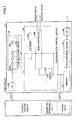
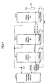
- FIG. 1 is a diagram for explaining an example of the configuration circuit with respect to a single FPGA circuit
- FIG. 2 is a diagram for explaining an example of the configuration circuit with respect to a plurality of FPGA circuits.
- a FPGA circuit (or ROM (Read Only Memory) circuit) 1-1 is formed by a flash memory that stores configuration data "DATA" of a FPGA circuit 2 specified by a user.
- the configuration data "DATA” include parameters, such as a clock frequency (or operation frequency), and circuit data of the FPGA circuit 2.
- the FPGA circuit 2 includes a configuration data memory 21, a FPGA internal circuit 22, an input and output (I/O) buffer 23, a configuration control circuit 24, a clock generating circuit 25, and an I/O buffer 26 that are connected as illustrated in FIG. 1 .
- the configuration control circuit 24 includes a CRC (Cyclic Redundancy Check) circuit 241, a main controller 242, and a decoder 243.
- the clock generating circuit 25 is formed by a ring oscillator that includes a tap adjusting circuit 251 and a plurality of inverter circuits 252 that are connected in series. The clock generating circuit 25 generates a configuration clock signal CLK to be output from the FPGA circuit 2.
- the memory 21 stores set values that determine the logic of the FPGA internal circuit 22, and the set values determine various settings of resources within the FPGA circuit 2.
- the FPGA internal circuit 22 forms a logic function part in which the set values stored in the memory 21 are set.
- the I/O buffer 23 forms an interface usable by a user circuit (not illustrated).
- the CRC circuit 241 detects a data error by comparing a CRC code added to the configuration data "DATA” and a CRC code generated from the configuration data "DATA” read from the configuration circuit 1-1 and input to the FPGA circuit 2, and supplies to the main controller 242 an error detection signal that indicates whether the data error was detected.
- the main controller 242 supplies the clock frequency within the configuration data "DATA” depending on whether the error detection signal indicates that the data error was detected.
- the main controller 242 when no data error is detected and the configuration is successful, the main controller 242 outputs a success signal that indicates that the configuration was successful. On the other hand, when the data error is detected and the configuration fails, the main controller 242 outputs an error signal that indicates that a configuration occurred.
- the decoder 243 decodes the value of the clock frequency, and controls the tap adjusting circuit 251. of the clock generating circuit 25 based on the decoded value, in order to adjust the tap of the inverter circuits 252 and set the frequency of the clock signal CLK generated from the clock generating circuit 25.
- the clock signal CLK is supplied to the configuration control circuit 24, and is also supplied to the configuration circuit 1-1 via the I/O buffer 26.
- a configuration circuit 1-1 is provided with respect to a plurality of FPGA circuits (#1 through #N, where N is a natural number greater than 1) 2-1 through 2-N.
- the FPGA circuit 2-1 functions as a master
- the FPGA circuits 2-2 through 2-N function as slaves.
- the configuration circuit 1-2 inputs the configuration data "DATA" to the master FPGA circuit 2-1, in a manner similar to the configuration circuit 1-1 described above.
- the master FPGA circuit 2-1 supplies the clock signal CLK to the configuration circuit 1-2, in a manner similar to the FPGA circuit 2 described above.
- the clock signal CLK is also supplied to the slave FPGA circuits 2-2 through 2-N.
- the configuration data "DATA" from the configuration circuit 1-2 are successively supplied to the slave FPGA circuits 2-2 through 2-N via the master FPGA circuit 2-1.
- the configuration of the FPGA circuit 2 using the configuration circuit 1-1 illustrated in FIG. 1 may fail.
- the main reason for the failure of the configuration is in most cases a transfer failure or error of the configuration data "DATA", caused by mixing of noise to the configuration data "DATA” and signal decay or deterioration on a printed circuit board (not illustrated) mounted with the FPGA circuit 2.
- the configuration of the FPGA circuit 2 fails, the configuration is in most cases ended as a configuration error.
- the configuration is re-executed under the same conditions as the failed configuration.
- the configuration of the FPGA circuit 2 is performed by providing a frequency setting path from the configuration circuit 1-1 to the clock generating circuit 25 within the FPGA circuit 2, and manually adjusting the value of the clock frequency of the configuration circuit 1-1 in order to manually adjust the set value of the clock frequency of the FPGA circuit 2 by the user.
- This manual adjustment is repeated until the configuration of the FPGA circuit 2 becomes a success, thereby requiring a relatively large number of steps.
- the manual adjustment of the clock frequency is possible, but the manual adjustment of the slew rate is not possible.
- the clock frequency of the configuration of the FPGA circuit is desirably set to a relatively high frequency in order to reduce the configuration time.
- the clock frequency is set to the relatively high frequency, the slew rate of the clock signal becomes relatively high, and it becomes necessary to make a rising edge of the signal sharp.
- layout and wiring information that does not use the defective device may be found by switching a plurality of layout and wiring information prepared in advance, as proposed in a Japanese Laid-Open Patent Publication No. 2005- 243937 , for example.
- this proposed method does not take into consideration the error in the configuration itself of the FPGA circuit.
- a self-configuration function of a programmable device is proposed in a Japanese Laid-Open Patent Publication No. 2000-101421 , for example.
- the plurality of FPGA circuits 2-1 through 2-N may be connected as illustrated in FIG. 2 , and the configuration may fail due to the effects of unpredictable reflection noise or the like, depending on the interconnection or wiring on the circuit board mounted with the FPGA circuits 2-1 through 2-N.
- the conventional configuration of the FPGA circuit requires the manual adjustment of the clock frequency of the FPGA circuit, and there was a problem in that the burden on the use to make the manual adjustment is relatively large.
- a configuration method for performing a configuration of a FPGA (Field Programmable Gate Array) circuit by setting configuration data from a configuration circuit to the FPGA circuit characterized in that the configuration method includes counting, within the FPGA circuit, a number of times a configuration of the FPGA circuit fails; adjusting, within the FPGA circuit, the configuration data at a time when the configuration failed if the counted number exceeds an upper limit value, and re-executing the configuration based on the adjusted configuration data; and setting the configuration data in which the configuration is succeeded from the FPGA circuit to the configuration circuit when the configuration is successful.
- FPGA Field Programmable Gate Array
- a FPGA Field Programmable Gate Array
- a configuration control circuit configured to control a configuration of a FPGA circuit by setting configuration data sent from a configuration circuit to the FPGA circuit, characterized in that the configuration control circuit includes a counter configured to count a number of times a configuration fails; and a main controller configured to adjust the configuration data if the counted number exceeds an upper limit value, and to re-execute the configuration based on the adjusted configuration data, wherein the main controller sets the configuration data at a time when the configuration is successful from the FPGA circuit to the configuration circuit.
- the configuration control circuit includes a counter configured to count a number of times a configuration fails; and a main controller configured to adjust the configuration data if the counted number exceeds an upper limit value, and to re-execute the configuration based on the adjusted configuration data, wherein the main controller sets the configuration data at a time when the configuration is successful from the FPGA circuit to the configuration circuit.
- configuration data of the FPGA circuit such as a clock frequency (or operation frequency) and slew rate of a FPGA circuit
- the configuration data that cause a successful configuration of the FPGA circuit may be automatically adjusted by the FPGA circuit without requiring manual adjustment by a user, that is without requiring the user to be aware of the adjustment of the configuration data.
- the adjustment cost of the configuration may be suppressed to a relatively low cost.
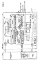
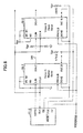
- FIG. 3 is a diagram for explaining an example of a configuration circuit in a first embodiment of the present invention.
- the present invention is applied to a case where the configuration circuit is provided with respect to a single FPGA circuit.
- blocks indicated by bold solid lines denote functional blocks that may perform the automatic adjustment using a path indicated by bold solid lines and store the settings using a path indicated by double solid lines.
- a configuration circuit (or ROM (Read Only Memory) circuit) 51-1 is formed by a flash memory that stores configuration data "DATA" of a FPGA circuit 52 specified by the user.
- the configuration data "DATA" include parameters, such as the clock frequency (or operation frequency) and slew rate, and circuit data of the FPGA circuit 52.
- the clock frequency refers to the frequency of a clock signal CLK that will be described later
- the slew rate refers to the slew rate of the clock signal CLK.
- the FPGA circuit 52 includes an input and output (I/O) buffer 61, a configuration data memory 62, a FPGA internal circuit 63, I/0 buffers 64 and 65, a configuration control circuit 66, an I/O buffer 67, a clock generating circuit 68, and an I/O buffer 69 that are connected as illustrated in FIG. 3 .
- the configuration control circuit 66 includes a CRC (Cyclic Redundancy Check) circuit 661, a counter 662, a main controller 663, a slew rate store part 664, a decoder 665, a clock frequency store part 666, and a decoder 667.
- CRC Cyclic Redundancy Check
- the main controller 663 includes a transfer data store part 71, an error detection circuit 72, a comparator circuit 73, and a decoder 74.
- the clock generating circuit 68 is formed by a ring oscillator that includes a tap adjusting circuit 681 and a plurality of inverter circuits 682 that are connected in series.
- the clock generating circuit 68 generates the configuration clock signal CLK to be output from the FPGA circuit 52.
- the I/O buffer 61 supplies to the configuration control circuit 66 configuration data "DATA1" read from the configuration circuit 51-1 and input to the FPGA circuit 52 in synchronism with the clock signal CLK.
- the memory 61 stores set values that determine the logic of the FPGA internal circuit 63, and the set values determine various settings of resources within the FPGA circuit 52.
- the FPGA internal circuit 63 forms a logic function part in which the set values stored in the memory 62 are set.
- the I/O buffer 64 may output the configuration data at the time when the configuration is successful to the FPGA circuit of the next stage, as configuration data "DATA-1".
- the I/O buffer 65 forms an interface usable by a user circuit (not illustrated) external to the FPGA circuit 52.
- the CRC circuit 661 detects a data error by comparing a CRC code added to the configuration data "DATA1” and a CRC code generated from the configuration data "DATA1” read from the configuration circuit 51-1 and input to the FPGA circuit 52 in synchronism with the clock signal CLK, and supplies to the error detection circuit 72 within the main controller 663 an error detection signal that indicates whether the data error was detected.
- the error detection signal may be output to the FPGA circuit of the next stage or the user circuit.
- the error detection signal may be used in the FPGA circuit of the next stage or the user circuit as a success signal that indicates that the configuration was successful.
- the CRC circuit 661 supplies the configuration data "DATA1" to the transfer data store part 71 within the main controller 663.
- the counter 662 counts a re-execution number n' (n is a natural number greater than or equal to 0) that indicates the number of times the configuration is repeated due to the generation of the configuration error (or failure of the configuration).
- a slew rate t stored in the slew rate store part 664 and a clock frequency f stored in the clock frequency store part 666 are supplied to the transfer data store part 71 within the main controller 663.
- the transfer data store part 71 stores the configuration data at the time when the configuration was successful, such as the clock frequency f and slew rate t, to the configuration circuit 51-1 via the I/O buffer 67, as new configuration data "DATA2".
- the configuration data "DATA1" are automatically adjusted by the configuration control circuit 66, and the more optimized configuration data "DATA2" is automatically set in the configuration circuit 51-1.
- the configuration data "DATA2" that are automatically set in the configuration circuit 51-1 become usable when performing the next configuration.
- the error detection circuit 72 detects whether the configuration error exists, based on the error detection signal from the CRC circuit 661, and notifies an error detection result to the comparator circuit 73 and the counter 662. In addition, when the error detection circuit 72 detects the configuration error, the error detection circuit 72 modifies, that is automatically adjusts, the clock frequency f stored in the clock frequency store part 666 and the slew rate t stored in the slew rate store part 664, according to a preset rule. For example, the clock frequency f is lowered according to the rule, and the slew rate t is reduced according to the rule.
- the error detection circuit 72 judges that the configuration was successful, and supplies the slew rate t within the configuration data "DATA1" to the slew rate store part 664, and supplies the clock frequency f within the configuration data "DATA1" to the clock frequency store part 666.
- the decoder 74 receives an external input of a set signal indicating an upper limit value R of the repetition of the configuration, and inputs to the comparator circuit 73 the upper limit value R that is obtained by decoding the set signal. In other words, the decoder 74 decodes the set signal into the upper limit value R having a format referable (or accessible) within the FPGA circuit 52 (or within the main controller 663).
- the comparator circuit 73 compares the upper limit value R and the counted value (or re-execution number) n of the counter 662. If the re-execution number n exceeds the upper limit value R, the comparator circuit 73 notifies the generation of a configuration error in which the re-execution number n exceeds the upper limit value R, by outputting an error status signal indicating this configuration error.
- the clock frequency f stored in the clock frequency store part 666 may be supplied from the I/O buffer 61.
- the upper limit value R may be supplied to the comparator circuit 73 from the I/O buffer 61.
- the clock frequency f stored in the clock frequency store part 666 is decoded by the decoder 667.
- the tap adjusting circuit 681 of the clock generating circuit 68 is controlled based on a decoded value output from the decoder 667, in order to set the clock frequency f of the clock signal CLK that is generated from the clock generating circuit 68.
- the clock signal CLK is supplied to the configuration control circuit 66, and is also supplied to the configuration circuit 51-1 via the I/O buffer 69.
- the slew rate t stored in the slew rate store part 664 is decoder by the decoder 665. A timing at which the clock signal CLK is supplied from the I/O buffer 69 to the configuration circuit 51-1 is controlled based on a decoded value output from the decoder 665, depending on the setting of the slew rate t.
- the configuration success signal output from the FPGA circuit of the next stage may be input to the configuration control circuit 66 (or the main controller 663), in order to enable the FPGA circuit 52 to recognize whether the configuration was successful in the FPGA circuit of the next stage.
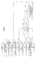
- FIG. 4 is a flow chart for explaining a configuration process executed within the FPGA circuit 52.
- a step S1 sets the upper limit value R of the re-execution number n for the case where the configuration fails, and sets the re-execution number n to an initial value "1".
- the upper limit value R may be set from outside the FPGA circuit 52 or, may be set from the configuration circuit 51-1.
- a step S2 sets the clock frequency f that is to be used at the time of the configuration of the FPGA circuit 52, and a step S3 sets the slew rate t that is used at the time of the configuration.
- Initial values of the clock frequency f and the slew rate t may be values set in the configuration circuit 51-1.
- a step S4 executes the configuration of the FPGA circuit 52.
- the configuration is executed during operation of the FPGA circuit 52, for example.
- a step S5 judges, in the configuration control circuit 66, whether the configuration was successful. If the configuration was successful and the judgement result in the step S5 is YES, a step S10 sets a success flag, indicating that the configuration was successful, to "1".
- a step S11 judges whether the clock frequency f and the slew rate t are stored in the clock frequency store part 666 and the slew rate store part 664, respectively. If the judgement result in the step S11 is YES, a step S12 stores in the configuration circuit 51-1 the clock frequency f stored in the clock frequency store part 666 and the slew rate t stored in the slew rate store part 664, an the process ends. On the other hand, if the judgement result in the step S11 is NO, the process ends.
- the step S4 executes the configuration, and the re-execution of the configuration and the automatic adjustment of the configuration data are repeated until the configuration becomes a success or, the configuration fails and the re-execution number n of the configuration exceeds the upper limit value R.
- the clock frequency f is automatically adjusted to a value that is 10% lower, for example, because the cause of the configuration failure may be an excessively high clock frequency f.
- the slew rate t is automatically adjusted to a value that is reduced by 10%, because the cause of the configuration failure may be an excessively high slew rate t.
- the clock frequency f and the slew rate t are automatically adjusted by combining the first and second examples described above.
- a path is provided from the error detection circuit 72 of the main controller 663 to the clock generating circuit 68 and the I/O buffer 69, within the configuration control circuit 66 of the FPGA circuit 52 illustrated in FIG. 3 , in order to provide a mechanism to re-execute the configuration by automatically adjusting the clock frequency f and the slew rate t.
- a path is provided to the I/O buffer 67 from the main controller 663, the clock frequency store part 666, and the slew rate store part 664 within the configuration control circuit 66 illustrated in FIG. 3 , in order to provide a mechanism to store and set the clock frequency f and the slew rate t at the time when the configuration was successful within the configuration circuit 51-1.
- the cost of manually adjusting the configuration data "DATA1" for each FPGA product including the FPGA circuit 52 may be reduced.
- the FPGA circuit 52 itself automatically adjusts the configuration data and controls the configuration to a success, and it is unnecessary for the user to manually adjust and manually set the optimum clock frequency and slew rate in order to control the configuration to the success.
- the optimum clock frequency or slew rate for controlling the configuration to the success changes due to a change in an operating environment in which the FPGA circuit 52 operates, such as the ambient temperature of the FPGA circuit 52, the user does not need to be aware of such changes because the FPGA circuit 52 itself automatically adjusts and automatically sets the configuration data.
- the optimum clock frequency and slew rate at the time when the configuration was successful are automatically set in the configuration circuit 51-1, the next configuration may be performed using the optimum clock frequency and slew rate in order to suppress the configuration error.
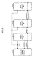
- FIG. 5 is a diagram for explaining an example of the configuration circuit in a second embodiment of the present invention.
- the present invention is applied to a case where the configuration circuit is provided with respect to a plurality of FPGA circuits.
- a configuration circuit 51-2 is provided with respect to a plurality of FPGA circuits (#1 through #N, where N is a natural number greater than 1) 52-1 through 52-N.
- the FPGA circuit 52-1 functions as a master
- the FPGA circuits 52-2 through 52-N function as slaves.
- the configuration circuit 51-2 inputs the configuration data "DATA1" to the master FPGA circuit 52-1, in a manner similar to the configuration circuit 51-1 described above.
- the master FPGA circuit 52-1 supplies the clock signal CLK to the configuration circuit 51-2, in a manner similar to the FPGA circuit 52 described above.
- the clock signal CLK is also supplied to the slave FPGA circuits 52-2 through 52-N.
- the configuration data "DATA1" from the configuration circuit 51-2 are successively supplied to the slave FPGA circuits 52-2 through 52-N via the master FPGA circuit 52-1, as configuration data "DATA1-1" through "DATA1-N-1".
- FIG. 6 is a diagram illustrating a structure of the configuration control circuit in the second embodiment.
- the FPGA circuit 52-1 has the same structure as the FPGA circuit 52 illustrated in FIG. 3
- the configuration process executed within the FPGA circuit 52-1 is the same as that illustrated in the flow chart of FIG. 4 . Accordingly, in FIG. 6 , those parts that are the same as those corresponding parts in FIG. 3 are designated by the same reference numerals, and a description thereof will be omitted.
- circuit parts within the FPGA circuit 52-2 represented by halftone shades indicate function parts that may be unused, unlike the FPGA circuit 52-1.
- input and output signals that may be unused are labeled as "unused” in FIG. 6 .
- a transfer direction of the clock signal CLK with respect to the I/O buffer 69 within the FPGA circuit 52-2 is opposite to that with respect to the I/O buffer 69 within the FPGA circuit 52-1.
- the operation of the FPGA circuit 52-2 is basically the same as the operation of the FPGA circuit 52-1.
- Configuration data "DATA1-2" output from the I/O buffer 64 within the FPGA circuit 52-2 is supplied to the I/O buffer 61 within the FPGA circuit 52-3 (not illustrated) of the next stage.
- each of the slave FPGA circuits 52-2 through 52-N operate in synchronism with the clock signal CLK that is output from the master FPGA circuit 52-1, and the slave FPGA circuit 52-i (i is a natural number greater than or equal to 2) is supplied with the configuration data that passed through the FPGA circuit 52-i-1 of the preceding stage. As illustrated in FIG.
- the configuration data "DATA1-1" output from the master FPGA circuit 52-1 are supplied to the slave FPGA circuit 52-2 of the next stage, and the configuration data "DATA1-2” output from the slave FPGA circuit 52-2 are supplied to the slave FPGA circuit 52-3 (not illustrated) of the next stage, ..., and the configuration data "DATA1-N-1" output from the slave FPGA circuit 52-N-1 are supplied to the slave FPGA circuit 52-N of the next stage.
- FIG. 7 is a diagram for explaining outputting of a configuration success signal in the second embodiment.
- those parts that are the same as those corresponding parts in FIG. 5 are designated by the same reference numerals, and a description thereof will be omitted.
- FIG. 7 illustrates a transfer path of the configuration success signal, the illustration of which is omitted in FIG. 5 .
- FIG. 7 illustrates a case where the configuration success signal is an open-drain signal.
- the configuration success signal output from each of the FPGA circuits 52-1 through 52-N is input to the main controller 663 within the FPGA circuit 52-1 of the first stage via a signal line 530.
- the signal line 530 is connected to a power supply voltage Vcc via a pull-up resistor 631.
- the parts other than the master FPGA circuit 52-1, including the slave FPGA circuits 52-2 through 52-N, may be connected using various other connecting methods or arrangement.
- FIG. 8 is a diagram illustrating a first example of the connection of the slave FPGA circuits.
- FIG. 8 only illustrates the configuration circuit 51-2, the master FPGA circuit 52-1, and the slave FFGA circuit 52-2.
- the configuration circuit 51-2 may be formed by a PROM (Programmable ROM) manufactured by Xilinx, Inc.
- the master FPGA circuit 52-1 and the slave FPGA circuit 52-2 may be formed by Virtex-5 family (or series) FPGAs manufactured by Xilinx, Inc., and thus, the illustration of all of the terminals is omitted in FIG. 8 .
- a signal /PROGRAM instructs the start of the configuration.
- the a data bus 541 that connects the master FPGA circuit 52-1 and the slave FPGA circuit 52-2 and transfer the configuration data is formed by a serial bus.
- FIG. 9 is a diagram illustrating a second example of the connection of the slave FPGA circuits.
- FIG. 9 only illustrates the configuration circuit 51-2, the master FPGA circuit 52-1, and the slave FPGA circuits 52-2 and 52-3.
- the configuration circuit 51-2 may be formed by a flash memory manufactured by Xilinx, Inc.
- the master FPGA circuit 52-1 and the slave FPGA circuits 52-2 and 52-3 may be formed by Virtex-5 family (or series) FPGAs manufactured by Xilinx, Inc., and thus, the illustration of all of the terminals is omitted in FIG. 9 .
- the data buses 542 that connect the master FPGA circuit 52-1 and the slave FPGA circuits 52-2 and 52-3 and transfer the configuration data are formed by parallel buses.
- an error detection signal output from a CSO_B terminal of the master FPGA circuit 52-1 indicates that a successful configuration
- the configuration process of the slave FPGA circuit 52-2 that receives the error detection signal at a CS_B terminal thereof starts.
- the FPGA circuit 52-1 itself automatically adjusts the configuration data and controls the configuration to a success, and it is unnecessary for the user to manually adjust and manually set the optimum clock frequency and slew rate in order to control the configuration to the success, even when the FPGA circuits 52-1 through 52-N are connected in a plurality of stages.
- the advantageous effects obtainable in the first embodiment described above may also be obtained in this embodiment.
Landscapes
- Physics & Mathematics (AREA)
- Mathematical Physics (AREA)
- Engineering & Computer Science (AREA)
- Computer Hardware Design (AREA)
- Computing Systems (AREA)
- General Engineering & Computer Science (AREA)
- Logic Circuits (AREA)
- Design And Manufacture Of Integrated Circuits (AREA)
- Retry When Errors Occur (AREA)
- Stored Programmes (AREA)
Applications Claiming Priority (1)
| Application Number | Priority Date | Filing Date | Title |
|---|---|---|---|
| JP2010056298A JP5609176B2 (ja) | 2010-03-12 | 2010-03-12 | コンフィグレーション方法及びコンフィグレーション制御回路 |
Publications (2)
| Publication Number | Publication Date |
|---|---|
| EP2365632A2 true EP2365632A2 (de) | 2011-09-14 |
| EP2365632A3 EP2365632A3 (de) | 2013-09-25 |
Family
ID=44237450
Family Applications (1)
| Application Number | Title | Priority Date | Filing Date |
|---|---|---|---|
| EP11157593.2A Withdrawn EP2365632A3 (de) | 2010-03-12 | 2011-03-10 | Konfigurationsverfahren und FPGA-Schaltung |
Country Status (3)
| Country | Link |
|---|---|
| US (1) | US8436644B2 (de) |
| EP (1) | EP2365632A3 (de) |
| JP (1) | JP5609176B2 (de) |
Families Citing this family (12)
| Publication number | Priority date | Publication date | Assignee | Title |
|---|---|---|---|---|
| US8839051B1 (en) * | 2011-02-25 | 2014-09-16 | Sk Hynix Memory Solutions Inc. | Advance clocking scheme for ECC in storage |
| US8719646B2 (en) * | 2012-04-30 | 2014-05-06 | Freescale Semiconductor, Inc. | Non-volatile memory (NVM) reset sequence with built-in read check |
| US9542244B2 (en) | 2015-04-22 | 2017-01-10 | Ryft Systems, Inc. | Systems and methods for performing primitive tasks using specialized processors |
| US9411613B1 (en) | 2015-04-22 | 2016-08-09 | Ryft Systems, Inc. | Systems and methods for managing execution of specialized processors |
| US9411528B1 (en) | 2015-04-22 | 2016-08-09 | Ryft Systems, Inc. | Storage management systems and methods |
| KR20180081732A (ko) * | 2015-11-13 | 2018-07-17 | 가부시키가이샤 한도오따이 에네루기 켄큐쇼 | 반도체 장치, 전자 부품, 및 전자 기기 |
| CN105930284A (zh) * | 2016-04-14 | 2016-09-07 | 青岛海信电器股份有限公司 | 一种fpga加载的方法和设备 |
| JP2019096960A (ja) * | 2017-11-20 | 2019-06-20 | 富士通株式会社 | 伝送装置及び伝送方法 |
| US11157346B2 (en) * | 2018-09-26 | 2021-10-26 | Palo Alto Rsearch Center Incorporated | System and method for binned inter-quartile range analysis in anomaly detection of a data series |
| US10572430B2 (en) * | 2018-10-11 | 2020-02-25 | Intel Corporation | Methods and apparatus for programming an integrated circuit using a configuration memory module |
| KR102736619B1 (ko) | 2019-08-27 | 2024-12-02 | 삼성전자주식회사 | 무선 통신 시스템에서 다중 fpga를 운영하기 위한 장치 및 방법 |
| CN119621656A (zh) * | 2025-02-13 | 2025-03-14 | 中科亿海微电子科技(苏州)有限公司 | 一种多块级联的可编程器件的配置方法和系统 |
Citations (2)
| Publication number | Priority date | Publication date | Assignee | Title |
|---|---|---|---|---|
| JP2001001421A (ja) | 1999-06-17 | 2001-01-09 | Nippon Paper Industries Co Ltd | 液体用紙容器用の充填機のボトムヒートシール装置に備えられるプレッシャーパッド |
| JP2005243937A (ja) | 2004-02-26 | 2005-09-08 | Fujitsu Ltd | 集積回路装置設計方法、当該方法を実施可能なデータ処理装置及びプログラム |
Family Cites Families (18)
| Publication number | Priority date | Publication date | Assignee | Title |
|---|---|---|---|---|
| US5590305A (en) * | 1994-03-28 | 1996-12-31 | Altera Corporation | Programming circuits and techniques for programming logic |
| JP2000101421A (ja) * | 1998-09-22 | 2000-04-07 | Fujitsu Ltd | プログラマブルデバイス |
| US6535986B1 (en) * | 2000-03-14 | 2003-03-18 | International Business Machines Corporation | Optimizing performance of a clocked system by adjusting clock control settings and clock frequency |
| JP3938308B2 (ja) * | 2001-12-28 | 2007-06-27 | 富士通株式会社 | プログラマブル論理デバイス |
| EP1411431A3 (de) * | 2002-09-20 | 2010-10-20 | Sicronic Remote KG, LLC | Verfahren und Gerät zum herladen von fehlerhafte Konfigurationsdaten während Konfiguration von PLD's |
| JP2004272406A (ja) * | 2003-03-06 | 2004-09-30 | Meidensha Corp | 同期転送速度の自動調整方法 |
| US7324590B2 (en) * | 2003-05-28 | 2008-01-29 | Qualcomm Incoporated | Equalizer with combined CCK encoding-decoding in feedback filtering of decision feedback equalizer |
| US6870390B1 (en) * | 2003-09-11 | 2005-03-22 | Xilinx, Inc. | Tx line driver with common mode idle state and selectable slew rates |
| JP4028480B2 (ja) * | 2003-12-25 | 2007-12-26 | 富士通株式会社 | Fpgaコンフィギュレーション制御方法及び制御装置 |
| US7343579B2 (en) * | 2004-11-30 | 2008-03-11 | Physical Sciences | Reconfigurable environmentally adaptive computing |
| JP4626349B2 (ja) * | 2005-03-18 | 2011-02-09 | コニカミノルタホールディングス株式会社 | ハードウェアコンフィグレーション装置 |
| US7397272B1 (en) * | 2006-02-28 | 2008-07-08 | Xilinx, Inc. | Parallel configuration of programmable devices |
| JP2007265056A (ja) * | 2006-03-29 | 2007-10-11 | Juki Corp | プログラマブルロジックデバイスのコンフィギュレーション装置 |
| JP2008103996A (ja) * | 2006-10-19 | 2008-05-01 | Renesas Technology Corp | 半導体集積回路装置 |
| US7576557B1 (en) * | 2008-03-26 | 2009-08-18 | Xilinx, Inc. | Method and apparatus for mitigating one or more event upsets |
| US7746699B1 (en) * | 2008-09-11 | 2010-06-29 | Xilinx, Inc. | Non-volatile memory read-check |
| KR101653206B1 (ko) * | 2010-01-19 | 2016-09-02 | 삼성전자주식회사 | 프로그램 검증 회로 및 이를 포함하는 비휘발성 메모리 장치 |
| US8332722B1 (en) * | 2010-08-11 | 2012-12-11 | Microelectronics Research and Development Corporation | Method and architecture for performing scrubbing of an FPGA's configuration memory |
-
2010
- 2010-03-12 JP JP2010056298A patent/JP5609176B2/ja not_active Expired - Fee Related
-
2011
- 2011-03-10 EP EP11157593.2A patent/EP2365632A3/de not_active Withdrawn
- 2011-03-11 US US13/064,236 patent/US8436644B2/en not_active Expired - Fee Related
Patent Citations (2)
| Publication number | Priority date | Publication date | Assignee | Title |
|---|---|---|---|---|
| JP2001001421A (ja) | 1999-06-17 | 2001-01-09 | Nippon Paper Industries Co Ltd | 液体用紙容器用の充填機のボトムヒートシール装置に備えられるプレッシャーパッド |
| JP2005243937A (ja) | 2004-02-26 | 2005-09-08 | Fujitsu Ltd | 集積回路装置設計方法、当該方法を実施可能なデータ処理装置及びプログラム |
Also Published As
| Publication number | Publication date |
|---|---|
| JP2011193129A (ja) | 2011-09-29 |
| US8436644B2 (en) | 2013-05-07 |
| JP5609176B2 (ja) | 2014-10-22 |
| US20110227605A1 (en) | 2011-09-22 |
| EP2365632A3 (de) | 2013-09-25 |
Similar Documents
| Publication | Publication Date | Title |
|---|---|---|
| US8436644B2 (en) | Configuration method and FPGA circuit re-executing configuration based on adjusted configuration data | |
| US20190272252A1 (en) | Method of processing deadlock of i2c bus, electronic device and communication system | |
| US7622961B2 (en) | Method and apparatus for late timing transition detection | |
| US8648645B2 (en) | Microprocessor performance and power optimization through self calibrated inductive voltage droop monitoring and correction | |
| US7818699B1 (en) | Dynamic core pipeline | |
| US10033357B2 (en) | Semiconductor device | |
| WO2009035950A1 (en) | Area and power saving standard cell methodology | |
| KR20150119546A (ko) | 반도체 장치 | |
| US20200152261A1 (en) | Methods and apparatus for reduced area control register circuit | |
| US8108754B1 (en) | Programmable logic device programming verification systems and methods | |
| US10580467B2 (en) | Memory interface and memory system including plurality of delay adjustment circuits shared by memory read and write circuits for adjusting the timing of read and write data signals | |
| EP4446758A1 (de) | Integrierte schaltung mit zeitkorrekturschaltung | |
| CN113467570B (zh) | 一种usb全速设备芯片的时钟精确校准系统和方法 | |
| US20090302887A1 (en) | Apparatus for power consumption reduction in programmable logic devices and associated methods | |
| JP2005234976A (ja) | 記憶装置 | |
| US7956661B2 (en) | Standard cell and semiconductor device | |
| US7795909B1 (en) | High speed programming of programmable logic devices | |
| US5087953A (en) | Flexible gate array system for combinatorial logic | |
| US20170019113A1 (en) | Semiconductor device and method for controlling the semiconductor device | |
| US9621167B2 (en) | Logic circuit and method for controlling a setting circuit | |
| EP4202708A1 (de) | Integrierte schaltung für eine grosse berührungsanzeige und betriebsverfahren dafür | |
| US20100219869A1 (en) | Semiconductor intergrated circuit and signal adjusting method | |
| KR101453176B1 (ko) | 정보 처리 장치 또는 정보 처리 방법 | |
| US11404334B1 (en) | Testing circuit with shared testing pads located on the scribe line and testing method thereof | |
| JP4510052B2 (ja) | 半導体集積回路装置及びデューティ制御方法 |
Legal Events
| Date | Code | Title | Description |
|---|---|---|---|
| PUAI | Public reference made under article 153(3) epc to a published international application that has entered the european phase |
Free format text: ORIGINAL CODE: 0009012 |
|
| AK | Designated contracting states |
Kind code of ref document: A2 Designated state(s): AL AT BE BG CH CY CZ DE DK EE ES FI FR GB GR HR HU IE IS IT LI LT LU LV MC MK MT NL NO PL PT RO RS SE SI SK SM TR |
|
| AX | Request for extension of the european patent |
Extension state: BA ME |
|
| PUAL | Search report despatched |
Free format text: ORIGINAL CODE: 0009013 |
|
| AK | Designated contracting states |
Kind code of ref document: A3 Designated state(s): AL AT BE BG CH CY CZ DE DK EE ES FI FR GB GR HR HU IE IS IT LI LT LU LV MC MK MT NL NO PL PT RO RS SE SI SK SM TR |
|
| AX | Request for extension of the european patent |
Extension state: BA ME |
|
| RIC1 | Information provided on ipc code assigned before grant |
Ipc: H03K 19/00 20060101AFI20130822BHEP Ipc: H03K 19/177 20060101ALI20130822BHEP |
|
| 17P | Request for examination filed |
Effective date: 20140219 |
|
| RBV | Designated contracting states (corrected) |
Designated state(s): AL AT BE BG CH CY CZ DE DK EE ES FI FR GB GR HR HU IE IS IT LI LT LU LV MC MK MT NL NO PL PT RO RS SE SI SK SM TR |
|
| 17Q | First examination report despatched |
Effective date: 20140403 |
|
| STAA | Information on the status of an ep patent application or granted ep patent |
Free format text: STATUS: THE APPLICATION IS DEEMED TO BE WITHDRAWN |
|
| 18D | Application deemed to be withdrawn |
Effective date: 20151001 |