EP2365531B1 - Semiconductor device and power conversion apparatus using the same - Google Patents
Semiconductor device and power conversion apparatus using the same Download PDFInfo
- Publication number
- EP2365531B1 EP2365531B1 EP10015210.7A EP10015210A EP2365531B1 EP 2365531 B1 EP2365531 B1 EP 2365531B1 EP 10015210 A EP10015210 A EP 10015210A EP 2365531 B1 EP2365531 B1 EP 2365531B1
- Authority
- EP
- European Patent Office
- Prior art keywords
- layer
- insulating layer
- semiconductor
- semiconductor layer
- gate
- Prior art date
- Legal status (The legal status is an assumption and is not a legal conclusion. Google has not performed a legal analysis and makes no representation as to the accuracy of the status listed.)
- Active
Links
Images













Classifications
-
- H—ELECTRICITY
- H10—SEMICONDUCTOR DEVICES; ELECTRIC SOLID-STATE DEVICES NOT OTHERWISE PROVIDED FOR
- H10D—INORGANIC ELECTRIC SEMICONDUCTOR DEVICES
- H10D12/00—Bipolar devices controlled by the field effect, e.g. insulated-gate bipolar transistors [IGBT]
- H10D12/411—Insulated-gate bipolar transistors [IGBT]
- H10D12/441—Vertical IGBTs
-
- H—ELECTRICITY
- H10—SEMICONDUCTOR DEVICES; ELECTRIC SOLID-STATE DEVICES NOT OTHERWISE PROVIDED FOR
- H10D—INORGANIC ELECTRIC SEMICONDUCTOR DEVICES
- H10D12/00—Bipolar devices controlled by the field effect, e.g. insulated-gate bipolar transistors [IGBT]
- H10D12/01—Manufacture or treatment
- H10D12/031—Manufacture or treatment of IGBTs
- H10D12/032—Manufacture or treatment of IGBTs of vertical IGBTs
- H10D12/038—Manufacture or treatment of IGBTs of vertical IGBTs having a recessed gate, e.g. trench-gate IGBTs
-
- H—ELECTRICITY
- H10—SEMICONDUCTOR DEVICES; ELECTRIC SOLID-STATE DEVICES NOT OTHERWISE PROVIDED FOR
- H10D—INORGANIC ELECTRIC SEMICONDUCTOR DEVICES
- H10D12/00—Bipolar devices controlled by the field effect, e.g. insulated-gate bipolar transistors [IGBT]
- H10D12/411—Insulated-gate bipolar transistors [IGBT]
- H10D12/441—Vertical IGBTs
- H10D12/461—Vertical IGBTs having non-planar surfaces, e.g. having trenches, recesses or pillars in the surfaces of the emitter, base or collector regions
- H10D12/481—Vertical IGBTs having non-planar surfaces, e.g. having trenches, recesses or pillars in the surfaces of the emitter, base or collector regions having gate structures on slanted surfaces, on vertical surfaces, or in grooves, e.g. trench gate IGBTs
-
- H—ELECTRICITY
- H10—SEMICONDUCTOR DEVICES; ELECTRIC SOLID-STATE DEVICES NOT OTHERWISE PROVIDED FOR
- H10D—INORGANIC ELECTRIC SEMICONDUCTOR DEVICES
- H10D62/00—Semiconductor bodies, or regions thereof, of devices having potential barriers
- H10D62/10—Shapes, relative sizes or dispositions of the regions of the semiconductor bodies; Shapes of the semiconductor bodies
- H10D62/102—Constructional design considerations for preventing surface leakage or controlling electric field concentration
- H10D62/103—Constructional design considerations for preventing surface leakage or controlling electric field concentration for increasing or controlling the breakdown voltage of reverse-biased devices
- H10D62/105—Constructional design considerations for preventing surface leakage or controlling electric field concentration for increasing or controlling the breakdown voltage of reverse-biased devices by having particular doping profiles, shapes or arrangements of PN junctions; by having supplementary regions, e.g. junction termination extension [JTE]
-
- H—ELECTRICITY
- H10—SEMICONDUCTOR DEVICES; ELECTRIC SOLID-STATE DEVICES NOT OTHERWISE PROVIDED FOR
- H10D—INORGANIC ELECTRIC SEMICONDUCTOR DEVICES
- H10D64/00—Electrodes of devices having potential barriers
- H10D64/111—Field plates
- H10D64/117—Recessed field plates, e.g. trench field plates or buried field plates
-
- H—ELECTRICITY
- H10—SEMICONDUCTOR DEVICES; ELECTRIC SOLID-STATE DEVICES NOT OTHERWISE PROVIDED FOR
- H10D—INORGANIC ELECTRIC SEMICONDUCTOR DEVICES
- H10D64/00—Electrodes of devices having potential barriers
- H10D64/20—Electrodes characterised by their shapes, relative sizes or dispositions
- H10D64/23—Electrodes carrying the current to be rectified, amplified, oscillated or switched, e.g. sources, drains, anodes or cathodes
- H10D64/251—Source or drain electrodes for field-effect devices
- H10D64/252—Source or drain electrodes for field-effect devices for vertical or pseudo-vertical devices
-
- H—ELECTRICITY
- H10—SEMICONDUCTOR DEVICES; ELECTRIC SOLID-STATE DEVICES NOT OTHERWISE PROVIDED FOR
- H10D—INORGANIC ELECTRIC SEMICONDUCTOR DEVICES
- H10D64/00—Electrodes of devices having potential barriers
- H10D64/20—Electrodes characterised by their shapes, relative sizes or dispositions
- H10D64/23—Electrodes carrying the current to be rectified, amplified, oscillated or switched, e.g. sources, drains, anodes or cathodes
- H10D64/251—Source or drain electrodes for field-effect devices
- H10D64/252—Source or drain electrodes for field-effect devices for vertical or pseudo-vertical devices
- H10D64/2527—Source or drain electrodes for field-effect devices for vertical or pseudo-vertical devices for vertical devices wherein the source or drain electrodes are recessed in semiconductor bodies
-
- H—ELECTRICITY
- H10—SEMICONDUCTOR DEVICES; ELECTRIC SOLID-STATE DEVICES NOT OTHERWISE PROVIDED FOR
- H10D—INORGANIC ELECTRIC SEMICONDUCTOR DEVICES
- H10D64/00—Electrodes of devices having potential barriers
- H10D64/20—Electrodes characterised by their shapes, relative sizes or dispositions
- H10D64/23—Electrodes carrying the current to be rectified, amplified, oscillated or switched, e.g. sources, drains, anodes or cathodes
- H10D64/251—Source or drain electrodes for field-effect devices
- H10D64/256—Source or drain electrodes for field-effect devices for lateral devices wherein the source or drain electrodes are recessed in semiconductor bodies
-
- H—ELECTRICITY
- H10—SEMICONDUCTOR DEVICES; ELECTRIC SOLID-STATE DEVICES NOT OTHERWISE PROVIDED FOR
- H10D—INORGANIC ELECTRIC SEMICONDUCTOR DEVICES
- H10D64/00—Electrodes of devices having potential barriers
- H10D64/20—Electrodes characterised by their shapes, relative sizes or dispositions
- H10D64/27—Electrodes not carrying the current to be rectified, amplified, oscillated or switched, e.g. gates
- H10D64/311—Gate electrodes for field-effect devices
- H10D64/411—Gate electrodes for field-effect devices for FETs
- H10D64/511—Gate electrodes for field-effect devices for FETs for IGFETs
- H10D64/512—Disposition of the gate electrodes, e.g. buried gates
- H10D64/513—Disposition of the gate electrodes, e.g. buried gates within recesses in the substrate, e.g. trench gates, groove gates or buried gates
-
- H—ELECTRICITY
- H10—SEMICONDUCTOR DEVICES; ELECTRIC SOLID-STATE DEVICES NOT OTHERWISE PROVIDED FOR
- H10D—INORGANIC ELECTRIC SEMICONDUCTOR DEVICES
- H10D64/00—Electrodes of devices having potential barriers
- H10D64/20—Electrodes characterised by their shapes, relative sizes or dispositions
- H10D64/27—Electrodes not carrying the current to be rectified, amplified, oscillated or switched, e.g. gates
- H10D64/311—Gate electrodes for field-effect devices
- H10D64/411—Gate electrodes for field-effect devices for FETs
- H10D64/511—Gate electrodes for field-effect devices for FETs for IGFETs
- H10D64/517—Gate electrodes for field-effect devices for FETs for IGFETs characterised by the conducting layers
- H10D64/518—Gate electrodes for field-effect devices for FETs for IGFETs characterised by the conducting layers characterised by their lengths or sectional shapes
-
- H—ELECTRICITY
- H10—SEMICONDUCTOR DEVICES; ELECTRIC SOLID-STATE DEVICES NOT OTHERWISE PROVIDED FOR
- H10D—INORGANIC ELECTRIC SEMICONDUCTOR DEVICES
- H10D62/00—Semiconductor bodies, or regions thereof, of devices having potential barriers
- H10D62/10—Shapes, relative sizes or dispositions of the regions of the semiconductor bodies; Shapes of the semiconductor bodies
- H10D62/102—Constructional design considerations for preventing surface leakage or controlling electric field concentration
-
- H—ELECTRICITY
- H10—SEMICONDUCTOR DEVICES; ELECTRIC SOLID-STATE DEVICES NOT OTHERWISE PROVIDED FOR
- H10D—INORGANIC ELECTRIC SEMICONDUCTOR DEVICES
- H10D62/00—Semiconductor bodies, or regions thereof, of devices having potential barriers
- H10D62/10—Shapes, relative sizes or dispositions of the regions of the semiconductor bodies; Shapes of the semiconductor bodies
- H10D62/102—Constructional design considerations for preventing surface leakage or controlling electric field concentration
- H10D62/103—Constructional design considerations for preventing surface leakage or controlling electric field concentration for increasing or controlling the breakdown voltage of reverse-biased devices
-
- H—ELECTRICITY
- H10—SEMICONDUCTOR DEVICES; ELECTRIC SOLID-STATE DEVICES NOT OTHERWISE PROVIDED FOR
- H10D—INORGANIC ELECTRIC SEMICONDUCTOR DEVICES
- H10D62/00—Semiconductor bodies, or regions thereof, of devices having potential barriers
- H10D62/10—Shapes, relative sizes or dispositions of the regions of the semiconductor bodies; Shapes of the semiconductor bodies
- H10D62/102—Constructional design considerations for preventing surface leakage or controlling electric field concentration
- H10D62/103—Constructional design considerations for preventing surface leakage or controlling electric field concentration for increasing or controlling the breakdown voltage of reverse-biased devices
- H10D62/105—Constructional design considerations for preventing surface leakage or controlling electric field concentration for increasing or controlling the breakdown voltage of reverse-biased devices by having particular doping profiles, shapes or arrangements of PN junctions; by having supplementary regions, e.g. junction termination extension [JTE]
- H10D62/106—Constructional design considerations for preventing surface leakage or controlling electric field concentration for increasing or controlling the breakdown voltage of reverse-biased devices by having particular doping profiles, shapes or arrangements of PN junctions; by having supplementary regions, e.g. junction termination extension [JTE] having supplementary regions doped oppositely to or in rectifying contact with regions of the semiconductor bodies, e.g. guard rings with PN or Schottky junctions
-
- H—ELECTRICITY
- H10—SEMICONDUCTOR DEVICES; ELECTRIC SOLID-STATE DEVICES NOT OTHERWISE PROVIDED FOR
- H10D—INORGANIC ELECTRIC SEMICONDUCTOR DEVICES
- H10D62/00—Semiconductor bodies, or regions thereof, of devices having potential barriers
- H10D62/10—Shapes, relative sizes or dispositions of the regions of the semiconductor bodies; Shapes of the semiconductor bodies
- H10D62/102—Constructional design considerations for preventing surface leakage or controlling electric field concentration
- H10D62/103—Constructional design considerations for preventing surface leakage or controlling electric field concentration for increasing or controlling the breakdown voltage of reverse-biased devices
- H10D62/105—Constructional design considerations for preventing surface leakage or controlling electric field concentration for increasing or controlling the breakdown voltage of reverse-biased devices by having particular doping profiles, shapes or arrangements of PN junctions; by having supplementary regions, e.g. junction termination extension [JTE]
- H10D62/106—Constructional design considerations for preventing surface leakage or controlling electric field concentration for increasing or controlling the breakdown voltage of reverse-biased devices by having particular doping profiles, shapes or arrangements of PN junctions; by having supplementary regions, e.g. junction termination extension [JTE] having supplementary regions doped oppositely to or in rectifying contact with regions of the semiconductor bodies, e.g. guard rings with PN or Schottky junctions
- H10D62/107—Buried supplementary regions, e.g. buried guard rings
-
- H—ELECTRICITY
- H10—SEMICONDUCTOR DEVICES; ELECTRIC SOLID-STATE DEVICES NOT OTHERWISE PROVIDED FOR
- H10D—INORGANIC ELECTRIC SEMICONDUCTOR DEVICES
- H10D62/00—Semiconductor bodies, or regions thereof, of devices having potential barriers
- H10D62/10—Shapes, relative sizes or dispositions of the regions of the semiconductor bodies; Shapes of the semiconductor bodies
- H10D62/113—Isolations within a component, i.e. internal isolations
- H10D62/114—PN junction isolations
-
- H—ELECTRICITY
- H10—SEMICONDUCTOR DEVICES; ELECTRIC SOLID-STATE DEVICES NOT OTHERWISE PROVIDED FOR
- H10D—INORGANIC ELECTRIC SEMICONDUCTOR DEVICES
- H10D62/00—Semiconductor bodies, or regions thereof, of devices having potential barriers
- H10D62/10—Shapes, relative sizes or dispositions of the regions of the semiconductor bodies; Shapes of the semiconductor bodies
- H10D62/117—Shapes of semiconductor bodies
-
- H—ELECTRICITY
- H10—SEMICONDUCTOR DEVICES; ELECTRIC SOLID-STATE DEVICES NOT OTHERWISE PROVIDED FOR
- H10D—INORGANIC ELECTRIC SEMICONDUCTOR DEVICES
- H10D62/00—Semiconductor bodies, or regions thereof, of devices having potential barriers
- H10D62/10—Shapes, relative sizes or dispositions of the regions of the semiconductor bodies; Shapes of the semiconductor bodies
- H10D62/13—Semiconductor regions connected to electrodes carrying current to be rectified, amplified or switched, e.g. source or drain regions
- H10D62/149—Source or drain regions of field-effect devices
- H10D62/151—Source or drain regions of field-effect devices of IGFETs
-
- H—ELECTRICITY
- H10—SEMICONDUCTOR DEVICES; ELECTRIC SOLID-STATE DEVICES NOT OTHERWISE PROVIDED FOR
- H10D—INORGANIC ELECTRIC SEMICONDUCTOR DEVICES
- H10D62/00—Semiconductor bodies, or regions thereof, of devices having potential barriers
- H10D62/10—Shapes, relative sizes or dispositions of the regions of the semiconductor bodies; Shapes of the semiconductor bodies
- H10D62/17—Semiconductor regions connected to electrodes not carrying current to be rectified, amplified or switched, e.g. channel regions
- H10D62/393—Body regions of DMOS transistors or IGBTs
-
- H—ELECTRICITY
- H10—SEMICONDUCTOR DEVICES; ELECTRIC SOLID-STATE DEVICES NOT OTHERWISE PROVIDED FOR
- H10D—INORGANIC ELECTRIC SEMICONDUCTOR DEVICES
- H10D64/00—Electrodes of devices having potential barriers
- H10D64/01—Manufacture or treatment
- H10D64/013—Manufacture or treatment of electrodes having a conductor capacitively coupled to a semiconductor by an insulator
- H10D64/01302—Manufacture or treatment of electrodes having a conductor capacitively coupled to a semiconductor by an insulator the insulator being formed after the semiconductor body, the semiconductor being silicon
- H10D64/01304—Manufacture or treatment of electrodes having a conductor capacitively coupled to a semiconductor by an insulator the insulator being formed after the semiconductor body, the semiconductor being silicon characterised by the conductor
- H10D64/01326—Aspects related to lithography, isolation or planarisation of the conductor
- H10D64/0133—Aspects related to lithography, isolation or planarisation of the conductor at least part of the entire electrode being a sidewall spacer, being formed by transformation under a mask or being formed by plating at a sidewall
-
- H—ELECTRICITY
- H10—SEMICONDUCTOR DEVICES; ELECTRIC SOLID-STATE DEVICES NOT OTHERWISE PROVIDED FOR
- H10D—INORGANIC ELECTRIC SEMICONDUCTOR DEVICES
- H10D64/00—Electrodes of devices having potential barriers
- H10D64/111—Field plates
- H10D64/112—Field plates comprising multiple field plate segments
Definitions
- the present invention relates to a semiconductor device which is an insulated gate bipolar transistor (hereinafter abbreviated to IGBT) having an insulated trench gate structure and a power conversion apparatus using the same.
- IGBT insulated gate bipolar transistor
- the IGBT is a switching device for controlling a current to be flown between a collector electrode and an emitter electrode in response to a voltage applied to a gate electrode. Since electric power to be controlled by IGBT is ranged from several tens to several hundred thousand watts and switching frequency is ranging from several tens to over hundred kilohertz, the IGBT has been widely used from low electric power devices, such as an air-conditioner, microwave oven, etc. for household use to high electric power devices, such as an inverter for use in railroad rolling stock, steel plant, etc.
- IGBT In the purpose of realizing a high efficiency operation of the electric devices, IGBT has been demanded for a low loss, that is, demanded for reduction of a conduction loss and a switching loss. At the same time, it has been demanded that dv/dt can be controlled to fit a specification for an application so as to prevent a problem, such as EMC noise, malfunction, breakdown of motors, etc.
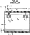
- JP-A-2000-307116 discloses IGBT having a structure in which an arrangement pitch of a trench gate is changed, as illustrated in FIG 23 .
- a feature of the IGBT in FIG. 23 is that a floating p-layer 105 is formed on a portion where the interval between the trench gates is wide, without forming a p-channel layer 106.
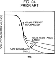
- FIG 24 represents a simulated waveforms of the collector-emitter voltage vce during a turn-on operation. As illustrated in FIG 24 , there is a time period during which the control cannot be performed, that is, dvce/dt does not change even though a gate resistance is changed.
- the accelerated dic/dt cannot be controlled by the outside gate resistance.
- the time period occurs during which dv/dt of the IGBT and the opposite-arm diode cannot be controlled by the gate resistance.
- JP-A-2004-39838 as illustrated in FIG 25 , the floating p-layer 105 is electrically connected to the emitter electrode 114 via a resistor 201, therefore, the electric potential rise at the floating p-layer 105 is inhibited.
- JP-A-5-243561 discloses that a wide trench gate is formed, as illustrated in FIG 26 , to enhance an injection of electrons from the trench gate, and therefore, the loss of the IGBT is reduced.
- JP-A-5-243561 does not explicitly specify, because of no floating p-layer, there is no gate potential variation caused by the effect of the floating p-layer, and therefore, the controllability of the dv/dt can be improved.
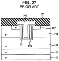
- JP-A-2009-200103 discloses that a gate electrode 301 is formed on a lateral face of the trench and a space between the gate electrodes 301 is filled up with an insulating layer 302, and thereby the parasitic capacitance of a gate insulating layer 110 is reduced, as illustrated in FIG 27 . Therefore, the gate voltage rise can be controlled and the controllability of the dv/dt can be improved.
- the effect of enhancing the injection of electrons becomes small, and thereby, the on-voltage is increased.
- the on-voltage rise becomes small, while there is a problem that the controllability of the dv/dt is reduced.
- An object of the invention is to provide a semiconductor device capable of improving the dv/dt controllability by the gate drive circuit during the turn-on switching time period, while maintaining the low loss and high breakdown voltage, and to provide a power conversion apparatus using the same.
- a semiconductor device of the invention comprises the elements defined in present claim 1.
- the device comprises: a first semiconductor layer of a first conductive type; a second semiconductor layer of a second conductive type formed in the vicinity of a surface of the first semiconductor layer; a third semiconductor layer of the second conductive type adjacent to the first semiconductor layer and formed in the vicinity of a surface of an opposite side of the second semiconductor layer; a fourth semiconductor layer of the first conductive type selectively formed on the third semiconductor layer; a trench penetrating through the fourth semiconductor layer and the third semiconductor layer into the first semiconductor layer; a gate insulating layer formed along an internal face of the trench; an insulating layer formed in the trench; a first conductive layer formed on a surface of the gate insulating layer; and a second conductive layer formed on a surface of the insulating layer, characterized in that the first conductive layer in the trench of at least one cross-sectional structure is divided by the insulating layer and the second conductive layer, a width "a" of the trench is wider than a width "b" of an area in which the trench is not formed
- a power conversion apparatus of the invention comprises: a pair of input terminals; a plurality of series connected circuits, connected between the input terminals, to which a plurality of semiconductor switching devices are connected in series; a plurality of output terminals each connected to a series connected point of each of the plurality of series connected circuits, and the plurality of semiconductor switching devices that turn on and off to perform a power conversion, characterized in that the plurality of semiconductor switching devices are above-mentioned semiconductor devices.
- the semiconductor device and the power conversion apparatus using the same in the invention have an effect that the reverse transfer capacitance can be reduced, and thereby, the dv/dt controllability by the gate drive circuit during the turn-on switching time period can be improved, while maintaining the low loss and high breakdown voltage.
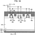
- FIG. 1 shows a cross-sectional structure of an IGBT in a first example useful to understand the semiconductor device of the invention.
- the IGBT illustrated in FIG. 1 is configured by: an n - drift layer 104 as a first semiconductor layer of a first conductive type; a p-collector layer 102 as a second semiconductor layer of a second conductive type formed in the vicinity of the surface of n - drift layer 104, and the layer 102 is contacted to a collector electrode 100; a p-channel layer 106 as a third semiconductor layer of the second conductive type adjacent to the n - drift layer 104 and formed in the vicinity of the surface of a reverse side of the layer 104 with respect to the side of p-collector layer 102; an n-emitter layer 107 as a fourth semiconductor layer of the first conductive type formed selectively on the p-channel layer 106; a trench 423 penetrating the n-emitter layer 107 and the p-channel layer 106 into the n - drift layer 104; a gate insulating layer 402 formed along an internal face of the trench 423; an insulating
- the IGBT of this example has the cross-sectional structure in which the gate electrode 401 is divided by the insulating layer 403 and the emitter electrode 404 in the trench 423, as illustrated in FIG 1 . Further, a width "a" of the trench 423 is wider than a width "b" of an area in which the trench is not formed. A relation, a > b, is satisfied in FIG. 1 , and the gate electrode 401 is formed on the lateral face of wide trench 423.
- the gate electrode 401 is covered by the gate insulating layer 402 and the thick insulating layer 403 (for example, the gate insulating layer 402 is as thick as 100 nm, and the insulating layer (inter layer) 403 is as thick as 1000 nm), a parasitic capacitance of the gate can be drastically reduced, compared with the conventional IGBT illustrated in FIG 23 .
- the conventional IGBT both sides of the gate are covered by a thin gate insulating layer.
- one side is covered by the gate insulating layer 402 and the other side is covered by the thick insulating layer 403, so that the parasitic capacitance of the thick inter layer side is reduced.
- a displacement current is given by (parasitic capacitance) ⁇ (potential variation of floating p-layer), that is, the smaller the parasitic capacitance, the smaller the displacement current. Therefore, the controllability of the dv/dt can be improved,because the potential rise in the gate is controllable due to the reduced displacement current.
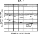
- FIG. 2 represents a simulated result of a collector voltage dependency of a reverse transfer capacitance for the IGBT in this example and the conventional IGBT.
- the parasitic capacitance of the gate is a reverse transfer capacitance component of the IGBT, so that the reverse transfer capacitance is reduced if the parasitic capacitance is reduced.
- the reverse transfer capacitance is reduced up to approximately 1/4 in comparison with the conventional IGBT.
- the IGBT in the first example does not form the floating p-layer which has been formed in the conventional IGBT, therefore, there is no gate potential variation caused by an effect of the floating p-layer and the controllability of the dv/dt can be improved.
- a reduction of the breakdown voltage and the reliability is concerned about because the floating p-layer is not formed.
- the emitter electrode 404 is formed to protrude in the trench to the n - drift layer 104 (the gate electrode 401 is divided by the emitter electrode 404 and the insulating layer 403), therefore, the reduction of the breakdown voltage and reliability can be prevented, because the emitter electrode 404 acts as a field plate which relaxes the electric field applied to a corner portion of the gate electrode 401.
- FIG 3 illustrates simulated waveforms of the collector - emitter voltage, vce, on the turn-on operation of the IGBT according to the first example.
- dvce/dt can be controlled by varying a gate resistance, unlike the case of the conventional IGBT illustrated in FIG 24 .
- FIG 4 illustrate an example of a manufacturing process of the IGBT according to the first example.
- a pattern as illustrated in (b) is formed on the n - drift layer 104 illustrated in (a) using a photoresist 501, and the wide trench 423 is formed by an anisotropic etching as illustrated in (c).
- the gate insulating layer 402 is formed as illustrated in (d), and polysilicon as a material of the gate electrode 401 is deposited, as illustrated in (e), to then be etched back by the anisotropic etching and form the gate electrode 401 made up of the polysilicon on the lateral face of the trench 423 as a sidewall, as illustrated in (f).
- a pattern is formed using a photoresist 502 as illustrated in (g), and an ion implantation of p-type and n-type is performed to form the p-channel layer 106 and n-emitter layer 107 as illustrated in (h).
- the insulating layer 403 is deposited as illustrated in (i)
- a contact hole formed and the p-contact layer 108 is formed as illustrated in (j).
- the emitter electrode 404, the n-buffer layer 103, the p-collector layer 102 and the collector electrode 100 are formed, as illustrated in (k), and thus the process is completed.
- the collector terminal 101 and the p-collector layer 102 on the reverse face are formed after the surface process, however, an epitaxial-substrate on which the p-collector layer 102 are initially formed may be used.
- the gate electrode 401 is formed on the lateral face of the wide trench 423 in the IGBT in the first example, so that the parasitic capacitance of the gate is reduced, and the dv/dt controllability by the gate drive circuit during the turn-on switching time period can be improved.
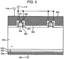
- FIG. 5 illustrates a cross-sectional structure of an IGBT according to an embodiment of the invention.
- a feature of the IGBT in the embodiment is that an insulating layer 403 is thinner than the thickness of the insulating layer 407 (refer to FIG 6 ) in a termination area (not shown, peripheral area of chip), and thereby enhance the field plate effect caused by the emitter electrode 404 and a higher breakdown voltage can be realized.
- the corner portion (corner portion close to the emitter electrode 404 and on the lower side of the gate electrode 401) of the gate electrode 401 and an end portion (corner portion mostly close to the gate electrode 401) of the emitter electrode 404 become closer with each other, the field plate effect becomes higher. In consequence, the high breakdown voltage of the IGBT can be obtained.
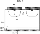
- the termination area of the IGBT made up of a p-layer 405 and a floating electrode 406 as illustrated in FIG 6 if the insulating layer 407 becomes thin (similar extent to the insulating layer 403 as illustrated in FIG 5 ), the electric field in the insulating layer 407 becomes high and thereby reduces the breakdown voltage in the termination area.
- the insulating layer 403 in an active area (area in FIG 5 ) of the IGBT is thinner than the thickness of the insulating layer 407 in the termination area. In consequence, there is an advantage that both the active area and the termination area can maintain the high breakdown voltage.
- the breakdown voltage of the active area is improved by using the thin insulating layer 403, while the breakdown voltage of the termination area is improved by using the thick insulating layer 407. Therefore, the feature of this embodiment is that the thickness of the insulating layer in the two areas is changed.
- the thickness of the insulating layer 403 ranges from 300 nm to 1000 nm and the thickness of insulating layer 407 is equal to or greater than 1000 nm.
- the breakdown voltage continues to improve in the range from 300 nm to 1000 nm in thickness of the oxide layer (insulating layer 403) and is saturated at an equal to or less than 300 nm in thickness.
- the oxide layer is too thin, impurities diffuse up to an Si-layer under the insulating layer when implanting ions. Therefore, the extent of around 300 nm is desirable.
- FIG. 7 illustrates a cross-sectional structure of an IGBT according to a second example useful to understand the invention.
- a feature of the IGBT in the second example is that a trench 424 has a two step staircase pattern, and the n - drift layer 104 side of the emitter electrode 404 protrudes deeper than the corner portion of the gate electrode 401.
- the electric field applied to the corner portion of the gate electrode 401 is dispersed by the n - drift layer 104 side of the emitter electrode 404 and the corner portion of the trench 424, so that a higher breakdown voltage can be obtained from the same reason as described in the embodiment.
- FIG. 8 to FIG. 10 illustrate a cross-sectional structure of an IGBT according to a third example useful to understand the invention.
- a feature of the IGBT in the third example is that a p-layer is inserted underneath the trench 423 to thereby allow a depletion layer to extend from the p-layer. Therefore, the electric fields at the corner portion of the gate electrode 401 and a trench corner portion are relaxed, so that a higher breakdown voltage can be obtained.
- a p-layer 408 is partly inserted underneath trench 423.
- a p-layer 409 is inserted so as to cover the corner portion of the gate electrode 401.
- an n-layer 410 is inserted into the p-layer 409.
- the n-layer 410 in FIG. 10 prevents holes from flowing into the floating p-layer 409 during the turn-on operation. In fact, since less holes flow into the n-layer by forming the n-layer inside the p-layer, the holes to flow into the floating layer are reduced. In consequence, there is an advantage that the potential rise in the floating p-layer is inhibited.
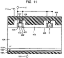
- FIG. 11 to FIG. 13 illustrate a cross-sectional structure of an IGBT according to a fourth example useful to understand the invention.
- a feature of the IGBT in the fourth example is that a p-layer 418 is formed underneath the p-channel layer 106. In consequence, the electric field at the corner of gate electrode 401 is relaxed, so that a higher breakdown voltage can be obtained.
- FIG. 11 it is configured that the p-layer 418 is inserted underneath the p-channel layer.
- a p-layer 419 is inserted so as to cover the corner portion of the gate electrodes 401.
- a p-layers 420 are inserted so as to cover each one of the corner of the gate electrode 401.
- FIG. 14 is a cross-sectional structure of an IGBT according to a fifth example of the invention.
- a feature of the IGBT in the fifth example is that a capacitor made up of an insulating layer 426 and a polysilicon electrode 411 is formed on the trench 423.
- the polysilicon electrode 411 is connected to the emitter electrode 404. Since a part of hole current flowing underneath the trench 423 during the turn-on is used for charging up the capacitor, the potential rise underneath the trench 423 is inhibited. In consequence, there is an advantage that the gate potential rise can be reduced. Since the polysilicon electrode 411 acts as the field plate to relax the electric field at the corner portion of the gate electrode 401, there is also the advantage that the high breakdown voltage can be obtained.
- FIG. 15 to FIG. 19 illustrate a cross-sectional structure of an IGBT according to a sixth example useful to understand the invention.
- a polysilicon electrode 412 is formed on the lateral face of a trench 425 likewise to the gate electrode 401, and the capacitor made up of the gate insulating layer 402 and the polysilicon electrode 412 is connected to the emitter electrode 404.
- the gate potential rise can be reduced during the turn-on operation.
- a p-layer 413 is formed between the polysilicon electrodes 412 to relax the electric field applied to the corner portion of the polysilicon electrode 412, therefore, the high breakdown voltage can be obtained.
- an n-layer 414 is formed on the p-layer 413 to prevent the holes from flowing into the floating p-layer 413 during the turn-on operation. In consequence, there is an advantage that the potential rise of the floating p-layer is inhibited.
- a p-layer 415 is formed so as to cover the corner portion of polysilicon electrode 412, so that a high breakdown voltage can be obtained.
- an n-layer 416 is formed on the p-layer 415 to prevent the holes from flowing into the floating p-type 415 during the turn-on operation, and there is the advantage that the potential rise of the floating p-layer is inhibited.
- FIG. 20 illustrates a cross-sectional structure of an IGBT according to a seventh example useful to understand the invention.
- a feature of the seventh example is that an n-layer 421 is inserted underneath the p-channel layer 106. Since the n-layer 421 works as a barrier for the holes flowing into the emitter electrode 404, a hole concentration in the vicinity of the emitter increases. In consequence, the on-voltage can be further reduced.
- FIG. 21 illustrates a cross-sectional structure of an IGBT according to an eighth example useful to understand the invention.
- a feature of the eighth example is that a p-layer 422 is inserted underneath the n-layer 421.
- the electric field intensity becomes strong at the n-layer 421 during off-state, and it is therefore expected that the breakdown voltage is reduced.
- the p-layer 422 is added to underneath the n-layer 421 to relax the electric field intensity at the n-layer 421. Therefore, the breakdown voltage can be maintained even if the carrier concentration is made high, so that the on-voltage can be further reduced.
- FIG. 22 is a circuit diagram representing a power conversion apparatus employing the IGBT described in the above-mentioned embodiments.and examples.
- FIG. 22 represents an inverter circuit diagram in the embodiments and examples.
- a reference numeral 601 denotes a gate drive circuit
- 602 denotes an IGBT
- 603 denotes a diode
- 604, 605 denote an input terminal
- 606 to 608 denote an output terminal.
- a power conversion apparatus is configured in which the IGBT described in the first to eight examples and/or the embodiment is applied to the inverter circuit.
- the IGBT in the embodiments and examples mentioned above is applied to the power conversion apparatus to thereby realize a low loss and high reliability of the power conversion apparatus.
Landscapes
- Electrodes Of Semiconductors (AREA)
- Metal-Oxide And Bipolar Metal-Oxide Semiconductor Integrated Circuits (AREA)
- Insulated Gate Type Field-Effect Transistor (AREA)
Description
- The present invention relates to a semiconductor device which is an insulated gate bipolar transistor (hereinafter abbreviated to IGBT) having an insulated trench gate structure and a power conversion apparatus using the same.
- The IGBT is a switching device for controlling a current to be flown between a collector electrode and an emitter electrode in response to a voltage applied to a gate electrode. Since electric power to be controlled by IGBT is ranged from several tens to several hundred thousand watts and switching frequency is ranging from several tens to over hundred kilohertz, the IGBT has been widely used from low electric power devices, such as an air-conditioner, microwave oven, etc. for household use to high electric power devices, such as an inverter for use in railroad rolling stock, steel plant, etc.
- For the purpose of realizing a high efficiency operation of the electric devices, IGBT has been demanded for a low loss, that is, demanded for reduction of a conduction loss and a switching loss. At the same time, it has been demanded that dv/dt can be controlled to fit a specification for an application so as to prevent a problem, such as EMC noise, malfunction, breakdown of motors, etc.
- Incidentally,
JP-A-2000-307116 FIG 23 . A feature of the IGBT inFIG. 23 is that a floating p-layer 105 is formed on a portion where the interval between the trench gates is wide, without forming a p-channel layer 106. - In the configuration as mentioned above, since a current is only flown into a portion where the interval between the trench gates is narrower, an over current flowing at a short circuit can be inhibited, therefore, a ruggedness of the device can be improved. Further, since a part of a hole current flows into an
emitter electrode 114 via the floating p-layer 105, a hole concentration increases around theemitter electrode 114, therefore, there is also an advantage that an on-state voltage can be reduced. Furthermore, there is also an advantage that an electric field applied to the trench gate is relaxed by a p-n junction formed of the floating p-layer 105 and an n- drift layer 104.US 2005/263852 A1 discloses a device with the features in the preamble of present claim 1. Other conventional semiconductor devices are shown inUS 2003/160270 A1 ,US 2008/283867 A1 ,US 2004/041171 A1 ,US 2009/114923 A1 , andUS 2005/001264 A1 . - However, in the IGBT illustrated in
FIG 23 , a problem sometimes occurs that controllability of the time change of an output voltage, dv/dt, of the IGBT and opposite-arm diode reduces when the IGBT turns on.FIG 24 represents a simulated waveforms of the collector-emitter voltage vce during a turn-on operation. As illustrated inFIG 24 , there is a time period during which the control cannot be performed, that is, dvce/dt does not change even though a gate resistance is changed. - This reason is considered, as follows. When the IGBT turnes on, holes flow transiently into the floating p-
layer 105 inFIG 23 , and an electric potential at the floating p-layer 105 becomes high. At this time, since a displacement current flows into agate electrode 109 via a parasitic capacitance of agate insulating layer 110 and thereby a gate voltage is raised, a time change of a collector current, dic/dt, determined by the product of a mutual conductance, gm, in a MOSFET structure and a time change of a voltage between the gate and emitter, dvge/dt, increases, and thereby, a switching speed is accelerated. The amount of holes transiently flown into the floating p-layer 105 is determined mainly by the structure inside the semiconductor. Therefore, it is difficult to control the amount of holes by an outside gate resistance. - Therefore, the accelerated dic/dt cannot be controlled by the outside gate resistance. As a result, the time period occurs during which dv/dt of the IGBT and the opposite-arm diode cannot be controlled by the gate resistance.
- For the purpose of inhibiting the gate potential rise caused by the effect of the floating p-
layer 105, the following methods have been proposed. - In
JP-A-2004-39838 FIG 25 , the floating p-layer 105 is electrically connected to theemitter electrode 114 via aresistor 201, therefore, the electric potential rise at the floating p-layer 105 is inhibited. - In this way, the displacement current flowing into the
gate electrode 109 from the floating p-layer 105 decreases, and therefore, inhibits the gate potential rise. As a result of this, the controllability of the dv/dt of the IGBT and the opposite-arm diode can be improved. -
JP-A-5-243561 FIG 26 , to enhance an injection of electrons from the trench gate, and therefore, the loss of the IGBT is reduced. AlthoughJP-A-5-243561 -
JP-A-2009-200103 gate electrode 301 is formed on a lateral face of the trench and a space between thegate electrodes 301 is filled up with aninsulating layer 302, and thereby the parasitic capacitance of agate insulating layer 110 is reduced, as illustrated inFIG 27 . Therefore, the gate voltage rise can be controlled and the controllability of the dv/dt can be improved. - A document "Y. Onozawa, et al., Proc. 19th ISPSD, pp13-16, 2007" discloses that, as illustrated in
FIG. 28 ,a p base layer 106 electrically connected with the emitter electrode is alternately disposed toward a direction in parallel with the trench at every cell without using the floating p-layer. Therefore, there is no gate potential variation caused by the effect of the floating p-layer and the controllability of the dv/dt can be improved because the floating p-layer is not used. - Incidentally, it has been demanded that the dv/dt controllability by the gate drive circuit during a turn-on switching time period is improved while maintaining the low loss and high breakdown voltage in IGBT. For this problem, it was appreciated that the structure in the documents as mentioned above has the following improvement points.
- In the
JP-A-2004-39838 resistor 201 between thefloating p layer 105 andemitter electrode 114 becomes, the more the controllability of the dv/dt is improved. However, since a part of the hole current at on-state flows out to theemitter electrode 114 via theresistor 201, the effect of enhancing the injection of electrons becomes small, and thereby, the on-voltage is increased. Conversely, when increasing the resistance value ofresistor 201, the on-voltage rise becomes small, while there is a problem that the controllability of the dv/dt is reduced. - In the
JP-A-5-243561 - In the
JP-A-2009-200103 gate electrode 301 formed on a lateral face is increased. - In the document "Y. Onozawa, et al., Proc. 19the ISPSD, pp13-16 2007", there is a problem that the electric field applied to the
gate electrode 109 increases and thereby the breakdown voltage and reliability is reduced, because thep base layers 106 are partially removed. - The present invention is made in light of the above-mentioned points. An object of the invention is to provide a semiconductor device capable of improving the dv/dt controllability by the gate drive circuit during the turn-on switching time period, while maintaining the low loss and high breakdown voltage, and to provide a power conversion apparatus using the same. In order to achieve the above-mentioned object, a semiconductor device of the invention comprises the elements defined in present claim 1.
- According to an example, the device comprises: a first semiconductor layer of a first conductive type; a second semiconductor layer of a second conductive type formed in the vicinity of a surface of the first semiconductor layer; a third semiconductor layer of the second conductive type adjacent to the first semiconductor layer and formed in the vicinity of a surface of an opposite side of the second semiconductor layer; a fourth semiconductor layer of the first conductive type selectively formed on the third semiconductor layer; a trench penetrating through the fourth semiconductor layer and the third semiconductor layer into the first semiconductor layer; a gate insulating layer formed along an internal face of the trench; an insulating layer formed in the trench; a first conductive layer formed on a surface of the gate insulating layer; and a second conductive layer formed on a surface of the insulating layer, characterized in that the first conductive layer in the trench of at least one cross-sectional structure is divided by the insulating layer and the second conductive layer, a width "a" of the trench is wider than a width "b" of an area in which the trench is not formed, and the first conductive layer and the gate insulating layer are formed on a lateral face of the trench.
- Further, a power conversion apparatus of the invention comprises: a pair of input terminals; a plurality of series connected circuits, connected between the input terminals, to which a plurality of semiconductor switching devices are connected in series; a plurality of output terminals each connected to a series connected point of each of the plurality of series connected circuits, and the plurality of semiconductor switching devices that turn on and off to perform a power conversion, characterized in that the plurality of semiconductor switching devices are above-mentioned semiconductor devices.
- The semiconductor device and the power conversion apparatus using the same in the invention have an effect that the reverse transfer capacitance can be reduced, and thereby, the dv/dt controllability by the gate drive circuit during the turn-on switching time period can be improved, while maintaining the low loss and high breakdown voltage.
- The other objects, aspects and advantages of the invention will become apparent from the following description of the embodiments of the invention taken in conjunction with the accompanying drawings.
-
-
FIG. 1 is a cross-section diagram illustrating an IGBT as a semiconductor device according to a first example useful to understand the invention; -
FIG. 2 is a simulated characteristic diagram representing a collector voltage dependency of the reverse transfer capacitances of the IGBT according to the first example and in theJP-A-2000-307116 -
FIG. 3 is a characteristic diagram illustrating the simulated waveforms of collector - emitter voltage during the turn-on operation of an IGBT according to the first example; -
FIG. 4 is a diagram illustrating a manufacturing process of an IGBT according to the first example; -
FIG 5 is a cross-section diagram illustrating an IGBT according to an embodiment of the semiconductor device of the invention; -
FIG 6 is a cross-section diagram of a termination area of an IGBT according to the embodiment; -
FIG 7 is a cross-section diagram illustrating an IGBT according to a second example useful to understand the semiconductor device of the invention; -
FIG 8 is a cross-section diagram illustrating an IGBT according to a third example useful to understand the semiconductor device of the invention; -
FIG. 9 is a cross-section diagram illustrating an IGBT according to an example of the third example; -
FIG. 10 is a cross-section diagram illustrating an IGBT according to an other example of the third example; -
FIG 11 is a cross-section diagram illustrating an IGBT according to a fourth example useful to understand the semiconductor device of the invention; -
FIG. 12 is a cross-section diagram illustrating an IGBT according to an example of the fourth example; -
FIG. 13 is a cross-section diagram illustrating an IGBT according to an other example of the fourth example; -
FIG. 14 is a cross-section diagram illustrating an IGBT according to a fifth example useful to understand the semiconductor device of the invention; -
FIG 15 is a cross-section diagram illustrating an IGBT according to a sixth example useful to understand the semiconductor device of the invention; -
FIG. 16 is a cross-section diagram illustrating an IGBT according to an example of the sixth example; -
FIG. 17 is a cross-section diagram illustrating an IGBT according to an other example of the sixth example; -
FIG. 18 is a cross-section diagram illustrating an IGBT according to an other example of the sixth example; -
FIG. 19 is a cross-section diagram illustrating an IGBT according to an other example of the sixth example. -
FIG 20 is a cross-section diagram illustrating an IGBT according to a seventh example useful to understand the semiconductor device of the invention; -
FIG 21 is a cross-section diagram illustrating an IGBT according to an eight example useful to understand the semiconductor device of the invention; -
FIG. 22 is a circuit diagram representing one embodiment of a power conversion apparatus of the invention; -
FIG 23 is a cross-section diagram illustrating a conventional IGBT disclosed in theJP-A-2000-307116 -
FIG 24 is a characteristic diagram illustrating a simulated waveforms of the collector- emitter voltage during the turn-on operation of the conventional IGBT disclosed in theJP-A-2000-307116 -
FIG 25 is a cross-section diagram illustrating the conventional IGBT disclosed in theJP-A-2004-39838 -
FIG 26 is a cross-section diagram illustrating the conventional IGBT disclosed in theJP-A-5-243561 -
FIG 27 is a cross-section diagram illustrating the conventional IGBT disclosed in theJP-A-2009-200103 -
FIG 28 is a perspective diagram illustrating a partly broken portion of the conventional IGBT disclosed in the document "Y. Onozawa, et al., Proc. 19th ISPSD, pp13-16 2007"; and -
FIG. 29 is a characteristic diagram for explaining grounds of a thickness of the insulating layer in the second example. - Hereinafter, a semiconductor device will be described in detail with reference to illustrated embodiments and examples.
-
FIG. 1 shows a cross-sectional structure of an IGBT in a first example useful to understand the semiconductor device of the invention. - The IGBT illustrated in
FIG. 1 is configured by: an n- drift layer 104 as a first semiconductor layer of a first conductive type; a p-collector layer 102 as a second semiconductor layer of a second conductive type formed in the vicinity of the surface of n- drift layer 104, and the layer 102 is contacted to a collector electrode 100; a p-channel layer 106 as a third semiconductor layer of the second conductive type adjacent to the n- drift layer 104 and formed in the vicinity of the surface of a reverse side of the layer 104 with respect to the side of p-collector layer 102; an n-emitter layer 107 as a fourth semiconductor layer of the first conductive type formed selectively on the p-channel layer 106; a trench 423 penetrating the n-emitter layer 107 and the p-channel layer 106 into the n- drift layer 104; a gate insulating layer 402 formed along an internal face of the trench 423; an insulating layer 403 formed in the trench 423; a gate electrode 401 as a first conductive layer formed on the surface of the gate insulating layer 402; an emitter electrode 404 as the second conductive layer formed on the surface of the insulating layer 403 and protruding partly in the trench 423 to the side of the n- drift layer 104; an n-buffer layer 103 formed between the p-collector layer 102 and the n- drift layer 104; and a p-contact layer 108 formed in the p-channel layer 106. In addition, areference numeral 101 denotes a collector terminal, 115 denotes a gate terminal, and 116 denotes an emitter terminal. - The IGBT of this example has the cross-sectional structure in which the
gate electrode 401 is divided by the insulatinglayer 403 and theemitter electrode 404 in thetrench 423, as illustrated inFIG 1 . Further, a width "a" of thetrench 423 is wider than a width "b" of an area in which the trench is not formed. A relation, a > b, is satisfied inFIG. 1 , and thegate electrode 401 is formed on the lateral face ofwide trench 423. Since thegate electrode 401 is covered by thegate insulating layer 402 and the thick insulating layer 403 (for example, thegate insulating layer 402 is as thick as 100 nm, and the insulating layer (inter layer) 403 is as thick as 1000 nm), a parasitic capacitance of the gate can be drastically reduced, compared with the conventional IGBT illustrated inFIG 23 . In the conventional IGBT, both sides of the gate are covered by a thin gate insulating layer. In contrast, in the structure of this example, one side is covered by thegate insulating layer 402 and the other side is covered by the thick insulatinglayer 403, so that the parasitic capacitance of the thick inter layer side is reduced. A displacement current is given by (parasitic capacitance) × (potential variation of floating p-layer), that is, the smaller the parasitic capacitance, the smaller the displacement current. Therefore, the controllability of the dv/dt can be improved,because the potential rise in the gate is controllable due to the reduced displacement current. -
FIG. 2 represents a simulated result of a collector voltage dependency of a reverse transfer capacitance for the IGBT in this example and the conventional IGBT. The parasitic capacitance of the gate is a reverse transfer capacitance component of the IGBT, so that the reverse transfer capacitance is reduced if the parasitic capacitance is reduced. As is apparent fromFIG 2 , in the IGBT of the first example, the reverse transfer capacitance is reduced up to approximately 1/4 in comparison with the conventional IGBT. - Further, the IGBT in the first example does not form the floating p-layer which has been formed in the conventional IGBT, therefore, there is no gate potential variation caused by an effect of the floating p-layer and the controllability of the dv/dt can be improved. A reduction of the breakdown voltage and the reliability is concerned about because the floating p-layer is not formed. However, the
emitter electrode 404 is formed to protrude in the trench to the n- drift layer 104 (thegate electrode 401 is divided by theemitter electrode 404 and the insulating layer 403), therefore, the reduction of the breakdown voltage and reliability can be prevented, because theemitter electrode 404 acts as a field plate which relaxes the electric field applied to a corner portion of thegate electrode 401. -
FIG 3 illustrates simulated waveforms of the collector - emitter voltage, vce, on the turn-on operation of the IGBT according to the first example. As is apparent fromFIG 3 , in the IGBT of the first example, it is appreciated that dvce/dt can be controlled by varying a gate resistance, unlike the case of the conventional IGBT illustrated inFIG 24 . - In
FIG 4 , (a) to (k) illustrate an example of a manufacturing process of the IGBT according to the first example. First, a pattern as illustrated in (b) is formed on the n- drift layer 104 illustrated in (a) using aphotoresist 501, and thewide trench 423 is formed by an anisotropic etching as illustrated in (c). Next, thegate insulating layer 402 is formed as illustrated in (d), and polysilicon as a material of thegate electrode 401 is deposited, as illustrated in (e), to then be etched back by the anisotropic etching and form thegate electrode 401 made up of the polysilicon on the lateral face of thetrench 423 as a sidewall, as illustrated in (f). Next, a pattern is formed using aphotoresist 502 as illustrated in (g), and an ion implantation of p-type and n-type is performed to form the p-channel layer 106 and n-emitter layer 107 as illustrated in (h). Subsequently, the insulatinglayer 403 is deposited as illustrated in (i), a contact hole formed and the p-contact layer 108 is formed as illustrated in (j). Finally, theemitter electrode 404, the n-buffer layer 103, the p-collector layer 102 and thecollector electrode 100 are formed, as illustrated in (k), and thus the process is completed. - In this example, the
collector terminal 101 and the p-collector layer 102 on the reverse face are formed after the surface process, however, an epitaxial-substrate on which the p-collector layer 102 are initially formed may be used. - As mentioned above, the
gate electrode 401 is formed on the lateral face of thewide trench 423 in the IGBT in the first example, so that the parasitic capacitance of the gate is reduced, and the dv/dt controllability by the gate drive circuit during the turn-on switching time period can be improved. -
FIG. 5 illustrates a cross-sectional structure of an IGBT according to an embodiment of the invention. A feature of the IGBT in the embodiment is that an insulatinglayer 403 is thinner than the thickness of the insulating layer 407 (refer toFIG 6 ) in a termination area (not shown, peripheral area of chip), and thereby enhance the field plate effect caused by theemitter electrode 404 and a higher breakdown voltage can be realized. As illustrated inFIG. 5 , as the corner portion (corner portion close to theemitter electrode 404 and on the lower side of the gate electrode 401) of thegate electrode 401 and an end portion (corner portion mostly close to the gate electrode 401) of theemitter electrode 404 become closer with each other, the field plate effect becomes higher. In consequence, the high breakdown voltage of the IGBT can be obtained. - However, in the termination area of the IGBT made up of a p-
layer 405 and a floatingelectrode 406 as illustrated inFIG 6 , if the insulatinglayer 407 becomes thin (similar extent to the insulatinglayer 403 as illustrated inFIG 5 ), the electric field in the insulatinglayer 407 becomes high and thereby reduces the breakdown voltage in the termination area. In the embodiment, the insulatinglayer 403 in an active area (area inFIG 5 ) of the IGBT is thinner than the thickness of the insulatinglayer 407 in the termination area. In consequence, there is an advantage that both the active area and the termination area can maintain the high breakdown voltage. That is, the breakdown voltage of the active area is improved by using the thin insulatinglayer 403, while the breakdown voltage of the termination area is improved by using the thick insulatinglayer 407. Therefore, the feature of this embodiment is that the thickness of the insulating layer in the two areas is changed. - Specifically, the thickness of the insulating
layer 403 ranges from 300 nm to 1000 nm and the thickness of insulatinglayer 407 is equal to or greater than 1000 nm. As illustrated inFIG 29 , the breakdown voltage continues to improve in the range from 300 nm to 1000 nm in thickness of the oxide layer (insulating layer 403) and is saturated at an equal to or less than 300 nm in thickness. Further, if the oxide layer is too thin, impurities diffuse up to an Si-layer under the insulating layer when implanting ions. Therefore, the extent of around 300 nm is desirable. -
FIG. 7 illustrates a cross-sectional structure of an IGBT according to a second example useful to understand the invention. A feature of the IGBT in the second example is that atrench 424 has a two step staircase pattern, and the n- drift layer 104 side of theemitter electrode 404 protrudes deeper than the corner portion of thegate electrode 401. - By forming the structure as in the second example as mentioned above, the electric field applied to the corner portion of the
gate electrode 401 is dispersed by the n- drift layer 104 side of theemitter electrode 404 and the corner portion of thetrench 424, so that a higher breakdown voltage can be obtained from the same reason as described in the embodiment. -
FIG. 8 to FIG. 10 illustrate a cross-sectional structure of an IGBT according to a third example useful to understand the invention. A feature of the IGBT in the third example is that a p-layer is inserted underneath thetrench 423 to thereby allow a depletion layer to extend from the p-layer. Therefore, the electric fields at the corner portion of thegate electrode 401 and a trench corner portion are relaxed, so that a higher breakdown voltage can be obtained. InFIG 8 , a p-layer 408 is partly inserted underneathtrench 423. InFIG 9 , a p-layer 409 is inserted so as to cover the corner portion of thegate electrode 401. InFIG 10 , an n-layer 410 is inserted into the p-layer 409. The n-layer 410 inFIG. 10 prevents holes from flowing into the floating p-layer 409 during the turn-on operation. In fact, since less holes flow into the n-layer by forming the n-layer inside the p-layer, the holes to flow into the floating layer are reduced. In consequence, there is an advantage that the potential rise in the floating p-layer is inhibited. -
FIG. 11 to FIG. 13 illustrate a cross-sectional structure of an IGBT according to a fourth example useful to understand the invention. A feature of the IGBT in the fourth example is that a p-layer 418 is formed underneath the p-channel layer 106. In consequence, the electric field at the corner ofgate electrode 401 is relaxed, so that a higher breakdown voltage can be obtained. InFIG. 11 , it is configured that the p-layer 418 is inserted underneath the p-channel layer. InFIG 12 , a p-layer 419 is inserted so as to cover the corner portion of thegate electrodes 401. InFIG. 13 , a p-layers 420 are inserted so as to cover each one of the corner of thegate electrode 401. -
FIG. 14 is a cross-sectional structure of an IGBT according to a fifth example of the invention. A feature of the IGBT in the fifth example is that a capacitor made up of an insulatinglayer 426 and apolysilicon electrode 411 is formed on thetrench 423. Thepolysilicon electrode 411 is connected to theemitter electrode 404. Since a part of hole current flowing underneath thetrench 423 during the turn-on is used for charging up the capacitor, the potential rise underneath thetrench 423 is inhibited. In consequence, there is an advantage that the gate potential rise can be reduced. Since thepolysilicon electrode 411 acts as the field plate to relax the electric field at the corner portion of thegate electrode 401, there is also the advantage that the high breakdown voltage can be obtained. -
FIG. 15 to FIG. 19 illustrate a cross-sectional structure of an IGBT according to a sixth example useful to understand the invention. InFIG. 15 , apolysilicon electrode 412 is formed on the lateral face of atrench 425 likewise to thegate electrode 401, and the capacitor made up of thegate insulating layer 402 and thepolysilicon electrode 412 is connected to theemitter electrode 404. In consequence, there is an advantage that the gate potential rise can be reduced during the turn-on operation. InFIG 16 , a p-layer 413 is formed between thepolysilicon electrodes 412 to relax the electric field applied to the corner portion of thepolysilicon electrode 412, therefore, the high breakdown voltage can be obtained. InFIG 17 , an n-layer 414 is formed on the p-layer 413 to prevent the holes from flowing into the floating p-layer 413 during the turn-on operation. In consequence, there is an advantage that the potential rise of the floating p-layer is inhibited. InFIG 18 , a p-layer 415 is formed so as to cover the corner portion ofpolysilicon electrode 412, so that a high breakdown voltage can be obtained. Further, inFIG. 19 , an n-layer 416 is formed on the p-layer 415 to prevent the holes from flowing into the floating p-type 415 during the turn-on operation, and there is the advantage that the potential rise of the floating p-layer is inhibited. -
FIG. 20 illustrates a cross-sectional structure of an IGBT according to a seventh example useful to understand the invention. A feature of the seventh example is that an n-layer 421 is inserted underneath the p-channel layer 106. Since the n-layer 421 works as a barrier for the holes flowing into theemitter electrode 404, a hole concentration in the vicinity of the emitter increases. In consequence, the on-voltage can be further reduced. -
FIG. 21 illustrates a cross-sectional structure of an IGBT according to an eighth example useful to understand the invention. A feature of the eighth example is that a p-layer 422 is inserted underneath the n-layer 421. In the structure of the seventh example, the higher the carrier concentration of the n-layer 421, the higher the barrier for the holes, so that the reduction effect of the on-voltage becomes high. However, the electric field intensity becomes strong at the n-layer 421 during off-state, and it is therefore expected that the breakdown voltage is reduced. - In this example as mentioned above, the p-
layer 422 is added to underneath the n-layer 421 to relax the electric field intensity at the n-layer 421. Therefore, the breakdown voltage can be maintained even if the carrier concentration is made high, so that the on-voltage can be further reduced. -
FIG. 22 is a circuit diagram representing a power conversion apparatus employing the IGBT described in the above-mentioned embodiments.and examples. -
FIG. 22 represents an inverter circuit diagram in the embodiments and examples. Areference numeral 601 denotes a gate drive circuit, 602 denotes an IGBT, 603 denotes a diode, 604, 605 denote an input terminal, and 606 to 608 denote an output terminal. A power conversion apparatus is configured in which the IGBT described in the first to eight examples and/or the embodiment is applied to the inverter circuit. - The IGBT in the embodiments and examples mentioned above is applied to the power conversion apparatus to thereby realize a low loss and high reliability of the power conversion apparatus.
- The same advantages as in the inverters described above can also be obtained in a power conversion apparatus such as a converter, chopper, etc.
- It should be further understood by those skilled in the art that although the foregoing description has been made on embodiments of the invention, the invention is not limited thereto and various changes and modifications may be made without departing from the scope of the appended claims.
Claims (8)
- A semiconductor device, which is an insulated gate bipolar transistor, comprising:a first semiconductor layer (104) of a first conductive type;a second semiconductor layer (102) of a second conductive type formed in the vicinity of a surface first semiconductor layer (104);a third semiconductor layer (106) of the second conductive type adjacent to the first semiconductor layer (104) and formed in the vicinity of a surface of an opposite side of the second semiconductor layer (102);a fourth semiconductor layer (107) first conductive type selectively formed on the third semiconductor layer (106);a trench (423) penetrating through the fourth semiconductor layer (107) and the third semiconductor layer (106) into the first semiconductor layer (104);a gate insulating layer (402) formed along an internal face of the trench (423);a first insulating layer (403) formed in contact with the gate insulating layer (402) in the trench (423);a gate electrode (401) formed on a surface of the gate insulating layer (402); andan emitter electrode (404) formed on a surface of the first insulating layer (403),whereinthe gate electrode (401) in the trench (423) of at least one cross-sectional structure is divided by the first insulating layer (403) and the emitter electrode (404),a width "a" of the trench (423) is wider than a width "b" of an area in which the trench (423) is not formed,the first insulating layer (403) is formed in an active area of the semiconductor device,the gate electrode (401) and the gate insulating layer (402) are formed on a lateral face of the trench (423), andone side of the gate electrode (401) is covered by the gate insulating layer (402) and the opposite side of the gate electrode (401) is covered by the first insulating layer (403),characterised in thata third insulating layer (407) is formed on the first semiconductor layer (104) in a termination area of the semiconductor device,the termination area comprises a region (405) of the second conductivity type formed in the surface of the first semiconductor layer (104) and connected to a floating electrode (406) formed on the surface of the third insulating layer (407),the first insulating layer (403) is thinner than the third insulating layer (407), anda thickness of the first insulating layer (403) in the active area of the semiconductor device ranges from 300 nm to 1000 nm.
- The semiconductor device according to claim 1, wherein the first insulating layer (403) is thicker than the gate insulating layer (402).
- The semiconductor device according to any preceding claim, wherein a seventh semiconductor layer (418; 419; 420) of the second conductive type is formed underneath the third semiconductor layer (106).
- The semiconductor device according to claim 3, wherein the seventh semiconductor layer (419) covers at least one part of the first semiconductor layer (104) underneath a corner portion of the gate electrode (401).
- The semiconductor device according to claim 3, wherein the seventh semiconductor layer is divided into two layers (420), and the respective seventh semiconductor layers (420) cover at least one part of the first semiconductor layer (104) underneath a corner portion of the gate electrode (401).
- The semiconductor device according to any preceding claim, wherein a tenth semiconductor layer (421) of the first conductive type is formed underneath the third semiconductor layer (106).
- The semiconductor device according to any preceding claim, wherein an eleventh semiconductor layer (422) of the second conductive type is formed underneath the tenth semiconductor layer (421).
- A power conversion apparatus comprising:a pair of input terminals (604, 605);a plurality of series connected circuits (601, 602, 603), connected between the input terminals (604, 605), in which a plurality of semiconductor switching devices (602, 603) are connected in series;a plurality of output terminals (606, 607, 608) each connected to a series connected point of the plurality of series connected circuits (601, 602, 603),whereinthe plurality of semiconductor switching devices (602, 603) are adapted to turn on and off to perform a power conversion, andeach of the plurality of semiconductor switching devices (602, 603) is the semiconductor device according to any one of claims 1 to 7.
Applications Claiming Priority (1)
| Application Number | Priority Date | Filing Date | Title |
|---|---|---|---|
| JP2009275047A JP5452195B2 (en) | 2009-12-03 | 2009-12-03 | Semiconductor device and power conversion device using the same |
Publications (3)
| Publication Number | Publication Date |
|---|---|
| EP2365531A2 EP2365531A2 (en) | 2011-09-14 |
| EP2365531A3 EP2365531A3 (en) | 2012-04-04 |
| EP2365531B1 true EP2365531B1 (en) | 2020-03-04 |
Family
ID=44081379
Family Applications (1)
| Application Number | Title | Priority Date | Filing Date |
|---|---|---|---|
| EP10015210.7A Active EP2365531B1 (en) | 2009-12-03 | 2010-12-01 | Semiconductor device and power conversion apparatus using the same |
Country Status (4)
| Country | Link |
|---|---|
| US (2) | US8546847B2 (en) |
| EP (1) | EP2365531B1 (en) |
| JP (1) | JP5452195B2 (en) |
| CN (1) | CN102136490B (en) |
Families Citing this family (22)
| Publication number | Priority date | Publication date | Assignee | Title |
|---|---|---|---|---|
| JP5452195B2 (en) * | 2009-12-03 | 2014-03-26 | 株式会社 日立パワーデバイス | Semiconductor device and power conversion device using the same |
| JP5631752B2 (en) | 2011-01-12 | 2014-11-26 | 株式会社 日立パワーデバイス | Semiconductor device and power conversion device |
| WO2013004829A1 (en) * | 2011-07-07 | 2013-01-10 | Abb Technology Ag | Insulated gate bipolar transistor |
| JP5806535B2 (en) | 2011-07-20 | 2015-11-10 | 株式会社 日立パワーデバイス | Semiconductor device and power conversion device using the same |
| US9595602B2 (en) | 2012-09-07 | 2017-03-14 | Hitachi, Ltd. | Switching device for power conversion and power conversion device |
| CN103855205A (en) * | 2012-12-05 | 2014-06-11 | 三垦电气株式会社 | Semiconductor devices and driving method |
| JP5932623B2 (en) * | 2012-12-05 | 2016-06-08 | 株式会社 日立パワーデバイス | Semiconductor device and power conversion device using the same |
| WO2014168171A1 (en) * | 2013-04-11 | 2014-10-16 | 富士電機株式会社 | Semiconductor device and semiconductor device manufacturing method |
| US9843181B2 (en) * | 2013-07-25 | 2017-12-12 | Infineon Technologies Austria Ag | Semiconductor device including a control circuit |
| CN103413761A (en) * | 2013-08-20 | 2013-11-27 | 上海北车永电电子科技有限公司 | Insulated gate bipolar transistor and manufacturing method thereof |
| KR102281459B1 (en) * | 2014-11-05 | 2021-07-27 | 삼성전기주식회사 | Printed circuit board and manufacturing method thereof |
| WO2017114235A1 (en) * | 2015-12-28 | 2017-07-06 | 电子科技大学 | Lateral insulated gate bipolar transistor and method for eliminating transistor tail current |
| JP2017174923A (en) | 2016-03-23 | 2017-09-28 | ルネサスエレクトロニクス株式会社 | Semiconductor device |
| JP6981777B2 (en) * | 2017-05-29 | 2021-12-17 | 株式会社 日立パワーデバイス | Semiconductor device |
| WO2019143733A1 (en) * | 2018-01-16 | 2019-07-25 | Ipower Semiconductor | Self-aligned and robust igbt devices |
| CN109037357A (en) * | 2018-08-06 | 2018-12-18 | 南京方旭智芯微电子科技有限公司 | Low miller capacitance manufacturing method |
| JP6627948B2 (en) * | 2018-10-31 | 2020-01-08 | 富士電機株式会社 | Semiconductor device |
| GB2587645B (en) | 2019-10-03 | 2022-08-03 | Mqsemi Ag | Semiconductor device having a gate electrode formed in a trench structure |
| US20230335625A1 (en) * | 2021-03-31 | 2023-10-19 | Dynex Semiconductor Limited | Power semiconductor device |
| JP7627629B2 (en) * | 2021-06-30 | 2025-02-06 | 株式会社日立製作所 | Silicon carbide semiconductor device and manufacturing method thereof |
| JP7728216B6 (en) | 2022-03-23 | 2025-09-19 | 株式会社東芝 | Semiconductor Devices |
| CN114582965B (en) * | 2022-05-06 | 2022-07-19 | 南京微盟电子有限公司 | A low switching loss power device structure and its manufacturing method |
Citations (1)
| Publication number | Priority date | Publication date | Assignee | Title |
|---|---|---|---|---|
| US20050001264A1 (en) * | 2003-04-23 | 2005-01-06 | Syotaro Ono | Semiconductor device having verical MOS gate structure and method of manufacturing the same |
Family Cites Families (50)
| Publication number | Priority date | Publication date | Assignee | Title |
|---|---|---|---|---|
| DE69233105T2 (en) | 1991-08-08 | 2004-05-06 | Kabushiki Kaisha Toshiba, Kawasaki | Insulated trench gate bipolar transistor |
| JP3307785B2 (en) * | 1994-12-13 | 2002-07-24 | 三菱電機株式会社 | Insulated gate semiconductor device |
| JP3288218B2 (en) | 1995-03-14 | 2002-06-04 | 三菱電機株式会社 | Insulated gate semiconductor device and method of manufacturing the same |
| DE19705276A1 (en) * | 1996-12-06 | 1998-08-20 | Semikron Elektronik Gmbh | IGBT with trench gate structure |
| US6180966B1 (en) * | 1997-03-25 | 2001-01-30 | Hitachi, Ltd. | Trench gate type semiconductor device with current sensing cell |
| JP4310017B2 (en) | 1999-02-17 | 2009-08-05 | 株式会社日立製作所 | Semiconductor device and power conversion device |
| JP4829003B2 (en) | 1999-02-17 | 2011-11-30 | 株式会社日立製作所 | Semiconductor device and power conversion device |
| US6413822B2 (en) * | 1999-04-22 | 2002-07-02 | Advanced Analogic Technologies, Inc. | Super-self-aligned fabrication process of trench-gate DMOS with overlying device layer |
| JP2001237249A (en) * | 2000-02-21 | 2001-08-31 | Hitachi Ltd | Semiconductor device and method of manufacturing the same |
| JP4231612B2 (en) * | 2000-04-26 | 2009-03-04 | 株式会社ルネサステクノロジ | Semiconductor integrated circuit |
| US6635544B2 (en) | 2001-09-07 | 2003-10-21 | Power Intergrations, Inc. | Method of fabricating a high-voltage transistor with a multi-layered extended drain structure |
| WO2003046999A1 (en) * | 2001-11-30 | 2003-06-05 | Shindengen Electric Manufacturing Co., Ltd. | Semiconductor device and manufacturing method thereof |
| DE10203164B4 (en) * | 2002-01-28 | 2005-06-16 | Infineon Technologies Ag | Power semiconductor component and method for its production |
| JP2004022941A (en) * | 2002-06-19 | 2004-01-22 | Toshiba Corp | Semiconductor device |
| JP4676125B2 (en) | 2002-07-03 | 2011-04-27 | ルネサスエレクトロニクス株式会社 | Trench gate type insulated gate bipolar transistor |
| JP3997126B2 (en) * | 2002-08-29 | 2007-10-24 | 株式会社ルネサステクノロジ | Trench gate type semiconductor device |
| JP4028333B2 (en) | 2002-09-02 | 2007-12-26 | 株式会社東芝 | Semiconductor device |
| JP3927111B2 (en) * | 2002-10-31 | 2007-06-06 | 株式会社東芝 | Power semiconductor device |
| JP2004228342A (en) * | 2003-01-23 | 2004-08-12 | Denso Corp | Semiconductor device and method of manufacturing the same |
| JP4483179B2 (en) * | 2003-03-03 | 2010-06-16 | 株式会社デンソー | Manufacturing method of semiconductor device |
| JP4626131B2 (en) * | 2003-07-11 | 2011-02-02 | 富士電機システムズ株式会社 | Insulated gate semiconductor device |
| DE10351028B4 (en) * | 2003-10-31 | 2005-09-08 | Infineon Technologies Ag | Semiconductor component and suitable manufacturing / assembly process |
| JP2005327806A (en) * | 2004-05-12 | 2005-11-24 | Fuji Electric Device Technology Co Ltd | Insulated gate bipolar transistor |
| JP2005340626A (en) * | 2004-05-28 | 2005-12-08 | Toshiba Corp | Semiconductor device |
| JP4725040B2 (en) * | 2004-06-17 | 2011-07-13 | 富士電機システムズ株式会社 | SOI trench lateral IGBT |
| JP4777630B2 (en) * | 2004-09-21 | 2011-09-21 | 株式会社日立製作所 | Semiconductor device |
| JP4899425B2 (en) * | 2005-11-04 | 2012-03-21 | 富士電機株式会社 | Semiconductor device and manufacturing method thereof |
| WO2007060716A1 (en) * | 2005-11-22 | 2007-05-31 | Shindengen Electric Manufacturing Co., Ltd. | Trench gate power semiconductor device |
| JP5017850B2 (en) | 2005-11-30 | 2012-09-05 | 株式会社日立製作所 | Power semiconductor device and power conversion device using the same |
| EP1863081A3 (en) * | 2006-03-10 | 2008-03-05 | Hitachi, Ltd. | Dielectric material separated-type, high breakdown voltage semiconductor circuit device, and production method thereof |
| US7638839B2 (en) * | 2007-03-09 | 2009-12-29 | Hitachi, Ltd. | Power semiconductor device and power conversion device using the same |
| JP4616856B2 (en) * | 2007-03-27 | 2011-01-19 | 株式会社日立製作所 | Semiconductor device and manufacturing method of semiconductor device |
| JP4778467B2 (en) * | 2007-04-02 | 2011-09-21 | ルネサスエレクトロニクス株式会社 | Trench gate type semiconductor device |
| JP2008288386A (en) * | 2007-05-17 | 2008-11-27 | Hitachi Ltd | Semiconductor device |
| JP5315638B2 (en) * | 2007-07-24 | 2013-10-16 | サンケン電気株式会社 | Semiconductor device |
| JP5444608B2 (en) * | 2007-11-07 | 2014-03-19 | 富士電機株式会社 | Semiconductor device |
| US7875951B2 (en) * | 2007-12-12 | 2011-01-25 | Infineon Technologies Austria Ag | Semiconductor with active component and method for manufacture |
| CN101510557B (en) * | 2008-01-11 | 2013-08-14 | 艾斯莫斯技术有限公司 | Superjunction device having a dielectric termination and methods for manufacturing the device |
| JP5235443B2 (en) * | 2008-02-13 | 2013-07-10 | 株式会社日立製作所 | Trench gate type semiconductor device |
| JP5221976B2 (en) | 2008-02-19 | 2013-06-26 | 株式会社日立製作所 | Semiconductor device and manufacturing method thereof |
| JP2009289791A (en) * | 2008-05-27 | 2009-12-10 | Nec Electronics Corp | Semiconductor device |
| JP4944847B2 (en) * | 2008-07-22 | 2012-06-06 | ルネサスエレクトロニクス株式会社 | Trench gate type insulated gate bipolar transistor |
| JP4644730B2 (en) * | 2008-08-12 | 2011-03-02 | 株式会社日立製作所 | Semiconductor device and power conversion device using the same |
| US8344480B2 (en) * | 2008-09-30 | 2013-01-01 | Ixys Corporation | Insulated gate bipolar transistor |
| JP5462020B2 (en) * | 2009-06-09 | 2014-04-02 | 株式会社東芝 | Power semiconductor device |
| JP5452195B2 (en) * | 2009-12-03 | 2014-03-26 | 株式会社 日立パワーデバイス | Semiconductor device and power conversion device using the same |
| US20120273897A1 (en) * | 2010-01-04 | 2012-11-01 | Hitachi, Ltd. | Semiconductor Device and Electric Power Conversion Device Using Same |
| JP2012064899A (en) * | 2010-09-17 | 2012-03-29 | Toshiba Corp | Semiconductor device and method of manufacturing the same |
| JP2011193016A (en) * | 2011-05-16 | 2011-09-29 | Renesas Electronics Corp | Trench gate semiconductor device |
| JP5969771B2 (en) * | 2011-05-16 | 2016-08-17 | ルネサスエレクトロニクス株式会社 | IE type trench gate IGBT |
-
2009
- 2009-12-03 JP JP2009275047A patent/JP5452195B2/en active Active
-
2010
- 2010-12-01 EP EP10015210.7A patent/EP2365531B1/en active Active
- 2010-12-02 US US12/958,894 patent/US8546847B2/en active Active
- 2010-12-02 CN CN2010105800927A patent/CN102136490B/en active Active
-
2013
- 2013-08-30 US US14/015,213 patent/US8809903B2/en active Active
Patent Citations (1)
| Publication number | Priority date | Publication date | Assignee | Title |
|---|---|---|---|---|
| US20050001264A1 (en) * | 2003-04-23 | 2005-01-06 | Syotaro Ono | Semiconductor device having verical MOS gate structure and method of manufacturing the same |
Also Published As
| Publication number | Publication date |
|---|---|
| CN102136490A (en) | 2011-07-27 |
| EP2365531A3 (en) | 2012-04-04 |
| US8809903B2 (en) | 2014-08-19 |
| JP2011119416A (en) | 2011-06-16 |
| EP2365531A2 (en) | 2011-09-14 |
| CN102136490B (en) | 2013-11-27 |
| US20110133718A1 (en) | 2011-06-09 |
| US8546847B2 (en) | 2013-10-01 |
| JP5452195B2 (en) | 2014-03-26 |
| US20140001512A1 (en) | 2014-01-02 |
Similar Documents
| Publication | Publication Date | Title |
|---|---|---|
| US8546847B2 (en) | Semiconductor device and power conversion apparatus using the same | |
| KR101309674B1 (en) | Insulated gate bipolar transistor and manufacturing method thereof | |
| JP4644730B2 (en) | Semiconductor device and power conversion device using the same | |
| US8653588B2 (en) | Semiconductor device and electric power conversion system using the same | |
| US20150318386A1 (en) | Semiconductor device | |
| US20140209972A1 (en) | Semiconductor device | |
| CN102318071B (en) | The method of bipolar punch-through semiconductor device and this semiconductor device of manufacture | |
| US9082814B2 (en) | Semiconductor devices and power conversion systems | |
| KR20060047492A (en) | Reverse conducting semiconductor device and its manufacturing method | |
| KR101613442B1 (en) | Insulating gate-type bipolar transistor | |
| US20150187877A1 (en) | Power semiconductor device | |
| CN104823281B (en) | Semiconductor device and the power-converting device for having used the semiconductor device | |
| US8067797B2 (en) | Variable threshold trench IGBT with offset emitter contacts | |
| CN108258039A (en) | Conductivity modulation drain electrode extension MOSFET | |
| CN117178370A (en) | Semiconductor device, power conversion device using same, and method of manufacturing semiconductor device | |
| JP6302767B2 (en) | Semiconductor device and power conversion device using the same | |
| KR20150061202A (en) | Power semiconductor device | |
| KR20150025731A (en) | Power semiconductor device | |
| US20150187922A1 (en) | Power semiconductor device | |
| JP5017850B2 (en) | Power semiconductor device and power conversion device using the same | |
| JP6038737B2 (en) | Semiconductor device and power conversion device using the same | |
| CN114420744B (en) | An IGBT device with a thyristor structure using self-biased MOS clamping | |
| CN112750902B (en) | A Trench Gate IGBT With High Short Circuit Resistance | |
| EP4199100A1 (en) | Reverse-conducting insulated gate bipolar transistor | |
| KR102042833B1 (en) | Power semiconductor device and method of fabricating the same |
Legal Events
| Date | Code | Title | Description |
|---|---|---|---|
| PUAI | Public reference made under article 153(3) epc to a published international application that has entered the european phase |
Free format text: ORIGINAL CODE: 0009012 |
|
| 17P | Request for examination filed |
Effective date: 20110331 |
|
| AK | Designated contracting states |
Kind code of ref document: A2 Designated state(s): AL AT BE BG CH CY CZ DE DK EE ES FI FR GB GR HR HU IE IS IT LI LT LU LV MC MK MT NL NO PL PT RO RS SE SI SK SM TR |
|
| AX | Request for extension of the european patent |
Extension state: BA ME |
|
| RIC1 | Information provided on ipc code assigned before grant |
Ipc: H01L 29/08 20060101ALI20111128BHEP Ipc: H01L 21/331 20060101ALI20111128BHEP Ipc: H01L 29/739 20060101AFI20111128BHEP |
|
| PUAL | Search report despatched |
Free format text: ORIGINAL CODE: 0009013 |
|
| AK | Designated contracting states |
Kind code of ref document: A3 Designated state(s): AL AT BE BG CH CY CZ DE DK EE ES FI FR GB GR HR HU IE IS IT LI LT LU LV MC MK MT NL NO PL PT RO RS SE SI SK SM TR |
|
| AX | Request for extension of the european patent |
Extension state: BA ME |
|
| RIC1 | Information provided on ipc code assigned before grant |
Ipc: H01L 29/06 20060101ALI20120227BHEP Ipc: H01L 29/08 20060101ALI20120227BHEP Ipc: H01L 21/331 20060101ALI20120227BHEP Ipc: H01L 29/739 20060101AFI20120227BHEP |
|
| RAP1 | Party data changed (applicant data changed or rights of an application transferred) |
Owner name: HITACHI POWER SEMICONDUCTOR DEVICE, LTD. |
|
| STAA | Information on the status of an ep patent application or granted ep patent |
Free format text: STATUS: EXAMINATION IS IN PROGRESS |
|
| 17Q | First examination report despatched |
Effective date: 20170323 |
|
| RIC1 | Information provided on ipc code assigned before grant |
Ipc: H01L 21/331 20060101ALI20190726BHEP Ipc: H01L 29/739 20060101AFI20190726BHEP Ipc: H01L 29/417 20060101ALI20190726BHEP Ipc: H01L 29/10 20060101ALI20190726BHEP Ipc: H01L 29/423 20060101ALI20190726BHEP Ipc: H01L 29/40 20060101ALI20190726BHEP Ipc: H01L 21/28 20060101ALN20190726BHEP Ipc: H01L 29/06 20060101ALI20190726BHEP Ipc: H01L 29/08 20060101ALI20190726BHEP |
|
| RIC1 | Information provided on ipc code assigned before grant |
Ipc: H01L 21/28 20060101ALN20190902BHEP Ipc: H01L 29/739 20060101AFI20190902BHEP Ipc: H01L 29/10 20060101ALI20190902BHEP Ipc: H01L 29/08 20060101ALI20190902BHEP Ipc: H01L 29/417 20060101ALI20190902BHEP Ipc: H01L 29/423 20060101ALI20190902BHEP Ipc: H01L 29/40 20060101ALI20190902BHEP Ipc: H01L 29/06 20060101ALI20190902BHEP Ipc: H01L 21/331 20060101ALI20190902BHEP |
|
| RIC1 | Information provided on ipc code assigned before grant |
Ipc: H01L 29/40 20060101ALI20190916BHEP Ipc: H01L 21/331 20060101ALI20190916BHEP Ipc: H01L 21/28 20060101ALN20190916BHEP Ipc: H01L 29/423 20060101ALI20190916BHEP Ipc: H01L 29/08 20060101ALI20190916BHEP Ipc: H01L 29/06 20060101ALI20190916BHEP Ipc: H01L 29/739 20060101AFI20190916BHEP Ipc: H01L 29/417 20060101ALI20190916BHEP Ipc: H01L 29/10 20060101ALI20190916BHEP |
|
| GRAP | Despatch of communication of intention to grant a patent |
Free format text: ORIGINAL CODE: EPIDOSNIGR1 |
|
| STAA | Information on the status of an ep patent application or granted ep patent |
Free format text: STATUS: GRANT OF PATENT IS INTENDED |
|
| INTG | Intention to grant announced |
Effective date: 20191104 |
|
| RIC1 | Information provided on ipc code assigned before grant |
Ipc: H01L 29/40 20060101ALI20191021BHEP Ipc: H01L 29/423 20060101ALI20191021BHEP Ipc: H01L 21/331 20060101ALI20191021BHEP Ipc: H01L 29/08 20060101ALI20191021BHEP Ipc: H01L 29/06 20060101ALI20191021BHEP Ipc: H01L 21/28 20060101ALN20191021BHEP Ipc: H01L 29/739 20060101AFI20191021BHEP Ipc: H01L 29/417 20060101ALI20191021BHEP Ipc: H01L 29/10 20060101ALI20191021BHEP |
|
| GRAS | Grant fee paid |
Free format text: ORIGINAL CODE: EPIDOSNIGR3 |
|
| GRAA | (expected) grant |
Free format text: ORIGINAL CODE: 0009210 |
|
| STAA | Information on the status of an ep patent application or granted ep patent |
Free format text: STATUS: THE PATENT HAS BEEN GRANTED |
|
| AK | Designated contracting states |
Kind code of ref document: B1 Designated state(s): AL AT BE BG CH CY CZ DE DK EE ES FI FR GB GR HR HU IE IS IT LI LT LU LV MC MK MT NL NO PL PT RO RS SE SI SK SM TR |
|
| REG | Reference to a national code |
Ref country code: GB Ref legal event code: FG4D |
|
| REG | Reference to a national code |
Ref country code: CH Ref legal event code: EP |
|
| REG | Reference to a national code |
Ref country code: AT Ref legal event code: REF Ref document number: 1241358 Country of ref document: AT Kind code of ref document: T Effective date: 20200315 |
|
| REG | Reference to a national code |
Ref country code: DE Ref legal event code: R096 Ref document number: 602010063312 Country of ref document: DE |
|
| REG | Reference to a national code |
Ref country code: IE Ref legal event code: FG4D |
|
| PG25 | Lapsed in a contracting state [announced via postgrant information from national office to epo] |
Ref country code: NO Free format text: LAPSE BECAUSE OF FAILURE TO SUBMIT A TRANSLATION OF THE DESCRIPTION OR TO PAY THE FEE WITHIN THE PRESCRIBED TIME-LIMIT Effective date: 20200604 Ref country code: RS Free format text: LAPSE BECAUSE OF FAILURE TO SUBMIT A TRANSLATION OF THE DESCRIPTION OR TO PAY THE FEE WITHIN THE PRESCRIBED TIME-LIMIT Effective date: 20200304 Ref country code: FI Free format text: LAPSE BECAUSE OF FAILURE TO SUBMIT A TRANSLATION OF THE DESCRIPTION OR TO PAY THE FEE WITHIN THE PRESCRIBED TIME-LIMIT Effective date: 20200304 |
|
| REG | Reference to a national code |
Ref country code: NL Ref legal event code: MP Effective date: 20200304 |
|
| PG25 | Lapsed in a contracting state [announced via postgrant information from national office to epo] |
Ref country code: HR Free format text: LAPSE BECAUSE OF FAILURE TO SUBMIT A TRANSLATION OF THE DESCRIPTION OR TO PAY THE FEE WITHIN THE PRESCRIBED TIME-LIMIT Effective date: 20200304 Ref country code: GR Free format text: LAPSE BECAUSE OF FAILURE TO SUBMIT A TRANSLATION OF THE DESCRIPTION OR TO PAY THE FEE WITHIN THE PRESCRIBED TIME-LIMIT Effective date: 20200605 Ref country code: LV Free format text: LAPSE BECAUSE OF FAILURE TO SUBMIT A TRANSLATION OF THE DESCRIPTION OR TO PAY THE FEE WITHIN THE PRESCRIBED TIME-LIMIT Effective date: 20200304 Ref country code: SE Free format text: LAPSE BECAUSE OF FAILURE TO SUBMIT A TRANSLATION OF THE DESCRIPTION OR TO PAY THE FEE WITHIN THE PRESCRIBED TIME-LIMIT Effective date: 20200304 Ref country code: BG Free format text: LAPSE BECAUSE OF FAILURE TO SUBMIT A TRANSLATION OF THE DESCRIPTION OR TO PAY THE FEE WITHIN THE PRESCRIBED TIME-LIMIT Effective date: 20200604 |
|
| REG | Reference to a national code |
Ref country code: LT Ref legal event code: MG4D |
|
| PG25 | Lapsed in a contracting state [announced via postgrant information from national office to epo] |
Ref country code: NL Free format text: LAPSE BECAUSE OF FAILURE TO SUBMIT A TRANSLATION OF THE DESCRIPTION OR TO PAY THE FEE WITHIN THE PRESCRIBED TIME-LIMIT Effective date: 20200304 |
|
| PG25 | Lapsed in a contracting state [announced via postgrant information from national office to epo] |
Ref country code: LT Free format text: LAPSE BECAUSE OF FAILURE TO SUBMIT A TRANSLATION OF THE DESCRIPTION OR TO PAY THE FEE WITHIN THE PRESCRIBED TIME-LIMIT Effective date: 20200304 Ref country code: CZ Free format text: LAPSE BECAUSE OF FAILURE TO SUBMIT A TRANSLATION OF THE DESCRIPTION OR TO PAY THE FEE WITHIN THE PRESCRIBED TIME-LIMIT Effective date: 20200304 Ref country code: ES Free format text: LAPSE BECAUSE OF FAILURE TO SUBMIT A TRANSLATION OF THE DESCRIPTION OR TO PAY THE FEE WITHIN THE PRESCRIBED TIME-LIMIT Effective date: 20200304 Ref country code: IS Free format text: LAPSE BECAUSE OF FAILURE TO SUBMIT A TRANSLATION OF THE DESCRIPTION OR TO PAY THE FEE WITHIN THE PRESCRIBED TIME-LIMIT Effective date: 20200704 Ref country code: SK Free format text: LAPSE BECAUSE OF FAILURE TO SUBMIT A TRANSLATION OF THE DESCRIPTION OR TO PAY THE FEE WITHIN THE PRESCRIBED TIME-LIMIT Effective date: 20200304 Ref country code: RO Free format text: LAPSE BECAUSE OF FAILURE TO SUBMIT A TRANSLATION OF THE DESCRIPTION OR TO PAY THE FEE WITHIN THE PRESCRIBED TIME-LIMIT Effective date: 20200304 Ref country code: SM Free format text: LAPSE BECAUSE OF FAILURE TO SUBMIT A TRANSLATION OF THE DESCRIPTION OR TO PAY THE FEE WITHIN THE PRESCRIBED TIME-LIMIT Effective date: 20200304 Ref country code: EE Free format text: LAPSE BECAUSE OF FAILURE TO SUBMIT A TRANSLATION OF THE DESCRIPTION OR TO PAY THE FEE WITHIN THE PRESCRIBED TIME-LIMIT Effective date: 20200304 Ref country code: PT Free format text: LAPSE BECAUSE OF FAILURE TO SUBMIT A TRANSLATION OF THE DESCRIPTION OR TO PAY THE FEE WITHIN THE PRESCRIBED TIME-LIMIT Effective date: 20200729 |
|
| REG | Reference to a national code |
Ref country code: AT Ref legal event code: MK05 Ref document number: 1241358 Country of ref document: AT Kind code of ref document: T Effective date: 20200304 |
|
| REG | Reference to a national code |
Ref country code: DE Ref legal event code: R097 Ref document number: 602010063312 Country of ref document: DE |
|
| PLBE | No opposition filed within time limit |
Free format text: ORIGINAL CODE: 0009261 |
|
| STAA | Information on the status of an ep patent application or granted ep patent |
Free format text: STATUS: NO OPPOSITION FILED WITHIN TIME LIMIT |
|
| PG25 | Lapsed in a contracting state [announced via postgrant information from national office to epo] |
Ref country code: AT Free format text: LAPSE BECAUSE OF FAILURE TO SUBMIT A TRANSLATION OF THE DESCRIPTION OR TO PAY THE FEE WITHIN THE PRESCRIBED TIME-LIMIT Effective date: 20200304 Ref country code: DK Free format text: LAPSE BECAUSE OF FAILURE TO SUBMIT A TRANSLATION OF THE DESCRIPTION OR TO PAY THE FEE WITHIN THE PRESCRIBED TIME-LIMIT Effective date: 20200304 |
|
| 26N | No opposition filed |
Effective date: 20201207 |
|
| PG25 | Lapsed in a contracting state [announced via postgrant information from national office to epo] |
Ref country code: SI Free format text: LAPSE BECAUSE OF FAILURE TO SUBMIT A TRANSLATION OF THE DESCRIPTION OR TO PAY THE FEE WITHIN THE PRESCRIBED TIME-LIMIT Effective date: 20200304 Ref country code: PL Free format text: LAPSE BECAUSE OF FAILURE TO SUBMIT A TRANSLATION OF THE DESCRIPTION OR TO PAY THE FEE WITHIN THE PRESCRIBED TIME-LIMIT Effective date: 20200304 |
|
| REG | Reference to a national code |
Ref country code: CH Ref legal event code: PL |
|
| PG25 | Lapsed in a contracting state [announced via postgrant information from national office to epo] |
Ref country code: MC Free format text: LAPSE BECAUSE OF FAILURE TO SUBMIT A TRANSLATION OF THE DESCRIPTION OR TO PAY THE FEE WITHIN THE PRESCRIBED TIME-LIMIT Effective date: 20200304 |
|
| REG | Reference to a national code |
Ref country code: BE Ref legal event code: MM Effective date: 20201231 |
|
| PG25 | Lapsed in a contracting state [announced via postgrant information from national office to epo] |
Ref country code: LU Free format text: LAPSE BECAUSE OF NON-PAYMENT OF DUE FEES Effective date: 20201201 Ref country code: IE Free format text: LAPSE BECAUSE OF NON-PAYMENT OF DUE FEES Effective date: 20201201 |
|
| PG25 | Lapsed in a contracting state [announced via postgrant information from national office to epo] |
Ref country code: LI Free format text: LAPSE BECAUSE OF NON-PAYMENT OF DUE FEES Effective date: 20201231 Ref country code: CH Free format text: LAPSE BECAUSE OF NON-PAYMENT OF DUE FEES Effective date: 20201231 |
|
| PG25 | Lapsed in a contracting state [announced via postgrant information from national office to epo] |
Ref country code: TR Free format text: LAPSE BECAUSE OF FAILURE TO SUBMIT A TRANSLATION OF THE DESCRIPTION OR TO PAY THE FEE WITHIN THE PRESCRIBED TIME-LIMIT Effective date: 20200304 Ref country code: MT Free format text: LAPSE BECAUSE OF FAILURE TO SUBMIT A TRANSLATION OF THE DESCRIPTION OR TO PAY THE FEE WITHIN THE PRESCRIBED TIME-LIMIT Effective date: 20200304 Ref country code: CY Free format text: LAPSE BECAUSE OF FAILURE TO SUBMIT A TRANSLATION OF THE DESCRIPTION OR TO PAY THE FEE WITHIN THE PRESCRIBED TIME-LIMIT Effective date: 20200304 |
|
| PG25 | Lapsed in a contracting state [announced via postgrant information from national office to epo] |
Ref country code: MK Free format text: LAPSE BECAUSE OF FAILURE TO SUBMIT A TRANSLATION OF THE DESCRIPTION OR TO PAY THE FEE WITHIN THE PRESCRIBED TIME-LIMIT Effective date: 20200304 Ref country code: AL Free format text: LAPSE BECAUSE OF FAILURE TO SUBMIT A TRANSLATION OF THE DESCRIPTION OR TO PAY THE FEE WITHIN THE PRESCRIBED TIME-LIMIT Effective date: 20200304 |
|
| PG25 | Lapsed in a contracting state [announced via postgrant information from national office to epo] |
Ref country code: BE Free format text: LAPSE BECAUSE OF NON-PAYMENT OF DUE FEES Effective date: 20201231 |
|
| REG | Reference to a national code |
Ref country code: DE Ref legal event code: R079 Ref document number: 602010063312 Country of ref document: DE Free format text: PREVIOUS MAIN CLASS: H01L0029739000 Ipc: H10D0012000000 |
|
| REG | Reference to a national code |
Ref country code: DE Ref legal event code: R082 Ref document number: 602010063312 Country of ref document: DE Representative=s name: DENNEMEYER & ASSOCIATES RECHTSANWALTSGESELLSCH, DE Ref country code: DE Ref legal event code: R081 Ref document number: 602010063312 Country of ref document: DE Owner name: MINEBEA POWER SEMICONDUCTOR DEVICE INC., HITAC, JP Free format text: FORMER OWNER: HITACHI POWER SEMICONDUCTOR DEVICE, LTD., HITACHI-SHI, LBARAKI, JP |
|
| PGFP | Annual fee paid to national office [announced via postgrant information from national office to epo] |
Ref country code: DE Payment date: 20251211 Year of fee payment: 16 |
|
| PGFP | Annual fee paid to national office [announced via postgrant information from national office to epo] |
Ref country code: GB Payment date: 20251219 Year of fee payment: 16 |
|
| PGFP | Annual fee paid to national office [announced via postgrant information from national office to epo] |
Ref country code: IT Payment date: 20251223 Year of fee payment: 16 |
|
| PGFP | Annual fee paid to national office [announced via postgrant information from national office to epo] |
Ref country code: FR Payment date: 20251222 Year of fee payment: 16 |