EP2363862A1 - MRAM-based memory device with rotated gate - Google Patents
MRAM-based memory device with rotated gate Download PDFInfo
- Publication number
- EP2363862A1 EP2363862A1 EP10290102A EP10290102A EP2363862A1 EP 2363862 A1 EP2363862 A1 EP 2363862A1 EP 10290102 A EP10290102 A EP 10290102A EP 10290102 A EP10290102 A EP 10290102A EP 2363862 A1 EP2363862 A1 EP 2363862A1
- Authority
- EP
- European Patent Office
- Prior art keywords
- tas
- mram
- bias voltage
- mram cells
- source
- Prior art date
- Legal status (The legal status is an assumption and is not a legal conclusion. Google has not performed a legal analysis and makes no representation as to the accuracy of the status listed.)
- Granted
Links
- 230000005291 magnetic effect Effects 0.000 claims abstract description 52
- 230000005415 magnetization Effects 0.000 claims description 25
- 238000000034 method Methods 0.000 claims description 16
- 238000010438 heat treatment Methods 0.000 claims description 14
- 230000005290 antiferromagnetic effect Effects 0.000 claims description 9
- 230000003247 decreasing effect Effects 0.000 abstract description 2
- 230000000694 effects Effects 0.000 description 3
- 239000008186 active pharmaceutical agent Substances 0.000 description 2
- 238000012986 modification Methods 0.000 description 2
- 230000004048 modification Effects 0.000 description 2
- 238000003491 array Methods 0.000 description 1
- 230000015556 catabolic process Effects 0.000 description 1
- 230000007774 longterm Effects 0.000 description 1
- 230000003071 parasitic effect Effects 0.000 description 1
- 238000012358 sourcing Methods 0.000 description 1
- 239000000758 substrate Substances 0.000 description 1
Images

Classifications
-
- G—PHYSICS
- G11—INFORMATION STORAGE
- G11C—STATIC STORES
- G11C11/00—Digital stores characterised by the use of particular electric or magnetic storage elements; Storage elements therefor
- G11C11/02—Digital stores characterised by the use of particular electric or magnetic storage elements; Storage elements therefor using magnetic elements
- G11C11/16—Digital stores characterised by the use of particular electric or magnetic storage elements; Storage elements therefor using magnetic elements using elements in which the storage effect is based on magnetic spin effect
- G11C11/165—Auxiliary circuits
- G11C11/1675—Writing or programming circuits or methods
-
- G—PHYSICS
- G11—INFORMATION STORAGE
- G11C—STATIC STORES
- G11C11/00—Digital stores characterised by the use of particular electric or magnetic storage elements; Storage elements therefor
- G11C11/02—Digital stores characterised by the use of particular electric or magnetic storage elements; Storage elements therefor using magnetic elements
- G11C11/16—Digital stores characterised by the use of particular electric or magnetic storage elements; Storage elements therefor using magnetic elements using elements in which the storage effect is based on magnetic spin effect
- G11C11/165—Auxiliary circuits
- G11C11/1659—Cell access
-
- G—PHYSICS
- G11—INFORMATION STORAGE
- G11C—STATIC STORES
- G11C11/00—Digital stores characterised by the use of particular electric or magnetic storage elements; Storage elements therefor
- G11C11/02—Digital stores characterised by the use of particular electric or magnetic storage elements; Storage elements therefor using magnetic elements
- G11C11/16—Digital stores characterised by the use of particular electric or magnetic storage elements; Storage elements therefor using magnetic elements using elements in which the storage effect is based on magnetic spin effect
- G11C11/165—Auxiliary circuits
- G11C11/1673—Reading or sensing circuits or methods
Definitions
- the present disclosure generally relates to a memory device comprising a plurality of selectable magnetoresistive random access memory (MRAM) cells. More particularly, the present disclosure concerns an arrangement of the memory device in order to minimize the size of the MRAM cells and decrease power consumption of the memory device.
- MRAM magnetoresistive random access memory
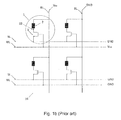
- Figs 1a and 1b illustrate an equivalent circuit of a conventional memory device formed from an array comprising a plurality of thermally assisted switching magnetic random access memory (TAS-MRAM) cells 1.
- TAS-MRAM thermally assisted switching magnetic random access memory
- Each TAS-MRAM cell 1 comprises a magnetic tunnel junction represented by the numeral 2 in Figs 1a and 1b , and a select transistor 3, electrically connected to the magnetic tunnel junction 2.
- the magnetic tunnel junction 2 can be formed of a reference layer having a fixed magnetization, a storage layer having a direction that can be switched from a first stable direction to a second stable direction upon writing of the cell, and an insulating layer between the storage layer and the sense layer.
- the magnetic tunnel junction 2 can further comprise a first antiferromagnetic layer (not shown) pinning the magnetization of the reference layer and providing the fixed magnetization of the reference layer and a second antiferromagnetic layer (also not shown) pinning the storage layer when the magnetic tunnel junction 2 is at a temperature that is below a critical temperature of the second antiferromagnetic layer.
- the array comprises a plurality of bit lines BL and a word lines WL, each bit line BL and each word line WL addressing a row and a column of the array, respectively. More particularly, the bit lines BL and word lines WL are electrically connected to the drain and gate of the select transistor 3, respectively. In the arrangement of Figs. 1a and 1b , the source of the select transistors 3 are grounded through a plurality of source lines SL connected to rows of TAS-MRAM cells 1 of the array.
- one of the TAS-MRAM cells 1 is selectively written by supplying a maximum voltage Vdd BL to one of the bit lines BL, and supplying a maximum voltage Vdd WL to one of the word lines WL.
- the respective values of Vdd BL and Vdd WL are determined by the specifications of the select transistor 3.
- the select transistor 3 of the selected TAS-MRAM cell 1 is in a passing mode by applying the voltage Vdd WL to its gate, via the word line WL.
- the write bias voltage Vmtj must be high enough to pass a heating current 31 through the magnetic tunnel junction 2 capable of heating the TAS-MRAM cell 1 above the critical temperature of the antiferromagnetic layer in order to free the magnetization of the storage layer.
- means of switching the magnetization of the storage layer are applied.
- Means of switching can comprise a magnetic field generated by a field current (not shown) passing through field lines (also not represented). Means of switching can also comprise passing a spin transfer torque current (not shown) through the magnetic tunnel junction 2, via the activated bit line BL, the storage layer magnetization being then switched by the so-called spin transfer torque (STT) effect.
- STT spin transfer torque
- the select transistor 3 can be set in a blocked mode by deselecting the activated word line WL or bit line BL, causing the magnetic tunnel junction 2 to cool down below the critical temperature, where the storage layer magnetization is "frozen" in the written direction.
- the select transistor 3 of the selected TAS-MRAM cell 1 (shown encircled in Fig. 1 b) is set in a passing mode by applying a voltage V DD to its gate, via the word line WL.
- a relatively low read bias voltage V R is applied to the magnetic tunnel junction 2, via the bit line BL, in order to pass a sense current 32 through the magnetic tunnel junction 2.
- the sense current 32 allows for measuring a junction resistance R of the magnetic tunnel junction 2, which value corresponds to the written direction of the reference layer magnetization relative to the magnetization of the reference layer.
- the write bias voltage V mtj is typically equal or greater than 1 V, its value being primarily limited by the breakdown voltage of the magnetic tunnel junction 2.
- the select transistor 3 When sinking the corresponding heating current 31, the select transistor 3 operates in its linear region. Since the select transistor 3 is operating below its saturation region, sinking the large heating current 31 requires the select transistor 3 to have a large size. Consequently, the size of the TAS-MRAM cell 1 becomes dominated by the size of the select transistor 3.
- the present application discloses a memory device which overcomes at least some limitations of the prior art.
- a memory device comprising a plurality of magnetoresistive random access memory (MRAM) cells arranged in rows and columns, each MRAM cell comprising a magnetic tunnel junction and a select transistor; a plurality of word lines, each word line connecting MRAM cells along a row via the gate of their select transistor; a plurality of bit lines, each bit line connecting MRAM cells along a column; and a plurality of source lines, each source line connecting MRAM cells along a row; characterized in that one end of the magnetic tunnel junction being electrically coupled to the source of the select transistor; each bit line connecting the MRAM cells via the drain of their select transistor; and each source line connecting the MRAM cells via the other end of the magnetic tunnel junction.
- MRAM magnetoresistive random access memory
- the present application also pertains to a method comprising, during a write operation, selectively writing one of the TAS-MRAM cells by applying a word write bias voltage and a source write bias voltage, respectively to the word line and source line connected to the selected TAS-MRAM cells, and grounding the bit line connected to the selected TAS-MRAM cells; and unselecting TAS-MRAM cells being in the same row as the TAS-MRAM cell being selectively written by applying via the corresponding bit line a bit bias voltage having a value corresponding substantially to the word write bias voltage, and unselecting other TAS-MRAM cells by grounding the corresponding word lines.
- the memory device disclosed herein allows for using select transistors with smaller size than the ones used in conventional memory devices, hence, decreasing the overall size of the memory device. Memory devices having high density and low power consumption can then be achieved.
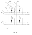
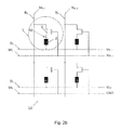
- Figs. 2a and 2b represent an equivalent circuit of a memory device 10 formed from an array comprising a plurality of thermally assisted switching magnetoresistive random access memory (TAS-MRAM) cells 1 arranged in a plurality of rows and columns, according to an embodiment.
- TAS-MRAM thermally assisted switching magnetoresistive random access memory
- FIGs 2a and 2b only four TAS-MRAM cells 1 are shown.
- Each TAS-MRAM cell 1 comprises a magnetic tunnel junction 2 and a select transistor 3 electrically coupled to the magnetic tunnel junction 2.
- the memory device 10 further comprises a plurality of bit lines BL and select lines SL, orthogonal with the bit lines BL.
- Each bit line BL connect TAS-MRAM cells 1 along a column via the source of their respective select transistor 3, and each select line SL connecting TAS-MRAM (cells 1 along a row via their respective magnetic tunnel junction 2.
- the memory device 10 further comprises a plurality of word lines WL, parallel to the select lines SL, and connecting MRAM cells 1 along a columns via the gate of their respective select transistor 3.
- the magnetic tunnel junction 2 can be formed from a reference layer having a fixed magnetization, a storage layer having a magnetization that can be switched from a first stable direction to a second stable direction, and an insulating layer between the reference and storage layers.
- the magnetic tunnel junction 2 can further comprise a first antiferromagnetic layer pinning the magnetization of the reference layer and providing its fixed magnetization, and a second antiferromagnetic layer pinning the storage layer when the magnetic tunnel junction 2 is at a temperature that is below a high threshold temperature of the second antiferromagnetic layer.
- one of the TAS-MRAM cells 1 can be selectively written by addressing the corresponding word, bit and source lines WL, BL, SL with appropriate voltage values.
- the memory cell 1 is represented where the one TAS-MRAM cell 1 being written, or selected, is shown encircled. More particularly, during a write operation a word write bias voltage V WL_w and a source write bias voltage V SL_w are applied, respectively to the word line WL and source line SL connected to the selected TAS-MRAM cell 1.
- the word write bias voltage V WL_w set the select transistor 3 of the selected TAS-MRAM cell 1 in a passing mode.
- the bit line BL connected to the selected TAS-MRAM cell 1 is grounded (GND).
- the source write bias voltage V SL_w has a value that is higher than the word write bias voltage V WL_w , such as to pass a drain current 31 through the magnetic tunnel junction 2 of the selected TAS-MRAM cell 1.
- the values of the source write bias voltage, V SL_w and the word write bias voltage V WL_w can be such that the magnitude of the drain current 31 corresponds substantially to the magnitude of the saturation drain current of the select transistor 3.
- the source write bias voltage V SL_w is higher than the transistor saturation drain voltage V Dsat by a value of V mtj_w , corresponding to the write bias junction voltage across the magnetic tunnel junction 2 when passing the drain current 31.
- V WL_w may be convenient to set the value of V WL_w to V DD and V SL_w to a value corresponding to V DD + V mtj w , as far as such voltage, value is compatible with foundry design rules for gate oxide, or specifications of the select transistor 3, in order to avoid damaging the select transistor gate oxide.
- the drain current is used as a heating current 31 for heating the magnetic tunnel junction 2 of the selected TAS-MRAM cell 1 above the high threshold temperature, in order to free the magnetization of the corresponding storage layer.
- the heating current 31 corresponds to the saturation drain current of the select transistor 3, allowing the size of the select transistor 3 required for sourcing the heating current 31 to be minimized.
- the storage layer magnetization of the heated magnetic tunnel junction 2 is switched by switching means comprising a magnetic field, generated by passing a field current (not shown) through the bit line BL addressing the selected TAS-MRAM cell 1 or through separate field lines (not shown).
- Switching means can also comprise passing a spin-polarized current (not shown) through the heated magnetic tunnel junction 2 of the selected TAS-MRAM cell 1, via the corresponding addressing bit line BL. In the latter case, the magnetization of the storage layer is switched by the so-called spin transfer torque (STT) effect.
- STT spin transfer torque
- the other TAS-MRAM cells 1 being connected to the activated source line SL, or in the same row as the selected TAS-MRAM cell 1 (the TAS-MRAM cell 1 at the right of the selected one in Fig. 2a ), are unselected (or not being written) by applying, via the corresponding bit line BL., a bit bias voltage V BL _ w having a value corresponding substantially to the word write bias voltage V WL_w , such that the difference between the values of V BL_w and V WL_w is null, or at least; low enough to cut off any significant leakage current of the corresponding select transistors 3.
- the other TAS-MRAM cells 1 on the other rows can be undetected by grounding (GND) the word lines WL addressing them, setting the select transistor 3 in a blocked mode.
- the corresponding source lines SL are set to a bias voltage of V DD or is floating (float).
- bit lines BL addressing the unselected TAS-MRAM cells 1 being set at the bit bias voltage V BL_w are reverse body biased (backbiased) with the high (source-substrate) source write bias voltage V SL_w. Consequently, very low sub-threshold leakage of the corresponding select transistors 3 due to body effect can be achieved.
- This allows using high-power, low threshold voltage (low VT) transistors as select transistor 3.
- the low VT transistors have a saturation current that is typically 20% higher than the one of conventional transistors, and are optimized for high currents. Consequently, the size of the select transistor 3 can be reduced, hence reducing the size of the memory device 10.
- the smaller select transistor size also allows for minimizing variations in the select transistor current due to smaller parasitic currents than the ones occurring in larger memory arrays.
- one of the TAS-MRAM cells 1 can be selectively read by addressing the gate of its select transistor 3 with a word read bias voltage V WL_r via the corresponding word line WL, setting the transistor 3 in a passing mode.
- a bit read bias voltage V BL_r and a source read bias voltage V SL_r are applied respectively to the bit line BL and source line SL addressing the selected TA5-MRAM cell 1.
- the word read bias voltage V WL_r is higher than the source read bias voltage V SL_r , such as to generate a sense voltage V sense and pass a sense current 32 through the magnetic tunnel junction 2 of the selected MRAM cell 1.
- the bit read bias voltage V BL_r then has a value corresponding to the source read bias voltage V SL_r minus the sense voltage V sense minus the voltage drop V Drop of the select transistor 3.
- V Drop corresponds to the V DS drop across the transistor.
- the sense current 32 flowing through the magnetic tunnel junction 2, via the bit line BL can then be sensed to determine the junction resistance R of the magnetic tunnel junction 2, using a conventional current sensing technique.
- the value of the determined junction resistance R corresponds to the written direction of the storage layer magnetization relative to the magnetization of the reference layer.
- the junction resistance R can be determined using a voltage sensing technique.
- the select transistor 3 be operated in its linear region where the small-signal resistance of the TAS-MRAM cell 1 is low enough to allow sensing of the magnetoresistance change in the magnetic tunnel junction 2 in series with the select transistor 3. This can be achieved by applying to the gate of the select transistor 3 of the selected TAS-MRAM cell 1 the word read bias voltage V WL_r having a value as high as is practical for the circuit design. However, the word read bias voltage V WL_r must not be so high to damage the gate oxide of the select transistor 3, and/or impair the long-term reliability of the TAS-MRAM cell 1.
- the word read bias voltage V WL_r can have a value of V DD +, Where V DD + corresponds to V DD + ⁇ V, ⁇ V being an extra voltage generating the sense voltage V sense such that the sense current 32 is large enough for sensing.
- the sense voltage V sense has a value of about 300 mV, yielding a high magnetoresistance and avoiding significant heating of the magnetic tunnel junction 2.
- the other TAS-MRAM cells 1 being connected to the activated source line SL, or in the same row as the selected TAS-MRAM cell 1 (the TAS-MRAM cell 1 at the right of the selected one in Fig. 2b ), are unselected (or not being read) by applying, via the corresponding bit lines BL, a bit bias voltage V BL_r having a value corresponding to the word read bias voltage V WL_r (such that the difference between the values of V BL_r and V WL_r is null).
- the other TAS-MRAM cells 1 on the other rows can be unselected by grounding (GND) the word lines WL addressing them, setting the select transistor 3 in a blocked mode.
- the corresponding source lines SL are set to a bias voltage of V DD or is floating (float).
- the bit write bias voltage V BL_w applied to the selected bit line BL and the bit read bias voltage V BL , applied to the deselected bit line BL during the write and read operations, respectively, can have the same value.
- the source write bias voltage V SL_w and the source read bias voltage V SL_r will in turn bias the selected source line SL through the magnetic tunnel junctions 2 of the unselected TAS-MRAM cells 1 connected to the same selected source line SL.
- Table 1 summarizes the different values of the bit, source and word bias voyages applied to the bit, word and source lines BL, WL, SL during the write and read operations for the selected and unselected lines, respectively.
- the memory device arrangement according to the embodiments can be used for any type of MRAM cells where maximizing the current density is desirable, such as STT, etc., and in not limited to TAS-MRAM cells.
Landscapes
- Engineering & Computer Science (AREA)
- Computer Hardware Design (AREA)
- Mram Or Spin Memory Techniques (AREA)
- Hall/Mr Elements (AREA)
Abstract
Description
- The present disclosure generally relates to a memory device comprising a plurality of selectable magnetoresistive random access memory (MRAM) cells. More particularly, the present disclosure concerns an arrangement of the memory device in order to minimize the size of the MRAM cells and decrease power consumption of the memory device.
-
Figs 1a and1b illustrate an equivalent circuit of a conventional memory device formed from an array comprising a plurality of thermally assisted switching magnetic random access memory (TAS-MRAM)cells 1. Four such TAS-MRAM cells 1 are represented infigures 1a and1b . - Each TAS-
MRAM cell 1 comprises a magnetic tunnel junction represented by thenumeral 2 inFigs 1a and 1b , and aselect transistor 3, electrically connected to themagnetic tunnel junction 2. Although not represented in thefigures 1a and1b , themagnetic tunnel junction 2 can be formed of a reference layer having a fixed magnetization, a storage layer having a direction that can be switched from a first stable direction to a second stable direction upon writing of the cell, and an insulating layer between the storage layer and the sense layer. Themagnetic tunnel junction 2 can further comprise a first antiferromagnetic layer (not shown) pinning the magnetization of the reference layer and providing the fixed magnetization of the reference layer and a second antiferromagnetic layer (also not shown) pinning the storage layer when themagnetic tunnel junction 2 is at a temperature that is below a critical temperature of the second antiferromagnetic layer. - The array comprises a plurality of bit lines BL and a word lines WL, each bit line BL and each word line WL addressing a row and a column of the array, respectively. More particularly, the bit lines BL and word lines WL are electrically connected to the drain and gate of the
select transistor 3, respectively. In the arrangement ofFigs. 1a and1b , the source of theselect transistors 3 are grounded through a plurality of source lines SL connected to rows of TAS-MRAM cells 1 of the array. - During a write operation (
Fig. 1a ) one of the TAS-MRAM cells 1 is selectively written by supplying a maximum voltage VddBL to one of the bit lines BL, and supplying a maximum voltage VddWL to one of the word lines WL. The selected TAS-MRAM cell 1, lying at the intersection of the activated bit line BL and word line WL, is shown encircled inFig. 1a . The respective values of VddBL and VddWL are determined by the specifications of theselect transistor 3. - More particularly, during the write operation, the
select transistor 3 of the selected TAS-MRAM cell 1 is in a passing mode by applying the voltage VddWL to its gate, via the word line WL. The voltage VddBL applied on the bit line BL results in a voltage of VDS = Vdd - Vmtj at the drain of theselect transistor 3, where Vmtj is the write bias voltage across themagnetic tunnel junction 2. The write bias voltage Vmtj must be high enough to pass aheating current 31 through themagnetic tunnel junction 2 capable of heating the TAS-MRAM cell 1 above the critical temperature of the antiferromagnetic layer in order to free the magnetization of the storage layer. During heating of the TAS-MRAM cell 1, means of switching the magnetization of the storage layer are applied. - Means of switching can comprise a magnetic field generated by a field current (not shown) passing through field lines (also not represented). Means of switching can also comprise passing a spin transfer torque current (not shown) through the
magnetic tunnel junction 2, via the activated bit line BL, the storage layer magnetization being then switched by the so-called spin transfer torque (STT) effect. - After the storage layer magnetization has been switched, the
select transistor 3 can be set in a blocked mode by deselecting the activated word line WL or bit line BL, causing themagnetic tunnel junction 2 to cool down below the critical temperature, where the storage layer magnetization is "frozen" in the written direction. - During a read operation represented in
Fig. 1b , theselect transistor 3 of the selected TAS-MRAM cell 1 (shown encircled inFig. 1 b) is set in a passing mode by applying a voltage VDD to its gate, via the word line WL. A relatively low read bias voltage VR, of about 300mV, is applied to themagnetic tunnel junction 2, via the bit line BL, in order to pass asense current 32 through themagnetic tunnel junction 2. Thesense current 32 allows for measuring a junction resistance R of themagnetic tunnel junction 2, which value corresponds to the written direction of the reference layer magnetization relative to the magnetization of the reference layer. - During the write operation, the write bias voltage Vmtj is typically equal or greater than 1 V, its value being primarily limited by the breakdown voltage of the
magnetic tunnel junction 2. When sinking thecorresponding heating current 31, theselect transistor 3 operates in its linear region. Since theselect transistor 3 is operating below its saturation region, sinking thelarge heating current 31 requires theselect transistor 3 to have a large size. Consequently, the size of the TAS-MRAM cell 1 becomes dominated by the size of theselect transistor 3. - The present application discloses a memory device which overcomes at least some limitations of the prior art.
- According to the embodiments, a memory device comprising a plurality of magnetoresistive random access memory (MRAM) cells arranged in rows and columns, each MRAM cell comprising a magnetic tunnel junction and a select transistor; a plurality of word lines, each word line connecting MRAM cells along a row via the gate of their select transistor; a plurality of bit lines, each bit line connecting MRAM cells along a column; and a plurality of source lines, each source line connecting MRAM cells along a row; characterized in that one end of the magnetic tunnel junction being electrically coupled to the source of the select transistor; each bit line connecting the MRAM cells via the drain of their select transistor; and each source line connecting the MRAM cells via the other end of the magnetic tunnel junction.
- The present application also pertains to a method comprising, during a write operation, selectively writing one of the TAS-MRAM cells by applying a word write bias voltage and a source write bias voltage, respectively to the word line and source line connected to the selected TAS-MRAM cells, and grounding the bit line connected to the selected TAS-MRAM cells; and unselecting TAS-MRAM cells being in the same row as the TAS-MRAM cell being selectively written by applying via the corresponding bit line a bit bias voltage having a value corresponding substantially to the word write bias voltage, and unselecting other TAS-MRAM cells by grounding the corresponding word lines.
- The memory device disclosed herein allows for using select transistors with smaller size than the ones used in conventional memory devices, hence, decreasing the overall size of the memory device. Memory devices having high density and low power consumption can then be achieved.
- The disclosure will be better understood with the aid of the description of an embodiment given by way of example and illustrated by the figures, in which:
-
Fig. 1a illustrates an equivalent circuit of a conventional memory device during a write operation; -
Fig. 1b illustrates an equivalent circuit of a conventional memory device during a read operation; -
Fig. 2a represents an equivalent circuit of a memory device during a write operation according to an embodiment; and -
Fig. 2b represents an equivalent circuit of a memory device during a read operation according to an embodiment. -
Figs. 2a and2b represent an equivalent circuit of amemory device 10 formed from an array comprising a plurality of thermally assisted switching magnetoresistive random access memory (TAS-MRAM)cells 1 arranged in a plurality of rows and columns, according to an embodiment. InFigs 2a and2b , only four TAS-MRAM cells 1 are shown. Each TAS-MRAM cell 1 comprises amagnetic tunnel junction 2 and aselect transistor 3 electrically coupled to themagnetic tunnel junction 2. Thememory device 10 further comprises a plurality of bit lines BL and select lines SL, orthogonal with the bit lines BL. Each bit line BL connect TAS-MRAM cells 1 along a column via the source of their respectiveselect transistor 3, and each select line SL connecting TAS-MRAM (cells 1 along a row via their respectivemagnetic tunnel junction 2. In the example ofFigs. 2a and2b , thememory device 10 further comprises a plurality of word lines WL, parallel to the select lines SL, and connectingMRAM cells 1 along a columns via the gate of their respectiveselect transistor 3. - In an embodiment not represented, the
magnetic tunnel junction 2 can be formed from a reference layer having a fixed magnetization, a storage layer having a magnetization that can be switched from a first stable direction to a second stable direction, and an insulating layer between the reference and storage layers. Themagnetic tunnel junction 2 can further comprise a first antiferromagnetic layer pinning the magnetization of the reference layer and providing its fixed magnetization, and a second antiferromagnetic layer pinning the storage layer when themagnetic tunnel junction 2 is at a temperature that is below a high threshold temperature of the second antiferromagnetic layer. - During a write operation, one of the TAS-
MRAM cells 1 can be selectively written by addressing the corresponding word, bit and source lines WL, BL, SL with appropriate voltage values. InFig. 2a , thememory cell 1 is represented where the one TAS-MRAM cell 1 being written, or selected, is shown encircled. More particularly, during a write operation a word write bias voltage VWL_w and a source write bias voltage VSL_w are applied, respectively to the word line WL and source line SL connected to the selected TAS-MRAM cell 1. The word write bias voltage VWL_w set theselect transistor 3 of the selected TAS-MRAM cell 1 in a passing mode. The bit line BL connected to the selected TAS-MRAM cell 1 is grounded (GND). - In an embodiment, the source write bias voltage VSL_w has a value that is higher than the word write bias voltage VWL_w, such as to pass a drain current 31 through the
magnetic tunnel junction 2 of the selected TAS-MRAM cell 1. The values of the source write bias voltage, VSL_w and the word write bias voltage VWL_w can be such that the magnitude of the drain current 31 corresponds substantially to the magnitude of the saturation drain current of theselect transistor 3. Preferably, the source write bias voltage VSL_w is higher than the transistor saturation drain voltage VDsat by a value of Vmtj_w, corresponding to the write bias junction voltage across themagnetic tunnel junction 2 when passing the drain current 31. It may be convenient to set the value of VWL_w to VDD and VSL_w to a value corresponding to VDD + Vmtj w, as far as such voltage, value is compatible with foundry design rules for gate oxide, or specifications of theselect transistor 3, in order to avoid damaging the select transistor gate oxide. - In an embodiment, the drain current is used as a heating current 31 for heating the
magnetic tunnel junction 2 of the selected TAS-MRAM cell 1 above the high threshold temperature, in order to free the magnetization of the corresponding storage layer. In the case theselect transistor 3 is biased at its saturation voltage, the heating current 31 corresponds to the saturation drain current of theselect transistor 3, allowing the size of theselect transistor 3 required for sourcing the heating current 31 to be minimized. - During the write operation, the storage layer magnetization of the heated
magnetic tunnel junction 2 is switched by switching means comprising a magnetic field, generated by passing a field current (not shown) through the bit line BL addressing the selected TAS-MRAM cell 1 or through separate field lines (not shown). Switching means can also comprise passing a spin-polarized current (not shown) through the heatedmagnetic tunnel junction 2 of the selected TAS-MRAM cell 1, via the corresponding addressing bit line BL. In the latter case, the magnetization of the storage layer is switched by the so-called spin transfer torque (STT) effect. - In an embodiment, the other TAS-
MRAM cells 1 being connected to the activated source line SL, or in the same row as the selected TAS-MRAM cell 1 (the TAS-MRAM cell 1 at the right of the selected one inFig. 2a ), are unselected (or not being written) by applying, via the corresponding bit line BL., a bit bias voltage VBL_w having a value corresponding substantially to the word write bias voltage VWL_w, such that the difference between the values of VBL_w and VWL_w is null, or at least; low enough to cut off any significant leakage current of the correspondingselect transistors 3. - The other TAS-
MRAM cells 1 on the other rows (the two lower TAS-MRAM cells onFig. 2a ) can be undetected by grounding (GND) the word lines WL addressing them, setting theselect transistor 3 in a blocked mode. In the example ofFig. 2a , the corresponding source lines SL are set to a bias voltage of VDD or is floating (float). - The bit lines BL addressing the unselected TAS-
MRAM cells 1 being set at the bit bias voltage VBL_w are reverse body biased (backbiased) with the high (source-substrate) source write bias voltage VSL_w. Consequently, very low sub-threshold leakage of the correspondingselect transistors 3 due to body effect can be achieved. This allows using high-power, low threshold voltage (low VT) transistors asselect transistor 3. Moreover, the low VT transistors have a saturation current that is typically 20% higher than the one of conventional transistors, and are optimized for high currents. Consequently, the size of theselect transistor 3 can be reduced, hence reducing the size of thememory device 10. - Due to cut off in leakage current, lower power consumption can be achieved with the memory device according to the embodiments compared to the conventional memory devices. The smaller select transistor size also allows for minimizing variations in the select transistor current due to smaller parasitic currents than the ones occurring in larger memory arrays.
- During a read operation (see
Fig. 2b ), one of the TAS-MRAM cells 1 (shown encircled inFig. 2b ) can be selectively read by addressing the gate of itsselect transistor 3 with a word read bias voltage VWL_r via the corresponding word line WL, setting thetransistor 3 in a passing mode. A bit read bias voltage VBL_r and a source read bias voltage VSL_r are applied respectively to the bit line BL and source line SL addressing the selected TA5-MRAM cell 1. - In an embodiment, the word read bias voltage VWL_r is higher than the source read bias voltage VSL_r, such as to generate a sense voltage Vsense and pass a sense current 32 through the
magnetic tunnel junction 2 of the selectedMRAM cell 1. The bit read bias voltage VBL_r then has a value corresponding to the source read bias voltage VSL_r minus the sense voltage Vsense minus the voltage drop VDrop of theselect transistor 3. Here, VDrop corresponds to the VDS drop across the transistor. The sense current 32 flowing through themagnetic tunnel junction 2, via the bit line BL, can then be sensed to determine the junction resistance R of themagnetic tunnel junction 2, using a conventional current sensing technique. The value of the determined junction resistance R corresponds to the written direction of the storage layer magnetization relative to the magnetization of the reference layer. Alternatively, the junction resistance R can be determined using a voltage sensing technique. - In order to sense the selected TAS-
MRAM cell 1 in a reliable and robust manner, it is preferred that theselect transistor 3 be operated in its linear region where the small-signal resistance of the TAS-MRAM cell 1 is low enough to allow sensing of the magnetoresistance change in themagnetic tunnel junction 2 in series with theselect transistor 3. This can be achieved by applying to the gate of theselect transistor 3 of the selected TAS-MRAM cell 1 the word read bias voltage VWL_r having a value as high as is practical for the circuit design. However, the word read bias voltage VWL_r must not be so high to damage the gate oxide of theselect transistor 3, and/or impair the long-term reliability of the TAS-MRAM cell 1. For example, the word read bias voltage VWL_r can have a value of VDD+, Where VDD+ corresponds to VDD + ΔV, ΔV being an extra voltage generating the sense voltage Vsense such that the sense current 32 is large enough for sensing. - In a preferred embodiment, the sense voltage Vsense has a value of about 300 mV, yielding a high magnetoresistance and avoiding significant heating of the
magnetic tunnel junction 2. - In an embodiment, the other TAS-
MRAM cells 1 being connected to the activated source line SL, or in the same row as the selected TAS-MRAM cell 1 (the TAS-MRAM cell 1 at the right of the selected one inFig. 2b ), are unselected (or not being read) by applying, via the corresponding bit lines BL, a bit bias voltage VBL_r having a value corresponding to the word read bias voltage VWL_r (such that the difference between the values of VBL_r and VWL_r is null). - The other TAS-
MRAM cells 1 on the other rows (the two lower TAS-MRAM cells onFig. 2b ) can be unselected by grounding (GND) the word lines WL addressing them, setting theselect transistor 3 in a blocked mode. In the example ofFig. 2b , the corresponding source lines SL are set to a bias voltage of VDD or is floating (float). - For convenience and in order to minimize power consumption of the
memory device 1, the bit write bias voltage VBL_w applied to the selected bit line BL and the bit read bias voltage VBL, applied to the deselected bit line BL during the write and read operations, respectively, can have the same value. The source write bias voltage VSL_w and the source read bias voltage VSL_r will in turn bias the selected source line SL through themagnetic tunnel junctions 2 of the unselected TAS-MRAM cells 1 connected to the same selected source line SL.Table 1 Bit line BL Word line WL Source line SL selected unselected selected unselected selected unselected write GND VBL-w = VWL_w VWL-w >= VDD GND VSL-w = VDD + Vmtj w VSL-w = VDD or float read VBL_r = VSL_r - Vsense - Vdrop VBL_r = VWL r VWL-r = VDD, GND VSL r = VDD VSL-r = VDD or float - Table 1 summarizes the different values of the bit, source and word bias voyages applied to the bit, word and source lines BL, WL, SL during the write and read operations for the selected and unselected lines, respectively.
- The disclosure is susceptible to various modifications and alternative forms, and specific examples thereof have been shown by way of example in the drawings and are herein described in detail. It should be understood, however, that the disclosure is not to be limited to the particular forms or methods disclosed, but to the contrary, the disclosure is to cover all modifications, equivalents, and alternatives.
- For example, the memory device arrangement according to the embodiments can be used for any type of MRAM cells where maximizing the current density is desirable, such as STT, etc., and in not limited to TAS-MRAM cells.
-
- 1
- TAS-MRAM cell
- 10
- memory device
- 2
- magnetic tunnel junction
- 3
- select transistor
- 31
- heating current
- 32
- sense current
- BL
- bit line
- R
- junction resistance
- SL
- source line
- VBL_w
- bit bias voltage in the write operation
- VBL_r
- bit bias voltage in the read operation
- VDD
- Voltage
- VDD+
- voltage VDD + ΔV
- Vdrop
- voltage drop of the select transistor
- Vmtj_w
- write bias junction voltage across the magnetic tunnel junction
- Vsense
- sense voltage
- VSL_r
- source read bias voltage
- VSL_w
- source write bias voltage
- VWL_r
- word read bias voltage
- VWL_w
- word write bias voltage
- WL
- word line
Claims (15)
- A memory device (10) comprising:a plurality of magnetoresistive random access memory (MRAM) cells (1) arranged in rows and columns, each MRAM cell (1) comprising a magnetic tunnel junction (2) and a select transistor (3);a plurality of word lines (WL), each word line (WL) connecting MRAM cells (1) along a row via the gate of their select transistor (3);a plurality of bit lines (BL), each bit line (BL) connecting MRAM cells (1) along a column; anda plurality of source lines (SL), each source line (SL) connecting MRAM cells (1) along a row;
characterized in thatone end of the magnetic tunnel junction (2) being electrically coupled to the source of the select transistor (3);each bit line (BL) connecting the MRAM cells (1) via the drain of their select transistor (3); andeach source line (SL) connecting the MRAM cells (1) via the other end of the magnetic tunnel junction (2). - The memory device according to claim 1, wherein
the select transistor (3) is a high-power, low threshold voltage transistor. - The memory device according to the claims 1 or 2, wherein
the magnetic tunnel junction (2) of each MRAM cell (1) further comprises a reference layer having a fixed magnetization, a storage layer having a second magnetization switchable from a first stable direction to a second stable direction, and an insulating layer between the storage layer and the sense layer. - The memory device according to claim 3, wherein
the magnetic tunnel junction (2) further comprises a first antiferromagnetic layer pinning the magnetization of the reference layer and a second antiferromagnetic layer pinning the storage layer when the magnetic tunnel junction (2) is at a temperature that is below a high threshold temperature. - Method of writing and reading the memory device (10) according to any of the claims from 1 to 4, comprising,
during a write operation:selectively writing one of the TAS-MRAM cells (1) by applying a word write bias voltage (VWL_w) and a source write bias voltage (VSL_w), respectively to the word line (WL) and source line (SL) connected to the selected TAS-MRAM cells (1), and grounding the bit line (BL) connected to the selected TAS-MRAM cells (1); andunselecting TAS-MRAM cells (1) being in the same row as the TAS-MRAM cell (1) being selectively written by applying via the corresponding bit line (BL) a bit bias voltage (VBL_w) having a value corresponding substantially to the word write bias voltage (VWL_w), and unselecting other TAS-MRAM cells (1) by grounding the corresponding word lines (WL). - The method according to claims 5, wherein
the source write bias voltage (VSL_w) of the source line (SL) connected to the selected TAS-MRAM cells (1) has a value that is higher than the word write bias voltage (VWL_w) of the word line (WL) connected to the selected TAS-MRAM cells (1) such as to pass a heating current (31) through the magnetic tunnel junction (2) of the MRAM cell (1) being selectively written. - The method according to claim 6, wherein
the source write bias voltage (VSL_w) has a value corresponding to VDD plus the write bias junction voltage, (Vmtj_w) across the magnetic tunnel junction (2) when passing the heating current (31). - The method according to claim 6, wherein
the magnitude of the heating current (31) corresponds substantially to the magnitude of the saturation drain current of the select transistor (3). - The method according to any of the claims from 6 to 8,
wherein
prior unselecting TAS-MRAM cells (1), the method further comprises switching the magnetization of the storage layer. - The method according to claim 9, wherein
said switching the magnetization of the storage layer comprises a magnetic field generated by passing a field current in the bit line (BL) addressing said one of the TAS-MRAM cells (1) - The method according to claim 9, wherein
said switching the magnetization of the storage layer comprises passing a spin-polarized current through the magnetic tunnel junction (2) of said one of the TAS-MRAM cells (1), via the bit line (BL) addressing said one of the TAS-MRAM cells (1). - The method according to the claims 5 or 11, further comprising,
during a read operation:selectively reading one of the TAS-MRAM cells (1) by applying a word read bias voltage (VWL_r) via the word line (WL) to the gate of the select transistor (3) connected to the selected TAS-MRAM cells (1), and applying a bit read bias voltage (VBL_r) and a source read bias voltage (VSL_r) to the bit line (BL) and source line (SL) addressing the selected TAS-MRAM cell (1); andunselecting TAS-MRAM cells (1) being in the same row as the TAS-MRAM cell 1 being selectively read by applying, via the corresponding bit lines (BL), a bit bias voltage (VBL_r) having a value corresponding to the source read bias voltage (VSL_r), and unselecting other TAS-MRAM cells (1) by grounding the corresponding word lines (WL). - The method according to claim from 12, wherein
the word read bias voltage (VWL_r) of the word line (WL) connected to the selected TAS-MRAM cells (1) is higher than the source read bias voltage (VSL_r), such as to generate a sense voltage (Vsense) and pass a sense current (32) through the magnetic tunnel junction (2) of the selected TAS-MRAM cell (1). - The method according to claim 13, wherein
the word read bias voltage (VWL_r) is such that the select transistor (3) is operated in its linear region. - The method according to claims 13 or 14, wherein
the sense voltage (Vsense) is 300 mV.
Priority Applications (3)
| Application Number | Priority Date | Filing Date | Title |
|---|---|---|---|
| EP10290102.2A EP2363862B1 (en) | 2010-03-02 | 2010-03-02 | MRAM-based memory device with rotated gate |
| JP2011043545A JP2011181168A (en) | 2010-03-02 | 2011-03-01 | Mram-based memory device with rotation gate |
| US13/038,473 US8542525B2 (en) | 2010-03-02 | 2011-03-02 | MRAM-based memory device with rotated gate |
Applications Claiming Priority (1)
| Application Number | Priority Date | Filing Date | Title |
|---|---|---|---|
| EP10290102.2A EP2363862B1 (en) | 2010-03-02 | 2010-03-02 | MRAM-based memory device with rotated gate |
Publications (2)
| Publication Number | Publication Date |
|---|---|
| EP2363862A1 true EP2363862A1 (en) | 2011-09-07 |
| EP2363862B1 EP2363862B1 (en) | 2016-10-26 |
Family
ID=42790613
Family Applications (1)
| Application Number | Title | Priority Date | Filing Date |
|---|---|---|---|
| EP10290102.2A Active EP2363862B1 (en) | 2010-03-02 | 2010-03-02 | MRAM-based memory device with rotated gate |
Country Status (3)
| Country | Link |
|---|---|
| US (1) | US8542525B2 (en) |
| EP (1) | EP2363862B1 (en) |
| JP (1) | JP2011181168A (en) |
Cited By (1)
| Publication number | Priority date | Publication date | Assignee | Title |
|---|---|---|---|---|
| EP4210058A1 (en) * | 2022-01-11 | 2023-07-12 | Antaios | Magneto resistive memory device |
Families Citing this family (11)
| Publication number | Priority date | Publication date | Assignee | Title |
|---|---|---|---|---|
| EP2405438B1 (en) * | 2010-07-07 | 2016-04-20 | Crocus Technology S.A. | Method for writing in a MRAM-based memory device with reduced power consumption |
| US8681529B2 (en) | 2011-11-10 | 2014-03-25 | Micron Technology, Inc. | Apparatuses and operation methods associated with resistive memory cell arrays with separate select lines |
| US9047965B2 (en) * | 2011-12-20 | 2015-06-02 | Everspin Technologies, Inc. | Circuit and method for spin-torque MRAM bit line and source line voltage regulation |
| KR20130093394A (en) | 2012-02-14 | 2013-08-22 | 삼성전자주식회사 | Resistive memory device performing write operation using multi-mode switching current, memory system including the same, and method of writing data in a resistive memory device |
| JP5603895B2 (en) * | 2012-03-21 | 2014-10-08 | 株式会社東芝 | Semiconductor memory device driving method and semiconductor memory device |
| US9064590B2 (en) * | 2012-03-02 | 2015-06-23 | Kabushiki Kaisha Toshiba | Driving method of semiconductor storage device and semiconductor storage device |
| KR102124209B1 (en) | 2014-04-14 | 2020-06-18 | 삼성전자주식회사 | Semiconductor memory device |
| US9647032B2 (en) * | 2014-08-27 | 2017-05-09 | Avalanche Technology, Inc. | Spin-orbitronics device and applications thereof |
| CN110197680B (en) * | 2018-02-24 | 2021-11-23 | 上海磁宇信息科技有限公司 | MRAM memory chip adopting fully-depleted silicon-on-insulator FD-SOI field effect transistor |
| JP2021048223A (en) * | 2019-09-18 | 2021-03-25 | キオクシア株式会社 | Non-volatile storage device |
| US20220172762A1 (en) * | 2020-11-30 | 2022-06-02 | Arm Limited | Ramp Write Techniques |
Citations (2)
| Publication number | Priority date | Publication date | Assignee | Title |
|---|---|---|---|---|
| WO2005043545A1 (en) * | 2003-10-31 | 2005-05-12 | Agency For Science, Technology And Research | Nano-contacted magnetic memory device |
| US20090316476A1 (en) * | 2008-06-18 | 2009-12-24 | Crocus Technology S.A. | Shared line magnetic random access memory cells |
Family Cites Families (9)
| Publication number | Priority date | Publication date | Assignee | Title |
|---|---|---|---|---|
| JP2004158119A (en) * | 2002-11-06 | 2004-06-03 | Sharp Corp | Nonvolatile semiconductor memory device |
| JP4124635B2 (en) * | 2002-12-05 | 2008-07-23 | シャープ株式会社 | Semiconductor memory device and memory cell array erasing method |
| JP4349866B2 (en) * | 2003-09-02 | 2009-10-21 | 三洋電機株式会社 | FSK signal demodulation circuit |
| JP4192060B2 (en) * | 2003-09-12 | 2008-12-03 | シャープ株式会社 | Nonvolatile semiconductor memory device |
| JP4626253B2 (en) * | 2004-10-08 | 2011-02-02 | ソニー株式会社 | Storage device |
| JP2008198311A (en) * | 2007-02-15 | 2008-08-28 | Renesas Technology Corp | Magnetic storage integrated circuit device |
| US20090103354A1 (en) * | 2007-10-17 | 2009-04-23 | Qualcomm Incorporated | Ground Level Precharge Bit Line Scheme for Read Operation in Spin Transfer Torque Magnetoresistive Random Access Memory |
| US8144509B2 (en) * | 2008-06-27 | 2012-03-27 | Qualcomm Incorporated | Write operation for spin transfer torque magnetoresistive random access memory with reduced bit cell size |
| JP5172555B2 (en) * | 2008-09-08 | 2013-03-27 | 株式会社東芝 | Semiconductor memory device |
-
2010
- 2010-03-02 EP EP10290102.2A patent/EP2363862B1/en active Active
-
2011
- 2011-03-01 JP JP2011043545A patent/JP2011181168A/en active Pending
- 2011-03-02 US US13/038,473 patent/US8542525B2/en active Active
Patent Citations (2)
| Publication number | Priority date | Publication date | Assignee | Title |
|---|---|---|---|---|
| WO2005043545A1 (en) * | 2003-10-31 | 2005-05-12 | Agency For Science, Technology And Research | Nano-contacted magnetic memory device |
| US20090316476A1 (en) * | 2008-06-18 | 2009-12-24 | Crocus Technology S.A. | Shared line magnetic random access memory cells |
Cited By (2)
| Publication number | Priority date | Publication date | Assignee | Title |
|---|---|---|---|---|
| EP4210058A1 (en) * | 2022-01-11 | 2023-07-12 | Antaios | Magneto resistive memory device |
| WO2023135019A1 (en) * | 2022-01-11 | 2023-07-20 | Antaios | Magneto resistive memory device |
Also Published As
| Publication number | Publication date |
|---|---|
| US8542525B2 (en) | 2013-09-24 |
| EP2363862B1 (en) | 2016-10-26 |
| US20110216580A1 (en) | 2011-09-08 |
| JP2011181168A (en) | 2011-09-15 |
Similar Documents
| Publication | Publication Date | Title |
|---|---|---|
| EP2363862B1 (en) | MRAM-based memory device with rotated gate | |
| US10109334B2 (en) | Magnetic memory | |
| TWI478407B (en) | Method and system for providing spin transfer tunneling magnetic memories utilizing non-planar transistors | |
| US8441844B2 (en) | Method for writing in a MRAM-based memory device with reduced power consumption | |
| US6111783A (en) | MRAM device including write circuit for supplying word and bit line current having unequal magnitudes | |
| US7668005B2 (en) | Magnetic memory | |
| US7852662B2 (en) | Spin-torque MRAM: spin-RAM, array | |
| KR102023626B1 (en) | Memory device using spin hall effect and methods of manufacturing and operating the same | |
| US7577016B2 (en) | Twin-cell semiconductor memory devices | |
| US20050036361A1 (en) | Semiconductor memory device with magnetoresistance elements and method of writing data into the same | |
| US20180151210A1 (en) | Shared source line architectures of perpendicular hybrid spin-torque transfer (stt) and spin-orbit torque (sot) magnetic random access memory | |
| US6771535B2 (en) | Semiconductor device | |
| US6930911B2 (en) | Magnetic memory device, method for writing on the same and method for reading from the same | |
| US20100208516A1 (en) | Active strap magnetic random access memory cells | |
| KR100898040B1 (en) | Mram device including offset conductors | |
| US7577041B2 (en) | Semiconductor memory device and writing method thereof | |
| US7471549B2 (en) | Semiconductor memory device | |
| KR20040093149A (en) | Magnetic storage device using ferromagnetic tunnel junction element | |
| US20070069296A1 (en) | High-density high current device cell | |
| US8804408B2 (en) | Semiconductor storage device | |
| US6807087B2 (en) | Write current shunting compensation | |
| US20210098694A1 (en) | Sot multibit memory cell | |
| JP2007213639A (en) | Nonvolatile semiconductor memory | |
| CN111383691A (en) | MRAM memory device with writing state detection unit | |
| KR100680422B1 (en) | Magnetic random access memory |
Legal Events
| Date | Code | Title | Description |
|---|---|---|---|
| PUAI | Public reference made under article 153(3) epc to a published international application that has entered the european phase |
Free format text: ORIGINAL CODE: 0009012 |
|
| AK | Designated contracting states |
Kind code of ref document: A1 Designated state(s): AT BE BG CH CY CZ DE DK EE ES FI FR GB GR HR HU IE IS IT LI LT LU LV MC MK MT NL NO PL PT RO SE SI SK SM TR |
|
| AX | Request for extension of the european patent |
Extension state: AL BA ME RS |
|
| 17P | Request for examination filed |
Effective date: 20120216 |
|
| 17Q | First examination report despatched |
Effective date: 20140307 |
|
| GRAP | Despatch of communication of intention to grant a patent |
Free format text: ORIGINAL CODE: EPIDOSNIGR1 |
|
| INTG | Intention to grant announced |
Effective date: 20151030 |
|
| GRAS | Grant fee paid |
Free format text: ORIGINAL CODE: EPIDOSNIGR3 |
|
| GRAP | Despatch of communication of intention to grant a patent |
Free format text: ORIGINAL CODE: EPIDOSNIGR1 |
|
| INTG | Intention to grant announced |
Effective date: 20160316 |
|
| GRAP | Despatch of communication of intention to grant a patent |
Free format text: ORIGINAL CODE: EPIDOSNIGR1 |
|
| INTG | Intention to grant announced |
Effective date: 20160712 |
|
| GRAS | Grant fee paid |
Free format text: ORIGINAL CODE: EPIDOSNIGR3 |
|
| GRAA | (expected) grant |
Free format text: ORIGINAL CODE: 0009210 |
|
| AK | Designated contracting states |
Kind code of ref document: B1 Designated state(s): AT BE BG CH CY CZ DE DK EE ES FI FR GB GR HR HU IE IS IT LI LT LU LV MC MK MT NL NO PL PT RO SE SI SK SM TR |
|
| REG | Reference to a national code |
Ref country code: GB Ref legal event code: FG4D |
|
| REG | Reference to a national code |
Ref country code: CH Ref legal event code: EP |
|
| REG | Reference to a national code |
Ref country code: AT Ref legal event code: REF Ref document number: 840531 Country of ref document: AT Kind code of ref document: T Effective date: 20161115 |
|
| REG | Reference to a national code |
Ref country code: IE Ref legal event code: FG4D |
|
| REG | Reference to a national code |
Ref country code: DE Ref legal event code: R096 Ref document number: 602010037435 Country of ref document: DE |
|
| REG | Reference to a national code |
Ref country code: LT Ref legal event code: MG4D |
|
| PG25 | Lapsed in a contracting state [announced via postgrant information from national office to epo] |
Ref country code: LV Free format text: LAPSE BECAUSE OF FAILURE TO SUBMIT A TRANSLATION OF THE DESCRIPTION OR TO PAY THE FEE WITHIN THE PRESCRIBED TIME-LIMIT Effective date: 20161026 |
|
| REG | Reference to a national code |
Ref country code: NL Ref legal event code: MP Effective date: 20161026 |
|
| REG | Reference to a national code |
Ref country code: AT Ref legal event code: MK05 Ref document number: 840531 Country of ref document: AT Kind code of ref document: T Effective date: 20161026 |
|
| REG | Reference to a national code |
Ref country code: FR Ref legal event code: PLFP Year of fee payment: 8 |
|
| PG25 | Lapsed in a contracting state [announced via postgrant information from national office to epo] |
Ref country code: LT Free format text: LAPSE BECAUSE OF FAILURE TO SUBMIT A TRANSLATION OF THE DESCRIPTION OR TO PAY THE FEE WITHIN THE PRESCRIBED TIME-LIMIT Effective date: 20161026 Ref country code: SE Free format text: LAPSE BECAUSE OF FAILURE TO SUBMIT A TRANSLATION OF THE DESCRIPTION OR TO PAY THE FEE WITHIN THE PRESCRIBED TIME-LIMIT Effective date: 20161026 Ref country code: NO Free format text: LAPSE BECAUSE OF FAILURE TO SUBMIT A TRANSLATION OF THE DESCRIPTION OR TO PAY THE FEE WITHIN THE PRESCRIBED TIME-LIMIT Effective date: 20170126 Ref country code: GR Free format text: LAPSE BECAUSE OF FAILURE TO SUBMIT A TRANSLATION OF THE DESCRIPTION OR TO PAY THE FEE WITHIN THE PRESCRIBED TIME-LIMIT Effective date: 20170127 |
|
| PG25 | Lapsed in a contracting state [announced via postgrant information from national office to epo] |
Ref country code: NL Free format text: LAPSE BECAUSE OF FAILURE TO SUBMIT A TRANSLATION OF THE DESCRIPTION OR TO PAY THE FEE WITHIN THE PRESCRIBED TIME-LIMIT Effective date: 20161026 Ref country code: PL Free format text: LAPSE BECAUSE OF FAILURE TO SUBMIT A TRANSLATION OF THE DESCRIPTION OR TO PAY THE FEE WITHIN THE PRESCRIBED TIME-LIMIT Effective date: 20161026 Ref country code: BE Free format text: LAPSE BECAUSE OF FAILURE TO SUBMIT A TRANSLATION OF THE DESCRIPTION OR TO PAY THE FEE WITHIN THE PRESCRIBED TIME-LIMIT Effective date: 20161026 Ref country code: HR Free format text: LAPSE BECAUSE OF FAILURE TO SUBMIT A TRANSLATION OF THE DESCRIPTION OR TO PAY THE FEE WITHIN THE PRESCRIBED TIME-LIMIT Effective date: 20161026 Ref country code: AT Free format text: LAPSE BECAUSE OF FAILURE TO SUBMIT A TRANSLATION OF THE DESCRIPTION OR TO PAY THE FEE WITHIN THE PRESCRIBED TIME-LIMIT Effective date: 20161026 Ref country code: IS Free format text: LAPSE BECAUSE OF FAILURE TO SUBMIT A TRANSLATION OF THE DESCRIPTION OR TO PAY THE FEE WITHIN THE PRESCRIBED TIME-LIMIT Effective date: 20170226 Ref country code: ES Free format text: LAPSE BECAUSE OF FAILURE TO SUBMIT A TRANSLATION OF THE DESCRIPTION OR TO PAY THE FEE WITHIN THE PRESCRIBED TIME-LIMIT Effective date: 20161026 Ref country code: FI Free format text: LAPSE BECAUSE OF FAILURE TO SUBMIT A TRANSLATION OF THE DESCRIPTION OR TO PAY THE FEE WITHIN THE PRESCRIBED TIME-LIMIT Effective date: 20161026 Ref country code: PT Free format text: LAPSE BECAUSE OF FAILURE TO SUBMIT A TRANSLATION OF THE DESCRIPTION OR TO PAY THE FEE WITHIN THE PRESCRIBED TIME-LIMIT Effective date: 20170227 |
|
| REG | Reference to a national code |
Ref country code: DE Ref legal event code: R097 Ref document number: 602010037435 Country of ref document: DE |
|
| PG25 | Lapsed in a contracting state [announced via postgrant information from national office to epo] |
Ref country code: EE Free format text: LAPSE BECAUSE OF FAILURE TO SUBMIT A TRANSLATION OF THE DESCRIPTION OR TO PAY THE FEE WITHIN THE PRESCRIBED TIME-LIMIT Effective date: 20161026 Ref country code: DK Free format text: LAPSE BECAUSE OF FAILURE TO SUBMIT A TRANSLATION OF THE DESCRIPTION OR TO PAY THE FEE WITHIN THE PRESCRIBED TIME-LIMIT Effective date: 20161026 Ref country code: RO Free format text: LAPSE BECAUSE OF FAILURE TO SUBMIT A TRANSLATION OF THE DESCRIPTION OR TO PAY THE FEE WITHIN THE PRESCRIBED TIME-LIMIT Effective date: 20161026 Ref country code: SK Free format text: LAPSE BECAUSE OF FAILURE TO SUBMIT A TRANSLATION OF THE DESCRIPTION OR TO PAY THE FEE WITHIN THE PRESCRIBED TIME-LIMIT Effective date: 20161026 Ref country code: CZ Free format text: LAPSE BECAUSE OF FAILURE TO SUBMIT A TRANSLATION OF THE DESCRIPTION OR TO PAY THE FEE WITHIN THE PRESCRIBED TIME-LIMIT Effective date: 20161026 |
|
| PG25 | Lapsed in a contracting state [announced via postgrant information from national office to epo] |
Ref country code: IT Free format text: LAPSE BECAUSE OF FAILURE TO SUBMIT A TRANSLATION OF THE DESCRIPTION OR TO PAY THE FEE WITHIN THE PRESCRIBED TIME-LIMIT Effective date: 20161026 Ref country code: BG Free format text: LAPSE BECAUSE OF FAILURE TO SUBMIT A TRANSLATION OF THE DESCRIPTION OR TO PAY THE FEE WITHIN THE PRESCRIBED TIME-LIMIT Effective date: 20170126 Ref country code: SM Free format text: LAPSE BECAUSE OF FAILURE TO SUBMIT A TRANSLATION OF THE DESCRIPTION OR TO PAY THE FEE WITHIN THE PRESCRIBED TIME-LIMIT Effective date: 20161026 |
|
| PLBE | No opposition filed within time limit |
Free format text: ORIGINAL CODE: 0009261 |
|
| STAA | Information on the status of an ep patent application or granted ep patent |
Free format text: STATUS: NO OPPOSITION FILED WITHIN TIME LIMIT |
|
| 26N | No opposition filed |
Effective date: 20170727 |
|
| REG | Reference to a national code |
Ref country code: CH Ref legal event code: PL |
|
| PG25 | Lapsed in a contracting state [announced via postgrant information from national office to epo] |
Ref country code: SI Free format text: LAPSE BECAUSE OF FAILURE TO SUBMIT A TRANSLATION OF THE DESCRIPTION OR TO PAY THE FEE WITHIN THE PRESCRIBED TIME-LIMIT Effective date: 20161026 Ref country code: MC Free format text: LAPSE BECAUSE OF FAILURE TO SUBMIT A TRANSLATION OF THE DESCRIPTION OR TO PAY THE FEE WITHIN THE PRESCRIBED TIME-LIMIT Effective date: 20161026 |
|
| REG | Reference to a national code |
Ref country code: IE Ref legal event code: MM4A |
|
| PG25 | Lapsed in a contracting state [announced via postgrant information from national office to epo] |
Ref country code: LU Free format text: LAPSE BECAUSE OF NON-PAYMENT OF DUE FEES Effective date: 20170302 |
|
| PG25 | Lapsed in a contracting state [announced via postgrant information from national office to epo] |
Ref country code: IE Free format text: LAPSE BECAUSE OF NON-PAYMENT OF DUE FEES Effective date: 20170302 Ref country code: LI Free format text: LAPSE BECAUSE OF NON-PAYMENT OF DUE FEES Effective date: 20170331 Ref country code: CH Free format text: LAPSE BECAUSE OF NON-PAYMENT OF DUE FEES Effective date: 20170331 |
|
| REG | Reference to a national code |
Ref country code: FR Ref legal event code: PLFP Year of fee payment: 9 |
|
| PG25 | Lapsed in a contracting state [announced via postgrant information from national office to epo] |
Ref country code: MT Free format text: LAPSE BECAUSE OF NON-PAYMENT OF DUE FEES Effective date: 20170302 |
|
| PG25 | Lapsed in a contracting state [announced via postgrant information from national office to epo] |
Ref country code: HU Free format text: LAPSE BECAUSE OF FAILURE TO SUBMIT A TRANSLATION OF THE DESCRIPTION OR TO PAY THE FEE WITHIN THE PRESCRIBED TIME-LIMIT; INVALID AB INITIO Effective date: 20100302 |
|
| PG25 | Lapsed in a contracting state [announced via postgrant information from national office to epo] |
Ref country code: CY Free format text: LAPSE BECAUSE OF NON-PAYMENT OF DUE FEES Effective date: 20161026 |
|
| PG25 | Lapsed in a contracting state [announced via postgrant information from national office to epo] |
Ref country code: MK Free format text: LAPSE BECAUSE OF FAILURE TO SUBMIT A TRANSLATION OF THE DESCRIPTION OR TO PAY THE FEE WITHIN THE PRESCRIBED TIME-LIMIT Effective date: 20161026 |
|
| REG | Reference to a national code |
Ref country code: DE Ref legal event code: R082 Ref document number: 602010037435 Country of ref document: DE Representative=s name: BECK & ROESSIG EUROPEAN PATENT ATTORNEYS, DE Ref country code: DE Ref legal event code: R082 Ref document number: 602010037435 Country of ref document: DE Representative=s name: BECK & ROESSIG - EUROPEAN PATENT ATTORNEYS, DE |
|
| PG25 | Lapsed in a contracting state [announced via postgrant information from national office to epo] |
Ref country code: TR Free format text: LAPSE BECAUSE OF FAILURE TO SUBMIT A TRANSLATION OF THE DESCRIPTION OR TO PAY THE FEE WITHIN THE PRESCRIBED TIME-LIMIT Effective date: 20161026 |
|
| PGFP | Annual fee paid to national office [announced via postgrant information from national office to epo] |
Ref country code: FR Payment date: 20230322 Year of fee payment: 14 |
|
| P01 | Opt-out of the competence of the unified patent court (upc) registered |
Effective date: 20230620 |
|
| REG | Reference to a national code |
Ref country code: DE Ref legal event code: R081 Ref document number: 602010037435 Country of ref document: DE Owner name: CROCUS TECHNOLOGY SA, FR Free format text: FORMER OWNER: CROCUS TECHNOLOGY, GRENOBLE, FR Ref country code: DE Ref legal event code: R081 Ref document number: 602010037435 Country of ref document: DE Owner name: ALLEGRO MICRO SYSTEMS LLC, MANCHESTER, US Free format text: FORMER OWNER: CROCUS TECHNOLOGY, GRENOBLE, FR Ref country code: DE Ref legal event code: R081 Ref document number: 602010037435 Country of ref document: DE Owner name: ALLEGRO MICRO SYSTEMS LLC, WILMINGTON, US Free format text: FORMER OWNER: CROCUS TECHNOLOGY, GRENOBLE, FR |
|
| REG | Reference to a national code |
Ref country code: DE Ref legal event code: R081 Ref document number: 602010037435 Country of ref document: DE Owner name: ALLEGRO MICRO SYSTEMS LLC, MANCHESTER, US Free format text: FORMER OWNER: CROCUS TECHNOLOGY SA, GRENOBLE, FR Ref country code: DE Ref legal event code: R081 Ref document number: 602010037435 Country of ref document: DE Owner name: ALLEGRO MICRO SYSTEMS LLC, WILMINGTON, US Free format text: FORMER OWNER: CROCUS TECHNOLOGY SA, GRENOBLE, FR |
|
| REG | Reference to a national code |
Ref country code: DE Ref legal event code: R081 Ref document number: 602010037435 Country of ref document: DE Owner name: ALLEGRO MICRO SYSTEMS LLC, MANCHESTER, US Free format text: FORMER OWNER: ALLEGRO MICRO SYSTEMS LLC, WILMINGTON, DE, US |
|
| REG | Reference to a national code |
Ref country code: GB Ref legal event code: 732E Free format text: REGISTERED BETWEEN 20240229 AND 20240306 |
|
| PGFP | Annual fee paid to national office [announced via postgrant information from national office to epo] |
Ref country code: DE Payment date: 20240320 Year of fee payment: 15 Ref country code: GB Payment date: 20240320 Year of fee payment: 15 |