EP2363291A1 - Inkjet head and inkjet recording device - Google Patents
Inkjet head and inkjet recording device Download PDFInfo
- Publication number
- EP2363291A1 EP2363291A1 EP11155635A EP11155635A EP2363291A1 EP 2363291 A1 EP2363291 A1 EP 2363291A1 EP 11155635 A EP11155635 A EP 11155635A EP 11155635 A EP11155635 A EP 11155635A EP 2363291 A1 EP2363291 A1 EP 2363291A1
- Authority
- EP
- European Patent Office
- Prior art keywords
- plural
- partition walls
- piezoelectric element
- inkjet head
- nozzle plate
- Prior art date
- Legal status (The legal status is an assumption and is not a legal conclusion. Google has not performed a legal analysis and makes no representation as to the accuracy of the status listed.)
- Withdrawn
Links
- 238000005192 partition Methods 0.000 claims abstract description 39
- 239000000758 substrate Substances 0.000 claims abstract description 38
- 238000007789 sealing Methods 0.000 claims abstract description 27
- PXHVJJICTQNCMI-UHFFFAOYSA-N Nickel Chemical compound [Ni] PXHVJJICTQNCMI-UHFFFAOYSA-N 0.000 claims description 11
- 229910021421 monocrystalline silicon Inorganic materials 0.000 claims description 5
- 229910052759 nickel Inorganic materials 0.000 claims description 5
- 238000012423 maintenance Methods 0.000 claims description 3
- 230000007246 mechanism Effects 0.000 claims description 3
- 230000003134 recirculating effect Effects 0.000 claims description 3
- 238000000034 method Methods 0.000 description 14
- 238000004519 manufacturing process Methods 0.000 description 7
- 239000000463 material Substances 0.000 description 7
- 229910052451 lead zirconate titanate Inorganic materials 0.000 description 6
- 238000001312 dry etching Methods 0.000 description 4
- 238000007747 plating Methods 0.000 description 4
- 239000010931 gold Substances 0.000 description 3
- 239000007788 liquid Substances 0.000 description 3
- 238000005459 micromachining Methods 0.000 description 3
- 230000008569 process Effects 0.000 description 3
- 229910052581 Si3N4 Inorganic materials 0.000 description 2
- 239000000853 adhesive Substances 0.000 description 2
- 230000001070 adhesive effect Effects 0.000 description 2
- 238000010586 diagram Methods 0.000 description 2
- 239000003822 epoxy resin Substances 0.000 description 2
- PCHJSUWPFVWCPO-UHFFFAOYSA-N gold Chemical compound [Au] PCHJSUWPFVWCPO-UHFFFAOYSA-N 0.000 description 2
- 229910052737 gold Inorganic materials 0.000 description 2
- HFGPZNIAWCZYJU-UHFFFAOYSA-N lead zirconate titanate Chemical compound [O-2].[O-2].[O-2].[O-2].[O-2].[Ti+4].[Zr+4].[Pb+2] HFGPZNIAWCZYJU-UHFFFAOYSA-N 0.000 description 2
- 238000005498 polishing Methods 0.000 description 2
- 229920000647 polyepoxide Polymers 0.000 description 2
- 239000004065 semiconductor Substances 0.000 description 2
- HQVNEWCFYHHQES-UHFFFAOYSA-N silicon nitride Chemical compound N12[Si]34N5[Si]62N3[Si]51N64 HQVNEWCFYHHQES-UHFFFAOYSA-N 0.000 description 2
- 238000012546 transfer Methods 0.000 description 2
- 238000001039 wet etching Methods 0.000 description 2
- WSMQKESQZFQMFW-UHFFFAOYSA-N 5-methyl-pyrazole-3-carboxylic acid Chemical compound CC1=CC(C(O)=O)=NN1 WSMQKESQZFQMFW-UHFFFAOYSA-N 0.000 description 1
- PIGFYZPCRLYGLF-UHFFFAOYSA-N Aluminum nitride Chemical compound [Al]#N PIGFYZPCRLYGLF-UHFFFAOYSA-N 0.000 description 1
- 229910003327 LiNbO3 Inorganic materials 0.000 description 1
- RTAQQCXQSZGOHL-UHFFFAOYSA-N Titanium Chemical compound [Ti] RTAQQCXQSZGOHL-UHFFFAOYSA-N 0.000 description 1
- PNEYBMLMFCGWSK-UHFFFAOYSA-N aluminium oxide Inorganic materials [O-2].[O-2].[O-2].[Al+3].[Al+3] PNEYBMLMFCGWSK-UHFFFAOYSA-N 0.000 description 1
- 230000008901 benefit Effects 0.000 description 1
- 230000008859 change Effects 0.000 description 1
- 239000011248 coating agent Substances 0.000 description 1
- 238000000576 coating method Methods 0.000 description 1
- 238000005520 cutting process Methods 0.000 description 1
- 238000007599 discharging Methods 0.000 description 1
- 230000005684 electric field Effects 0.000 description 1
- 230000006872 improvement Effects 0.000 description 1
- 238000005304 joining Methods 0.000 description 1
- 238000010030 laminating Methods 0.000 description 1
- GQYHUHYESMUTHG-UHFFFAOYSA-N lithium niobate Chemical compound [Li+].[O-][Nb](=O)=O GQYHUHYESMUTHG-UHFFFAOYSA-N 0.000 description 1
- 238000012986 modification Methods 0.000 description 1
- 230000004048 modification Effects 0.000 description 1
- 238000000206 photolithography Methods 0.000 description 1
- 229920001721 polyimide Polymers 0.000 description 1
- 230000002265 prevention Effects 0.000 description 1
- 238000012545 processing Methods 0.000 description 1
- 230000009467 reduction Effects 0.000 description 1
- 230000002940 repellent Effects 0.000 description 1
- 239000005871 repellent Substances 0.000 description 1
- 238000006748 scratching Methods 0.000 description 1
- 230000002393 scratching effect Effects 0.000 description 1
- HBMJWWWQQXIZIP-UHFFFAOYSA-N silicon carbide Chemical compound [Si+]#[C-] HBMJWWWQQXIZIP-UHFFFAOYSA-N 0.000 description 1
- 238000004544 sputter deposition Methods 0.000 description 1
- 229910001220 stainless steel Inorganic materials 0.000 description 1
- 239000010935 stainless steel Substances 0.000 description 1
- 238000006467 substitution reaction Methods 0.000 description 1
- 238000007740 vapor deposition Methods 0.000 description 1
Images


Classifications
-
- B—PERFORMING OPERATIONS; TRANSPORTING
- B41—PRINTING; LINING MACHINES; TYPEWRITERS; STAMPS
- B41J—TYPEWRITERS; SELECTIVE PRINTING MECHANISMS, i.e. MECHANISMS PRINTING OTHERWISE THAN FROM A FORME; CORRECTION OF TYPOGRAPHICAL ERRORS
- B41J2/00—Typewriters or selective printing mechanisms characterised by the printing or marking process for which they are designed
- B41J2/005—Typewriters or selective printing mechanisms characterised by the printing or marking process for which they are designed characterised by bringing liquid or particles selectively into contact with a printing material
- B41J2/01—Ink jet
- B41J2/135—Nozzles
- B41J2/14—Structure thereof only for on-demand ink jet heads
- B41J2/14201—Structure of print heads with piezoelectric elements
- B41J2/14209—Structure of print heads with piezoelectric elements of finger type, chamber walls consisting integrally of piezoelectric material
-
- B—PERFORMING OPERATIONS; TRANSPORTING
- B41—PRINTING; LINING MACHINES; TYPEWRITERS; STAMPS
- B41J—TYPEWRITERS; SELECTIVE PRINTING MECHANISMS, i.e. MECHANISMS PRINTING OTHERWISE THAN FROM A FORME; CORRECTION OF TYPOGRAPHICAL ERRORS
- B41J2/00—Typewriters or selective printing mechanisms characterised by the printing or marking process for which they are designed
- B41J2/005—Typewriters or selective printing mechanisms characterised by the printing or marking process for which they are designed characterised by bringing liquid or particles selectively into contact with a printing material
- B41J2/01—Ink jet
- B41J2/135—Nozzles
- B41J2/16—Production of nozzles
- B41J2/1607—Production of print heads with piezoelectric elements
- B41J2/161—Production of print heads with piezoelectric elements of film type, deformed by bending and disposed on a diaphragm
-
- B—PERFORMING OPERATIONS; TRANSPORTING
- B41—PRINTING; LINING MACHINES; TYPEWRITERS; STAMPS
- B41J—TYPEWRITERS; SELECTIVE PRINTING MECHANISMS, i.e. MECHANISMS PRINTING OTHERWISE THAN FROM A FORME; CORRECTION OF TYPOGRAPHICAL ERRORS
- B41J2/00—Typewriters or selective printing mechanisms characterised by the printing or marking process for which they are designed
- B41J2/005—Typewriters or selective printing mechanisms characterised by the printing or marking process for which they are designed characterised by bringing liquid or particles selectively into contact with a printing material
- B41J2/01—Ink jet
- B41J2/135—Nozzles
- B41J2/16—Production of nozzles
- B41J2/1621—Manufacturing processes
- B41J2/1623—Manufacturing processes bonding and adhesion
-
- B—PERFORMING OPERATIONS; TRANSPORTING
- B41—PRINTING; LINING MACHINES; TYPEWRITERS; STAMPS
- B41J—TYPEWRITERS; SELECTIVE PRINTING MECHANISMS, i.e. MECHANISMS PRINTING OTHERWISE THAN FROM A FORME; CORRECTION OF TYPOGRAPHICAL ERRORS
- B41J2/00—Typewriters or selective printing mechanisms characterised by the printing or marking process for which they are designed
- B41J2/005—Typewriters or selective printing mechanisms characterised by the printing or marking process for which they are designed characterised by bringing liquid or particles selectively into contact with a printing material
- B41J2/01—Ink jet
- B41J2/135—Nozzles
- B41J2/16—Production of nozzles
- B41J2/1621—Manufacturing processes
- B41J2/1631—Manufacturing processes photolithography
-
- B—PERFORMING OPERATIONS; TRANSPORTING
- B41—PRINTING; LINING MACHINES; TYPEWRITERS; STAMPS
- B41J—TYPEWRITERS; SELECTIVE PRINTING MECHANISMS, i.e. MECHANISMS PRINTING OTHERWISE THAN FROM A FORME; CORRECTION OF TYPOGRAPHICAL ERRORS
- B41J2/00—Typewriters or selective printing mechanisms characterised by the printing or marking process for which they are designed
- B41J2/005—Typewriters or selective printing mechanisms characterised by the printing or marking process for which they are designed characterised by bringing liquid or particles selectively into contact with a printing material
- B41J2/01—Ink jet
- B41J2/135—Nozzles
- B41J2/16—Production of nozzles
- B41J2/1621—Manufacturing processes
- B41J2/1632—Manufacturing processes machining
-
- B—PERFORMING OPERATIONS; TRANSPORTING
- B41—PRINTING; LINING MACHINES; TYPEWRITERS; STAMPS
- B41J—TYPEWRITERS; SELECTIVE PRINTING MECHANISMS, i.e. MECHANISMS PRINTING OTHERWISE THAN FROM A FORME; CORRECTION OF TYPOGRAPHICAL ERRORS
- B41J2/00—Typewriters or selective printing mechanisms characterised by the printing or marking process for which they are designed
- B41J2/005—Typewriters or selective printing mechanisms characterised by the printing or marking process for which they are designed characterised by bringing liquid or particles selectively into contact with a printing material
- B41J2/01—Ink jet
- B41J2/135—Nozzles
- B41J2/14—Structure thereof only for on-demand ink jet heads
- B41J2/14201—Structure of print heads with piezoelectric elements
- B41J2/14209—Structure of print heads with piezoelectric elements of finger type, chamber walls consisting integrally of piezoelectric material
- B41J2002/14217—Multi layer finger type piezoelectric element
-
- B—PERFORMING OPERATIONS; TRANSPORTING
- B41—PRINTING; LINING MACHINES; TYPEWRITERS; STAMPS
- B41J—TYPEWRITERS; SELECTIVE PRINTING MECHANISMS, i.e. MECHANISMS PRINTING OTHERWISE THAN FROM A FORME; CORRECTION OF TYPOGRAPHICAL ERRORS
- B41J2/00—Typewriters or selective printing mechanisms characterised by the printing or marking process for which they are designed
- B41J2/005—Typewriters or selective printing mechanisms characterised by the printing or marking process for which they are designed characterised by bringing liquid or particles selectively into contact with a printing material
- B41J2/01—Ink jet
- B41J2/135—Nozzles
- B41J2/14—Structure thereof only for on-demand ink jet heads
- B41J2002/14475—Structure thereof only for on-demand ink jet heads characterised by nozzle shapes or number of orifices per chamber
-
- B—PERFORMING OPERATIONS; TRANSPORTING
- B41—PRINTING; LINING MACHINES; TYPEWRITERS; STAMPS
- B41J—TYPEWRITERS; SELECTIVE PRINTING MECHANISMS, i.e. MECHANISMS PRINTING OTHERWISE THAN FROM A FORME; CORRECTION OF TYPOGRAPHICAL ERRORS
- B41J2202/00—Embodiments of or processes related to ink-jet or thermal heads
- B41J2202/01—Embodiments of or processes related to ink-jet heads
- B41J2202/11—Embodiments of or processes related to ink-jet heads characterised by specific geometrical characteristics
-
- B—PERFORMING OPERATIONS; TRANSPORTING
- B41—PRINTING; LINING MACHINES; TYPEWRITERS; STAMPS
- B41J—TYPEWRITERS; SELECTIVE PRINTING MECHANISMS, i.e. MECHANISMS PRINTING OTHERWISE THAN FROM A FORME; CORRECTION OF TYPOGRAPHICAL ERRORS
- B41J2202/00—Embodiments of or processes related to ink-jet or thermal heads
- B41J2202/01—Embodiments of or processes related to ink-jet heads
- B41J2202/12—Embodiments of or processes related to ink-jet heads with ink circulating through the whole print head
Abstract
An inkjet head includes: plural piezoelectric element partition walls (14), a nozzle plate (16), a frame member (17), and a sealing member (27). The piezoelectric element partition walls are arrayed on a substrate (15) in a direction orthogonal to a predetermined ink ejecting direction and forms partition walls of plural pressure chambers (24). The nozzle plate is bonded to be crosslinked to top surfaces of the plural piezoelectric element partition walls and the plural nozzle holes (2) are formed in the nozzle plate. The frame member surrounds the piezoelectric element partition walls. The sealing member is bonded to a surface of the nozzle plate on a side not opposed to the piezoelectric element partition walls and bonded to a top surface of the frame member and has openings in positions corresponding to the plural nozzle holes.
Description
- This application is based upon and claims the benefit of priority from Japanese Application No.
2010-45099, filed on March 2, 2010 - Embodiments described herein relate generally to a technique for an arrangement structure of a nozzle plate in an inkjet head.
-
- (A) In the past, an inkjet head is known in which a projection section including a piezoelectric element is formed on a substrate, plural pressure chambers and plural piezoelectric actuators are formed by forming plural grooves in the projection section, a frame member is joined to a plane section on the substrate, and a nozzle plate are bonded to the upper surface of the frame member and the top upper surface of the projection section.
In the inkjet head, a space formed by the substrate, the frame member, the projection section, and the nozzle plate is used as an ink supply path or an ink discharge path. In the inkjet head, it is possible to forcibly supply ink from the ink supply path to the pressure chambers and discharge the ink, which is not ejected from nozzles, from the pressure chambers to the ink discharge path. Therefore, it is possible to forcibly cause convection of the ink in the pressure chambers irrespective of presence or absence of the ejection of the ink from the nozzles. Since the ink can be forcibly discharged even if air bubbles or foreign matters are mixed in the pressure chambers because of the forcible convection, it is possible to minimize a failure in which the ink is not ejected because of the air bubbles or the foreign matters. - (B) A configuration is also known in which a nozzle plate made of single crystal silicon is adopted. A large number of nozzle holes are formed in the nozzle plate by dry etching. Since the nozzle plate is made of the single crystal silicon, it is possible to easily apply a semiconductor micromachining technique such as the dry etching and form highly-accurate nozzle holes. Since the nozzle holes are highly accurately processed, it is possible to improve arrival position accuracy of liquid droplets discharged from the nozzle holes. Therefore, it is possible to improve printing quality. Alternatively, when an inkjet head is applied to manufacturing of an electronic device such as a flat panel display, it is possible to improve yield of a manufacturing process.
- It is assumed that the nozzle plate of (B) is applied to the inkjet head of (A). In this case, two problems explained below occur.
- A first problem is that it is difficult to inexpensively provide the inkjet head. Since the nozzle plate of (A) has a function of sealing not only the pressure chambers but also the ink supply path, the nozzle plate needs to have a large area. On the other hand, since nozzles are formed by the semiconductor micromachining technique in the nozzle plate of (B) , manufacturing cost for the nozzle plate is higher as the area of the nozzle plate is larger.
- A second problem is that the nozzle plate tends to be damaged in a bonding process for the nozzle plate. In a process for manufacturing the inkjet head of (A), first, the substrate is cut to form the projection section and, subsequently, the plural grooves are formed in the projection section to form the plural pressure chambers and the plural piezoelectric actuators. Subsequently, the frame member is bonded to the substrate and, finally, the nozzle plate is bonded to the upper surfaces of the projection section and the frame member. However, since the nozzle plate made of the single crystal silicon of (B) is an extremely fragile material, if there is a difference between height positions of the top surface of the projection section and the upper surface of the frame member, in some case, the nozzle plate cracks because of stress generated therein when the nozzle plate is bonded. It is conceivable to simultaneously polish the top surface of the projection section and the upper surface of the frame member to prevent a difference in level from occurring. However, since the large number of columnar piezoelectric actuators are formed among the pressure chambers on the top surface of the projection section, it is likely that the piezoelectric actuators are broken during the polishing. It is difficult to form the grooves in the projection section after polishing the projection section and the frame member. This is because, since the diameter of a rotary knife that can be used for the cutting is large compared with a space between the projection section and the frame member, even the frame member is processed when the projection section is grooved.
-
-
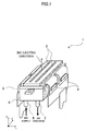
FIG. 1 is an external perspective view of an inkjet head; -
FIG. 2 is a schematic plan view of the inkjet head; -
FIG. 3 is a sectional view of the inkjet head taken along line A-A shown inFIG. 2 ; -
FIG. 4 is a sectional view of the inkjet head taken along line B-B shown inFIG. 3 ; -
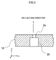
FIG. 5 is a longitudinal sectional view of a nozzle taken along a z-x plane; and -
FIG. 6 is a schematic diagram of an inkjet recording device including the inkjet head. - In general, according to one embodiment, an inkjet head includes: a substrate; plural piezoelectric element partition walls arrayed on the substrate in a direction orthogonal to a predetermined ink ejecting direction and configured to form partition walls of plural pressure chambers respectively corresponding to plural nozzle holes; a nozzle plate extending in the direction of the array of the plural piezoelectric element partition walls and bonded to be crosslinked to top surfaces of the plural piezoelectric element partition walls, the plural nozzle holes being formed in the nozzle plate; a frame member arranged on the substrate and configured to surround the piezoelectric element partition walls; and a sealing member bonded to surfaces of the nozzle plate on a side not opposed to the piezoelectric element partition walls, bonded to a top surface of the frame member, and having openings in positions corresponding to the plural nozzle holes.
- An embodiment is explained below with reference to the accompanying drawings.
-
FIG. 1 is an external perspective view of an inkjet head 1. - The inkjet head 1 includes a
head substrate 3 includingnozzles 2 from which ink is ejected,driver ICs 4 configured to generate a driving signal, and amanifold 5 including anink supply port 6 and anink discharge port 7. - The inkjet head 1 ejects ink, which is supplied from the
ink supply port 6, from thenozzles 2 according to the driving signal generated by thedriver ICs 4. The ink not ejected from thenozzles 2 of the ink flown in from theink supply port 6 is discharged from theink discharge port 7. -
FIG. 2 is a schematic plan view of the inkjet head.FIG. 3 is a sectional view of the inkjet head taken along line A-A shown inFIG. 2 .FIG. 4 is a sectional view of the inkjet head taken along line B-B shown inFIG. 3 . - The
head substrate 3 includespiezoelectric members 14, a base substrate 15 (a substrate),nozzle plates 16, aframe member 17, and asealing member 27. A space in the center surrounded by thebase substrate 15, thepiezoelectric members 14, and the sealingmember 27 forms anink supply path 18 for supplying ink topressure chambers 24. Theframe member 17 is bonded on thebase substrate 15 and surrounds thepiezoelectric members 14 and the like. - Spaces surrounded by the
base substrate 15, thepiezoelectric members 14, theframe member 17, and the sealingmember 27 formink discharge paths 19 for discharging the ink from thepressure chambers 24. - On the
base substrate 15,wiring electrodes 20 electrically connecting electrodes 21 (seeFIG. 4 ) formed on inner walls of thepressure chambers 24 and thedriver ICs 4 are formed. Further, in thebase substrate 15,ink supply holes 22 communicating with theink supply path 18 andink discharge holes 23 communicating with theink discharge paths 19 are formed. Theink supply holes 22 are hydraulically connected to theink supply port 6 by the manifold 5 (seeFIG. 1 ). Theink discharge holes 23 are hydraulically connected to theink discharge port 7 by themanifold 5. - The
base substrate 15 is desirably formed of a material having a small dielectric constant and a small difference in a coefficient of thermal expansion from that of thepiezoelectric members 14. As the material of thebase substrate 15, for example, alumina (Al2O3) , silicon nitride (Si3N4) , silicon carbide (SiC), aluminum nitride (AlN), lead zirconate titanate (PZT), or the like can be adopted. In this embodiment, as an example, PZT having a low dielectric constant is adopted. - The
piezoelectric members 14 extending in the x axis direction are joined on thebase substrate 15. Each of thepiezoelectric members 14 is formed by laminating apiezoelectric member 14a and apiezoelectric member 14b polarized in directions opposite to each other along a plate thickness direction. In thepiezoelectric member 14, plural long grooves connected from theink supply path 18 to theink discharge paths 19 are formed in parallel. Theelectrodes 21 are formed on inner surfaces of the long grooves (seeFIG. 4 ) . Spaces surrounded by the long grooves and one surfaces of thenozzle plates 16, which are provided on thepiezoelectric member 14 and cover the long grooves, are thepressure chambers 24. In this way, thenozzle plates 16 extend in the direction in which the plural piezoelectric element partition walls are arrayed (seeFIG. 2 ) and bonded to be crosslinked to the top surfaces of the plural piezoelectric element partition walls (seeFIG. 4 ) . Plural nozzle holes are formed in the nozzle plates 16 (seeFIG. 2 ) . - The
nozzle plates 16 are bonded to cover the entire region of a rectangular top surface of each of the plural piezoelectric element partition walls. In this way, thenozzle plates 16 are bonded to be closely attached to a wide range of the top surface of each of the piezoelectric element partition walls. This makes it possible to firmly bond thenozzle plates 16 to the plural piezoelectric element partition walls. - Consequently, the plural piezoelectric element partition walls including piezoelectric elements are erected on the
base substrate 15. The piezoelectric element partition walls are arrayed on thebase substrate 15 in a direction orthogonal to a predetermined ink ejecting direction. The plural piezoelectric element partition walls form partition walls of plural pressure chambers respectively corresponding to the plural nozzle holes. - In this embodiment, the plural piezoelectric element partition walls are arrayed to form parallel plural rows (two rows). The
nozzle plates 16 are arranged to be divided into two rows to correspond to the respective plural rows of the piezoelectric element partition walls. - The
electrodes 21 are connected to thedriver ICs 4 through thewiring electrodes 20. Thepiezoelectric members 14 among thepressure chambers 24 adjacent to one another are sandwiched by theelectrodes 21 provided in thepressure chambers 24 to form actuators 25 (seeFIG. 4 ). - If an electric field is applied to the
actuators 25 by the driving signal generated by thedriver ICs 4, theactuators 25 are sheared in the shape of the hiragana character "ku" to have vertexes in joining sections of thepiezoelectric member 14a and thepiezoelectric member 14b. According to the deformation of theactuators 25, the capacity of thepressure chambers 24 changes and the ink on the inside of thepressure chambers 24 is pressed. The ink pressed in thepressure chambers 24 is ejected from thenozzles 2. - Specifically, the
piezoelectric members 14 can be formed of lead zirconate titanate (PZT: Pb (Zr,Ti) O3), lithium niobate (LiNbO3) , lithium tantalate (LiTaO3) , or the like. In this embodiment, as an example, zirconate titanate (PZT) having a relatively high piezoelectric constant is adopted. - The
electrodes 21 have a two-layer structure of nickel (Ni) and gold (Au) . Theelectrodes 21 are uniformly formed in the long grooves formed in the piezoelectric members 14 (seeFIG. 4 ). As a method of forming theelectrodes 21, besides a plating method, a sputtering method, a vapor deposition method, or the like can also be adopted. Thepressure chambers 24 are formed in a shape having depth of 300 µm and width of 80 µm and arrayed in parallel at a pitch of 169 µm. -
FIG. 5 is a longitudinal sectional view of the nozzle taken along a z-x plane. In thenozzle plates 16, thenozzle 2 is formed in a position offset at every three periods from the center in a longitudinal direction of the pressure chamber 24 (the y axis direction). Thenozzle 2 has asmall hole 2a on an ink ejection side and has alarge hole 2b on thepressure chamber 24 side. The nozzle holes 2a and 2b can be formed at high accuracy by dry etching, wet etching, or the like. In this embodiment, as an example of a material of thenozzle plates 16, single crystal silicon is adopted. - As the material of the
nozzle plates 16, nickel can also be adopted. Thenozzle plates 16 can be formed by an electrocasting method. The size of thenozzle plates 16 is minimum size for covering openings of the pressure chambers 24 (e.g., width in the y axis direction is 2 mm, thickness in the z axis direction is 50 µm, and length in the x axis direction is 50 mm to 60 mm). By holding down the size of thenozzle plates 16, it is possible to increase the number of nozzle plates obtained from work performed once in a nozzle hole forming process by dry etching or wet etching. Therefore, it is possible to reduce manufacturing cost for thenozzle plates 16. - The sealing
member 27 is bonded to surfaces of thenozzle plates 16 on a side not opposed to the piezoelectric element partition walls and the top surface of theframe member 17. The sealingmember 27 seals the upper surfaces of theink supply path 18 and theink discharge paths 19. In the sealingmember 27, openings are provided in positions corresponding to the nozzles 2 (plural nozzle holes). - The sealing
member 27 is formed of a flexible material such as a polyimide film or a stainless steel plate. Therefore, even if a difference in level occurs between the surfaces of thenozzle plates 16 on the side not opposed to thepressure chambers 24 and the top surface of theframe member 17, the sealingmember 27 can be bonded. Liquid repellent coating is applied to the sealingmember 27. - A method of manufacturing the
head substrate 3 is explained below. - First, the
piezoelectric members 14 bonded in a state in which thepiezoelectric members 14 are polarized in directions opposite to each other are bonded to thebase substrate 15 in which the ink supply holes 22 and the ink discharge holes 23 are provided. Epoxy resin adhesive is used for the bonding of thepiezoelectric members 14 to thebase substrate 15. The epoxy resin adhesive is also used for bonding processing for members after the bonding of thepiezoelectric members 14. - Subsequently, the
piezoelectric members 14 and thebase substrate 15 are cut by a rotary knife having a trapezoidal section to form projections of thepiezoelectric members 14 in a trapezoidal shape on thebase substrate 15. In this embodiment, the height of thepiezoelectric members 14 in the z axis direction from the surface of thebase substrate 15 is about 500 µm. Subsequently, masks of wiring electrodes are formed on the upper surface of thebase substrate 15 by a method of photolithography. Subsequently, grooves are formed in the trapezoidal projections of thepiezoelectric members 14 by a dicer to form thepressure chambers 24 and theactuators 25. Electroless nickel plating is applied to thebase substrate 15 and thepiezoelectric members 14. - Further, electrolytic gold plating is applied on the electroless nickel plating. The
nozzle plates 16, in which a large number of thenozzles 2 are formed in advance, are bonded to the top surfaces of the projections of thepiezoelectric members 14. Theframe member 17 is bonded to the upper surface of thebase substrate 15. The sealingmember 27 is bonded to the top surface of theframe member 17 and the surfaces of thenozzle plates 16 on the side not opposed to thepressure chambers 24. - By adopting such a configuration, even if there is a difference in a height position in the z axis direction between the top surface of the
frame member 17 and the surfaces of thenozzle plates 16 on the side not opposed to thepressure chambers 24, since theflexible sealing member 27 is deformed, it is possible to facilitate work for bonding the sealingmember 27 to theframe member 17 and thenozzle plates 16. -
FIG. 6 is a schematic diagram of an inkjet recording device including the inkjet head. - As shown in the figure, in the inkjet recording device according to this embodiment, ink is supplied to the inkjet head 1 and the ink discharged from the inkjet head 1 is recirculated to the inkjet head 1 using an ink recirculating mechanism.
- Specifically, the ink recirculating mechanism includes a supply-
side ink tank 9, a discharge-side ink tank 10, a supply-sidepressure adjustment pump 11, atransfer pump 12, a discharge-sidepressure adjustment pump 13, and a tube that hydraulically connects the tanks and the pumps. - The supply-side
pressure adjustment pump 11 and the discharge-sidepressure adjustment pump 13 respectively adjust the pressure of the supply-side ink tank 9 and the pressure of the discharge-side ink tank 10. The supply-side ink tank 9 supplies the ink to theink supply port 6 of the inkjet head 1. The discharge-side ink tank 10 temporarily stores the ink discharged from theink discharge port 7 of the inkjet head 1. Thetransfer pump 12 recirculates the ink stored in the discharge-side ink tank 10 to the supply-side ink tank 9. - The inkjet recording device according to this embodiment shifts to a maintenance mode, for example, at the end of an image forming operation on a recording medium such as a sheet and executes, for example, a suction operation or a wiping operation as a part of a maintenance operation. During the wiping operation, the sealing
member 27 is wiped by a blade made of an elastic member such as rubber. - The openings formed in the sealing
member 27 are formed in a shape for not disturbing ejection of the ink from the nozzle holes 2 formed in thenozzle plates 16 and for preventing the elastic member, which is elastically deformed when the sealingmember 27 is wiped by the elastic member, from coming into contact with the surfaces of thenozzle plates 16. Consequently, in the wiping operation, the blade made of the elastic member does not come into contact with the surfaces of thenozzle plates 16. The nozzle holes on the surfaces of thenozzle plates 16 can be protected from scratching, breakage, and the like. - With the inkjet head and the inkjet recording device including the inkjet head according to this embodiment, it is possible to hold down the area of the
nozzle plates 16, in which micromachining of nozzles is necessary, to a necessary minimum area. Therefore, it is possible to minimize a failure in which the ink is not ejected because of air bubbles or foreign matters. Further, it is possible to inexpensively provide an inkjet recording device having high arriving position accuracy. - If the plural rows of the
piezoelectric members 14 are arranged as in this embodiment, thenozzle plates 16 independent from one another are separately bonded to the respective piezoelectric members formed in the plural rows. Therefore, even if relative positions of the plural rows of thepiezoelectric members 14 change because of the influence of some external force, thermal expansion, or the like, unnatural force is not applied to thenozzle plates 16. It is possible to prevent breakage of thenozzle plates 16. - Since the sealing
member 27 is made of the flexible material, even if there is a difference in a height position in the z axis direction between the top surface of theframe member 17 and the surfaces of thenozzle plates 16 on the side not opposed to the piezoelectric element partition walls, theflexible sealing member 27 is not broken. Therefore, it is possible to minimize occurrence of a failure in which the ink is not ejected because of air bubbles or foreign matters. Further, it is possible to manufacture, at high yield, an inkjet recording device having high arrival position accuracy. - As explained above in detail, with the technique described in this specification, it is possible to provide a technique for an arrangement structure of nozzle plates in an inkjet head. In particular, it is possible to provide a technique that can realize improvement of arrival position accuracy of ejected liquid droplets from nozzle holes in the inkjet head, prevention of breakage of the nozzle plates, and a reduction in cost.
- While certain embodiments have been described, these embodiments have been presented by way of example only, and are not intended to limit the scope of invention. Indeed, the novel embodiments described herein may be embodied in a variety of other forms; furthermore, various omissions, substitutions and changes in the form of the embodiments described herein may be made without departing from the spirit of the inventions. The accompanying claims and their equivalents are intended to cover such forms or modifications as would fall within the scope and spirit of the inventions.
Claims (7)
- An inkjet head comprising:a substrate;plural piezoelectric element partition walls arrayed on the substrate in a direction orthogonal to a predetermined ink ejecting direction and configured to form partition walls of plural pressure chambers respectively corresponding to plural nozzle holes;a nozzle plate extending in the direction of the array of the plural piezoelectric element partition walls and bonded to be crosslinked to top surfaces of the plural piezoelectric element partition walls, the plural nozzle holes being formed in the nozzle plate;a frame member arranged on the substrate and configured to surround the piezoelectric element partition walls; anda sealing member bonded to a surface of the nozzle plate on a side not opposed to the piezoelectric element partition walls, bonded to a top surface of the frame member, and having openings in positions corresponding to the plural nozzle holes.
- The inkjet head according to claim 1, wherein
the plural piezoelectric element partition walls are arranged to form parallel plural rows, and
the nozzle plate is arranged to be divided to correspond to the respective plural rows. - The inkjet head according to claim 1, wherein
the sealing member is wiped by an elastic member during a maintenance mode in an inkjet recording device including the inkjet head, and
the openings formed in the sealing member is formed in a shape for not disturbing discharge of ink from the nozzle holes formed in the nozzle plate and for preventing the elastic member, which is elastically deformed when the sealing member is wiped by the elastic member, from coming into contact with the nozzle plate. - The inkjet head according to claim 1, wherein the nozzle plate is bonded to cover an entire region of a top surface of each of the plural piezoelectric element partition walls.
- The inkjet head according to claim 1, wherein the sealing member is formed of a flexible member.
- The inkjet head according to claim 1, wherein the nozzle plate is formed of one of single crystal silicon and nickel.
- An inkjet recording device comprising:an inkjet head including:a substrate;plural piezoelectric element partition walls arrayed on the substrate in a direction orthogonal to a predetermined ink ejecting direction and configured to form partition walls of plural pressure chambers respectively corresponding to plural nozzle holes;a nozzle plate extending in the direction of the array of the plural piezoelectric element partition walls and bonded to be crosslinked to top surfaces of the plural piezoelectric element partition walls, the plural nozzle holes being formed in the nozzle plate;a frame member arranged on the substrate and configured to surround the piezoelectric element partition walls; anda sealing member bonded to a surface of the nozzle plate on a side not opposed to the piezoelectric element partition walls and bonded to a top surface of the frame member and having openings in positions corresponding to the plural nozzle holes; andan ink recirculating mechanism configured to supply ink to the inkjet head and recirculate the ink, which is discharged from the inkjet head, to the inkjet head.
Applications Claiming Priority (1)
| Application Number | Priority Date | Filing Date | Title |
|---|---|---|---|
| JP2010045099A JP5032613B2 (en) | 2010-03-02 | 2010-03-02 | Inkjet head, inkjet recording apparatus |
Publications (1)
| Publication Number | Publication Date |
|---|---|
| EP2363291A1 true EP2363291A1 (en) | 2011-09-07 |
Family
ID=43929222
Family Applications (1)
| Application Number | Title | Priority Date | Filing Date |
|---|---|---|---|
| EP11155635A Withdrawn EP2363291A1 (en) | 2010-03-02 | 2011-02-23 | Inkjet head and inkjet recording device |
Country Status (4)
| Country | Link |
|---|---|
| US (1) | US20110216129A1 (en) |
| EP (1) | EP2363291A1 (en) |
| JP (1) | JP5032613B2 (en) |
| CN (1) | CN102189789B (en) |
Cited By (8)
| Publication number | Priority date | Publication date | Assignee | Title |
|---|---|---|---|---|
| GB2497869A (en) * | 2011-12-21 | 2013-06-26 | Sii Printek Inc | Liquid jet head |
| GB2498094A (en) * | 2011-12-26 | 2013-07-03 | Sii Printek Inc | Liquid jet head |
| GB2536942A (en) * | 2015-04-01 | 2016-10-05 | Xaar Technology Ltd | Inkjet printhead |
| EP3508345A4 (en) * | 2016-09-05 | 2019-08-21 | Konica Minolta, Inc. | Ink jet head and ink jet recording apparatus |
| EP3670192A1 (en) * | 2018-12-21 | 2020-06-24 | Seiko Epson Corporation | Liquid ejecting head and liquid ejecting apparatus |
| EP3827991A1 (en) * | 2019-11-28 | 2021-06-02 | SII Printek Inc | Head chip, liquid jet head, and liquid jet recording device |
| EP3827993A1 (en) * | 2019-11-28 | 2021-06-02 | SII Printek Inc | Head chip, liquid jet head, and liquid jet recording device |
| EP3827992A1 (en) * | 2019-11-28 | 2021-06-02 | SII Printek Inc | Head chip, liquid jet head, and liquid jet recording device |
Families Citing this family (11)
| Publication number | Priority date | Publication date | Assignee | Title |
|---|---|---|---|---|
| JP5410486B2 (en) * | 2011-09-21 | 2014-02-05 | 富士フイルム株式会社 | Liquid discharge head, liquid discharge apparatus, and liquid discharge head abnormality detection method |
| JP5504296B2 (en) * | 2012-02-14 | 2014-05-28 | 東芝テック株式会社 | Ink jet head and method of manufacturing ink jet head |
| GB2504777A (en) * | 2012-08-10 | 2014-02-12 | Xaar Technology Ltd | Droplet ejection apparatus |
| JP2015100947A (en) * | 2013-11-22 | 2015-06-04 | 株式会社東芝 | Image formation device |
| JP6961379B2 (en) * | 2016-05-27 | 2021-11-05 | キヤノン株式会社 | Liquid discharge device |
| JP6322731B1 (en) | 2017-01-06 | 2018-05-09 | 株式会社東芝 | Inkjet recording head |
| CN107244145A (en) * | 2017-06-08 | 2017-10-13 | 翁焕榕 | Ink jet-print head and its nozzle plate, ink-jet printer |
| US20190118533A1 (en) * | 2017-10-24 | 2019-04-25 | Toshiba Tec Kabushiki Kaisha | Fluid ejection head and fluid ejection apparatus |
| CN108749329B (en) * | 2018-06-15 | 2019-07-09 | 大连瑞林数字印刷技术有限公司 | A kind of piezoelectric ink jet printing head structure for preventing ink from flowing back |
| JP7134779B2 (en) * | 2018-08-10 | 2022-09-12 | エスアイアイ・プリンテック株式会社 | LIQUID JET HEAD AND LIQUID JET RECORDING APPARATUS |
| JP7474661B2 (en) | 2020-09-02 | 2024-04-25 | エスアイアイ・プリンテック株式会社 | HEAD CHIP, LIQUID JET HEAD AND LIQUID JET RECORDING APPARATUS |
Citations (3)
| Publication number | Priority date | Publication date | Assignee | Title |
|---|---|---|---|---|
| EP0703082A2 (en) * | 1994-09-23 | 1996-03-27 | Compaq Computer Corporation | Removable orifice plate for ink jet printhead and securing apparatus |
| WO2003061975A1 (en) * | 2002-01-16 | 2003-07-31 | Xaar Technology Limited | Droplet deposition apparatus |
| JP2010045099A (en) | 2008-08-11 | 2010-02-25 | Adwelds:Kk | Display method for alignment mark image, and alignment device |
Family Cites Families (17)
| Publication number | Priority date | Publication date | Assignee | Title |
|---|---|---|---|---|
| JP3151903B2 (en) * | 1992-01-28 | 2001-04-03 | セイコーエプソン株式会社 | Ink jet recording head and recording device |
| JPH0994952A (en) * | 1995-09-28 | 1997-04-08 | Seikosha Co Ltd | Ink jet head |
| GB9710530D0 (en) * | 1997-05-23 | 1997-07-16 | Xaar Ltd | Droplet deposition apparatus and methods of manufacture thereof |
| KR100761893B1 (en) * | 1998-11-14 | 2007-09-28 | 자아 테크날러쥐 리미티드 | Droplet deposition apparatus |
| IL148024A (en) * | 1999-08-14 | 2005-07-25 | Xaar Technology Ltd | Component and method for use in a droplet deposition apparatus |
| JP2002225298A (en) * | 2001-02-01 | 2002-08-14 | Konica Corp | Ink jet recording apparatus |
| GB0121625D0 (en) * | 2001-09-07 | 2001-10-31 | Xaar Technology Ltd | Droplet deposition apparatus |
| US7537307B2 (en) * | 2005-05-30 | 2009-05-26 | Brother Kogyo Kabushiki Kaisha | Liquid-droplet jetting apparatus |
| JP2007001194A (en) * | 2005-06-24 | 2007-01-11 | Sony Corp | Head module, liquid delivering head, and liquid delivering apparatus |
| JP2007001190A (en) * | 2005-06-24 | 2007-01-11 | Sony Corp | Head module, liquid ejection head, liquid ejector and method for manufacturing head module |
| JP2007007948A (en) * | 2005-06-29 | 2007-01-18 | Sony Corp | Head module, liquid delivering head and liquid delivering apparatus |
| JP2007062367A (en) * | 2005-08-01 | 2007-03-15 | Seiko Epson Corp | Liquid jet head and liquid jet apparatus |
| JP4696993B2 (en) * | 2006-03-22 | 2011-06-08 | セイコーエプソン株式会社 | Nozzle plate, liquid jet head using the same, and method for manufacturing nozzle plate |
| GB0606685D0 (en) * | 2006-04-03 | 2006-05-10 | Xaar Technology Ltd | Droplet Deposition Apparatus |
| US8197048B2 (en) * | 2006-04-26 | 2012-06-12 | Ricoh Company, Ltd. | Image forming apparatus |
| JP4967755B2 (en) * | 2007-03-30 | 2012-07-04 | ソニー株式会社 | Head module, liquid discharge head, liquid discharge apparatus, and method of manufacturing head module |
| JP5042866B2 (en) * | 2008-01-07 | 2012-10-03 | 東芝テック株式会社 | Ink jet head, method for manufacturing ink jet head |
-
2010
- 2010-03-02 JP JP2010045099A patent/JP5032613B2/en active Active
-
2011
- 2011-02-15 CN CN201110038693XA patent/CN102189789B/en not_active Expired - Fee Related
- 2011-02-23 EP EP11155635A patent/EP2363291A1/en not_active Withdrawn
- 2011-03-01 US US13/037,552 patent/US20110216129A1/en not_active Abandoned
Patent Citations (3)
| Publication number | Priority date | Publication date | Assignee | Title |
|---|---|---|---|---|
| EP0703082A2 (en) * | 1994-09-23 | 1996-03-27 | Compaq Computer Corporation | Removable orifice plate for ink jet printhead and securing apparatus |
| WO2003061975A1 (en) * | 2002-01-16 | 2003-07-31 | Xaar Technology Limited | Droplet deposition apparatus |
| JP2010045099A (en) | 2008-08-11 | 2010-02-25 | Adwelds:Kk | Display method for alignment mark image, and alignment device |
Cited By (21)
| Publication number | Priority date | Publication date | Assignee | Title |
|---|---|---|---|---|
| US8985745B2 (en) | 2011-12-21 | 2015-03-24 | Sii Printek Inc. | Liquid jet head, liquid jet apparatus, and method of manufacturing liquid jet head |
| GB2497869A (en) * | 2011-12-21 | 2013-06-26 | Sii Printek Inc | Liquid jet head |
| GB2498094A (en) * | 2011-12-26 | 2013-07-03 | Sii Printek Inc | Liquid jet head |
| US9010907B2 (en) | 2011-12-26 | 2015-04-21 | Sii Printek Inc. | Liquid jet head, liquid jet apparatus, and method of manufacturing liquid jet head |
| GB2536942A (en) * | 2015-04-01 | 2016-10-05 | Xaar Technology Ltd | Inkjet printhead |
| WO2016156792A1 (en) * | 2015-04-01 | 2016-10-06 | Xaar Technology Limited | Inkjet printhead |
| CN107438522A (en) * | 2015-04-01 | 2017-12-05 | 萨尔技术有限公司 | Ink jet-print head |
| GB2536942B (en) * | 2015-04-01 | 2018-01-10 | Xaar Technology Ltd | Inkjet printhead |
| US10532572B2 (en) | 2015-04-01 | 2020-01-14 | Xaar Technology Limited | Inkjet printhead with staggered fluidic ports |
| US10836164B2 (en) | 2016-09-05 | 2020-11-17 | Konica Minolta, Inc. | Ink jet head and ink jet recording apparatus |
| EP3508345A4 (en) * | 2016-09-05 | 2019-08-21 | Konica Minolta, Inc. | Ink jet head and ink jet recording apparatus |
| EP3670192A1 (en) * | 2018-12-21 | 2020-06-24 | Seiko Epson Corporation | Liquid ejecting head and liquid ejecting apparatus |
| CN111347788A (en) * | 2018-12-21 | 2020-06-30 | 精工爱普生株式会社 | Liquid ejecting head and liquid ejecting apparatus |
| US10906306B2 (en) | 2018-12-21 | 2021-02-02 | Seiko Epson Corporation | Liquid ejecting head and liquid ejecting apparatus |
| US11559989B2 (en) | 2018-12-21 | 2023-01-24 | Seiko Epson Corporation | Liquid ejecting head and liquid ejecting apparatus |
| EP3827991A1 (en) * | 2019-11-28 | 2021-06-02 | SII Printek Inc | Head chip, liquid jet head, and liquid jet recording device |
| EP3827993A1 (en) * | 2019-11-28 | 2021-06-02 | SII Printek Inc | Head chip, liquid jet head, and liquid jet recording device |
| EP3827992A1 (en) * | 2019-11-28 | 2021-06-02 | SII Printek Inc | Head chip, liquid jet head, and liquid jet recording device |
| US11225079B2 (en) | 2019-11-28 | 2022-01-18 | Sii Printek Inc. | Head chip, liquid jet head, and liquid jet recording device |
| US11254132B2 (en) | 2019-11-28 | 2022-02-22 | Sii Printek Inc. | Head chip, liquid jet head, and liquid jet recording device |
| US11491787B2 (en) | 2019-11-28 | 2022-11-08 | Sii Printek Inc. | Head chip, liquid jet head, and liquid jet recording device |
Also Published As
| Publication number | Publication date |
|---|---|
| JP2011178055A (en) | 2011-09-15 |
| CN102189789A (en) | 2011-09-21 |
| JP5032613B2 (en) | 2012-09-26 |
| US20110216129A1 (en) | 2011-09-08 |
| CN102189789B (en) | 2013-12-18 |
Similar Documents
| Publication | Publication Date | Title |
|---|---|---|
| EP2363291A1 (en) | Inkjet head and inkjet recording device | |
| EP2540503B1 (en) | Liquid jet head, liquid jet apparatus, and method of manufacturing liquid jet head | |
| US7578576B2 (en) | Method of manufacturing alignment jig and liquid-jet head unit | |
| US20070263041A1 (en) | Liquid-jet head and liquid-jet apparatus | |
| US10029460B2 (en) | Inkjet head and inkjet apparatus having the same | |
| JP2017177676A (en) | Liquid discharge device | |
| JP5502020B2 (en) | Ink jet head and method of manufacturing ink jet head | |
| JP4928534B2 (en) | Inkjet head | |
| JP2007168185A (en) | Inkjet head | |
| JP4508595B2 (en) | Liquid ejecting head, manufacturing method thereof, and liquid ejecting apparatus | |
| EP3725530B1 (en) | Liquid ejecting head and liquid ejecting apparatus | |
| JP5958002B2 (en) | Droplet discharge head | |
| JP2014024275A (en) | Liquid discharge head, and image forming apparatus | |
| US20240051295A1 (en) | Liquid ejection head and printing apparatus | |
| JP7193334B2 (en) | HEAD CHIP, LIQUID JET HEAD, LIQUID JET RECORDING APPARATUS, AND HEAD CHIP MANUFACTURING METHOD | |
| EP3069880A2 (en) | Electronic device, and method for manufacturing electronic device | |
| EP4324653A1 (en) | Liquid ejecting head and liquid ejecting apparatus | |
| CN111347782B (en) | Liquid ejecting head and liquid ejecting apparatus | |
| US8152281B2 (en) | Liquid ejecting head and liquid ejecting apparatus | |
| JP2022152144A (en) | Liquid jet head and liquid jet device | |
| JP2010274526A (en) | Head and device for ejecting liquid | |
| JP5485208B2 (en) | Inkjet head | |
| US20160082727A1 (en) | Liquid ejecting head and liquid ejecting apparatus | |
| JP2003205612A (en) | Ink-jet head | |
| JP2018046173A (en) | Substrate bonding method, manufacturing method for mems device, and manufacturing method for liquid injection head |
Legal Events
| Date | Code | Title | Description |
|---|---|---|---|
| PUAI | Public reference made under article 153(3) epc to a published international application that has entered the european phase |
Free format text: ORIGINAL CODE: 0009012 |
|
| 17P | Request for examination filed |
Effective date: 20110223 |
|
| AK | Designated contracting states |
Kind code of ref document: A1 Designated state(s): AL AT BE BG CH CY CZ DE DK EE ES FI FR GB GR HR HU IE IS IT LI LT LU LV MC MK MT NL NO PL PT RO RS SE SI SK SM TR |
|
| AX | Request for extension of the european patent |
Extension state: BA ME |
|
| STAA | Information on the status of an ep patent application or granted ep patent |
Free format text: STATUS: THE APPLICATION HAS BEEN WITHDRAWN |
|
| 18W | Application withdrawn |
Effective date: 20131015 |