EP2359357B1 - Digital-drive electroluminescent display with aging compensation - Google Patents
Digital-drive electroluminescent display with aging compensation Download PDFInfo
- Publication number
- EP2359357B1 EP2359357B1 EP09801841.9A EP09801841A EP2359357B1 EP 2359357 B1 EP2359357 B1 EP 2359357B1 EP 09801841 A EP09801841 A EP 09801841A EP 2359357 B1 EP2359357 B1 EP 2359357B1
- Authority
- EP
- European Patent Office
- Prior art keywords
- voltage
- emitter
- transistor
- current
- electrode
- Prior art date
- Legal status (The legal status is an assumption and is not a legal conclusion. Google has not performed a legal analysis and makes no representation as to the accuracy of the status listed.)
- Active
Links
- 230000032683 aging Effects 0.000 title claims description 48
- 238000000034 method Methods 0.000 claims description 57
- 238000005259 measurement Methods 0.000 claims description 52
- 238000012360 testing method Methods 0.000 claims description 29
- 230000008859 change Effects 0.000 description 13
- 230000000694 effects Effects 0.000 description 13
- 238000010586 diagram Methods 0.000 description 10
- 230000008569 process Effects 0.000 description 10
- 230000008901 benefit Effects 0.000 description 9
- 235000019557 luminance Nutrition 0.000 description 9
- 229910021417 amorphous silicon Inorganic materials 0.000 description 7
- 239000011159 matrix material Substances 0.000 description 7
- 239000003990 capacitor Substances 0.000 description 5
- 238000012937 correction Methods 0.000 description 4
- 230000002431 foraging effect Effects 0.000 description 4
- 238000004519 manufacturing process Methods 0.000 description 4
- 230000037230 mobility Effects 0.000 description 4
- 229910021420 polycrystalline silicon Inorganic materials 0.000 description 4
- 229920005591 polysilicon Polymers 0.000 description 4
- XLOMVQKBTHCTTD-UHFFFAOYSA-N Zinc monoxide Chemical compound [Zn]=O XLOMVQKBTHCTTD-UHFFFAOYSA-N 0.000 description 3
- 230000003679 aging effect Effects 0.000 description 3
- 230000006399 behavior Effects 0.000 description 3
- 238000012512 characterization method Methods 0.000 description 3
- 238000005516 engineering process Methods 0.000 description 3
- 230000006870 function Effects 0.000 description 3
- 239000000463 material Substances 0.000 description 3
- 238000012986 modification Methods 0.000 description 3
- 230000004048 modification Effects 0.000 description 3
- 239000000758 substrate Substances 0.000 description 3
- 230000015556 catabolic process Effects 0.000 description 2
- 238000006731 degradation reaction Methods 0.000 description 2
- 230000006866 deterioration Effects 0.000 description 2
- 230000001747 exhibiting effect Effects 0.000 description 2
- 239000011368 organic material Substances 0.000 description 2
- 239000010409 thin film Substances 0.000 description 2
- 230000003213 activating effect Effects 0.000 description 1
- 238000013459 approach Methods 0.000 description 1
- 238000003491 array Methods 0.000 description 1
- 238000004364 calculation method Methods 0.000 description 1
- 239000003086 colorant Substances 0.000 description 1
- 238000010276 construction Methods 0.000 description 1
- 230000001419 dependent effect Effects 0.000 description 1
- 230000006872 improvement Effects 0.000 description 1
- 238000012886 linear function Methods 0.000 description 1
- 238000013507 mapping Methods 0.000 description 1
- 238000012545 processing Methods 0.000 description 1
- 239000002096 quantum dot Substances 0.000 description 1
- 230000000630 rising effect Effects 0.000 description 1
- 150000003384 small molecules Chemical class 0.000 description 1
- 230000002277 temperature effect Effects 0.000 description 1
- 230000009466 transformation Effects 0.000 description 1
- 238000000844 transformation Methods 0.000 description 1
- 239000011787 zinc oxide Substances 0.000 description 1
Images


Classifications
-
- G—PHYSICS
- G09—EDUCATION; CRYPTOGRAPHY; DISPLAY; ADVERTISING; SEALS
- G09G—ARRANGEMENTS OR CIRCUITS FOR CONTROL OF INDICATING DEVICES USING STATIC MEANS TO PRESENT VARIABLE INFORMATION
- G09G3/00—Control arrangements or circuits, of interest only in connection with visual indicators other than cathode-ray tubes
- G09G3/20—Control arrangements or circuits, of interest only in connection with visual indicators other than cathode-ray tubes for presentation of an assembly of a number of characters, e.g. a page, by composing the assembly by combination of individual elements arranged in a matrix no fixed position being assigned to or needed to be assigned to the individual characters or partial characters
- G09G3/34—Control arrangements or circuits, of interest only in connection with visual indicators other than cathode-ray tubes for presentation of an assembly of a number of characters, e.g. a page, by composing the assembly by combination of individual elements arranged in a matrix no fixed position being assigned to or needed to be assigned to the individual characters or partial characters by control of light from an independent source
-
- G—PHYSICS
- G09—EDUCATION; CRYPTOGRAPHY; DISPLAY; ADVERTISING; SEALS
- G09G—ARRANGEMENTS OR CIRCUITS FOR CONTROL OF INDICATING DEVICES USING STATIC MEANS TO PRESENT VARIABLE INFORMATION
- G09G3/00—Control arrangements or circuits, of interest only in connection with visual indicators other than cathode-ray tubes
- G09G3/20—Control arrangements or circuits, of interest only in connection with visual indicators other than cathode-ray tubes for presentation of an assembly of a number of characters, e.g. a page, by composing the assembly by combination of individual elements arranged in a matrix no fixed position being assigned to or needed to be assigned to the individual characters or partial characters
- G09G3/22—Control arrangements or circuits, of interest only in connection with visual indicators other than cathode-ray tubes for presentation of an assembly of a number of characters, e.g. a page, by composing the assembly by combination of individual elements arranged in a matrix no fixed position being assigned to or needed to be assigned to the individual characters or partial characters using controlled light sources
- G09G3/30—Control arrangements or circuits, of interest only in connection with visual indicators other than cathode-ray tubes for presentation of an assembly of a number of characters, e.g. a page, by composing the assembly by combination of individual elements arranged in a matrix no fixed position being assigned to or needed to be assigned to the individual characters or partial characters using controlled light sources using electroluminescent panels
- G09G3/32—Control arrangements or circuits, of interest only in connection with visual indicators other than cathode-ray tubes for presentation of an assembly of a number of characters, e.g. a page, by composing the assembly by combination of individual elements arranged in a matrix no fixed position being assigned to or needed to be assigned to the individual characters or partial characters using controlled light sources using electroluminescent panels semiconductive, e.g. using light-emitting diodes [LED]
- G09G3/3208—Control arrangements or circuits, of interest only in connection with visual indicators other than cathode-ray tubes for presentation of an assembly of a number of characters, e.g. a page, by composing the assembly by combination of individual elements arranged in a matrix no fixed position being assigned to or needed to be assigned to the individual characters or partial characters using controlled light sources using electroluminescent panels semiconductive, e.g. using light-emitting diodes [LED] organic, e.g. using organic light-emitting diodes [OLED]
- G09G3/3225—Control arrangements or circuits, of interest only in connection with visual indicators other than cathode-ray tubes for presentation of an assembly of a number of characters, e.g. a page, by composing the assembly by combination of individual elements arranged in a matrix no fixed position being assigned to or needed to be assigned to the individual characters or partial characters using controlled light sources using electroluminescent panels semiconductive, e.g. using light-emitting diodes [LED] organic, e.g. using organic light-emitting diodes [OLED] using an active matrix
- G09G3/3233—Control arrangements or circuits, of interest only in connection with visual indicators other than cathode-ray tubes for presentation of an assembly of a number of characters, e.g. a page, by composing the assembly by combination of individual elements arranged in a matrix no fixed position being assigned to or needed to be assigned to the individual characters or partial characters using controlled light sources using electroluminescent panels semiconductive, e.g. using light-emitting diodes [LED] organic, e.g. using organic light-emitting diodes [OLED] using an active matrix with pixel circuitry controlling the current through the light-emitting element
-
- G—PHYSICS
- G09—EDUCATION; CRYPTOGRAPHY; DISPLAY; ADVERTISING; SEALS
- G09G—ARRANGEMENTS OR CIRCUITS FOR CONTROL OF INDICATING DEVICES USING STATIC MEANS TO PRESENT VARIABLE INFORMATION
- G09G3/00—Control arrangements or circuits, of interest only in connection with visual indicators other than cathode-ray tubes
- G09G3/20—Control arrangements or circuits, of interest only in connection with visual indicators other than cathode-ray tubes for presentation of an assembly of a number of characters, e.g. a page, by composing the assembly by combination of individual elements arranged in a matrix no fixed position being assigned to or needed to be assigned to the individual characters or partial characters
- G09G3/22—Control arrangements or circuits, of interest only in connection with visual indicators other than cathode-ray tubes for presentation of an assembly of a number of characters, e.g. a page, by composing the assembly by combination of individual elements arranged in a matrix no fixed position being assigned to or needed to be assigned to the individual characters or partial characters using controlled light sources
- G09G3/30—Control arrangements or circuits, of interest only in connection with visual indicators other than cathode-ray tubes for presentation of an assembly of a number of characters, e.g. a page, by composing the assembly by combination of individual elements arranged in a matrix no fixed position being assigned to or needed to be assigned to the individual characters or partial characters using controlled light sources using electroluminescent panels
- G09G3/32—Control arrangements or circuits, of interest only in connection with visual indicators other than cathode-ray tubes for presentation of an assembly of a number of characters, e.g. a page, by composing the assembly by combination of individual elements arranged in a matrix no fixed position being assigned to or needed to be assigned to the individual characters or partial characters using controlled light sources using electroluminescent panels semiconductive, e.g. using light-emitting diodes [LED]
-
- G—PHYSICS
- G09—EDUCATION; CRYPTOGRAPHY; DISPLAY; ADVERTISING; SEALS
- G09G—ARRANGEMENTS OR CIRCUITS FOR CONTROL OF INDICATING DEVICES USING STATIC MEANS TO PRESENT VARIABLE INFORMATION
- G09G2300/00—Aspects of the constitution of display devices
- G09G2300/08—Active matrix structure, i.e. with use of active elements, inclusive of non-linear two terminal elements, in the pixels together with light emitting or modulating elements
- G09G2300/0809—Several active elements per pixel in active matrix panels
- G09G2300/0819—Several active elements per pixel in active matrix panels used for counteracting undesired variations, e.g. feedback or autozeroing
-
- G—PHYSICS
- G09—EDUCATION; CRYPTOGRAPHY; DISPLAY; ADVERTISING; SEALS
- G09G—ARRANGEMENTS OR CIRCUITS FOR CONTROL OF INDICATING DEVICES USING STATIC MEANS TO PRESENT VARIABLE INFORMATION
- G09G2320/00—Control of display operating conditions
- G09G2320/02—Improving the quality of display appearance
- G09G2320/029—Improving the quality of display appearance by monitoring one or more pixels in the display panel, e.g. by monitoring a fixed reference pixel
- G09G2320/0295—Improving the quality of display appearance by monitoring one or more pixels in the display panel, e.g. by monitoring a fixed reference pixel by monitoring each display pixel
-
- G—PHYSICS
- G09—EDUCATION; CRYPTOGRAPHY; DISPLAY; ADVERTISING; SEALS
- G09G—ARRANGEMENTS OR CIRCUITS FOR CONTROL OF INDICATING DEVICES USING STATIC MEANS TO PRESENT VARIABLE INFORMATION
- G09G2320/00—Control of display operating conditions
- G09G2320/04—Maintaining the quality of display appearance
- G09G2320/041—Temperature compensation
-
- G—PHYSICS
- G09—EDUCATION; CRYPTOGRAPHY; DISPLAY; ADVERTISING; SEALS
- G09G—ARRANGEMENTS OR CIRCUITS FOR CONTROL OF INDICATING DEVICES USING STATIC MEANS TO PRESENT VARIABLE INFORMATION
- G09G2320/00—Control of display operating conditions
- G09G2320/04—Maintaining the quality of display appearance
- G09G2320/043—Preventing or counteracting the effects of ageing
- G09G2320/045—Compensation of drifts in the characteristics of light emitting or modulating elements
-
- G—PHYSICS
- G09—EDUCATION; CRYPTOGRAPHY; DISPLAY; ADVERTISING; SEALS
- G09G—ARRANGEMENTS OR CIRCUITS FOR CONTROL OF INDICATING DEVICES USING STATIC MEANS TO PRESENT VARIABLE INFORMATION
- G09G3/00—Control arrangements or circuits, of interest only in connection with visual indicators other than cathode-ray tubes
- G09G3/20—Control arrangements or circuits, of interest only in connection with visual indicators other than cathode-ray tubes for presentation of an assembly of a number of characters, e.g. a page, by composing the assembly by combination of individual elements arranged in a matrix no fixed position being assigned to or needed to be assigned to the individual characters or partial characters
- G09G3/2007—Display of intermediate tones
- G09G3/2018—Display of intermediate tones by time modulation using two or more time intervals
- G09G3/2022—Display of intermediate tones by time modulation using two or more time intervals using sub-frames
Definitions
- the present invention relates to solid-state electroluminescent flat-panel displays and more particularly to such displays having ways to compensate for aging of the electroluminescent display components.
- Electroluminescent (EL) devices have been known for some years and have been recently used in commercial display devices. Such devices employ both active-matrix and passive-matrix control schemes and can employ a plurality of subpixels.
- each subpixel includes an EL emitter and a drive transistor for driving current through the EL emitter.
- the subpixels are typically arranged in two-dimensional arrays with a row and a column address for each subpixel, and having a data value associated with the subpixel.
- Subpixels of different colors, such as red, green, blue, and white are grouped to form pixels.
- Active-matrix EL displays can be made from various emitter technologies, including coatable-inorganic light-emitting diode, quantum-dot, and organic light-emitting diode (OLED), and various backplane technologies, including amorphous silicon (a-Si), zinc oxide, and low-temperature polysilicon (LTPS).
- emitter technologies including coatable-inorganic light-emitting diode, quantum-dot, and organic light-emitting diode (OLED), and various backplane technologies, including amorphous silicon (a-Si), zinc oxide, and low-temperature polysilicon (LTPS).
- a-Si amorphous silicon
- LTPS low-temperature polysilicon
- Some transistor technologies can produce drive transistors that have varying mobilities and threshold voltages across the surface of a display ( Kuo, Yue, ed. Thin Film Transistors: Materials and Processes, vol. 2: Polycrystalline Thin Film Transistors. Boston: Kluwer Academic Publishers, 2004. pg. 410-412 ). This produces objectionable nonuniformity. These nonuniformities are present at the time the display is sold to an end user, and so are termed initial nonuniformities, or "mura.”
- FIG. 8 shows an example histogram of subpixel luminance exhibiting differences in characteristics between subpixels. All subpixels were driven at the same level, so should have had the same luminance. As FIG. 8 shows, the resulting luminances varied by 20 percent in either direction. This results in unacceptable display performance.
- a digital drive display scans the rows multiple times per frame. Each time a row is selected in a digital drive scheme, each subpixel in the row is either activated to output light at a selected level, or inactivated to emit no light. This is different from an analog drive display, in which each subpixel is caused to emit light at one of a plurality of levels corresponding to the available code values (e.g. 256).
- Kawabe in commonly-assigned U.S. Patent Application No. 2008/088561 , teaches an improvement to the above method wherein a single shift register is used to track the multiple sequences for data writing, and a series of enable control lines are used to control which of the multiple sequences is written at a given time.
- This method uses a two-transistor, one-capacitor (2T1C) subpixel circuit.
- transistor-related mura is not the only cause of nonuniformity in an EL display.
- organic light-emitting materials in the display age and become less efficient at emitting light. Aging of an OLED emitter causes a decrease in the efficiency of the emitter, the amount of light output per unit current, and an increase in the impedance of the emitter, and thus its voltage at a given current. Both effects reduce the lifetime of the display.
- the differing organic materials can age at different rates, causing differential color aging and a display whose white point varies as the display is used.
- each individual subpixel can age at a rate different from other subpixels, resulting in display nonuniformity.
- changes in the temperature of an OLED emitter can change its voltage at a given current.
- Yamashita in U.S. Patent Application Publication No. 2006/0022305 , describes a six-transistor, two-capacitor subpixel circuit driven in a scan phase, a light emission phase, and a reset phase during which the threshold voltage of the drive transistor and the turn-on voltage of the OLED are stored on capacitors connected to the data voltage terminal.
- This method does not compensate for OLED efficiency loss, and it requires a very complex subpixel having a very small aperture ratio. Such a subpixel ages more quickly and has lower manufacturing yields.
- U.S. Patent Application Publication No. 2002/0167474 by Everitt describes a pulse width modulation driver for an OLED display.
- a video display includes a voltage driver for providing a selected voltage to drive an organic light-emitting diode in a video display.
- the voltage driver can receive voltage information from a correction table that accounts for aging, column resistance, row resistance, and other diode characteristics.
- the correction tables are calculated prior to or during normal circuit operation.
- the correction scheme is based on sending a known current through the OLED diode for a duration sufficiently long to permit the transients to settle out, and then measuring the corresponding voltage with an analog-to-digital converter (A/D) residing on the column driver.
- a calibration current source and the A/D can be switched to any column through a switching matrix.
- this technique is only applicable to passive-matrix displays, not to the higher-performance active-matrix displays which are commonly employed. Further, this technique does not include any correction for changes in OLED emitters as they age, such as OLED efficiency loss.
- Arnold et al. in U.S. Patent No. 6,995,519 , teach a method of compensating for aging of an OLED device (emitter). This method relies on the drive transistor to drive current through the OLED emitter.
- drive transistors known in the art have non-idealities that are confounded with the OLED emitter aging in this method.
- Low-temperature polysilicon (LTPS) transistors can have nonuniform threshold voltages and mobilities across the surface of a display, and amorphous silicon (a-Si)transistors have a threshold voltage which changes with use.
- the method of Arnold et al. will therefore not provide complete compensation for OLED efficiency losses in circuits wherein transistors show such effects. Additionally, when methods such as reverse bias are used to mitigate a-Si transistor threshold voltage shifts, compensation of OLED efficiency loss can become unreliable without appropriate and expensive tracking and prediction of reverse bias effects.
- Naugler et al. in U.S. Patent Application Publication No. 2008/0048951 , teach measuring the current through an OLED emitter at various gate voltages of a drive transistor to locate a point on precalculated lookup tables used for compensation.
- this method requires a large number of lookup tables, consuming a significant amount of memory.
- Document EP 2 026 319 A1 discloses an organic light emitting display, which includes: a sensing unit for extracting degradation information of an organic light emitting diode included in each of the pixels, and for transferring a first digital value and a second digital value corresponding to the extracted degradation information to a data driver; the data driver for generating data signals corresponding to second data supplied from a timing controller during a normal driving period; a first analog-digital converter for converting the voltage corresponding to the first digital value to a fourth digital value, and for converting the voltage corresponding to the second digital value to a fifth digital value; and the timing controller for storing the fourth digital value and the fifth digital value, and for changing first data supplied from an exterior in accordance with the fourth digital value and the fifth digital value to generate the second data.
- Document US 2008/252 568 A1 discloses an organic light emitting display capable of displaying an image with uniform luminance regardless of deterioration of an organic light emitting diode and threshold voltage and/or mobility of a drive transistor.
- the organic light emitting display senses deterioration of the organic light emitting diode and threshold voltage and/or mobility of a drive transistor and modifies the data supplied to the pixel according to the sensed parameters.
- Document US 2008/122 759 A1 discloses a method of compensating for changes in the threshold voltage of the drive transistor of an OLED drive circuit, comprising: providing the drive transistor with a first electrode, second electrode, and gate electrode; connecting a first voltage source to the first electrode, and an OLED device to the second electrode and to a second voltage source; providing a test voltage to the gate electrode of the drive transistor and connecting to the OLED drive circuit a test circuit that includes an adjustable current mirror that causes the voltage applied to the current mirror to be at a first test level; providing a test voltage to the gate electrode of the drive transistor and connecting the test circuit to the OLED device to produce a second test level after the drive transistor and the OLED device have aged; and using the first and second test levels to calculate a change in the voltage applied to the gate electrode of the drive transistor to compensate for aging of the drive transistor.
- Document US 2005/179 628 A1 discloses a light emitting device and method for driving the device, in which the influence of fluctuations in the characteristics among transistors is removed, so as to obtain clear multi-gray scale.
- a light emitting device and a method for driving the device are also provided, in which an age-dependent change in amount of current flowing between two electrodes of a light emitting element is reduced, so as to obtain a clear multi-gray scale display.
- Document US 2006/170 623 A1 discloses techniques for emissive pixels of flat panel displays. Specifically, pixel feedback and a combination of voltage modulation and pulse width modulation are used to improve the quality and consistency of aging pixels. Based on feedback, an image frame is divided into sub-frames of various time periods. Also based on feedback, a voltage, or voltages of different voltage levels, is (are) applied to the selected sub-frames to generate an image frame of a particular gray level. The human eye integrates the effects of the voltage and pulse width modulation techniques that are applied to the various sub-frames of the image frame, over the duration of the image frame.
- EL electroluminescent
- An advantage of this invention is an electroluminescent display, such as an OLED display, that compensates for the aging of the organic materials in the display wherein circuitry or transistor aging or nonuniformities are present, without requiring extensive or complex circuitry for accumulating a continuous measurement of subpixel use or time of operation. It is a further advantage of this invention that such compensation can be performed in displays driven by pulse- width, time-modulated signals to effect desired intensity levels at each subpixel. It is a further advantage of this invention that it uses simple voltage measurement circuitry. It is a further advantage of this invention that by making all measurements of voltage, it is more sensitive to changes than methods that measure current. It is a further advantage of this invention that a single select line can be used to enable data input and data readout.
- Characteristics of an EL emitter include its efficiency, typically expressed in cd/A or as a percentage of a reference cd/A value, and its resistance, which relates to the voltage across the emitter for a given current.
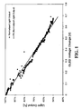
- FIG. 1 there is shown a representative relationship between efficiency and ⁇ V OLED for an OLED emitter.
- variations in the characteristics of the EL emitter e.g. efficiency, are caused by aging of the EL emitter, measured by ⁇ V OLED .
- the relationship has been experimentally determined to be approximately independent of fade current density. By measuring the luminance decrease and its relationship to ⁇ V OLED with a given current, a change in corrected signal necessary to cause an EL emitter to output a nominal luminance can be determined. This measurement can be done on a model system and thereafter stored in a lookup table or used as an algorithm.
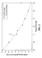
- FIG. 2 there is shown an example of the relationship between OLED emitter temperature and the OLED voltage measured at a given current density.
- variations in characteristics of the EL emitter e.g. resistance and thus voltage, are caused by variations in the temperature of the EL emitter.
- FIG. 1 and FIG. 2 show two factors known to impact the OLED voltage: aging and temperature.
- aging In order to effect an accurate compensation for the effects of aging, it is necessary to differentiate between the change in OLED voltage caused by the aging process, and that caused by changes in the temperature. Note that OLED emitter temperature is affected by ambient temperature around the display and by heat generated on the display itself.
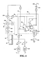
- EL display 10 includes an array of a plurality of EL subpixels 60 arranged in rows and columns.
- EL display 10 includes a plurality of row select lines 20 wherein each row of EL subpixels 60 has a row select line 20.
- EL display 10 includes a plurality of readout lines 30 wherein each column of EL subpixels 60 has a readout line 30.
- Each readout line 30 is connected to a third switch 130, which selectively connects readout line 30 to a current source 160 during the calibration process.
- connected it is meant that the elements are directly connected or connected via another component, e.g.
- each column of EL subpixels 60 also has a data line, described further below.
- the plurality of readout lines 30 is connected to one or more multiplexers 40, which permits parallel/sequential readout of signals from EL subpixels, as will become apparent.
- Multiplexer 40 can be a part of the same structure as EL display 10, or can be a separate construction that can be connected to or disconnected from EL display 10. Note that "row” and “column” do not imply any particular orientation of the display.
- Readout lines 30 are connected through third switch 130 to current source 160, as will be described below.
- the EL display 10 includes one or more temperature sensors 65 to permit measurement of the display or ambient temperature.
- the temperature sensor can be a discrete component on the driving electronics and accessed by a processing unit or integrated into a component of the driving electronics as is typical in the trade (analog-to-digital converters, microprocessors, application specific integrated circuits, etc.). Measurements of temperature can be performed and recorded during readout of signals from EL emitters in order to ascertain the impact of temperature on OLED voltage. For the description that follows, it is assumed that with this capability, we are able to then measure a signal as described, namely OLED voltage, and observe changes caused only by the aging process of the EL emitter.
- EL subpixel 60 includes an EL emitter 50, a drive transistor 70, a capacitor 75, a readout transistor 80, and a select transistor 90. Each of the transistors has a first electrode, a second electrode, and a gate electrode.
- a first voltage source 140 is selectively connected to the first electrode of drive transistor 70 by a first switch 110, which can be located on the EL display substrate or on a separate structure.
- the second electrode of drive transistor 70 is connected to EL emitter 50, and a second voltage source 150 can be selectively connected to EL emitter 50 by a second switch 120, which can also be off the EL display substrate.
- the EL emitter 50 can also be connected directly to the second voltage source 150. At least one first switch 110 and second switch 120 are provided for the EL display. Additional first and second switches can be provided if the EL display has multiple powered subgroupings of pixels.
- the drive transistor 70 can be used as the first switch 110 by operating it in reverse bias so that substantially no current flows. Methods for operating transistors in reverse bias are known in the art. In normal display mode, the first and second switches are closed, and third and fourth switches described below are open.
- the gate electrode of drive transistor 70 is connected to the second electrode of select transistor 90 to selectively provide data from data line 35 to drive transistor 70 as is well known in the art.
- the first electrode of select transistor 90 is connected to a data line 35.
- Each of the plurality of row select lines 20 is connected to the gate electrodes of the select transistors 90 in the corresponding row of EL subpixels 60.
- the gate electrode of select transistor 90 is connected to the gate electrode of readout transistor 80.
- the first electrode of readout transistor 80 is connected to the second electrode of drive transistor 70 and to EL emitter 50.
- Each of the plurality of readout lines 30 is connected to the second electrodes of the readout transistors 80 in the corresponding column of EL subpixels 60.
- Readout line 30 is connected to third switch 130.
- a respective third switch 130 (S3) is provided for each column of EL subpixels 60.
- the third switch permits current source 160 to be selectively connected to the second electrode of readout transistor 80.
- Current source 160 when connected by the third switch, provides a selected test current to EL emitter 50, causing constant current flow through the EL emitter.
- Third switch 130 and current source 160 can be provided located on or off the EL display substrate.
- the current source 160 can be used as the third switch 130 by setting it to a high-impedance (Hi-Z) mode so that substantially no current flows. Methods for setting current sources to high-impedance modes are known in the art.
- the second electrode of readout transistor 80 is also connected to a voltage measurement circuit 170, which measures voltages to provide signals representative of characteristics of EL subpixel 60.
- Voltage measurement circuit 170 includes an analog-to-digital converter 185 for converting voltage measurements into digital signals, and a processor 190. The signal from analog-to-digital converter 185 is sent to processor 190.
- Voltage measurement circuit 170 can also include a memory 195 for storing voltage measurements, and a low-pass filter 180.
- Voltage measurement circuit 170 is connected through a multiplexer output line 45 and multiplexer 40 to a plurality of readout lines 30 and readout transistors 80 for sequentially reading out the voltages from a plurality of EL subpixels 60.
- each can have its own multiplexer output line 45.
- a plurality of EL subpixels can be driven simultaneously.
- the plurality of multiplexers permits parallel reading out of the voltages from the various multiplexers 40, and each multiplexer permits sequential reading out of the readout lines 30 attached to it. This will be referred to herein as a parallel/sequential process.
- Processor 190 can also be connected to data line 35 and select line 20 by way of a control line 95 and a driver circuit 155.
- processor 190 can provide predetermined data values to data line 35, and thus to the gate electrode of drive transistor 70, during the measurement process to be described herein.
- Processor 190 can also accept display data via input signal 85 and provide compensation for changes as will be described herein, thus providing compensated data to data line 35 using driver circuit 155 during the display process.
- Driver circuit 155 is a pulse-width modulated driver circuit which can include a gate driver connected to the row select lines 20, and a source driver connected to the data lines 35, as known in the art. This permits driver circuit 155, through the source driver, to provide selected test and drive voltages through select transistor 90 to the gate electrode of drive transistor 70.
- an EL emitter 50 e.g. an OLED emitter
- its efficiency can decrease and its resistance can increase. Both of these effects can cause the amount of light emitted by an EL emitter to decrease over time. The amount of such decrease will depend upon the use of the EL emitter. Therefore, the decrease can be different for different EL emitters in a display, which effect is herein termed spatial variations in characteristics of EL emitters 50. Such spatial variations can include differences in brightness and color balance in different parts of the display, and image "burn-in" wherein an oft-displayed image (e.g. a network logo) can cause a ghost of itself to always show on the active display. It is desirable to compensate for such effects to prevent spatial variations from becoming objectionable to a viewer of the EL display.
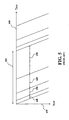
- FIG. 5 there is shown a graphical view of an embodiment of a digital drive scanning sequence according to the prior art.
- a horizontal axis 410 shows time, and a vertical axis 430 shows horizontal scanning lines.
- FIG. 5 gives an example of four-bit (sixteen code value) digital driving for ease of description.
- one cycle or frame period 420 contains a plurality of different subframes 440, 450, 460, and 470, wherein each subframe has a respective duration which is different from the duration of at least one other subframe.
- the durations are weighted so as to correspond to code values representing display element brightness. That is, the durations of N subframes within a cycle have ratios of 1 : 2 : 4 : 8 :...: 2N.
- the selected drive voltage causes the drive transistor to operate in the linear region during the on-time
- the selected black voltage causes the drive transistor to produce a current (e.g. ⁇ 10nA) which does not produce visible light from the EL emitter (e.g. ⁇ 0.1 nit emission).
- FIG. 7A and referring also to FIG. 4 , there is shown a block diagram of one embodiment of the method of the present invention.
- first switch 110, and fourth switch 131 are opened, and second switch 120 and third switch 130 are closed (Step 340).
- Select line 20 is made active for a selected row to turn on readout transistor 80 (Step 345).
- a selected test current, I testsu thus flows from current source 160 through EL emitter 50 to second voltage source 150.
- the value of current through current source 160 is selected to be less than the maximum current possible through EL emitter 50; a typical value will be in the range of 1 to 5 microamps and will be constant for all measurements during the lifetime of the EL subpixel. More than one measurement value can be used in this process, e.g. measurement can be performed at 1, 2, and 3 microamps.
- Voltage measurement circuit 170 is used to measure the voltage on readout line 30 (Step 350). This voltage is the voltage V out at the second electrode of readout transistor 80 and can be used to provide a first emitter-voltage signal V 2 that is representative of characteristics of EL emitter 50, including the resistance and efficiency of EL emitter 50.
- V 2 CV + V OLED + V read
- V out the voltage at the second electrode of readout transistor 80 (V out )
- CV is a set value and V read can be assumed to be constant as the current through the readout transistor is low and does not vary significantly over time.
- V OLED will be controlled by the value of current set by current source 160 and the current-voltage characteristics of EL emitter 50.
- V OLED can change with age-related changes in EL emitter 50.
- two separate test measurements are performed at different times.
- the first measurement is performed at a first time, e.g. when EL emitter 50 is not degraded by aging. This can be any time before EL subpixel 60 is used for display purposes.
- the value of the voltage V 2 for the first measurement is the first emitter-voltage signal (hereinafter V 2a ), and is measured and stored.
- V 2a the first emitter-voltage signal
- the measurement is repeated.
- the resulting measured V 2 is a second emitter-voltage signal (hereinafter V 2b ), and is stored.
- multiplexer 40 connected to a plurality of readout lines 30 is used to permit voltage measurement circuit 170 to sequentially measure each of a plurality of EL subpixels, e.g. every subpixel in the row (decision step 355), and provide a corresponding first and second emitter-voltage signal for each subpixel.
- Each of the plurality of EL subpixels can be driven simultaneously to advantageously reduce the time required for measurement by permitting all EL subpixels to settle simultaneously rather than sequentially. If the display is sufficiently large, it can require a plurality of multiplexers wherein the first and second emitter-voltage signals are provided in a parallel/sequential process.
- Steps 345 to 355 are repeated for each row (decision step 360).
- the EL emitter in each of the plurality of EL subpixels e.g. each EL subpixel in the row, can be provided with the selected test current simultaneously so that any settling time will have elapsed when the measurement is taken. This prevents having to wait for each subpixel to settle individually before taking a measurement.
- Changes in EL emitter 50 can cause changes to V OLED to maintain the test current I testsu . These V OLED changes will be reflected in changes to V 2 .
- the aging signal for the EL subpixel 60 can then be used to compensate for changes in characteristics of that EL subpixel.
- V OLED changes cannot be compensated with V OLED measurements alone, as V OLED changes modulate Vds of the drive transistor, affecting the whole system.
- Complete compensation can be provided by calculating a drive transistor load line, which is a Vds-Ids curve, and comparing it with an EL emitter V OLED -I OLED curve.
- FIG. 6 shows Vds on the abscissa and drain current Ids on the ordinate.
- a drive transistor load line 601 can be determined by transistor characterization and stored in a nonvolatile memory when a display is manufactured, or it can be measured for each drive transistor.
- an aged current 693 is at the intersection of an aged OLED load line 603 and drive transistor load line 601.
- One advantage of operating in the linear region is indicated by equal voltage intervals 680a and 680b.
- voltage interval 680a corresponds to current interval 681 a.
- the same voltage shift (680b) corresponds to much smaller current interval 681b. Therefore, operating in the linear region advantageously improves signal-to-noise ratio.
- Another advantage of operating in the linear region is that the behavior of the transistor can be approximated by a straight line (640) without incurring unacceptable error.
- a current sink 165 is used to measure a drive transistor load line.
- a fourth switch 131 is provided for selectively connecting the current sink 115 to the second electrode of the readout transistor.
- the current sink 165 can be used as the fourth switch 131 by setting it to a high-impedance (Hi-Z) mode so that substantially no current flows.
- a selected test voltage is provided by driver circuit 155 to the gate electrode of the drive transistor. The test voltage is preferably equal to the selected drive voltage used in normal operation of the display.
- FIG. 7B there is shown a block diagram of load line measurements according to the present invention.
- the test voltage (V data ) is provided to data line 35 (Step 310).
- the first and fourth switches are closed and the second and third switches are opened (Step 315).
- Select line 20 is made active for a selected row to provide the test voltage to the gate electrode of drive transistor 70 and to turn on readout transistor 80 (Step 320).
- a selected first current I sk,1 is provided by the current sink (Step 322) and thus flows from first voltage source 140 through the first and second electrode of drive transistor 70 and readout transistor 80 to current sink 165.
- the first current is selected to be less than the resulting current through drive transistor 70 due to the application of the test voltage; a typical value is from 1 to 5 microamps. Thus, the limiting value of current through drive transistor 70 will be controlled entirely by current sink 165, which will be the same as through drive transistor 70.
- the test voltage and first current can be selected based upon known or determined current-voltage and aging characteristics of drive transistor 70.
- Voltage measurement circuit 170 is used to measure the voltage on readout line 30, which is the voltage V out at the second electrode of readout transistor 80, providing a first transistor-voltage signal V 1T that is representative of characteristics of drive transistor 70 (Step 325). The voltage at the second electrode of readout transistor 80 (V out ) will adjust to fall on the point on the drive transistor load line corresponding to I sk,1 .
- multiplexer 40 connected to a plurality of readout lines 30 can be used to permit voltage measurement circuit 170 to sequentially read out the first signals V 1T from a plurality of EL subpixels, e.g. every subpixel in the row (decision step 330). If the display is sufficiently large, it can require a plurality of multiplexers wherein the first signal can be provided in a parallel/sequential process. If there are additional rows of subpixels to be measured (Step 335), a different row is selected by a different select line and the measurements are repeated. Multiple subpixels can be driven simultaneously with the test current, as described above in the context of EL emitter measurements.
- the drive transistor load line 601 is approximately a straight line, and so can be characterized by two points.
- the offset and slope of a linear fit 640 of the linear region of the drive transistor load line 601 are thus calculated as known in the mathematical art from the two points (V 1T , I sk,1 ) 610 and (V 2T , I sk,2 ) 611.
- First current I sk,1 is shown as 690; second current I sk,2 is shown as 691.
- the two measurements of each subpixel can be taken in either order, and the first measurement for all subpixels on all rows of the display can be taken before the second measurement of any subpixel.
- the first current can be higher or lower than the second current, so point 610 can be above point 611 instead of below it.
- EL emitter voltage can be affected by both aging effects and temperature. Measurements obtained must be adjusted for temperature variations from measurement to measurement in order to effectively compensate for both current loss and efficiency loss.
- a correlation between ambient temperature and OLED voltage can be obtained and stored as an equation or lookup table.
- FIG. 2 This relationship represents the voltage of the EL emitter over a typical operating temperature range at the current I testsu to be used for EL emitter characterization.
- the function an example of which is given by a curve fit 2, will hereinafter be denoted VbyT(T), as it provides a representative OLED voltage for each temperature T.
- the temperature in the manufacturing environment where the reference measurements are performed is likely to differ from that of the consumer environment, where subsequent measurements of the EL emitter are performed.
- T 1 the temperature of the manufacturing environment
- T 2 the temperature of the environment during measurement cycles
- first emitter-voltage signal V 2a is measured in the factory at temperature T 1
- only second emitter-voltage signal V 2b measured at temperature T 2 , is adjusted for temperature.
- FIG. 6 there is shown a graphical illustration of the effect of EL emitter aging, and in this example of OLED aging.
- An unaged OLED load line 602 shows the I-V behavior of an OLED emitter before aging.
- Aged OLED load line 603 shows the I-V behavior of the same OLED emitter after aging.
- Aged line 603 is approximately a percentage of unaged line 602.
- a point 621 indicates the OLED voltage V 2a 631, the first emitter-voltage signal, at test current 692 (I testsu ) before aging;
- a point 622 indicates an OLED voltage V 2b 632, the second emitter-voltage signal, at test current 692 after aging.
- the first emitter-voltage signal can be after aging and the second emitter-voltage signal before aging.
- Unaged OLED load line 602 can be characterized or measured for each subpixel, a group containing a plurality of subpixels, or the whole display.
- the display can be divided into multiple spatial or color (e.g. red, green, blue or white) regions, each of which can have a different unaged OLED load line curve than at least one other region.
- Unaged OLED load line(s) 602 can be stored in nonvolatile memory with the display as equation coefficient(s) or in lookup table(s).
- the drive transistor load line and thus the first and second transistor-voltage signals and the first and second currents, can therefore be used in providing the aging signal to provide complete compensation.
- the operating point of the EL subpixel after aging is point 624, the intersection of the drive transistor 601 and aged OLED 603 load lines respectively.
- the aged OLED load line 603 can be calculated according to Eq. 5. Standard mathematical techniques such as Newton's method can then be used to find the intersection of aged OLED load line 603 and drive transistor load line 601. To use Newton's method, point 621 or 622, or another point, can be used as the starting point.
- a region of the unaged OLED load line 602 close to the typical operating voltage of the system can be selected, and a linear approximation made of that region.
- the region between points 623 and 621 can be approximated with linear fit 641.
- This selection can be made at manufacturing time or while the display is operating.
- Linear fit 641 can then be multiplied by gamma to approximate the unaged OLED load line 603.
- a linear fit can be made of a region of the unaged OLED load line 603 after multiplication by gamma.
- points 622 and 625 can define a region with linear fit 642.
- the intersection point 624 between the aged OLED load line 603 and the drive transistor load line 601 can be expressed as (V ds,aged , I ds,aged ).
- the original operating point, the intersection point 621 between the unaged OLED load line 602 and the drive transistor load line 601, can be expressed as (V ds,new , I ds,new ).
- I ds,new is shown in this example as equal to test current 692 and I ds,aged is shown as current 693.
- test current I testsu 692 and I ds,new are not required to be equal.
- the present invention does require any particular value of I testsu . ⁇ V 2 , computed in Eq. 2 above, can be the aging signal for the EL subpixel and represent characteristics of the EL emitter including efficiency, as will be described below.
- the normalized current is used, as shown above in Eq. 7a, in which I norm represents the normalized current relative to its original current.
- a decrease in current can be corrected by increasing the amount of on-time for the EL emitter.
- E norm EbyV ⁇ ⁇ V 2 .
- ⁇ V 2 is as computed in Eq. 2.
- FIG. 1 shows an example of this relationship for a given OLED device.
- the relationship between current and luminance is generally linear.
- the EL emitter 50 is provided the reciprocal of the normalized efficiency in on-time. EL emitter 50 is thus activated for e.g. 1/0.77 ⁇ 1.3 times the amount of time it was before aging.
- Adjustment of the pulse-width modulated signal to obtain such increase in EL emitter 50 on-time can be performed by processor 190 using driver circuit 155.
- t E_comp represents the on-time of EL emitter 50 required to correct for the change in EL efficiency
- E norm is the efficiency of the aged EL emitter as computed in Eq. 7b
- t data is the on-time corresponding to a desired amount of light emission when the EL emitter was new.
- the two compensations are combined to produce a single selected on-time. Note that it is shown here that the light output is returned to the original value, but this is not required. For example, when temperature shifts, the entire display can be permitted to shift, assuming that temperature will affect all EL emitters equally.
- the first step in the compensation process is to drive the EL emitter in such a way that the integrated time and current are constant over time.
- Eq. 8 provides the method by which to compute the adjustment in the original amount of time the EL emitter would have been driven when it was new and flowing a full amount of current.
- t full_comp represents the amount of time required to fully compensate for the current and efficiency loss of the EL emitter
- E norm represent the normalized efficiency of the EL emitter
- t I_comp represents the on-time required to compensate for the loss in EL emitter current.
- E norm can be the aging signal for the EL subpixel, representing characteristics of the EL emitter, including the efficiency of the EL emitter.
- the aging signal for the EL emitter can include both I norm and E norm to represent the resistance and efficiency of the EL emitter.
- the aging signal can thus be 2.6, 1/2.6, or the tuples (0.5, 0.77) or (2,1.3), or some combination..
- an input signal is received (Step 375) which corresponds to the amount t data of time during a given frame which the EL emitter is to be emitting light.
- the input signal can be a digital code value, a linear intensity, an analog voltage, or other forms known in the art.
- the aging signal and the input signal can then be used to calculate a selected on-time t full_comp according to Eq. 10, above.
- the selected on-time can then be used to produce a corresponding compensated drive signal (Step 380).
- the input signal I and compensated drive signal D are four-bit code values b 3 b 2 b 1 b 0 , where each b x corresponds to the duration ratio 2 x-1 (e.g. b 3 to 8).
- the selected on-time t full_comp calculated from t data using Eq. 10 is rounded to the nearest multiple of 1/15 and multiplied by 15 to form the corresponding drive signal.
- Other transformations from on-time to drive signal known in the digital-drive art can also be employed with the present invention.
- the compensated drive signal can be computed, e.g. by processor 190, using lookup tables, piecewise linear functions, or other techniques known in the art.
- t I_comp or t E_comp can be used as the selected on-time if compensation is only desired for one effect.
- the selected drive voltage is provided (Step 385) to the gate electrode of the drive transistor for the selected on-time corresponding to compensated drive signal D .
- This selected on-time can be divided into a plurality of activated subframes, as described above. Activating the subpixel for the selected on-time compensates for variations in characteristics (e.g. voltage and efficiency) of the EL emitter according to the calculations given above.
- each subpixel When compensating an EL display having a plurality of EL subpixels, each subpixel is measured to provide a plurality of first and second emitter-voltage signals for respective subpixels, as described above.
- a respective aging signal for each subpixel is provided using the corresponding first and second emitter-voltage signals, also as described above.
- a corresponding input signal for each subpixel is received, and a corresponding compensated drive signal calculated as above using the corresponding aging signals.
- the compensated drive signal corresponding to each subpixel in the plurality of subpixels is provided to the gate electrode of that subpixel using driver circuit 155 as described above. This permits compensation for changes in characteristics of each EL emitter in the plurality of EL subpixels.
- respective first and second transistor-voltage signals for each transistor can be measured and used in producing the corresponding aging signals for each of the plurality of EL subpixels.
- the invention is employed in a display that includes Organic Light Emitting Diodes (OLEDs), which are composed of small molecule or polymeric OLEDs as disclosed in but not limited to U.S. Patent No. 4,769,292, by Tang et al. , and U.S. Patent No. 5,061,569, by VanSlyke et al . Many combinations and variations of organic light emitting materials can be used to fabricate such a display.
- OLEDs Organic Light Emitting Diodes
- the EL subpixel 60 is an OLED subpixel.
- the embodiment shown in FIG. 4 is a non-inverted, NMOS subpixel.
- the EL emitter 50 can be an OLED emitter or other emitter types known in the art.
- the drive transistor 70, and the other transistors (80, 90) can be low-temperature polysilicon (LTPS), zinc oxide (ZnO), or amorphous silicon (a-Si) transistors, or transistors of another type known in the art.
- Each transistor (70, 80, 90) can be N-channel or P-channel, and the EL emitter 50 can be connected to the drive transistor 70 in an inverted or non-inverted arrangement.
- the polarities of the first and second power supplies are reversed, and the EL emitter 50 conducts current towards the drive transistor rather than away from it.
- Current source 160 of the present invention therefore sources a negative current, that is, behaves as a current sink, to draw current through the EL emitter 50.
- current sink 165 sinks a negative current, that is, behaves as a current source, to force current through the drive transistor 70.
- the on-time of each subpixel can be continuous rather than divided into subframes, or the subframes can be in various orders. Longer subframes can be divided into multiple sub-windows, as is known in the art.
Landscapes
- Engineering & Computer Science (AREA)
- Physics & Mathematics (AREA)
- Computer Hardware Design (AREA)
- General Physics & Mathematics (AREA)
- Theoretical Computer Science (AREA)
- Control Of Indicators Other Than Cathode Ray Tubes (AREA)
- Electroluminescent Light Sources (AREA)
- Control Of El Displays (AREA)
Applications Claiming Priority (2)
| Application Number | Priority Date | Filing Date | Title |
|---|---|---|---|
| US12/337,668 US8130182B2 (en) | 2008-12-18 | 2008-12-18 | Digital-drive electroluminescent display with aging compensation |
| PCT/US2009/006594 WO2010080113A1 (en) | 2008-12-18 | 2009-12-16 | Digital-drive electroluminescent display with aging compensation |
Publications (2)
| Publication Number | Publication Date |
|---|---|
| EP2359357A1 EP2359357A1 (en) | 2011-08-24 |
| EP2359357B1 true EP2359357B1 (en) | 2015-01-21 |
Family
ID=41683267
Family Applications (1)
| Application Number | Title | Priority Date | Filing Date |
|---|---|---|---|
| EP09801841.9A Active EP2359357B1 (en) | 2008-12-18 | 2009-12-16 | Digital-drive electroluminescent display with aging compensation |
Country Status (6)
| Country | Link |
|---|---|
| US (1) | US8130182B2 (enExample) |
| EP (1) | EP2359357B1 (enExample) |
| JP (1) | JP5347033B2 (enExample) |
| KR (1) | KR101267900B1 (enExample) |
| CN (1) | CN102257554B (enExample) |
| WO (1) | WO2010080113A1 (enExample) |
Families Citing this family (39)
| Publication number | Priority date | Publication date | Assignee | Title |
|---|---|---|---|---|
| US20100277400A1 (en) * | 2009-05-01 | 2010-11-04 | Leadis Technology, Inc. | Correction of aging in amoled display |
| US10319307B2 (en) * | 2009-06-16 | 2019-06-11 | Ignis Innovation Inc. | Display system with compensation techniques and/or shared level resources |
| US10796622B2 (en) * | 2009-06-16 | 2020-10-06 | Ignis Innovation Inc. | Display system with compensation techniques and/or shared level resources |
| US8339386B2 (en) * | 2009-09-29 | 2012-12-25 | Global Oled Technology Llc | Electroluminescent device aging compensation with reference subpixels |
| US8212581B2 (en) * | 2009-09-30 | 2012-07-03 | Global Oled Technology Llc | Defective emitter detection for electroluminescent display |
| US20110080442A1 (en) * | 2009-10-05 | 2011-04-07 | Emagin Corporation | system for color shift compensation in an oled display using a look-up table, a method and a computer-readable medium |
| JP5146521B2 (ja) * | 2009-12-28 | 2013-02-20 | カシオ計算機株式会社 | 画素駆動装置、発光装置及びその駆動制御方法、並びに、電子機器 |
| JP5560077B2 (ja) * | 2010-03-25 | 2014-07-23 | パナソニック株式会社 | 有機el表示装置及びその製造方法 |
| JP5560076B2 (ja) * | 2010-03-25 | 2014-07-23 | パナソニック株式会社 | 有機el表示装置及びその製造方法 |
| US8456390B2 (en) | 2011-01-31 | 2013-06-04 | Global Oled Technology Llc | Electroluminescent device aging compensation with multilevel drive |
| US8803857B2 (en) | 2011-02-10 | 2014-08-12 | Ronald S. Cok | Chiplet display device with serial control |
| US10713986B2 (en) * | 2011-05-20 | 2020-07-14 | Ignis Innovation Inc. | System and methods for extraction of threshold and mobility parameters in AMOLED displays |
| US8922544B2 (en) * | 2012-05-23 | 2014-12-30 | Ignis Innovation Inc. | Display systems with compensation for line propagation delay |
| KR102005052B1 (ko) | 2012-12-03 | 2019-07-31 | 삼성디스플레이 주식회사 | 오차 보상부 및 이를 이용한 유기전계발광 표시장치 |
| KR102070375B1 (ko) * | 2013-08-12 | 2020-03-03 | 삼성디스플레이 주식회사 | 유기 전계 발광 표시 장치 및 이의 구동 방법 |
| KR20150019341A (ko) * | 2013-08-13 | 2015-02-25 | 삼성디스플레이 주식회사 | 입체 영상 표시 방법, 이를 채용한 유기 발광 표시 장치 및 입체 영상 표시 시스템 |
| US20150109201A1 (en) * | 2013-10-22 | 2015-04-23 | Semiconductor Energy Laboratory Co., Ltd. | Semiconductor device |
| JP2016012073A (ja) * | 2014-06-30 | 2016-01-21 | 株式会社ジャパンディスプレイ | 表示装置 |
| KR20160034503A (ko) | 2014-09-19 | 2016-03-30 | 삼성디스플레이 주식회사 | 유기 발광 표시 장치 및 이의 구동 방법 |
| KR102377779B1 (ko) * | 2015-08-05 | 2022-03-24 | 삼성디스플레이 주식회사 | 리드아웃 회로 및 이를 포함하는 유기 발광 표시 장치 |
| US9640108B2 (en) | 2015-08-25 | 2017-05-02 | X-Celeprint Limited | Bit-plane pulse width modulated digital display system |
| CN105206224B (zh) * | 2015-09-24 | 2018-03-20 | 北京大学深圳研究生院 | 一种具有反馈通道的显示系统 |
| KR102575122B1 (ko) * | 2016-01-20 | 2023-09-06 | 주식회사 엘엑스세미콘 | 소스 드라이버 |
| US10540924B2 (en) * | 2016-01-20 | 2020-01-21 | Silicon Works Co., Ltd | Source driver |
| US10360846B2 (en) | 2016-05-10 | 2019-07-23 | X-Celeprint Limited | Distributed pulse-width modulation system with multi-bit digital storage and output device |
| CN105895020B (zh) * | 2016-06-02 | 2019-07-02 | 深圳市华星光电技术有限公司 | Oled显示装置驱动系统及oled显示装置驱动方法 |
| US10453826B2 (en) | 2016-06-03 | 2019-10-22 | X-Celeprint Limited | Voltage-balanced serial iLED pixel and display |
| US10832609B2 (en) * | 2017-01-10 | 2020-11-10 | X Display Company Technology Limited | Digital-drive pulse-width-modulated output system |
| KR102286762B1 (ko) * | 2017-03-14 | 2021-08-05 | 주식회사 실리콘웍스 | 유기 발광 다이오드의 측정 장치 및 방법 |
| WO2018187092A1 (en) * | 2017-04-07 | 2018-10-11 | Apple Inc. | Device and method for panel conditioning |
| US10614741B2 (en) * | 2018-04-19 | 2020-04-07 | Innolux Corporation | Display device driven with voltage to time converters |
| US11341878B2 (en) * | 2019-03-21 | 2022-05-24 | Samsung Display Co., Ltd. | Display panel and method of testing display panel |
| WO2021070368A1 (ja) * | 2019-10-11 | 2021-04-15 | シャープ株式会社 | 表示装置 |
| CN110930946A (zh) * | 2019-11-19 | 2020-03-27 | 深圳市华星光电半导体显示技术有限公司 | Oled驱动系统以及oled的亮度补偿方法 |
| CN112838106B (zh) * | 2019-11-22 | 2025-02-25 | 京东方科技集团股份有限公司 | 显示基板及显示装置 |
| CN113450699B (zh) * | 2020-07-07 | 2022-07-26 | 重庆康佳光电技术研究院有限公司 | Led显示屏的显示控制方法和装置、及存储介质和电子设备 |
| KR102805633B1 (ko) * | 2020-07-23 | 2025-05-13 | 주식회사 엘엑스세미콘 | 디스플레이 구동 장치 |
| CN112037711A (zh) | 2020-09-11 | 2020-12-04 | 京东方科技集团股份有限公司 | 显示面板的驱动装置及其驱动方法、显示装置 |
| CN119559900A (zh) * | 2025-01-02 | 2025-03-04 | 京东方科技集团股份有限公司 | 像素补偿电路及方法、显示装置 |
Family Cites Families (31)
| Publication number | Priority date | Publication date | Assignee | Title |
|---|---|---|---|---|
| US4769292A (en) | 1987-03-02 | 1988-09-06 | Eastman Kodak Company | Electroluminescent device with modified thin film luminescent zone |
| US5061569A (en) | 1990-07-26 | 1991-10-29 | Eastman Kodak Company | Electroluminescent device with organic electroluminescent medium |
| JP3812340B2 (ja) * | 2001-01-15 | 2006-08-23 | 株式会社日立製作所 | 画像表示装置 |
| JP3819723B2 (ja) * | 2001-03-30 | 2006-09-13 | 株式会社日立製作所 | 表示装置及びその駆動方法 |
| JP3862966B2 (ja) * | 2001-03-30 | 2006-12-27 | 株式会社日立製作所 | 画像表示装置 |
| US6963321B2 (en) * | 2001-05-09 | 2005-11-08 | Clare Micronix Integrated Systems, Inc. | Method of providing pulse amplitude modulation for OLED display drivers |
| US7088052B2 (en) * | 2001-09-07 | 2006-08-08 | Semiconductor Energy Laboratory Co., Ltd. | Light emitting device and method of driving the same |
| CN102290005B (zh) * | 2001-09-21 | 2017-06-20 | 株式会社半导体能源研究所 | 有机发光二极管显示装置的驱动方法 |
| JP2003108073A (ja) * | 2001-09-28 | 2003-04-11 | Toshiba Corp | 自己発光型表示装置 |
| US20030071821A1 (en) * | 2001-10-11 | 2003-04-17 | Sundahl Robert C. | Luminance compensation for emissive displays |
| JP4378087B2 (ja) * | 2003-02-19 | 2009-12-02 | 奇美電子股▲ふん▼有限公司 | 画像表示装置 |
| US6995519B2 (en) * | 2003-11-25 | 2006-02-07 | Eastman Kodak Company | OLED display with aging compensation |
| US7224332B2 (en) * | 2003-11-25 | 2007-05-29 | Eastman Kodak Company | Method of aging compensation in an OLED display |
| DE102004022424A1 (de) * | 2004-05-06 | 2005-12-01 | Deutsche Thomson-Brandt Gmbh | Schaltung und Ansteuerverfahren für eine Leuchtanzeige |
| JP2005331891A (ja) * | 2004-05-21 | 2005-12-02 | Eastman Kodak Co | 表示装置 |
| JP4639674B2 (ja) * | 2004-07-20 | 2011-02-23 | ソニー株式会社 | 表示装置および表示装置の駆動方法 |
| JP2006309104A (ja) | 2004-07-30 | 2006-11-09 | Sanyo Electric Co Ltd | アクティブマトリクス駆動型表示装置 |
| US20060170623A1 (en) * | 2004-12-15 | 2006-08-03 | Naugler W E Jr | Feedback based apparatus, systems and methods for controlling emissive pixels using pulse width modulation and voltage modulation techniques |
| US20080252571A1 (en) * | 2005-09-29 | 2008-10-16 | Koninklijke Philips Electronics, N.V. | Method of Compensating an Aging Process of an Illumination Device |
| TWI450247B (zh) | 2006-02-10 | 2014-08-21 | Ignis Innovation Inc | 像素電路顯示的方法及系統 |
| US20080048951A1 (en) * | 2006-04-13 | 2008-02-28 | Naugler Walter E Jr | Method and apparatus for managing and uniformly maintaining pixel circuitry in a flat panel display |
| JP2007286150A (ja) * | 2006-04-13 | 2007-11-01 | Idemitsu Kosan Co Ltd | 電気光学装置、並びに、電流制御用tft基板及びその製造方法 |
| JP4887203B2 (ja) * | 2006-11-14 | 2012-02-29 | 三星モバイルディスプレイ株式會社 | 画素、有機電界発光表示装置、および有機電界発光表示装置の駆動方法 |
| US20080122759A1 (en) * | 2006-11-28 | 2008-05-29 | Levey Charles I | Active matrix display compensating method |
| US7355574B1 (en) * | 2007-01-24 | 2008-04-08 | Eastman Kodak Company | OLED display with aging and efficiency compensation |
| JP5357399B2 (ja) * | 2007-03-09 | 2013-12-04 | 株式会社ジャパンディスプレイ | 表示装置 |
| JP2008225188A (ja) * | 2007-03-14 | 2008-09-25 | Canon Inc | 発光表示パネルの駆動方法および駆動装置 |
| JP4752803B2 (ja) * | 2007-04-06 | 2011-08-17 | セイコーエプソン株式会社 | 電気光学装置及び電子機器 |
| KR100846970B1 (ko) | 2007-04-10 | 2008-07-17 | 삼성에스디아이 주식회사 | 유기전계발광 표시장치 및 그의 구동방법 |
| JP2008299019A (ja) * | 2007-05-30 | 2008-12-11 | Sony Corp | カソード電位制御装置、自発光表示装置、電子機器及びカソード電位制御方法 |
| KR100873707B1 (ko) | 2007-07-27 | 2008-12-12 | 삼성모바일디스플레이주식회사 | 유기전계발광 표시장치 및 그의 구동방법 |
-
2008
- 2008-12-18 US US12/337,668 patent/US8130182B2/en active Active
-
2009
- 2009-12-16 JP JP2011542131A patent/JP5347033B2/ja active Active
- 2009-12-16 CN CN200980150641.2A patent/CN102257554B/zh active Active
- 2009-12-16 KR KR1020117013699A patent/KR101267900B1/ko active Active
- 2009-12-16 EP EP09801841.9A patent/EP2359357B1/en active Active
- 2009-12-16 WO PCT/US2009/006594 patent/WO2010080113A1/en not_active Ceased
Also Published As
| Publication number | Publication date |
|---|---|
| JP2012513040A (ja) | 2012-06-07 |
| EP2359357A1 (en) | 2011-08-24 |
| KR20110100219A (ko) | 2011-09-09 |
| CN102257554B (zh) | 2014-09-17 |
| US8130182B2 (en) | 2012-03-06 |
| KR101267900B1 (ko) | 2013-05-28 |
| WO2010080113A1 (en) | 2010-07-15 |
| JP5347033B2 (ja) | 2013-11-20 |
| CN102257554A (zh) | 2011-11-23 |
| US20100156766A1 (en) | 2010-06-24 |
Similar Documents
| Publication | Publication Date | Title |
|---|---|---|
| EP2359357B1 (en) | Digital-drive electroluminescent display with aging compensation | |
| EP2351012B1 (en) | Compensated drive signal for electroluminescent display | |
| US8228267B2 (en) | Electroluminescent display with efficiency compensation | |
| US8299983B2 (en) | Electroluminescent display with initial nonuniformity compensation | |
| US7696965B2 (en) | Method and apparatus for compensating aging of OLED display | |
| JP4045285B2 (ja) | アクティブマトリックス発光ダイオード画素構造およびその方法 | |
| US7321348B2 (en) | OLED display with aging compensation | |
| CN107452342B (zh) | 显示系统、控制系统、显示面板的分析方法和测试系统 | |
| US20070290958A1 (en) | Method and apparatus for averaged luminance and uniformity correction in an amoled display | |
| JP2001092412A (ja) | アクティブマトリクス型表示装置 | |
| US20070290947A1 (en) | Method and apparatus for compensating aging of an electroluminescent display | |
| US20080231566A1 (en) | Minimizing dark current in oled display using modified gamma network |
Legal Events
| Date | Code | Title | Description |
|---|---|---|---|
| PUAI | Public reference made under article 153(3) epc to a published international application that has entered the european phase |
Free format text: ORIGINAL CODE: 0009012 |
|
| 17P | Request for examination filed |
Effective date: 20110517 |
|
| AK | Designated contracting states |
Kind code of ref document: A1 Designated state(s): AT BE BG CH CY CZ DE DK EE ES FI FR GB GR HR HU IE IS IT LI LT LU LV MC MK MT NL NO PL PT RO SE SI SK SM TR |
|
| RAP1 | Party data changed (applicant data changed or rights of an application transferred) |
Owner name: GLOBAL OLED TECHNOLOGY LLC |
|
| DAX | Request for extension of the european patent (deleted) | ||
| GRAP | Despatch of communication of intention to grant a patent |
Free format text: ORIGINAL CODE: EPIDOSNIGR1 |
|
| INTG | Intention to grant announced |
Effective date: 20140916 |
|
| GRAS | Grant fee paid |
Free format text: ORIGINAL CODE: EPIDOSNIGR3 |
|
| RIN1 | Information on inventor provided before grant (corrected) |
Inventor name: HAMER, JOHN, W. Inventor name: LEVEY, CHARLES, I. Inventor name: PARRETT, GARY Inventor name: WHITE, CHRISTOPHER, JASON Inventor name: LEON, FELIPE, ANTONIO |
|
| GRAA | (expected) grant |
Free format text: ORIGINAL CODE: 0009210 |
|
| AK | Designated contracting states |
Kind code of ref document: B1 Designated state(s): AT BE BG CH CY CZ DE DK EE ES FI FR GB GR HR HU IE IS IT LI LT LU LV MC MK MT NL NO PL PT RO SE SI SK SM TR |
|
| REG | Reference to a national code |
Ref country code: GB Ref legal event code: FG4D |
|
| REG | Reference to a national code |
Ref country code: CH Ref legal event code: EP |
|
| REG | Reference to a national code |
Ref country code: IE Ref legal event code: FG4D |
|
| REG | Reference to a national code |
Ref country code: NL Ref legal event code: T3 |
|
| REG | Reference to a national code |
Ref country code: DE Ref legal event code: R096 Ref document number: 602009029139 Country of ref document: DE Effective date: 20150305 |
|
| REG | Reference to a national code |
Ref country code: AT Ref legal event code: REF Ref document number: 709479 Country of ref document: AT Kind code of ref document: T Effective date: 20150315 |
|
| REG | Reference to a national code |
Ref country code: AT Ref legal event code: MK05 Ref document number: 709479 Country of ref document: AT Kind code of ref document: T Effective date: 20150121 |
|
| REG | Reference to a national code |
Ref country code: LT Ref legal event code: MG4D |
|
| PG25 | Lapsed in a contracting state [announced via postgrant information from national office to epo] |
Ref country code: NO Free format text: LAPSE BECAUSE OF FAILURE TO SUBMIT A TRANSLATION OF THE DESCRIPTION OR TO PAY THE FEE WITHIN THE PRESCRIBED TIME-LIMIT Effective date: 20150421 Ref country code: SE Free format text: LAPSE BECAUSE OF FAILURE TO SUBMIT A TRANSLATION OF THE DESCRIPTION OR TO PAY THE FEE WITHIN THE PRESCRIBED TIME-LIMIT Effective date: 20150121 Ref country code: ES Free format text: LAPSE BECAUSE OF FAILURE TO SUBMIT A TRANSLATION OF THE DESCRIPTION OR TO PAY THE FEE WITHIN THE PRESCRIBED TIME-LIMIT Effective date: 20150121 Ref country code: LT Free format text: LAPSE BECAUSE OF FAILURE TO SUBMIT A TRANSLATION OF THE DESCRIPTION OR TO PAY THE FEE WITHIN THE PRESCRIBED TIME-LIMIT Effective date: 20150121 Ref country code: BG Free format text: LAPSE BECAUSE OF FAILURE TO SUBMIT A TRANSLATION OF THE DESCRIPTION OR TO PAY THE FEE WITHIN THE PRESCRIBED TIME-LIMIT Effective date: 20150421 Ref country code: HR Free format text: LAPSE BECAUSE OF FAILURE TO SUBMIT A TRANSLATION OF THE DESCRIPTION OR TO PAY THE FEE WITHIN THE PRESCRIBED TIME-LIMIT Effective date: 20150121 Ref country code: FI Free format text: LAPSE BECAUSE OF FAILURE TO SUBMIT A TRANSLATION OF THE DESCRIPTION OR TO PAY THE FEE WITHIN THE PRESCRIBED TIME-LIMIT Effective date: 20150121 |
|
| PG25 | Lapsed in a contracting state [announced via postgrant information from national office to epo] |
Ref country code: GR Free format text: LAPSE BECAUSE OF FAILURE TO SUBMIT A TRANSLATION OF THE DESCRIPTION OR TO PAY THE FEE WITHIN THE PRESCRIBED TIME-LIMIT Effective date: 20150422 Ref country code: LV Free format text: LAPSE BECAUSE OF FAILURE TO SUBMIT A TRANSLATION OF THE DESCRIPTION OR TO PAY THE FEE WITHIN THE PRESCRIBED TIME-LIMIT Effective date: 20150121 Ref country code: AT Free format text: LAPSE BECAUSE OF FAILURE TO SUBMIT A TRANSLATION OF THE DESCRIPTION OR TO PAY THE FEE WITHIN THE PRESCRIBED TIME-LIMIT Effective date: 20150121 Ref country code: IS Free format text: LAPSE BECAUSE OF FAILURE TO SUBMIT A TRANSLATION OF THE DESCRIPTION OR TO PAY THE FEE WITHIN THE PRESCRIBED TIME-LIMIT Effective date: 20150521 Ref country code: PL Free format text: LAPSE BECAUSE OF FAILURE TO SUBMIT A TRANSLATION OF THE DESCRIPTION OR TO PAY THE FEE WITHIN THE PRESCRIBED TIME-LIMIT Effective date: 20150121 |
|
| REG | Reference to a national code |
Ref country code: DE Ref legal event code: R097 Ref document number: 602009029139 Country of ref document: DE |
|
| PG25 | Lapsed in a contracting state [announced via postgrant information from national office to epo] |
Ref country code: SK Free format text: LAPSE BECAUSE OF FAILURE TO SUBMIT A TRANSLATION OF THE DESCRIPTION OR TO PAY THE FEE WITHIN THE PRESCRIBED TIME-LIMIT Effective date: 20150121 Ref country code: RO Free format text: LAPSE BECAUSE OF FAILURE TO SUBMIT A TRANSLATION OF THE DESCRIPTION OR TO PAY THE FEE WITHIN THE PRESCRIBED TIME-LIMIT Effective date: 20150121 Ref country code: CZ Free format text: LAPSE BECAUSE OF FAILURE TO SUBMIT A TRANSLATION OF THE DESCRIPTION OR TO PAY THE FEE WITHIN THE PRESCRIBED TIME-LIMIT Effective date: 20150121 Ref country code: DK Free format text: LAPSE BECAUSE OF FAILURE TO SUBMIT A TRANSLATION OF THE DESCRIPTION OR TO PAY THE FEE WITHIN THE PRESCRIBED TIME-LIMIT Effective date: 20150121 Ref country code: EE Free format text: LAPSE BECAUSE OF FAILURE TO SUBMIT A TRANSLATION OF THE DESCRIPTION OR TO PAY THE FEE WITHIN THE PRESCRIBED TIME-LIMIT Effective date: 20150121 |
|
| REG | Reference to a national code |
Ref country code: FR Ref legal event code: PLFP Year of fee payment: 7 |
|
| PLBE | No opposition filed within time limit |
Free format text: ORIGINAL CODE: 0009261 |
|
| STAA | Information on the status of an ep patent application or granted ep patent |
Free format text: STATUS: NO OPPOSITION FILED WITHIN TIME LIMIT |
|
| 26N | No opposition filed |
Effective date: 20151022 |
|
| PG25 | Lapsed in a contracting state [announced via postgrant information from national office to epo] |
Ref country code: IT Free format text: LAPSE BECAUSE OF FAILURE TO SUBMIT A TRANSLATION OF THE DESCRIPTION OR TO PAY THE FEE WITHIN THE PRESCRIBED TIME-LIMIT Effective date: 20150121 |
|
| PG25 | Lapsed in a contracting state [announced via postgrant information from national office to epo] |
Ref country code: SI Free format text: LAPSE BECAUSE OF FAILURE TO SUBMIT A TRANSLATION OF THE DESCRIPTION OR TO PAY THE FEE WITHIN THE PRESCRIBED TIME-LIMIT Effective date: 20150121 |
|
| PG25 | Lapsed in a contracting state [announced via postgrant information from national office to epo] |
Ref country code: BE Free format text: LAPSE BECAUSE OF FAILURE TO SUBMIT A TRANSLATION OF THE DESCRIPTION OR TO PAY THE FEE WITHIN THE PRESCRIBED TIME-LIMIT Effective date: 20150121 |
|
| PG25 | Lapsed in a contracting state [announced via postgrant information from national office to epo] |
Ref country code: MC Free format text: LAPSE BECAUSE OF FAILURE TO SUBMIT A TRANSLATION OF THE DESCRIPTION OR TO PAY THE FEE WITHIN THE PRESCRIBED TIME-LIMIT Effective date: 20150121 Ref country code: LU Free format text: LAPSE BECAUSE OF FAILURE TO SUBMIT A TRANSLATION OF THE DESCRIPTION OR TO PAY THE FEE WITHIN THE PRESCRIBED TIME-LIMIT Effective date: 20151216 |
|
| REG | Reference to a national code |
Ref country code: CH Ref legal event code: PL |
|
| REG | Reference to a national code |
Ref country code: IE Ref legal event code: MM4A |
|
| PG25 | Lapsed in a contracting state [announced via postgrant information from national office to epo] |
Ref country code: IE Free format text: LAPSE BECAUSE OF NON-PAYMENT OF DUE FEES Effective date: 20151216 Ref country code: LI Free format text: LAPSE BECAUSE OF NON-PAYMENT OF DUE FEES Effective date: 20151231 Ref country code: CH Free format text: LAPSE BECAUSE OF NON-PAYMENT OF DUE FEES Effective date: 20151231 |
|
| REG | Reference to a national code |
Ref country code: FR Ref legal event code: PLFP Year of fee payment: 8 |
|
| PG25 | Lapsed in a contracting state [announced via postgrant information from national office to epo] |
Ref country code: SM Free format text: LAPSE BECAUSE OF FAILURE TO SUBMIT A TRANSLATION OF THE DESCRIPTION OR TO PAY THE FEE WITHIN THE PRESCRIBED TIME-LIMIT Effective date: 20150121 Ref country code: HU Free format text: LAPSE BECAUSE OF FAILURE TO SUBMIT A TRANSLATION OF THE DESCRIPTION OR TO PAY THE FEE WITHIN THE PRESCRIBED TIME-LIMIT; INVALID AB INITIO Effective date: 20091216 |
|
| PG25 | Lapsed in a contracting state [announced via postgrant information from national office to epo] |
Ref country code: CY Free format text: LAPSE BECAUSE OF FAILURE TO SUBMIT A TRANSLATION OF THE DESCRIPTION OR TO PAY THE FEE WITHIN THE PRESCRIBED TIME-LIMIT Effective date: 20150121 |
|
| PG25 | Lapsed in a contracting state [announced via postgrant information from national office to epo] |
Ref country code: TR Free format text: LAPSE BECAUSE OF FAILURE TO SUBMIT A TRANSLATION OF THE DESCRIPTION OR TO PAY THE FEE WITHIN THE PRESCRIBED TIME-LIMIT Effective date: 20150121 Ref country code: MT Free format text: LAPSE BECAUSE OF FAILURE TO SUBMIT A TRANSLATION OF THE DESCRIPTION OR TO PAY THE FEE WITHIN THE PRESCRIBED TIME-LIMIT Effective date: 20150121 |
|
| REG | Reference to a national code |
Ref country code: FR Ref legal event code: PLFP Year of fee payment: 9 |
|
| PG25 | Lapsed in a contracting state [announced via postgrant information from national office to epo] |
Ref country code: PT Free format text: LAPSE BECAUSE OF FAILURE TO SUBMIT A TRANSLATION OF THE DESCRIPTION OR TO PAY THE FEE WITHIN THE PRESCRIBED TIME-LIMIT Effective date: 20150121 Ref country code: MK Free format text: LAPSE BECAUSE OF FAILURE TO SUBMIT A TRANSLATION OF THE DESCRIPTION OR TO PAY THE FEE WITHIN THE PRESCRIBED TIME-LIMIT Effective date: 20150121 |
|
| PGFP | Annual fee paid to national office [announced via postgrant information from national office to epo] |
Ref country code: DE Payment date: 20241210 Year of fee payment: 16 |
|
| PGFP | Annual fee paid to national office [announced via postgrant information from national office to epo] |
Ref country code: NL Payment date: 20241219 Year of fee payment: 16 |
|
| PGFP | Annual fee paid to national office [announced via postgrant information from national office to epo] |
Ref country code: GB Payment date: 20241224 Year of fee payment: 16 |
|
| PGFP | Annual fee paid to national office [announced via postgrant information from national office to epo] |
Ref country code: FR Payment date: 20241223 Year of fee payment: 16 |