EP2356687B1 - Cellules solaires photovoltaïques à gorge profonde - Google Patents
Cellules solaires photovoltaïques à gorge profonde Download PDFInfo
- Publication number
- EP2356687B1 EP2356687B1 EP09771758.1A EP09771758A EP2356687B1 EP 2356687 B1 EP2356687 B1 EP 2356687B1 EP 09771758 A EP09771758 A EP 09771758A EP 2356687 B1 EP2356687 B1 EP 2356687B1
- Authority
- EP
- European Patent Office
- Prior art keywords
- rear surface
- wafer
- grooves
- doped region
- diffusion
- Prior art date
- Legal status (The legal status is an assumption and is not a legal conclusion. Google has not performed a legal analysis and makes no representation as to the accuracy of the status listed.)
- Active
Links
- 238000000034 method Methods 0.000 claims description 32
- 238000002161 passivation Methods 0.000 claims description 27
- 238000009792 diffusion process Methods 0.000 claims description 22
- PXHVJJICTQNCMI-UHFFFAOYSA-N Nickel Chemical compound [Ni] PXHVJJICTQNCMI-UHFFFAOYSA-N 0.000 claims description 20
- 239000002019 doping agent Substances 0.000 claims description 15
- 239000004065 semiconductor Substances 0.000 claims description 15
- 239000000463 material Substances 0.000 claims description 14
- RYGMFSIKBFXOCR-UHFFFAOYSA-N Copper Chemical compound [Cu] RYGMFSIKBFXOCR-UHFFFAOYSA-N 0.000 claims description 11
- 229910052802 copper Inorganic materials 0.000 claims description 11
- 239000010949 copper Substances 0.000 claims description 11
- 229910052759 nickel Inorganic materials 0.000 claims description 10
- 238000000151 deposition Methods 0.000 claims description 9
- 230000008021 deposition Effects 0.000 claims description 8
- BQCADISMDOOEFD-UHFFFAOYSA-N Silver Chemical compound [Ag] BQCADISMDOOEFD-UHFFFAOYSA-N 0.000 claims description 7
- 229910052709 silver Inorganic materials 0.000 claims description 7
- 239000004332 silver Substances 0.000 claims description 7
- 238000010438 heat treatment Methods 0.000 claims description 5
- 230000006798 recombination Effects 0.000 claims description 5
- 238000005215 recombination Methods 0.000 claims description 5
- VYPSYNLAJGMNEJ-UHFFFAOYSA-N silicon dioxide Inorganic materials O=[Si]=O VYPSYNLAJGMNEJ-UHFFFAOYSA-N 0.000 claims description 5
- 238000007772 electroless plating Methods 0.000 claims description 3
- 239000010453 quartz Substances 0.000 claims description 3
- 238000005245 sintering Methods 0.000 claims description 2
- 210000004027 cell Anatomy 0.000 description 71
- 239000010410 layer Substances 0.000 description 36
- 235000012431 wafers Nutrition 0.000 description 34
- XLYOFNOQVPJJNP-UHFFFAOYSA-N water Substances O XLYOFNOQVPJJNP-UHFFFAOYSA-N 0.000 description 8
- 238000005516 engineering process Methods 0.000 description 5
- 238000004519 manufacturing process Methods 0.000 description 5
- 239000004411 aluminium Substances 0.000 description 4
- 229910052782 aluminium Inorganic materials 0.000 description 4
- XAGFODPZIPBFFR-UHFFFAOYSA-N aluminium Chemical compound [Al] XAGFODPZIPBFFR-UHFFFAOYSA-N 0.000 description 4
- 230000008901 benefit Effects 0.000 description 4
- 238000010561 standard procedure Methods 0.000 description 4
- ZOXJGFHDIHLPTG-UHFFFAOYSA-N Boron Chemical compound [B] ZOXJGFHDIHLPTG-UHFFFAOYSA-N 0.000 description 3
- OAICVXFJPJFONN-UHFFFAOYSA-N Phosphorus Chemical compound [P] OAICVXFJPJFONN-UHFFFAOYSA-N 0.000 description 3
- 229910052581 Si3N4 Inorganic materials 0.000 description 3
- 230000015572 biosynthetic process Effects 0.000 description 3
- 229910052796 boron Inorganic materials 0.000 description 3
- 239000011248 coating agent Substances 0.000 description 3
- 238000000576 coating method Methods 0.000 description 3
- 229910052698 phosphorus Inorganic materials 0.000 description 3
- 239000011574 phosphorus Substances 0.000 description 3
- HQVNEWCFYHHQES-UHFFFAOYSA-N silicon nitride Chemical compound N12[Si]34N5[Si]62N3[Si]51N64 HQVNEWCFYHHQES-UHFFFAOYSA-N 0.000 description 3
- XUIMIQQOPSSXEZ-UHFFFAOYSA-N Silicon Chemical group [Si] XUIMIQQOPSSXEZ-UHFFFAOYSA-N 0.000 description 2
- 238000006243 chemical reaction Methods 0.000 description 2
- 238000005520 cutting process Methods 0.000 description 2
- 230000005611 electricity Effects 0.000 description 2
- 238000005286 illumination Methods 0.000 description 2
- 238000004518 low pressure chemical vapour deposition Methods 0.000 description 2
- 238000001465 metallisation Methods 0.000 description 2
- 150000004767 nitrides Chemical class 0.000 description 2
- 238000005334 plasma enhanced chemical vapour deposition Methods 0.000 description 2
- 238000000623 plasma-assisted chemical vapour deposition Methods 0.000 description 2
- 238000007747 plating Methods 0.000 description 2
- 238000000926 separation method Methods 0.000 description 2
- 229910052710 silicon Inorganic materials 0.000 description 2
- 239000010703 silicon Substances 0.000 description 2
- 229910052814 silicon oxide Inorganic materials 0.000 description 2
- 238000009987 spinning Methods 0.000 description 2
- 238000010521 absorption reaction Methods 0.000 description 1
- 239000000370 acceptor Substances 0.000 description 1
- 229910021417 amorphous silicon Inorganic materials 0.000 description 1
- 239000006117 anti-reflective coating Substances 0.000 description 1
- 230000003667 anti-reflective effect Effects 0.000 description 1
- 238000004140 cleaning Methods 0.000 description 1
- 238000002485 combustion reaction Methods 0.000 description 1
- 150000001875 compounds Chemical class 0.000 description 1
- 239000010432 diamond Substances 0.000 description 1
- 229910003460 diamond Inorganic materials 0.000 description 1
- 230000007613 environmental effect Effects 0.000 description 1
- 238000005530 etching Methods 0.000 description 1
- 239000002803 fossil fuel Substances 0.000 description 1
- 239000012634 fragment Substances 0.000 description 1
- 230000001788 irregular Effects 0.000 description 1
- 238000002955 isolation Methods 0.000 description 1
- 238000003698 laser cutting Methods 0.000 description 1
- 239000007788 liquid Substances 0.000 description 1
- 229910052751 metal Inorganic materials 0.000 description 1
- 239000002184 metal Substances 0.000 description 1
- 239000007769 metal material Substances 0.000 description 1
- 230000003287 optical effect Effects 0.000 description 1
- 239000002245 particle Substances 0.000 description 1
- 238000000206 photolithography Methods 0.000 description 1
- 238000007650 screen-printing Methods 0.000 description 1
- HBMJWWWQQXIZIP-UHFFFAOYSA-N silicon carbide Chemical compound [Si+]#[C-] HBMJWWWQQXIZIP-UHFFFAOYSA-N 0.000 description 1
- 239000002344 surface layer Substances 0.000 description 1
Images

Classifications
-
- H—ELECTRICITY
- H01—ELECTRIC ELEMENTS
- H01L—SEMICONDUCTOR DEVICES NOT COVERED BY CLASS H10
- H01L31/00—Semiconductor devices sensitive to infrared radiation, light, electromagnetic radiation of shorter wavelength or corpuscular radiation and specially adapted either for the conversion of the energy of such radiation into electrical energy or for the control of electrical energy by such radiation; Processes or apparatus specially adapted for the manufacture or treatment thereof or of parts thereof; Details thereof
- H01L31/18—Processes or apparatus specially adapted for the manufacture or treatment of these devices or of parts thereof
- H01L31/1804—Processes or apparatus specially adapted for the manufacture or treatment of these devices or of parts thereof comprising only elements of Group IV of the Periodic System
-
- H—ELECTRICITY
- H01—ELECTRIC ELEMENTS
- H01L—SEMICONDUCTOR DEVICES NOT COVERED BY CLASS H10
- H01L31/00—Semiconductor devices sensitive to infrared radiation, light, electromagnetic radiation of shorter wavelength or corpuscular radiation and specially adapted either for the conversion of the energy of such radiation into electrical energy or for the control of electrical energy by such radiation; Processes or apparatus specially adapted for the manufacture or treatment thereof or of parts thereof; Details thereof
- H01L31/04—Semiconductor devices sensitive to infrared radiation, light, electromagnetic radiation of shorter wavelength or corpuscular radiation and specially adapted either for the conversion of the energy of such radiation into electrical energy or for the control of electrical energy by such radiation; Processes or apparatus specially adapted for the manufacture or treatment thereof or of parts thereof; Details thereof adapted as photovoltaic [PV] conversion devices
- H01L31/042—PV modules or arrays of single PV cells
- H01L31/043—Mechanically stacked PV cells
-
- H—ELECTRICITY
- H01—ELECTRIC ELEMENTS
- H01L—SEMICONDUCTOR DEVICES NOT COVERED BY CLASS H10
- H01L31/00—Semiconductor devices sensitive to infrared radiation, light, electromagnetic radiation of shorter wavelength or corpuscular radiation and specially adapted either for the conversion of the energy of such radiation into electrical energy or for the control of electrical energy by such radiation; Processes or apparatus specially adapted for the manufacture or treatment thereof or of parts thereof; Details thereof
- H01L31/18—Processes or apparatus specially adapted for the manufacture or treatment of these devices or of parts thereof
-
- H—ELECTRICITY
- H01—ELECTRIC ELEMENTS
- H01L—SEMICONDUCTOR DEVICES NOT COVERED BY CLASS H10
- H01L31/00—Semiconductor devices sensitive to infrared radiation, light, electromagnetic radiation of shorter wavelength or corpuscular radiation and specially adapted either for the conversion of the energy of such radiation into electrical energy or for the control of electrical energy by such radiation; Processes or apparatus specially adapted for the manufacture or treatment thereof or of parts thereof; Details thereof
- H01L31/02—Details
- H01L31/02002—Arrangements for conducting electric current to or from the device in operations
- H01L31/02005—Arrangements for conducting electric current to or from the device in operations for device characterised by at least one potential jump barrier or surface barrier
- H01L31/02008—Arrangements for conducting electric current to or from the device in operations for device characterised by at least one potential jump barrier or surface barrier for solar cells or solar cell modules
-
- H—ELECTRICITY
- H01—ELECTRIC ELEMENTS
- H01L—SEMICONDUCTOR DEVICES NOT COVERED BY CLASS H10
- H01L31/00—Semiconductor devices sensitive to infrared radiation, light, electromagnetic radiation of shorter wavelength or corpuscular radiation and specially adapted either for the conversion of the energy of such radiation into electrical energy or for the control of electrical energy by such radiation; Processes or apparatus specially adapted for the manufacture or treatment thereof or of parts thereof; Details thereof
- H01L31/02—Details
- H01L31/0224—Electrodes
- H01L31/022408—Electrodes for devices characterised by at least one potential jump barrier or surface barrier
- H01L31/022425—Electrodes for devices characterised by at least one potential jump barrier or surface barrier for solar cells
- H01L31/022441—Electrode arrangements specially adapted for back-contact solar cells
-
- H—ELECTRICITY
- H01—ELECTRIC ELEMENTS
- H01L—SEMICONDUCTOR DEVICES NOT COVERED BY CLASS H10
- H01L31/00—Semiconductor devices sensitive to infrared radiation, light, electromagnetic radiation of shorter wavelength or corpuscular radiation and specially adapted either for the conversion of the energy of such radiation into electrical energy or for the control of electrical energy by such radiation; Processes or apparatus specially adapted for the manufacture or treatment thereof or of parts thereof; Details thereof
- H01L31/0248—Semiconductor devices sensitive to infrared radiation, light, electromagnetic radiation of shorter wavelength or corpuscular radiation and specially adapted either for the conversion of the energy of such radiation into electrical energy or for the control of electrical energy by such radiation; Processes or apparatus specially adapted for the manufacture or treatment thereof or of parts thereof; Details thereof characterised by their semiconductor bodies
- H01L31/0352—Semiconductor devices sensitive to infrared radiation, light, electromagnetic radiation of shorter wavelength or corpuscular radiation and specially adapted either for the conversion of the energy of such radiation into electrical energy or for the control of electrical energy by such radiation; Processes or apparatus specially adapted for the manufacture or treatment thereof or of parts thereof; Details thereof characterised by their semiconductor bodies characterised by their shape or by the shapes, relative sizes or disposition of the semiconductor regions
- H01L31/035272—Semiconductor devices sensitive to infrared radiation, light, electromagnetic radiation of shorter wavelength or corpuscular radiation and specially adapted either for the conversion of the energy of such radiation into electrical energy or for the control of electrical energy by such radiation; Processes or apparatus specially adapted for the manufacture or treatment thereof or of parts thereof; Details thereof characterised by their semiconductor bodies characterised by their shape or by the shapes, relative sizes or disposition of the semiconductor regions characterised by at least one potential jump barrier or surface barrier
- H01L31/03529—Shape of the potential jump barrier or surface barrier
-
- H—ELECTRICITY
- H01—ELECTRIC ELEMENTS
- H01L—SEMICONDUCTOR DEVICES NOT COVERED BY CLASS H10
- H01L31/00—Semiconductor devices sensitive to infrared radiation, light, electromagnetic radiation of shorter wavelength or corpuscular radiation and specially adapted either for the conversion of the energy of such radiation into electrical energy or for the control of electrical energy by such radiation; Processes or apparatus specially adapted for the manufacture or treatment thereof or of parts thereof; Details thereof
- H01L31/04—Semiconductor devices sensitive to infrared radiation, light, electromagnetic radiation of shorter wavelength or corpuscular radiation and specially adapted either for the conversion of the energy of such radiation into electrical energy or for the control of electrical energy by such radiation; Processes or apparatus specially adapted for the manufacture or treatment thereof or of parts thereof; Details thereof adapted as photovoltaic [PV] conversion devices
- H01L31/042—PV modules or arrays of single PV cells
-
- H—ELECTRICITY
- H01—ELECTRIC ELEMENTS
- H01L—SEMICONDUCTOR DEVICES NOT COVERED BY CLASS H10
- H01L31/00—Semiconductor devices sensitive to infrared radiation, light, electromagnetic radiation of shorter wavelength or corpuscular radiation and specially adapted either for the conversion of the energy of such radiation into electrical energy or for the control of electrical energy by such radiation; Processes or apparatus specially adapted for the manufacture or treatment thereof or of parts thereof; Details thereof
- H01L31/04—Semiconductor devices sensitive to infrared radiation, light, electromagnetic radiation of shorter wavelength or corpuscular radiation and specially adapted either for the conversion of the energy of such radiation into electrical energy or for the control of electrical energy by such radiation; Processes or apparatus specially adapted for the manufacture or treatment thereof or of parts thereof; Details thereof adapted as photovoltaic [PV] conversion devices
- H01L31/06—Semiconductor devices sensitive to infrared radiation, light, electromagnetic radiation of shorter wavelength or corpuscular radiation and specially adapted either for the conversion of the energy of such radiation into electrical energy or for the control of electrical energy by such radiation; Processes or apparatus specially adapted for the manufacture or treatment thereof or of parts thereof; Details thereof adapted as photovoltaic [PV] conversion devices characterised by at least one potential-jump barrier or surface barrier
- H01L31/068—Semiconductor devices sensitive to infrared radiation, light, electromagnetic radiation of shorter wavelength or corpuscular radiation and specially adapted either for the conversion of the energy of such radiation into electrical energy or for the control of electrical energy by such radiation; Processes or apparatus specially adapted for the manufacture or treatment thereof or of parts thereof; Details thereof adapted as photovoltaic [PV] conversion devices characterised by at least one potential-jump barrier or surface barrier the potential barriers being only of the PN homojunction type, e.g. bulk silicon PN homojunction solar cells or thin film polycrystalline silicon PN homojunction solar cells
- H01L31/0682—Semiconductor devices sensitive to infrared radiation, light, electromagnetic radiation of shorter wavelength or corpuscular radiation and specially adapted either for the conversion of the energy of such radiation into electrical energy or for the control of electrical energy by such radiation; Processes or apparatus specially adapted for the manufacture or treatment thereof or of parts thereof; Details thereof adapted as photovoltaic [PV] conversion devices characterised by at least one potential-jump barrier or surface barrier the potential barriers being only of the PN homojunction type, e.g. bulk silicon PN homojunction solar cells or thin film polycrystalline silicon PN homojunction solar cells back-junction, i.e. rearside emitter, solar cells, e.g. interdigitated base-emitter regions back-junction cells
-
- Y—GENERAL TAGGING OF NEW TECHNOLOGICAL DEVELOPMENTS; GENERAL TAGGING OF CROSS-SECTIONAL TECHNOLOGIES SPANNING OVER SEVERAL SECTIONS OF THE IPC; TECHNICAL SUBJECTS COVERED BY FORMER USPC CROSS-REFERENCE ART COLLECTIONS [XRACs] AND DIGESTS
- Y02—TECHNOLOGIES OR APPLICATIONS FOR MITIGATION OR ADAPTATION AGAINST CLIMATE CHANGE
- Y02E—REDUCTION OF GREENHOUSE GAS [GHG] EMISSIONS, RELATED TO ENERGY GENERATION, TRANSMISSION OR DISTRIBUTION
- Y02E10/00—Energy generation through renewable energy sources
- Y02E10/50—Photovoltaic [PV] energy
- Y02E10/52—PV systems with concentrators
-
- Y—GENERAL TAGGING OF NEW TECHNOLOGICAL DEVELOPMENTS; GENERAL TAGGING OF CROSS-SECTIONAL TECHNOLOGIES SPANNING OVER SEVERAL SECTIONS OF THE IPC; TECHNICAL SUBJECTS COVERED BY FORMER USPC CROSS-REFERENCE ART COLLECTIONS [XRACs] AND DIGESTS
- Y02—TECHNOLOGIES OR APPLICATIONS FOR MITIGATION OR ADAPTATION AGAINST CLIMATE CHANGE
- Y02E—REDUCTION OF GREENHOUSE GAS [GHG] EMISSIONS, RELATED TO ENERGY GENERATION, TRANSMISSION OR DISTRIBUTION
- Y02E10/00—Energy generation through renewable energy sources
- Y02E10/50—Photovoltaic [PV] energy
- Y02E10/547—Monocrystalline silicon PV cells
-
- Y—GENERAL TAGGING OF NEW TECHNOLOGICAL DEVELOPMENTS; GENERAL TAGGING OF CROSS-SECTIONAL TECHNOLOGIES SPANNING OVER SEVERAL SECTIONS OF THE IPC; TECHNICAL SUBJECTS COVERED BY FORMER USPC CROSS-REFERENCE ART COLLECTIONS [XRACs] AND DIGESTS
- Y02—TECHNOLOGIES OR APPLICATIONS FOR MITIGATION OR ADAPTATION AGAINST CLIMATE CHANGE
- Y02P—CLIMATE CHANGE MITIGATION TECHNOLOGIES IN THE PRODUCTION OR PROCESSING OF GOODS
- Y02P70/00—Climate change mitigation technologies in the production process for final industrial or consumer products
- Y02P70/50—Manufacturing or production processes characterised by the final manufactured product
Definitions
- the present invention relates to photovoltaic solar cells.
- this invention concerns rear contact concentrated photovoltaic solar cells developed using deep grooved rear contact (DGRC) technology.
- DGRC deep grooved rear contact
- Solar cells convert light directly into electricity.
- a typical solar cell uses semiconductors doped to create n-type and p-type regions. The absorption of sunlight causes the electrons within the cell to move to a higher energy state. Electrodes are applied to both surfaces of the semiconductor device, connecting the solar cell to an external circuit. The movement of the higher energy electrons from the solar cell to the external circuit causes the electrons to dissipate their energy in the external circuit and then return to the solar cell.
- the semiconductor is silicon in either monocrystalline or polycrystalline form with the base material being p-type and a shallow n-type layer formed on the front surface.
- the light exposed electrode is usually a grid to allow the maximum amount of light into the solar cell and is normally composed of silver.
- the back surface layer is usually a continuous metal layer, normally aluminium.
- the intensity of light falling on a solar cell is known as the "number of suns", where 1 sun corresponds to standard illumination at 1 kW/m 2 .
- Solar cells which operate under illumination greater than 1 sun are known as concentrators.
- Concentrator solar cells focus or guide the sunlight using optical elements to provide a high intensity light beam on a small solar cell.
- the advantage of concentrator solar cells is that they have a higher efficiency potential than 1 sun solar cells and are more cost effective.
- the efficiency benefits of concentration may be reduced by increased losses in series resistance as the current density increases with concentration and also by the increased temperature operation of the solar cell. High series resistance can cause power loss in concentrator solar cells.
- LGBC laser grooved buried contact
- the back surface comprises a continuous film of aluminium alloyed to the silicon semiconductor. As with the front surface, the back surface aluminium film is plated with nickel and copper layers to form the base electrode.
- LGBC cells provide significant benefits over more conventional types of solar cell.
- the LGBC solar cell structure gives a solar cell efficiency of 18% under standard test conditions, namely, when a typical groove separation distance of 1.5 mm is used with a Czochralski grown monocrystalline wafer of thickness typically 220 ⁇ m. If the groove separation distance is reduced to between 250-500 ⁇ m, the LGBC cell can be used with focussed sunlight with an intensity of up to 100 times that of normal sunlight. With a correctly designed cell an efficiency of up to 19% can be achieved with the standard process at 100 times concentration for active solar cell areas of 1 to 4 cm 2 . As the cost of the solar cell is essentially the same as for 1 sun use this represents a major cost saving.
- the surface shading of the active area for a typical 100 times concentrator cell is between 10% - 14%.
- the solar cell can be configured so that the contacts are on the back surface, without an increase in the series resistance of the cell, then a proportionate increase in cell efficiency under concentration is possible.
- DGRC Deep Grooved Rear Contact
- the electrical contacts of the first and second doped regions need to be electrically isolated and this may be achieved by scribing the rear surface to isolate the opposing semiconductor type contacts.
- the electrical contacts may be formed in step (f) by electroless plating. This is a standard method used in the fabrication of solar cells and may comprise one or more of the following sequence of steps:
- the wafer Before doping of the rear surface in step (a) the wafer may first be cleaned and the surfaces etched to remove any wafer damage.
- the front surface of the wafer may be textured to reduce surface reflection.
- Surface texturing is a standard process well known in the industry and is required to reduce reflection loss.
- the surface is non-planar to enable light, if not initially absorbed by the cell, to be reflected onto another surface.
- the cell In order to enable the incoming light to hit the surface several times, it is highly desirable that the cell is structured so that the front surface thereof comprises a 'random pyramid' texture.
- the rear surface is doped to produce the first doped region.
- the doping in step (a) may be accomplished by any suitable method but is preferably achieved by spinning a compound containing the dopant onto the rear surface of the wafer, followed by heating thereof at high temperature to allow the dopant atoms to seep into the rear surface by thermal diffusion. This process requires heating of the rear surface to at least 1000°C. The heating may be provided by a belt furnace or quartz tube furnace. Ideally, the heat is maintained for such time as required to produce a resistance of approximately 100 ⁇ /sq.
- a passivation layer is grown on the front and back surface. This layer serves not only as an anti-reflection layer but also acts as a mask and reduces recombination velocity.
- the deposition of the passivation layer in step (b) can be achieved using techniques known in the industry.
- the passivation layers are preferably formulated to give front and rear surface recombination velocity bellow 500 cm/s.
- Pulsed lasers may be used to scribe a deep groove for the rear contact. Forming of the groove in step (c) may be achieved by means of standard laser grooving techniques such as laser scribing.
- the deep groove may also be formed by other means such as mechanical scribing for example with a diamond blade or scribe.
- the groove may also be formed using jets of high pressure liquid, such as water, or laser microjets which are a combination a pulsed laser in a water jet.
- the groove should be deep to come within one diffusion length of the front surface of the wafer.
- a plurality of grooves is formed in step (c) and preferably the grooves are spaced less than two diffusion lengths apart.
- "Diffusion length" is a term well understood in the art as the distance a carrier will move before it recombines.
- the groove(s) are cleaned to remove any wafer deposits. This may be performed by any suitable method such as etching.
- the doping in step (d) provides a second doped region of opposed semiconductor type to that of the first doped region.
- a second doped region in the groove is used herein to mean that the doped region is formed at the surface of the groove, in the same way as the first doped region is formed at the rear of the wafer in step (a).
- the passivation layer of the rear surface acts as a mask, preventing diffusion of the second dopant therein and confining the diffusion to the grooved area only.
- the groove(s) should be diffused to a junction depth to give a sheet resistance of less than 100 ⁇ /sq.
- Junction depth is a term understood within the art to mean the depth (measured from the surface) of the plane in p-n junction at which concentration of acceptors is equal to the concentration of donors.
- step (e) An opening is formed in step (e) through the back surface passivation layer to allow contact with the first doped region of the rear surface.
- This may be achieved by any suitable method (or combination of methods) such as laser cutting, water jet cutting, mechanical scribing or by using screen printed etchant for the passivation layer.
- a plurality of openings is formed in step (e).
- the first doped region is of opposed semiconductor type as compared to the second doped region.
- the first doped region may be of opposed semiconductor type to the wafer, but ideally, the wafer and first doped region are of the same semiconductor type.
- the first doped region may be an n + type doped region, but preferably is a p ++ type doped region.
- one wafer is used to produce a plurality of solar cells, with each solar cell comprising a plurality of grooves and openings.
- each solar cell comprising a plurality of grooves and openings.
- photovoltaic concentrator solar cell comprising:
- the concentrator solar cell preferably has a plurality of grooves and openings in the rear surface thereof, which may have electrical contacts formed therein.
- the passivation layer may comprise a thin silicon oxide film of a suitable thickness, such as 10nm. This may be followed by another suitable material such as LPCVD (low pressure chemical vapour deposition) silicon nitride. A suitable thickness of silicon nitride, in this case, would be around 80nm. Other combinations of material such as alternating layers of amorphous silicon carbide and silicon oxide may be used.
- the suitable passivation layer material may be deposited on the wafer at low temperature in a PECVD (Plasma Enhanced Chemical Vapour Deposition) reactor.
- the first doped region of the solar cell may be negatively doped, but it is preferred, however, that the first doped region is a p ++ type doped region.
- a suitable dopant source material is boron, but of course any material suitable for producing the required diffusion may be used.
- the second doped region be of opposed semiconductor type to that of the first source material and as such the second doped region is preferably an n + type doped region.
- Any suitable n + type dopant material, such as phosphorus may be used to produce the second doped region. If the groove is produced by a method that includes a water jet, it is possible for the dopant to be applied to the second doped region by including it in the water of the jet.
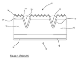
- a section of a standard prior art front contact laser grooved buried contact solar cell is illustrated and it generally comprises a semiconductor wafer 10 having a front surface 11 and a rear surface 12.
- the wafer material comprises a p-type base and a shallow n-type top layer. Initially the wafer is cleaned, usually chemically and then etched to remove any damage caused by sawing of the semiconductor material.
- the front surface 11 is then textured to produce an array 13 of random or irregular pyramid structures. This texturing enables any light which is not initially absorbed into the cell to be "trapped" so that it is not reflected off the surface 11.
- the wafer 10 is doped by diffusion therein of a suitable dopant to produce a p+-type doped region 18 at the base.
- the front surface 11 is provided with an antireflection coating 14 such as silicon nitride to further reduce reflection.
- Grooves 15 are formed by means of a laser through the antireflection coating 14 into the wafer at the front surface 11. The grooves 15 are usually etched to clean any excess fragments.
- the surface is again subject to diffusion to create an n+-type doped region 17. This diffusion is restricted by the nitride antireflective coating 14 to the regions that have been cut by the laser.
- An aluminium layer (not shown) is then evaporated onto the rear surface 12 of the wafer and then sintered.
- the front 11 and rear surfaces 12 are then electrolessly plated to form a nickel layer 19 followed by copper and silver which is deposited in order to form the contacts.
- the antireflective nitride coating 14 restricts the plating on the front surface to the grooves 15.
- the front contact of this section of the LGBC cell has two grooves 15.
- a number of grooves 15 are required on the cell surface 11 in order to achieve a high level of concentration.
- the metallization in the grooves 15 shades the surface 11 and reduces the efficiency of the solar cell by reflecting light away from the surface 11.
- Figure 2A to 2F illustrates the sequence of steps required in order to form the DGRC photovoltaic solar cell of Figure 3 and are in accordance with the method of the present invention.
- the semiconductor wafer 25 is cleaned and then textured by standard methods to form a pyramid structure 28 on the front surface 26.
- the wafer comprises a p-type layer 24 and a shallow n-type layer 23 at the front surface.
- the rear surface 27 is then doped by standard methods to produce a 100 ⁇ /square p ++ type doped region 29. This is accomplished by spinning on a suitable dopant source material and heating to approximately 1000°C in a belt furnace or quartz tube furnace until the desired 100 ⁇ /square diffusion is achieved.
- the dopant atoms disperse into the rear surface 27 of the wafer 25 by thermal diffusion. If the groove is produced by a method that includes a water jet, it is possible for the dopant to be applied to the second doped region by including it in the water of the jet. This can remove or reduce the need to heat the wafer, because the heat generated by the cutting can be enough to permit the introduction of the dopant from the water into the material of the wafer.
- passivation layers 30 are deposited on the front 26 and rear surface 27. This layer serves as an antireflection layer for the front surface 26, to prevent light being reflected away from the front surface 26.
- the passivation layer 30 also serves as a mask for the rear surface 27, which will be explained in more detail below.
- the passivation layers 30 also serve to reduce the recombination velocity of the electrons in the solar cell and are formulated to give a front 26 and rear 27 surface recombination velocity below 500 cm/s.
- Standard laser grooving or laser micro-jetting technologies using pulsed lasers are used to scribe deep laser grooves 31 in the rear surface 27, as shown in Figure 2C , for the rear contact.
- the grooves may be formed by other means.
- the grooves 15 are required to come within one diffusion length of the front surface 26 and adjacent grooves preferably need to be less than two diffusion lengths apart.
- the grooves of a typical Czochralski wafer of 200 ⁇ m thickness should be approximately 150 ⁇ m deep and separated by approximately 300 ⁇ m.
- These grooves 31 are etched to remove any surplus wafer particles and the rear surface 27 is then doped again to produce an n ++ second doped region 32.
- the doping may be with phosphorus using standard techniques.
- the passivation layer 30 applied to the rear surface 27 acts as a mask such that during this second doping process the permeation into the wafer occurs only in the grooves 31.
- the diffusion into the material around the grooves 31 should be to a junction depth to give a sheet resistance of less than 10 ⁇ /square.
- a via 33 is then opened through the rear surface passivation layer 30 to allow contact to the p++ doped region 29 of the rear surface 27. This is achieved by laser scribing the passivation layer 30.
- Figure 2E illustrates the standard plating sequence used in the standard solar cell of Figure 1 .
- Nickel is electrolessly deposited on the rear surface 27 and it is then sintered, followed by electroless copper deposition.
- Silver is then passivated on the copper surface. This process fills the vias 33 to form p-type contacts 38 and fills the grooves 31 to form the n-type contacts 37.
- the rear surface 27 is then scribed or etched to form breaks 35 that isolate the electrical contacts 37 from the p-type contacts 38. This isolation scribe step is accomplished using standard technology.
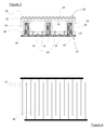
- the photovoltaic solar cell of the present invention formed by the method above can be seen in Figure 3 .
- the wafer 25 comprises a p-type layer 24 adjacent a rear surface 27 and a shallow n-type layer 23 at a front surface 26.
- the front surface 26 is textured to give a pyramid style structure 28 which reduces reflection of the incoming light.
- the rear surface 27 of the wafer 25 is doped with boron to produce a first p + doped region 29.
- the boron dopant seeps into the cell surface 27 by thermal diffusion.
- the front 26 and rear surfaces 27 have an antireflection passivation layer 30 thereon.
- Grooves are formed in the rear surface 27 through the passivation layer 30 and a second doped region 32 is formed around the grooves by doping with phosphorus to produce an n + doped region.
- the grooves 31 are filled with nickel, copper and silver to provide the n-type electrical contacts 37.
- P-type electrical contacts 38 are also formed from nickel, copper and silver deposited into shallow channels cut through the rear passivation layer. These contacts 37 38 are isolated from each other by breaks scribed onto the rear surface after the deposition of the metal material.
- Figure 4 illustrates a schematic representation of the rear surface 27 of the solar cell illustrated in Figure 3 . As shown, the n-type contact 37 is isolated from the p-type contact 38. The contacts of each type are linked together.
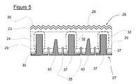
- Figure 5 shows a second embodiment of photovoltaic concentrator solar cell that is similar to that described above with like parts given like reference numerals.
- the p-type contacts 40 are much larger than those described above.
- the vias formed pass not only through the rear passivation layer 30 but deep into (and possible all the way through) the first p ++ doped region 29. In fact such vias are more in the form of second grooves, which like the first grooves may be further doped during or after formation.
- the larger area of the p-type contacts reduces the both contact and series resistance.
Claims (9)
- Méthode de formation de cellules solaires de concentrateur photovoltaïque à partir d'une plaquette à semi-conducteur (25) ayant une surface avant (26) et une surface arrière (27) comprenant les étapes suivantes :(a) dopage de la surface arrière (27) de ladite plaquette (25) de façon à fournir une première région dopée (29) à l'arrière de ladite plaquette (25) ;(b) dépôt de couches de passivation (30) sur la surface avant et arrière (26, 27) pour fournir un masque dopant ;(c) formation d'une ou plusieurs rainures (31) dans la surface arrière (27), à travers la couche de passivation (30), dans une longueur de diffusion de la surface avant (26) de la plaquette (25) ;(d) dopage de ladite surface arrière (27) de façon à fournir une seconde région dopée (32) uniquement dans la ou les rainures (31), ladite seconde région dopée (32) étant dopée de manière opposée à ladite première région dopée (29), les couches de passivation (30) agissant comme un masque pour confiner la diffusion au sein de la plaquette (25) jusqu'à la zone des rainures uniquement ;(e) formation d'une ouverture (33) à travers la couche arrière de passivation (30) jusqu'à la première région dopée (29) ; et(f) formation de contacts électriques (37, 38) sur ladite surface arrière (27) pour se connecter électriquement à la première et la seconde régions dopées (29, 32).
- Méthode selon la revendication 1, dans laquelle les contacts électriques (37, 38) de la première et la seconde régions dopées (29, 32) sont isolés électriquement en gravant la surface arrière (27).
- Méthode selon la revendication 1 ou 2, dans laquelle les contacts électriques (37, 38) sont formés à l'étape (f) par un dépôt sans courant comprenant une ou plusieurs étapes suivantes :(i) dépôt sans courant de nickel ;(ii) frittage sans courant de nickel ;(iii) dépôt sans courant de cuivre ; et(iv) passivation à l'argent d'une surface de cuivre.
- Méthode selon l'une des revendications précédentes, dans laquelle le dopage de la surface arrière (27) à l'étape (a) est effectué en appliquant un matériau de source dopant et en chauffant la plaquette (25) à approximativement 1000°C aux moyens d'un four à courroie ou d'un four à tube de quartz.
- Méthode selon la revendication 4, dans laquelle la chaleur est maintenue durant le temps requis pour produire une diffusion de 100Ω/carré.
- Méthode selon l'une des revendications précédentes, dans laquelle les couches de passivation (30) déposées à l'étape (b) donnent une vitesse de recombinaison des surfaces avant et arrière inférieure à 500cm/s.
- Méthode selon l'une des revendications précédentes, dans laquelle une pluralité de rainures (31) sont formées dans la surface arrière (27) et les rainures sont séparées de manière égale les unes des autres à moins de deux longueurs de diffusion.
- Méthode selon l'une des revendications précédentes, dans laquelle dans l'étape (d), la diffusion du dopant dans la ou les rainures (31) est à une profondeur de jonction suffisante pour fournir une résistance de surface de moins de 10Ω/carré.
- Méthode selon l'une des revendications précédentes, dans laquelle une pluralité d'ouvertures allongées (33) sont formées à travers la surface arrière (27) entre les rainures (31).
Applications Claiming Priority (2)
| Application Number | Priority Date | Filing Date | Title |
|---|---|---|---|
| GBGB0820684.9A GB0820684D0 (en) | 2008-11-12 | 2008-11-12 | Photovoltaic solar cells |
| PCT/GB2009/051528 WO2010055346A2 (fr) | 2008-11-12 | 2009-11-12 | Cellules solaires photovoltaïques |
Publications (2)
| Publication Number | Publication Date |
|---|---|
| EP2356687A2 EP2356687A2 (fr) | 2011-08-17 |
| EP2356687B1 true EP2356687B1 (fr) | 2016-10-12 |
Family
ID=40139786
Family Applications (1)
| Application Number | Title | Priority Date | Filing Date |
|---|---|---|---|
| EP09771758.1A Active EP2356687B1 (fr) | 2008-11-12 | 2009-11-12 | Cellules solaires photovoltaïques à gorge profonde |
Country Status (7)
| Country | Link |
|---|---|
| US (1) | US8889462B2 (fr) |
| EP (1) | EP2356687B1 (fr) |
| JP (1) | JP5503668B2 (fr) |
| KR (1) | KR101561682B1 (fr) |
| CN (1) | CN102246324B (fr) |
| GB (2) | GB0820684D0 (fr) |
| WO (1) | WO2010055346A2 (fr) |
Families Citing this family (33)
| Publication number | Priority date | Publication date | Assignee | Title |
|---|---|---|---|---|
| WO2010062991A1 (fr) * | 2008-11-26 | 2010-06-03 | Microlink Devices, Inc. | Pile solaire dotée d'un orifice de surface inférieure permettant de s'engager avec la couche émettrice |
| US20110195542A1 (en) * | 2010-02-05 | 2011-08-11 | E-Chem Enterprise Corp. | Method of providing solar cell electrode by electroless plating and an activator used therein |
| JP2011210802A (ja) * | 2010-03-29 | 2011-10-20 | Napura:Kk | 太陽電池 |
| CN102637766B (zh) * | 2011-02-15 | 2014-04-30 | 上海凯世通半导体有限公司 | 太阳能晶片掺杂方法、掺杂晶片、太阳能电池及制作方法 |
| CN102569492B (zh) * | 2010-12-17 | 2014-11-05 | 上海凯世通半导体有限公司 | 太阳能晶片的掺杂方法以及掺杂晶片 |
| CN102569491B (zh) * | 2010-12-17 | 2014-07-23 | 上海凯世通半导体有限公司 | 太阳能晶片的掺杂方法以及掺杂晶片 |
| CN102637767B (zh) * | 2011-02-15 | 2015-03-18 | 上海凯世通半导体有限公司 | 太阳能电池的制作方法以及太阳能电池 |
| US9559228B2 (en) * | 2011-09-30 | 2017-01-31 | Sunpower Corporation | Solar cell with doped groove regions separated by ridges |
| US9269851B2 (en) * | 2011-11-15 | 2016-02-23 | Newsouth Innovations Pty Limited | Metal contact scheme for solar cells |
| CN104115277A (zh) * | 2011-12-13 | 2014-10-22 | 道康宁公司 | 光伏电池及其形成方法 |
| TWI470816B (zh) * | 2011-12-28 | 2015-01-21 | Au Optronics Corp | 太陽能電池 |
| CN103208557A (zh) * | 2012-01-13 | 2013-07-17 | 上海凯世通半导体有限公司 | 太阳能电池的制作方法及太阳能电池 |
| CN103325666A (zh) * | 2012-03-21 | 2013-09-25 | 苏州贝克微电子有限公司 | 半导体晶圆掺杂扩散技术 |
| CN102623564B (zh) * | 2012-03-30 | 2015-01-07 | 中山大学 | 一种具有激光开槽正面电极的晶体硅太阳电池的制作方法 |
| CN102738288A (zh) * | 2012-06-20 | 2012-10-17 | 常州天合光能有限公司 | 非晶硅钝化n型背接触电池及其制备方法 |
| CN102832270A (zh) * | 2012-08-16 | 2012-12-19 | 友达光电股份有限公司 | 太阳能电池及其制作方法 |
| CN102856328B (zh) * | 2012-10-10 | 2015-06-10 | 友达光电股份有限公司 | 太阳能电池及其制作方法 |
| CN102881737A (zh) * | 2012-10-15 | 2013-01-16 | 浙江正泰太阳能科技有限公司 | 体结背接触太阳能电池 |
| CN102903775B (zh) * | 2012-10-24 | 2014-10-22 | 中国科学院半导体研究所 | 用于聚光和激光输能的晶体硅太阳能电池结构及其制作方法 |
| WO2014137284A1 (fr) * | 2013-03-05 | 2014-09-12 | Trina Solar Energy Development Pte Ltd | Procédé de fabrication d'une cellule solaire |
| TW201442261A (zh) * | 2013-04-30 | 2014-11-01 | Terasolar Energy Materials Corp | 矽晶太陽能電池的製造方法以及矽晶太陽能電池 |
| CN103794679B (zh) * | 2014-01-26 | 2016-07-06 | 晶澳(扬州)太阳能科技有限公司 | 一种背接触太阳能电池的制备方法 |
| US20160284917A1 (en) * | 2015-03-27 | 2016-09-29 | Seung Bum Rim | Passivation Layer for Solar Cells |
| WO2017146214A1 (fr) * | 2016-02-26 | 2017-08-31 | 京セラ株式会社 | Élément de photopile |
| TWI668876B (zh) * | 2017-08-29 | 2019-08-11 | 柯作同 | 太陽能電池及其製造方法 |
| WO2019102073A1 (fr) * | 2017-11-24 | 2019-05-31 | Aalto-Korkeakoulusäätiö Sr | Structure semi-conductrice photovoltaïque |
| US11081606B2 (en) * | 2018-12-27 | 2021-08-03 | Solarpaint Ltd. | Flexible and rollable photovoltaic cell having enhanced properties of mechanical impact absorption |
| CN114695594A (zh) * | 2020-12-30 | 2022-07-01 | 苏州阿特斯阳光电力科技有限公司 | 背接触电池的制备方法及背接触电池 |
| CN113964223B (zh) * | 2021-10-15 | 2023-11-10 | 浙江大学 | 一种抑制切割边缘漏电的晶体硅太阳能电池片、电池组件及制备方法 |
| CN113964222B (zh) * | 2021-10-15 | 2023-11-10 | 浙江大学 | 一种低漏电的晶体硅太阳能电池片、电池组件及制备方法 |
| CN115000214B (zh) * | 2022-06-23 | 2024-03-29 | 浙江爱旭太阳能科技有限公司 | 一种p型太阳能电池及其制作方法、电池组件和光伏系统 |
| CN115084299A (zh) * | 2022-06-23 | 2022-09-20 | 浙江爱旭太阳能科技有限公司 | 一种p型太阳能电池及其制作方法、电池组件和光伏系统 |
| CN115000247B (zh) * | 2022-07-29 | 2022-11-04 | 中国华能集团清洁能源技术研究院有限公司 | 内部钝化的背接触perc电池片的制作方法 |
Family Cites Families (19)
| Publication number | Priority date | Publication date | Assignee | Title |
|---|---|---|---|---|
| US4703553A (en) * | 1986-06-16 | 1987-11-03 | Spectrolab, Inc. | Drive through doping process for manufacturing low back surface recombination solar cells |
| US4838952A (en) | 1988-04-29 | 1989-06-13 | Spectrolab, Inc. | Controlled reflectance solar cell |
| US5053083A (en) * | 1989-05-08 | 1991-10-01 | The Board Of Trustees Of The Leland Stanford Junior University | Bilevel contact solar cells |
| JPH0682854B2 (ja) * | 1989-11-24 | 1994-10-19 | 株式会社日立製作所 | 太陽電池 |
| KR100378343B1 (ko) | 1996-01-09 | 2003-07-18 | 삼성전자주식회사 | 후면 함몰전극형 태양전지 |
| JP2001267610A (ja) * | 2000-03-17 | 2001-09-28 | Hitachi Ltd | 太陽電池 |
| KR100372343B1 (ko) | 2000-12-22 | 2003-02-15 | 엘지전자 주식회사 | 넘버.세븐 신호망에서의 폐기 메시지 관리 방법 |
| US7217883B2 (en) * | 2001-11-26 | 2007-05-15 | Shell Solar Gmbh | Manufacturing a solar cell with backside contacts |
| US7169669B2 (en) * | 2001-12-04 | 2007-01-30 | Origin Energy Solar Pty. Ltd. | Method of making thin silicon sheets for solar cells |
| US7339110B1 (en) * | 2003-04-10 | 2008-03-04 | Sunpower Corporation | Solar cell and method of manufacture |
| JP2005310830A (ja) * | 2004-04-16 | 2005-11-04 | Sharp Corp | 太陽電池および太陽電池の製造方法 |
| CN1957478A (zh) * | 2004-04-30 | 2007-05-02 | 新南创新有限公司 | 人造无定形半导体及其在太阳能电池中的应用 |
| JP4641858B2 (ja) * | 2005-04-22 | 2011-03-02 | シャープ株式会社 | 太陽電池 |
| JP4481869B2 (ja) * | 2005-04-26 | 2010-06-16 | 信越半導体株式会社 | 太陽電池の製造方法及び太陽電池並びに半導体装置の製造方法 |
| JP2007059644A (ja) * | 2005-08-25 | 2007-03-08 | Toyota Motor Corp | 光起電力素子 |
| US20070137692A1 (en) * | 2005-12-16 | 2007-06-21 | Bp Corporation North America Inc. | Back-Contact Photovoltaic Cells |
| JP2009152222A (ja) * | 2006-10-27 | 2009-07-09 | Kyocera Corp | 太陽電池素子の製造方法 |
| CN101017858A (zh) * | 2007-01-10 | 2007-08-15 | 北京市太阳能研究所有限公司 | 一种背接触式太阳能电池及其制作方法 |
| CN201112399Y (zh) | 2007-09-27 | 2008-09-10 | 江苏林洋新能源有限公司 | 具有浓硼浓磷扩散结构的太阳能电池 |
-
2008
- 2008-11-12 GB GBGB0820684.9A patent/GB0820684D0/en not_active Ceased
-
2009
- 2009-11-12 WO PCT/GB2009/051528 patent/WO2010055346A2/fr active Application Filing
- 2009-11-12 EP EP09771758.1A patent/EP2356687B1/fr active Active
- 2009-11-12 KR KR1020117013407A patent/KR101561682B1/ko active IP Right Grant
- 2009-11-12 GB GB0919795.5A patent/GB2466342B/en active Active
- 2009-11-12 US US13/128,742 patent/US8889462B2/en active Active
- 2009-11-12 CN CN200980149558.3A patent/CN102246324B/zh active Active
- 2009-11-12 JP JP2011543814A patent/JP5503668B2/ja active Active
Also Published As
| Publication number | Publication date |
|---|---|
| KR101561682B1 (ko) | 2015-10-20 |
| JP2012508473A (ja) | 2012-04-05 |
| WO2010055346A2 (fr) | 2010-05-20 |
| EP2356687A2 (fr) | 2011-08-17 |
| WO2010055346A3 (fr) | 2011-03-31 |
| GB2466342B (en) | 2013-07-17 |
| CN102246324A (zh) | 2011-11-16 |
| US20110214721A1 (en) | 2011-09-08 |
| KR20110097827A (ko) | 2011-08-31 |
| CN102246324B (zh) | 2015-07-29 |
| JP5503668B2 (ja) | 2014-05-28 |
| GB0820684D0 (en) | 2008-12-17 |
| US8889462B2 (en) | 2014-11-18 |
| GB2466342A (en) | 2010-06-23 |
| GB0919795D0 (en) | 2009-12-30 |
Similar Documents
| Publication | Publication Date | Title |
|---|---|---|
| EP2356687B1 (fr) | Cellules solaires photovoltaïques à gorge profonde | |
| US8637340B2 (en) | Patterning of silicon oxide layers using pulsed laser ablation | |
| US5449626A (en) | Method for manufacture of a solar cell | |
| US9455362B2 (en) | Laser irradiation aluminum doping for monocrystalline silicon substrates | |
| US20070295399A1 (en) | Back-Contact Photovoltaic Cells | |
| US20070137692A1 (en) | Back-Contact Photovoltaic Cells | |
| US9705017B2 (en) | Nanostructured silicon based solar cells and methods to produce nanostructured silicon based solar cells | |
| US20100229928A1 (en) | Back-contact photovoltaic cell comprising a thin lamina having a superstrate receiver element | |
| US20120225515A1 (en) | Laser doping techniques for high-efficiency crystalline semiconductor solar cells | |
| EP3297038B1 (fr) | Cellule solaire | |
| US20130130430A1 (en) | Spatially selective laser annealing applications in high-efficiency solar cells | |
| US20100193016A1 (en) | Photovoltaic Cell and Production Thereof | |
| US20050189013A1 (en) | Process for manufacturing photovoltaic cells | |
| US20130164883A1 (en) | Laser annealing applications in high-efficiency solar cells | |
| KR20130052627A (ko) | 선택적 전면 필드를 구비한 후면 접합 태양전지 | |
| KR101072543B1 (ko) | 태양 전지의 제조 방법 | |
| US7858430B2 (en) | Method for making a photovoltaic cell comprising contact regions doped through a lamina | |
| US20170005206A1 (en) | Patterning of silicon oxide layers using pulsed laser ablation | |
| KR101396027B1 (ko) | 고효율 후면 접촉 후면 접합 태양 전지의 이온 주입 및 어닐링 | |
| US20100154873A1 (en) | Photovoltaic cell comprising ccontact regions doped through lamina | |
| KR101199649B1 (ko) | 국부화 에미터 태양전지 및 그 제조 방법 | |
| KR20110060130A (ko) | 태양전지 제조 시의 선택적 에미터 형성 방법 | |
| KR101114198B1 (ko) | 국부화 에미터 태양전지 및 그 제조 방법 | |
| KR101103144B1 (ko) | 후면전극형 태양전지 제조 방법 | |
| KR20120077708A (ko) | 국부화 에미터 태양전지 및 그 제조 방법 |
Legal Events
| Date | Code | Title | Description |
|---|---|---|---|
| PUAI | Public reference made under article 153(3) epc to a published international application that has entered the european phase |
Free format text: ORIGINAL CODE: 0009012 |
|
| 17P | Request for examination filed |
Effective date: 20110606 |
|
| AK | Designated contracting states |
Kind code of ref document: A2 Designated state(s): AT BE BG CH CY CZ DE DK EE ES FI FR GB GR HR HU IE IS IT LI LT LU LV MC MK MT NL NO PL PT RO SE SI SK SM TR |
|
| RIC1 | Information provided on ipc code assigned before grant |
Ipc: H01L 31/068 20060101ALI20111019BHEP Ipc: H01L 31/18 20060101AFI20111019BHEP |
|
| DAX | Request for extension of the european patent (deleted) | ||
| 17Q | First examination report despatched |
Effective date: 20140828 |
|
| REG | Reference to a national code |
Ref country code: DE Ref legal event code: R079 Ref document number: 602009041705 Country of ref document: DE Free format text: PREVIOUS MAIN CLASS: H01L0031023600 Ipc: H01L0031022400 |
|
| GRAP | Despatch of communication of intention to grant a patent |
Free format text: ORIGINAL CODE: EPIDOSNIGR1 |
|
| RIC1 | Information provided on ipc code assigned before grant |
Ipc: H01L 31/0352 20060101ALI20160413BHEP Ipc: H01L 31/0224 20060101AFI20160413BHEP Ipc: H01L 31/068 20120101ALI20160413BHEP Ipc: H01L 31/18 20060101ALI20160413BHEP |
|
| INTG | Intention to grant announced |
Effective date: 20160503 |
|
| GRAS | Grant fee paid |
Free format text: ORIGINAL CODE: EPIDOSNIGR3 |
|
| GRAA | (expected) grant |
Free format text: ORIGINAL CODE: 0009210 |
|
| AK | Designated contracting states |
Kind code of ref document: B1 Designated state(s): AT BE BG CH CY CZ DE DK EE ES FI FR GB GR HR HU IE IS IT LI LT LU LV MC MK MT NL NO PL PT RO SE SI SK SM TR |
|
| REG | Reference to a national code |
Ref country code: GB Ref legal event code: FG4D |
|
| REG | Reference to a national code |
Ref country code: CH Ref legal event code: EP |
|
| REG | Reference to a national code |
Ref country code: AT Ref legal event code: REF Ref document number: 837186 Country of ref document: AT Kind code of ref document: T Effective date: 20161015 |
|
| REG | Reference to a national code |
Ref country code: IE Ref legal event code: FG4D |
|
| REG | Reference to a national code |
Ref country code: DE Ref legal event code: R096 Ref document number: 602009041705 Country of ref document: DE |
|
| REG | Reference to a national code |
Ref country code: LT Ref legal event code: MG4D |
|
| REG | Reference to a national code |
Ref country code: NL Ref legal event code: MP Effective date: 20161012 |
|
| PG25 | Lapsed in a contracting state [announced via postgrant information from national office to epo] |
Ref country code: BE Free format text: LAPSE BECAUSE OF NON-PAYMENT OF DUE FEES Effective date: 20161130 Ref country code: LV Free format text: LAPSE BECAUSE OF FAILURE TO SUBMIT A TRANSLATION OF THE DESCRIPTION OR TO PAY THE FEE WITHIN THE PRESCRIBED TIME-LIMIT Effective date: 20161012 |
|
| REG | Reference to a national code |
Ref country code: AT Ref legal event code: MK05 Ref document number: 837186 Country of ref document: AT Kind code of ref document: T Effective date: 20161012 |
|
| PG25 | Lapsed in a contracting state [announced via postgrant information from national office to epo] |
Ref country code: SE Free format text: LAPSE BECAUSE OF FAILURE TO SUBMIT A TRANSLATION OF THE DESCRIPTION OR TO PAY THE FEE WITHIN THE PRESCRIBED TIME-LIMIT Effective date: 20161012 Ref country code: GR Free format text: LAPSE BECAUSE OF FAILURE TO SUBMIT A TRANSLATION OF THE DESCRIPTION OR TO PAY THE FEE WITHIN THE PRESCRIBED TIME-LIMIT Effective date: 20170113 Ref country code: LT Free format text: LAPSE BECAUSE OF FAILURE TO SUBMIT A TRANSLATION OF THE DESCRIPTION OR TO PAY THE FEE WITHIN THE PRESCRIBED TIME-LIMIT Effective date: 20161012 Ref country code: NO Free format text: LAPSE BECAUSE OF FAILURE TO SUBMIT A TRANSLATION OF THE DESCRIPTION OR TO PAY THE FEE WITHIN THE PRESCRIBED TIME-LIMIT Effective date: 20170112 |
|
| PG25 | Lapsed in a contracting state [announced via postgrant information from national office to epo] |
Ref country code: HR Free format text: LAPSE BECAUSE OF FAILURE TO SUBMIT A TRANSLATION OF THE DESCRIPTION OR TO PAY THE FEE WITHIN THE PRESCRIBED TIME-LIMIT Effective date: 20161012 Ref country code: PL Free format text: LAPSE BECAUSE OF FAILURE TO SUBMIT A TRANSLATION OF THE DESCRIPTION OR TO PAY THE FEE WITHIN THE PRESCRIBED TIME-LIMIT Effective date: 20161012 Ref country code: FI Free format text: LAPSE BECAUSE OF FAILURE TO SUBMIT A TRANSLATION OF THE DESCRIPTION OR TO PAY THE FEE WITHIN THE PRESCRIBED TIME-LIMIT Effective date: 20161012 Ref country code: ES Free format text: LAPSE BECAUSE OF FAILURE TO SUBMIT A TRANSLATION OF THE DESCRIPTION OR TO PAY THE FEE WITHIN THE PRESCRIBED TIME-LIMIT Effective date: 20161012 Ref country code: BE Free format text: LAPSE BECAUSE OF FAILURE TO SUBMIT A TRANSLATION OF THE DESCRIPTION OR TO PAY THE FEE WITHIN THE PRESCRIBED TIME-LIMIT Effective date: 20161012 Ref country code: AT Free format text: LAPSE BECAUSE OF FAILURE TO SUBMIT A TRANSLATION OF THE DESCRIPTION OR TO PAY THE FEE WITHIN THE PRESCRIBED TIME-LIMIT Effective date: 20161012 Ref country code: PT Free format text: LAPSE BECAUSE OF FAILURE TO SUBMIT A TRANSLATION OF THE DESCRIPTION OR TO PAY THE FEE WITHIN THE PRESCRIBED TIME-LIMIT Effective date: 20170213 Ref country code: NL Free format text: LAPSE BECAUSE OF FAILURE TO SUBMIT A TRANSLATION OF THE DESCRIPTION OR TO PAY THE FEE WITHIN THE PRESCRIBED TIME-LIMIT Effective date: 20161012 Ref country code: IS Free format text: LAPSE BECAUSE OF FAILURE TO SUBMIT A TRANSLATION OF THE DESCRIPTION OR TO PAY THE FEE WITHIN THE PRESCRIBED TIME-LIMIT Effective date: 20170212 |
|
| REG | Reference to a national code |
Ref country code: CH Ref legal event code: PL |
|
| REG | Reference to a national code |
Ref country code: DE Ref legal event code: R097 Ref document number: 602009041705 Country of ref document: DE |
|
| PG25 | Lapsed in a contracting state [announced via postgrant information from national office to epo] |
Ref country code: LI Free format text: LAPSE BECAUSE OF NON-PAYMENT OF DUE FEES Effective date: 20161130 Ref country code: CH Free format text: LAPSE BECAUSE OF NON-PAYMENT OF DUE FEES Effective date: 20161130 Ref country code: RO Free format text: LAPSE BECAUSE OF FAILURE TO SUBMIT A TRANSLATION OF THE DESCRIPTION OR TO PAY THE FEE WITHIN THE PRESCRIBED TIME-LIMIT Effective date: 20161012 Ref country code: DK Free format text: LAPSE BECAUSE OF FAILURE TO SUBMIT A TRANSLATION OF THE DESCRIPTION OR TO PAY THE FEE WITHIN THE PRESCRIBED TIME-LIMIT Effective date: 20161012 Ref country code: SK Free format text: LAPSE BECAUSE OF FAILURE TO SUBMIT A TRANSLATION OF THE DESCRIPTION OR TO PAY THE FEE WITHIN THE PRESCRIBED TIME-LIMIT Effective date: 20161012 Ref country code: EE Free format text: LAPSE BECAUSE OF FAILURE TO SUBMIT A TRANSLATION OF THE DESCRIPTION OR TO PAY THE FEE WITHIN THE PRESCRIBED TIME-LIMIT Effective date: 20161012 Ref country code: MC Free format text: LAPSE BECAUSE OF FAILURE TO SUBMIT A TRANSLATION OF THE DESCRIPTION OR TO PAY THE FEE WITHIN THE PRESCRIBED TIME-LIMIT Effective date: 20161012 Ref country code: CZ Free format text: LAPSE BECAUSE OF FAILURE TO SUBMIT A TRANSLATION OF THE DESCRIPTION OR TO PAY THE FEE WITHIN THE PRESCRIBED TIME-LIMIT Effective date: 20161012 |
|
| PLBE | No opposition filed within time limit |
Free format text: ORIGINAL CODE: 0009261 |
|
| STAA | Information on the status of an ep patent application or granted ep patent |
Free format text: STATUS: NO OPPOSITION FILED WITHIN TIME LIMIT |
|
| REG | Reference to a national code |
Ref country code: IE Ref legal event code: MM4A |
|
| REG | Reference to a national code |
Ref country code: FR Ref legal event code: ST Effective date: 20170731 |
|
| PG25 | Lapsed in a contracting state [announced via postgrant information from national office to epo] |
Ref country code: SM Free format text: LAPSE BECAUSE OF FAILURE TO SUBMIT A TRANSLATION OF THE DESCRIPTION OR TO PAY THE FEE WITHIN THE PRESCRIBED TIME-LIMIT Effective date: 20161012 Ref country code: IT Free format text: LAPSE BECAUSE OF FAILURE TO SUBMIT A TRANSLATION OF THE DESCRIPTION OR TO PAY THE FEE WITHIN THE PRESCRIBED TIME-LIMIT Effective date: 20161012 Ref country code: BG Free format text: LAPSE BECAUSE OF FAILURE TO SUBMIT A TRANSLATION OF THE DESCRIPTION OR TO PAY THE FEE WITHIN THE PRESCRIBED TIME-LIMIT Effective date: 20170112 |
|
| 26N | No opposition filed |
Effective date: 20170713 |
|
| PG25 | Lapsed in a contracting state [announced via postgrant information from national office to epo] |
Ref country code: LU Free format text: LAPSE BECAUSE OF NON-PAYMENT OF DUE FEES Effective date: 20161130 |
|
| PG25 | Lapsed in a contracting state [announced via postgrant information from national office to epo] |
Ref country code: FR Free format text: LAPSE BECAUSE OF NON-PAYMENT OF DUE FEES Effective date: 20161212 |
|
| PG25 | Lapsed in a contracting state [announced via postgrant information from national office to epo] |
Ref country code: SI Free format text: LAPSE BECAUSE OF FAILURE TO SUBMIT A TRANSLATION OF THE DESCRIPTION OR TO PAY THE FEE WITHIN THE PRESCRIBED TIME-LIMIT Effective date: 20161012 Ref country code: IE Free format text: LAPSE BECAUSE OF NON-PAYMENT OF DUE FEES Effective date: 20161112 |
|
| PG25 | Lapsed in a contracting state [announced via postgrant information from national office to epo] |
Ref country code: HU Free format text: LAPSE BECAUSE OF FAILURE TO SUBMIT A TRANSLATION OF THE DESCRIPTION OR TO PAY THE FEE WITHIN THE PRESCRIBED TIME-LIMIT; INVALID AB INITIO Effective date: 20091112 Ref country code: CY Free format text: LAPSE BECAUSE OF FAILURE TO SUBMIT A TRANSLATION OF THE DESCRIPTION OR TO PAY THE FEE WITHIN THE PRESCRIBED TIME-LIMIT Effective date: 20161012 |
|
| PG25 | Lapsed in a contracting state [announced via postgrant information from national office to epo] |
Ref country code: MK Free format text: LAPSE BECAUSE OF FAILURE TO SUBMIT A TRANSLATION OF THE DESCRIPTION OR TO PAY THE FEE WITHIN THE PRESCRIBED TIME-LIMIT Effective date: 20161012 Ref country code: TR Free format text: LAPSE BECAUSE OF FAILURE TO SUBMIT A TRANSLATION OF THE DESCRIPTION OR TO PAY THE FEE WITHIN THE PRESCRIBED TIME-LIMIT Effective date: 20161012 |
|
| PG25 | Lapsed in a contracting state [announced via postgrant information from national office to epo] |
Ref country code: MT Free format text: LAPSE BECAUSE OF NON-PAYMENT OF DUE FEES Effective date: 20161112 |
|
| P01 | Opt-out of the competence of the unified patent court (upc) registered |
Effective date: 20230502 |
|
| PGFP | Annual fee paid to national office [announced via postgrant information from national office to epo] |
Ref country code: GB Payment date: 20230901 Year of fee payment: 15 |
|
| PGFP | Annual fee paid to national office [announced via postgrant information from national office to epo] |
Ref country code: DE Payment date: 20231120 Year of fee payment: 15 |