EP2356574B1 - Entdeckung von verbindungen unter verwendung eines steuerbusses - Google Patents
Entdeckung von verbindungen unter verwendung eines steuerbusses Download PDFInfo
- Publication number
- EP2356574B1 EP2356574B1 EP09744831A EP09744831A EP2356574B1 EP 2356574 B1 EP2356574 B1 EP 2356574B1 EP 09744831 A EP09744831 A EP 09744831A EP 09744831 A EP09744831 A EP 09744831A EP 2356574 B1 EP2356574 B1 EP 2356574B1
- Authority
- EP
- European Patent Office
- Prior art keywords
- state
- control bus
- source device
- sink
- bus
- Prior art date
- Legal status (The legal status is an assumption and is not a legal conclusion. Google has not performed a legal analysis and makes no representation as to the accuracy of the status listed.)
- Active
Links
- 230000007704 transition Effects 0.000 claims description 30
- 238000000034 method Methods 0.000 claims description 27
- 238000001514 detection method Methods 0.000 claims description 11
- 230000004044 response Effects 0.000 claims description 6
- 230000008878 coupling Effects 0.000 claims 2
- 238000010168 coupling process Methods 0.000 claims 2
- 238000005859 coupling reaction Methods 0.000 claims 2
- 230000007246 mechanism Effects 0.000 description 11
- 230000008569 process Effects 0.000 description 10
- 238000004590 computer program Methods 0.000 description 4
- 238000005516 engineering process Methods 0.000 description 4
- 230000006870 function Effects 0.000 description 4
- GJWAPAVRQYYSTK-UHFFFAOYSA-N [(dimethyl-$l^{3}-silanyl)amino]-dimethylsilicon Chemical compound C[Si](C)N[Si](C)C GJWAPAVRQYYSTK-UHFFFAOYSA-N 0.000 description 3
- 238000004891 communication Methods 0.000 description 2
- 238000010586 diagram Methods 0.000 description 2
- 230000003287 optical effect Effects 0.000 description 2
- 230000002093 peripheral effect Effects 0.000 description 2
- XUIMIQQOPSSXEZ-UHFFFAOYSA-N Silicon Chemical compound [Si] XUIMIQQOPSSXEZ-UHFFFAOYSA-N 0.000 description 1
- 230000004913 activation Effects 0.000 description 1
- 230000001413 cellular effect Effects 0.000 description 1
- 230000011664 signaling Effects 0.000 description 1
- 229910052710 silicon Inorganic materials 0.000 description 1
- 239000010703 silicon Substances 0.000 description 1
Images


Classifications
-
- G—PHYSICS
- G06—COMPUTING; CALCULATING OR COUNTING
- G06F—ELECTRIC DIGITAL DATA PROCESSING
- G06F13/00—Interconnection of, or transfer of information or other signals between, memories, input/output devices or central processing units
- G06F13/38—Information transfer, e.g. on bus
- G06F13/40—Bus structure
- G06F13/4004—Coupling between buses
- G06F13/4022—Coupling between buses using switching circuits, e.g. switching matrix, connection or expansion network
-
- G—PHYSICS
- G06—COMPUTING; CALCULATING OR COUNTING
- G06F—ELECTRIC DIGITAL DATA PROCESSING
- G06F13/00—Interconnection of, or transfer of information or other signals between, memories, input/output devices or central processing units
- G06F13/38—Information transfer, e.g. on bus
- G06F13/40—Bus structure
- G06F13/4063—Device-to-bus coupling
- G06F13/4068—Electrical coupling
- G06F13/4081—Live connection to bus, e.g. hot-plugging
Definitions
- Embodiments of the invention generally relate to the field of networks and, more particularly, to a method and apparatus for discovery of connections utilizing a control bus.
- entertainment and multi-media devices may be interconnected to transfer or share digital information.
- the connection of such devices generally requires some form of standard bus or interface to allow the devices to easily connect and communicate with each other.
- the HDMI TM High-Definition Multimedia Interface
- HDMI provides an interface that allows for the transfer of uncompressed digital high-definition video and audio, together with associated control signals.
- HDMI includes the High-Definition Multimedia Interface 1.4 (Hitachi, Ltd., Matsushita Electric Industrial Co., Ltd., Philips Consumer Electronics, International B.V., Silicon Image, Inc., Sony Corporation, Thomson Inc., and Toshiba Corporation) (May 28, 2009) and High-Definition Multimedia Interface 1.3 (June 22, 2006), as well as earlier and later versions of HDMI.
- Multimedia devices may include any devices capable of providing, storing, or displaying multimedia data, including television monitors, cable and satellite set-top boxes, video players, including DVD (Digital Versatile Disk), HD (High-Definition) DVD, and Blu-Ray players, audio players, digital video recorders, and other similar devices.
- HDMI devices utilize TMDS TM (Transition Minimized Differential Signaling) technology.
- TMDS encoding converts 8 bits per TMDS data channel into a 10-bit DC-balanced, transition minimized sequence, which is then transmitted serially across the pair at a rate of 10 bits per TMDS clock period.
- An HDMI connection may include a DDC (Display Data Channel) for configuration and status exchange between a source device and a sink device, and an optional CEC (Consumer Electronics Control) protocol to provide high-level control functions among audiovisual products in a user's environment.
- DDC Display Data Channel
- CEC Consumer Electronics Control
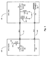
- Figure 1 illustrates an embodiment of detection of connections utilizing a control bus
- Figure 2 illustrates an embodiment of a connection sequence for source and sink devices
- Figure 3 illustrates an embodiment of a disconnection sequence for connected source and sink devices
- Figure 4 illustrates an embodiment of a source apparatus or system including a switch mechanism for establishing connections
- Figure 5 is a flow chart to illustrate an embodiment of discovery of a connection for a source element
- Figure 6 is a flow chart to illustrate an embodiment of discovery of a connection for a sink element
- Figure 7 is a flow chart to illustrate an embodiment of detection of a type of sink device connected to a source device or system.
- Figure 8 is a state transition diagram to illustrate an embodiment of a discovery sequence.
- Embodiments of the invention are generally directed to discovery of connections utilizing a control bus.
- an embodiment of a method includes detecting a transition of a control bus from a high state to a low state by a source device, the source device being configured to be coupled wth a sink device via an interface, the interface including the control bus, where the source device includes a pullup device and the sink device includes a pulldown device.
- the method further includes pulsing the control bus to a high state at the source device, and, upon detecting by the source device that the control bus remains in the high state, ceasing the pulsing of the control bus to the high state and transitioning the source device from a disconnected state to a connected state.
- an embodiment of method in a second aspect of the invention, includes pulling a control bus potential to a low state at a sink device by a pulldown device of the sink device, the sink device being configured to be coupled with a source device via an interface, where the interface includes the control bus and the source device includes a pullup device.
- the method further includes detecting a high state of the control bus at the sink device, disconnecting the pulldown device in response to the detection of the high state on the control bus by the sink device, and transitioning the sink device to a connected state.
- Embodiments of the invention are generally directed to discovery of connections utilizing a control bus.
- Mobile device means any mobile electronic device.
- the term “mobile device” includes, but is not limited to, a cellular telephone, smartphone, PDA (personal digital device), MP3 or other format music player, digital camera, video recorder, digital storage device, and other similar devices.
- a system provides an interface to connect a mobile device to other devices.
- a mobile device utilizes a modified protocol to allow connection with other devices, which devices may utilize a standard protocol.
- a standard device is a dual- or multiple-mode device that utilizes a control bus at least in part to discover what type of device is attached to the standard device.
- a system or method provides for detecting a connection between a sink device or element (which receives data) and a source device or element (which is a source of the data). In some embodiments, a system or method provides a means of distinguishing such connection from other possible connections to the source device.
- data being transferred between devices may be multimedia data and associated commands, including a stream of HDMI data and commands.
- a mobile device containing high-definition video data and related commands may be connected to a standard HDMI device (such as, for example, a television or a monitor).
- a standard HDMI device such as, for example, a television or a monitor.
- embodiments of the invention are not limited to any particular type of data or device.
- a device is a mobile device utilizing an MHLTM (Mobile High-Definition LinkTM) compatible connection.
- MHL protocol may utilize a 5 or 6 pin interface that carries audio, video, and auxiliary data between a source device and a sink device.
- separate mechanisms may be utilized on the source device and on the sink device to detect connectivity to each other.
- an interface may be presented via an MHL-specific connector or may be presented via standard connectors. Described below are a system and method of detecting connectivity to an MHL compatible sink device if the interface is an MHL-specific connector, and a system or method for distinguishing an MHL sink from other possible connections to a standard connector, which may include, but are not limited to, USBTM (Universal Serial Bus) compatible connectors such as micro-USB or mini-USB compatible connectors.
- USBTM Universal Serial Bus
- an MHL compatible interface may provide three signal pins (MHL+, MHL-, and control bus CBUS), a power pin (VBUS at +5V), and ground pins as provided in Table 1: Table 1 - Pin Connections PIN Signal Assignment 1 +5V (VBUS) 2 MHL- 3 MHL+ 4 CBUS 5 MHL GND Shell Power GND
- control bus provides a mechanism for a source device or a sink device to discover connectivity to an MHL-compliant sink device and source device, respectively.
- control bus is a single wire (one-bit), bi-directional control bus.
- a discovery system utilizes the control bus CBUS pin to detect a connection, and utilizes the voltage bus VBUS pin to detect a disconnection at the source.
- Figure 1 illustrates an embodiment of detection of connections utilizing a control bus.
- a control bus CBUS 115 and a power or voltage bus VBUS 120 are connected and provide an interface between an MHL compatible source device 105 and an MHL compatible sink device 110 in an MHL system. While the current illustration includes MHL technology, embodiments are not limited to this technology.
- the source device 105 pulls the CBUS 115 high because of a pullup device or element, illustrated here as a 10K ⁇ resistive pullup 125 connected to voltage source V CBUS 140.
- the sink device 110 pulls the CBUS 115 low due to a switched pulldown down device or element, illustrated as a 1K ⁇ termination 130 connected to a ground potential 140 switched by switch 170.
- the sink device 110 may further include a second pulldown device or element 135 with a larger impedance than the first pulldown device or element 130, illustrated as a 100K ⁇ resistive element also connected to ground potential.
- CBUS drivers 150 and 155 for the source device 105 and the sink device 110 respectively, to drive signals on the control bus 115.
- the VBUS 120 links a power source 160 via a switch 175 of the sink device with a VBUS level detection element or function of source device 165.
- source and sink devices may operate to discover connections, and may, for example, include an MHL compatible source and an MHL compatible sink discovering each other, such devices being connected by an MHL-specific connector or other standard connector.
- Figure 2 illustrates an embodiment of a connection sequence for source and sink devices.
- a source device such as source device 105 in Figure 1
- a sink device such as sink device 110 in Figure 1
- the MHL cable may include a control bus and a voltage bus (such as CBUS 115 and VBUS 120 illustrated in Figure 1 ).
- the CBUS transitions from a high state to a low state due to operation of a pulldown device or element, such as the 1K ⁇ sink device termination 130 of the sink device in Figure 1 .
- the source device detects this transition (A) and responds by repeatedly driving the CBUS high (B) and allowing the potential of the CBUS to float (C ⁇ D).
- the time period during which the source device floats the CBUS is the source device's "detection window".
- the sink device in turn detects the high value on the CBUS and responds (F) by turning off the 1K ⁇ sink termination, leaving on its 100K ⁇ pulldown (G).
- the sink device now transitions to an MHL-connected state.
- the source device detects that the CBUS stays high during its detection window, and stops pulsing the CBUS (E). The source now transitions to a connected state.
- the source device if the source device does not sense a high value on the CBUS during its detection window within a certain time after the source device commences pulsing the CBUS, the source device will stop pulsing and remain in a disconnected state. At this point, the source device will not attempt a re-discovery unless the source device detects another high-to-low transition on the CBUS.
- the devices are ready to begin communicating via the interface between the devices.
- the state of the VBUS is not defined prior to the sink entering the MHL-connected state (G).
- the sink device will drive VBUS to a high state (G ⁇ H) after the sink device transitions to an MHL-connected state.
- FIG 3 illustrates an embodiment of a disconnection sequence for connected source and sink devices.
- a source device such as source device 105 in Figure 1
- monitors the state of its VBUS pin (VBUS 120 and VBUS level detect 165) and transitions to a disconnected state whenever VBUS goes low for a certain time period (I ⁇ J).
- the sink device monitors the state of its CBUS pin and transitions to a disconnected state whenever CBUS goes low for longer than a particular time period, such as time period that normally occurs during CBUS communication (K ⁇ L).
- K ⁇ L time period that normally occurs during CBUS communication
- the sink device then turns off VBUS power (L ⁇ M) after transitioning to a disconnected state.
- devices may operate to discover connections, and may, for example, include an MHL compatible source utilizing an industry standard connector.
- MHL signals may be presented via a standard connector such as a micro-USB or mini-USB connector.
- a micro-USB connector is described as example.
- embodiments of the invention may include any type of connector.
- the USB protocol uses the ID signal as a means of discovering whether the USB device is operating as a host or as a peripheral.
- a number of USB accessories also use the USB ID signal as a means of identifying themselves to a USB device.
- a discovery mechanism for MHL protocol functions in this ecosystem to identify an MHL compatible sink and differentiate such elements from USB compatible devices or accessories.
- a source device may detect an existence and type of a sink device, and switch according to the type of sink device.
- an MHL device using a USB compatible connector conceptually includes an analog switch that can switch between MHL mode and USB mode, or other such switching mechanism.
- Figure 4 illustrates an embodiment of a source apparatus or system including a switch mechanism for establishing connections. Figure 4 provides an example of a mechanism using discrete chips. However, embodiments are not limited to any particular apparatus, and the function of the switch mechanism may be implemented using, for example, an integrated MHL transmitter and analog switch.
- a source device 405 includes an MHL transmitter 420 in an MHL subsystem of the source device 405.
- the MHL transmitter receives audio and video data from a baseband media processor 415, and the apparatus may provide either MHL mode data (a first mode) or USB mode data (a second mode) depending on the state or setting of an analog switch 425, which is then linked via a connector, illustrated as a micro-USB connector 435, to provide an interface with a sink device.
- power management module 410 Also illustrated is power management module 410.
- the CBUS from the MHL transmitter is mapped to pin 4 of the micro-USB connector, which is the pin that would carry the USB ID signal in USB mode operation.
- the USB ID pin is used to identify whether a USB device (host or peripheral) or accessory is connected to the micro-USB connector 435. This may be commonly done by measuring a resistance presented by the ID signal to the USB subsystem. A large range of possible ID resistances is in use, ranging from, for example, less than 10 ⁇ to over 100K ⁇ .
- a resistance of an MHL sink may be defined to be approximately 1 us2 when the sink element is in a disconnected state, which is a value that would fall within ranges of allowable ID impedances of a number of types of elements. For this reason, the identification of the resistance may not clearly identify a type of connected device.
- a discovery process is provided to unambiguously detect an MHL device under these conditions.
- the switch 425 is in USB mode by default.
- the switch 425 may include a pull-up element (not shown in Figure 4 ) of a high value, such as, for example, 1M ⁇ , on pin 4.
- the ID signal is at a logical high when the micro-USB connector is disconnected.
- a discovery sequence or mechanism is provided to allow for detecting an MHL device, including:
- transition of pin 4 to the logical low is used as a trigger to transition the switch 425 to MHL mode, in which the MHL subsystem (MHL transmitter 420, in this illustration) of the system 405 is selected to establish an MHL source.
- MHL subsystem MHL transmitter 420, in this illustration
- This transition to MHL mode exposes the CBUS for the MHL source to a logical low, allowing for the discovery process (as described above) to be carried out.
- the MHL source is queried to check for connectivity to an MHL sink via the connector 435.
- the switch 425 transitions to USB mode, allowing a usual USB device discovery process to commence. At this point the switch 425 enters a lockout period, during which the source 405 ignores any further transitions on pin 4.
- the switch 425 is locked to MHL mode if the MHL sink is in an MHL-discovered state.
- the switch is locked to USB mode if the USB subsystem indicates that it is connected to a USB device or accessory.
- the switch 425 transitions back to USB mode if the MHL sink indicates that it is in a disconnected state.
- FIG. 5 is a flow chart to illustrate an embodiment of discovery of a connection for a source element.
- a source device with a pullup element 502 may operate to detect connection with a second device, such as a sink device having a pulldown element, with the source device assumed to commence in an unconnected state 504.
- the source device will tend to pull a control bus CBUS high because of the operation of the pullup element 506.
- the source device if the source device detects that CBUS is in a low state 508, then the source device will commence pulsing the CBUS high and allowing the CBUS to float 510, the pulsing to provide a signal to a connected sink device to respond on the CBUS. In some embodiments, if the source device detects that the CBUS remains high 512, this is indicative of a sink device response, and the source device is transitioned to a connected state 518. In some embodiments, if the source device has not detected that the CBUS has remained high 512 and a detection window or time period has elapsed 514, then the source device ceases pulsing the CBUS and the source device remains in a disconnected state 516.
- the source device monitors a voltage bus VBUS for evidence of a disconnect 520. If the VBUS remains in a low state for a certain time period 522, this is indicative of the sink device being disconnected from the source device 524.
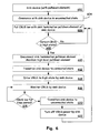
- FIG. 6 is a flow chart to illustrate an embodiment of discovery of a connection for a sink element.
- a sink device with a pulldown element 602 may operate to detect a connection with a second device, such as a source device having a pullup element, with the sink device assumed to begin in an unconnected state 604.
- the sink device will tend to pull a control bus CBUS low because of the operation of the pulldown element 606.
- the sink device includes a first pulldown element having a relatively small impedance value (which may be referred to as a sink termination element) that is switchable and a second pulldown element having a relatively high impedance value.
- the sink device if the sink device detects the CBUS in a high state 608, indicative of a source device pulsing the CBUS high, then the sink device disconnects the sink termination element, and maintains the second high value pulldown element 610. The sink device then transitions to a connected state 612, and drives a voltage bus VBUS high 614.
- the sink device monitors the CBUS 616. Upon detecting that the CBUS remains low for a certain time period 618, indicative of a disconnect from the source device, the sink device transitions to an unconnected state 620 and turns off the VBUS power 622.
- Figure 7 is a flow chart to illustrate an embodiment of detection of a type of sink device connected to a source device or system.
- a source device having multiple modes of operation 702 such as a first MHL mode and a second USB mode, may operate to detect a type of sink device connected to the source device.
- the source device operates to switch to an appropriate mode for the attached sink device.
- a source device defaults to the second mode, such as defaulting to a USB mode 703. If an impedance connected to the source device is consistent with a first mode device 704, such as an impedance of approximately 1K ohms for an MHL compatible device, a determination may be made whether the source device detects a certain pin is at a low state 706, such as pin 4 in Figure 4 , that is utilized for USB discovery in a USB mode and CBUS operation in MHL mode. If so, the source device switches to a first mode, such as switching to an MHL mode 710. If the connected impedance is not consistent with the first mode or a low state for the pin is not detected, the source device continues with operation in the second mode, such as standard USB discovery and operations 708.
- a first mode device 704 such as an impedance of approximately 1K ohms for an MHL compatible device
- the source device may proceed with a discovery sequence 712, such as the sequence illustrated in Figure 5 .
- a discovery sequence 712 such as the sequence illustrated in Figure 5 .
- the source device is queried with regard to whether the source device is connected with a first mode compatible sink device, such as an MHL compatible device 718. If so, the source device may continue to conduct communication operations in the first MHL mode 722. If the source device is not connected to a first mode compatible device, and thus the detected low state on the pin was not actually indicative of an MHL connection, then the source device may switch back the second USB mode 722. In some embodiments the source device may enter a lock out period during which state transitions on the pin are ignored.
- Figure 8 is a state transition diagram to illustrate an embodiment of a discovery sequence. This illustration specifically describes a USB connection, but the described mechanism is not limited to any particular connection, and may provide for discovery of MHL utilizing any other connectors.
- a system may include an MHL domain (a first mode domain), a USB domain (a second mode domain), and an auxiliary domain.
- a system may be in an idle or reset state with no cable connection 802.
- the system may transition to a USB-OTG (USB On-The-Go) mode 812, from which it may return to the idle state.
- USB-OTG USB On-The-Go
- VBUS state there is a determination whether on impedance on an ID pin is approximately 1K ⁇ , indicative of or consistent with an MHL device 804. If so, the system may proceed to a control bus check 806, including activation of the CBUS and request for MHL ID/status.
- the process includes a discovery sequence as described herein, such as the sequences illustrated in Figures 5 and 6 . If the check is successful, the system proceeds to operate in MHL mode 810.
- the connected impedance is not indicative of an MHL device 804 or the CBUS check 806 is not successful, there may be a determination whether a DN signal is pulled high 814. If so, there may be a carkit mode check and UART (universal asynchronous receiver/transmitter) mode request 816. If the UART request is granted 818, the system may continue with USB carkit operation 820. If DN is not pulled high 814 or UART is not granted 818, then there is a determination whether a DP signal is pulled high 822. If so, the system enters the USB-OTG mode, and if not the system enters an auxiliary mode.
- UART universal asynchronous receiver/transmitter
- Various embodiments of the present invention may include various processes. These processes may be performed by hardware components or may be embodied in computer program or machine-executable instructions, which may be used to cause a general-purpose or special-purpose processor or logic circuits programmed with the instructions to perform the processes. Alternatively, the processes may be performed by a combination of hardware and software.
- Portions of various embodiments of the present invention may be provided as a computer program product, which may include a computer-readable medium having stored thereon computer program instructions, which may be used to program a computer (or other electronic devices) to perform a process according to the embodiments of the present invention.
- the machine-readable medium may include, but is not limited to, floppy diskettes, optical disks, compact disk read-only memory (CD-ROM), and magneto-optical disks, read-only memory (ROM), random access memory (RAM), erasable programmable read-only memory (EPROM), electrically-erasable programmable read-only memory (EEPROM), magnet or optical cards, flash memory, or other type of media/machine-readable medium suitable for storing electronic instructions.
- the present invention may also be downloaded as a computer program product, wherein the program may be transferred from a remote computer to a requesting computer.
Claims (15)
- Verfahren, umfassend:das Detektieren des Übergangs eines Steuerbus von einem logischen Hochzustand in einen logischen Niedrigzustand durch eine Quellenvorrichtung, wobei die Quellenvorrichtung so konfiguriert ist, dass sie über eine Schnittstelle mit einer Senkenvorrichtung verbunden ist, wobei die Schnittstelle den Steuerbus umfasst, die Quellenvorrichtung eine Pullup-Vorrichtung umfasst und die Senkenvorrichtung eine Pulldown-Vorrichtung umfasst;das Pulsen des Steuerbus in einen logischen Hochzustand an der Quellenvorrichtung; undbeim Detektieren durch die Quellenvorrichtung, dass der Steuerbus im logischen Hochzustand bleibt:das Beenden des Pulsens des Steuerbus in den logischen Hochzustand unddas Überführen der Quellenvorrichtung von einem nichtverbundenen Zustand in einen verbundenen Zustand.
- Verfahren nach Anspruch 1, wobei der Steuerbus als Folge des Unterbrechens des verbundenen Zustands der Pulldown-Vorrichtung durch die Senkenvorrichtung in dem logischen Hochzustand verbleibt.
- Verfahren nach Anspruch 1, das weiters umfasst:das Detektieren des Übergangs eines Spannungsbus von einem logischen Hochzustand in einen logischen Niedrigzustand, wobei der Spannungsbus Teil der Schnittstelle zwischen der Quellenvorrichtung und der Senkenvorrichtung ist; unddas Überführen der Quellenvorrichtung vom verbundenen Zustand in den nichtverbundenen Zustand als Reaktion auf die Detektion des Übergangs des Spannungsbus in einen logischen Niedrigzustand.
- Verfahren nach Anspruch 1, das weiters umfasst:beim Übergang in den verbundenen Zustand das Abfragen der Konnektivität der Quellenvorrichtung mit der Senkenvorrichtung;wenn eine Konnektivität mit einer Senkenvorrichtung vorhanden ist, das Verbleiben im verbundenen Zustand; undwenn keine Konnektivität mit einer Senkenvorrichtung vorhanden ist, das Zurückkehren in den nichtverbundenen Zustand für eine Zeitdauer.
- Verfahren nach Anspruch 1, das weiters umfasst:wenn innerhalb eines bestimmten Zeitraums nach Beginn des Pulsens des Steuerbus kein logischer Hochzustand am Steuerbus erfasst wird:Beenden des Pulsens des Steuerbus; undHalten der Quellenvorrichtung im nichtverbundenen Zustand.
- Verfahren, umfassend:das Ziehen eines Steuerbuspotentials in einen logischen Niedrigzustand an einer Senkenvorrichtung mithilfe einer Pulldown-Vorrichtung der Senkenvorrichtung, wobei die Senkenvorrichtung so konfiguriert ist, dass sie über eine Schnittstelle mit der Quellenvorrichtung verbunden ist, wobei die Schnittstelle den Steuerbus umfasst, wobei die Quellenvorrichtung eine Pullup-Vorrichtung umfasst;das Detektieren eines logischen Hochzustands des Steuerbus an der Senkenvorrichtung;das Trennen des Verbindungszustands mit der Pulldown-Vorrichtung als Reaktion auf die Detektion des logischen Hochzustands am Steuerbus durch die Quellenvorrichtung; unddas Überführen der Senkenvorrichtung in einen verbundenen Zustand,wobei der detektierte logische Hochzustand des Steuerbus die Folge eines Pulsens des Steuerbus in einen logischen Hochzustand durch die Quellenvorrichtung ist.
- Verfahren nach Anspruch 6, das weiters umfasst:das Detektieren des Steuerbusübergangs in einen Niedrigzustand durch die Senkenvorrichtung und das Verbleiben im logischen Niedrigzustand länger als über einen bestimmten Zeitraum;das Überführen vom verbundenen Zustand in den nichtverbundenen Zustand als Reaktion auf das Detektieren des Steuerbusübergangs in einen Niedrigzustand.
- Verfahren nach Anspruch 7, das weiters das Aktivieren einer Spannungsquelle für einen Spannungsbus, wenn in den verbundenen Zustand übergeführt wird, und das Deaktivieren der Spannungsquelle, wenn in den nichtverbundenen Zustand übergeführt wird, umfasst, wobei der Spannungsbus Teil der Schnittstelle zwischen der Senkenvorrichtung und der Quellenvorrichtung ist.
- Gerät, umfassend:eine Schnittstelle zur Verbindung mit einem zweiten Gerät, wobei die Schnittstelle einen Steuerbus umfasst;eine Pullup-Vorrichtung, die mit dem Steuerbus verbunden ist; undeinen Treiber, um ein Signal für den Steuerbus zu erzeugen;wobei das Gerät so konfiguriert ist, dass es einen Übergang des Steuerbus vom logischen Hochzustand in einen logischen Niedrigzustand detektiert, und der Treiber so konfiguriert ist, dass er die Steuerleitung in einen Hochzustand pulst; undwobei, wenn das Gerät detektiert, dass der Steuerbus im logischen Hochzustand verbleibt, der Treiber das Pulsen der Steuerleitung in den Hochzustand beendet und das Gerät von einem nichtverbundenen Zustand in einen verbundenen Zustand übergeht.
- Gerät nach Anspruch 9, wobei die Schnittstelle weiters einen Energiebus umfasst und das Gerät so konfiguriert ist, dass es vom verbundenen Zustand in den nichtverbundenen Zustand übergeht, wenn das Gerät detektiert, dass der Energiebus für einen bestimmten Zeitraum von einem logischen Hochzustand in einen logischen Niedrigzustand übergeht.
- Gerät nach Anspruch 9, wobei das Gerät eine Quellenvorrichtung ist und das zweite Gerät eine Senkenvorrichtung ist, wobei das Gerät einen Datenstrom für das zweite Gerät bereitstellt.
- Gerät, umfassend:eine Schnittstelle zur Verbindung mit einer zweiten Vorrichtung, wobei die Schnittstelle einen Steuerbus umfasst;eine erste Pulldown-Vorrichtung und eine zweite Pulldown-Vorrichtung, die mit dem Steuerbus verbunden sind, wobei die erste Pulldown-Vorrichtung schaltbar ist; undeinen Treiber, um ein Signal für den Steuerbus zu erzeugen;wobei das Gerät so konfiguriert ist, dass es detektiert, dass sich der Steuerbus in einem logischen Hochzustand befindet, und das Gerät als Reaktion darauf, dass sich der Steuerbus im logischen Hochzustand befindet, die erste Pulldown-Vorrichtung abschaltet und das Gerät in einen verbundenen Zustand überleitet, wobei der detektierte logische Hochzustand des Steuerbus das Ergebnis des Pulsens des Steuerbus in einen Hochzustand durch die zweite Vorrichtung ist.
- Gerät nach Anspruch 12, wobei die Schnittstelle weiters einen Energiebus umfasst und wobei das Gerät weiters so konfiguriert ist, dass es beim Übergang des Geräts in einen verbundenen Zustand eine Spannung am Steuerbus aktiviert.
- Gerät nach Anspruch 13, wobei das Gerät weiters so konfiguriert ist, dass es vom verbundenen Zustand in einen nichtverbundenen Zustand übergeht und die Spannung am Energiebus abschaltet, wenn es detektiert, dass der Steuerbus in einem logischen Niedrigzustand verbleibt.
- Gerät nach Anspruch 12, wobei das Gerät eine Senkenvorrichtung ist und das zweite Gerät eine Quellenvorrichtung ist, wobei das Gerät zum Empfangen von Daten vom zweiten Gerät dient.
Applications Claiming Priority (3)
| Application Number | Priority Date | Filing Date | Title |
|---|---|---|---|
| US10612008P | 2008-10-16 | 2008-10-16 | |
| US12/577,707 US8275914B2 (en) | 2008-10-16 | 2009-10-12 | Discovery of connections utilizing a control bus |
| PCT/US2009/060685 WO2010045363A2 (en) | 2008-10-16 | 2009-10-14 | Discovery of connections utilizing a control bus |
Publications (2)
| Publication Number | Publication Date |
|---|---|
| EP2356574A2 EP2356574A2 (de) | 2011-08-17 |
| EP2356574B1 true EP2356574B1 (de) | 2012-09-05 |
Family
ID=41404482
Family Applications (1)
| Application Number | Title | Priority Date | Filing Date |
|---|---|---|---|
| EP09744831A Active EP2356574B1 (de) | 2008-10-16 | 2009-10-14 | Entdeckung von verbindungen unter verwendung eines steuerbusses |
Country Status (7)
| Country | Link |
|---|---|
| US (1) | US8275914B2 (de) |
| EP (1) | EP2356574B1 (de) |
| JP (1) | JP5436565B2 (de) |
| KR (1) | KR101575322B1 (de) |
| CN (1) | CN102203755B (de) |
| TW (1) | TWI546677B (de) |
| WO (1) | WO2010045363A2 (de) |
Families Citing this family (59)
| Publication number | Priority date | Publication date | Assignee | Title |
|---|---|---|---|---|
| US9030976B2 (en) * | 2008-03-27 | 2015-05-12 | Silicon Image, Inc. | Bi-directional digital interface for video and audio (DIVA) |
| TWI460995B (zh) * | 2008-12-11 | 2014-11-11 | Silicon Image Inc | 視訊及音頻數位互動介面之電力傳輸系統 |
| US8674679B2 (en) | 2009-10-08 | 2014-03-18 | Qualcomm Incorporated | Power saving during a connection detection |
| EP2556648A4 (de) | 2010-01-12 | 2013-12-11 | Silicon Image Inc | Multimedia-usb-datentransfer über eine digitale interaktionsschnittstelle für video und audia (diiva) |
| US8583836B2 (en) * | 2010-02-03 | 2013-11-12 | Stmicroelectronics, Inc. | Packet-based digital display interface signal mapping to bi-directional serial interface signals |
| EP2385517A1 (de) * | 2010-05-05 | 2011-11-09 | NXP Semiconductors B.V. | System und Verfahren zum Betrieb einer elektronischen Vorrichtung mit einem HDMI-Anschluss, der zwischen einer HDMI-Quellenfunktion und einer HDMI-Sinkfunktion der elektronischen Vorrichtung gemeinsam verwendet wird |
| JP5671838B2 (ja) * | 2010-05-21 | 2015-02-18 | ソニー株式会社 | データ送信装置、データ受信装置、データ送信方法およびデータ受信方法 |
| US8484387B2 (en) * | 2010-06-30 | 2013-07-09 | Silicon Image, Inc. | Detection of cable connections for electronic devices |
| US8601173B2 (en) * | 2010-06-30 | 2013-12-03 | Silicon Image, Inc. | Detection of cable connections for electronic devices |
| US9015509B2 (en) * | 2011-02-07 | 2015-04-21 | Silicon Image, Inc. | Mechanism for low power standby mode control circuit |
| IN2012DE00409A (de) * | 2011-02-14 | 2015-06-05 | Nikon Corp | |
| US9232265B2 (en) * | 2011-03-31 | 2016-01-05 | Lattice Semiconductor Corporation | Method, apparatus and system for transitioning an audio/video device between a source mode and a sink mode |
| US8683087B2 (en) * | 2011-04-11 | 2014-03-25 | Fairchild Semiconductor Corporation | Mobile device auto detection apparatus and method |
| TWI447585B (zh) * | 2011-11-24 | 2014-08-01 | Lin Peng Fei | 具有連接主機與裝置的儲存裝置 |
| CN103138321B (zh) * | 2011-12-02 | 2015-03-18 | 华为终端有限公司 | 集成网络接口转换装置的充电器 |
| FR2984540B1 (fr) * | 2011-12-20 | 2014-01-31 | Thales Sa | Procede et dispositif de detection de la deconnexion d'un peripherique a un equipement |
| US8856420B2 (en) * | 2011-12-27 | 2014-10-07 | Intel Corporation | Multi-protocol I/O interconnect flow control |
| US8775713B2 (en) * | 2011-12-27 | 2014-07-08 | Intel Corporation | Multi-protocol tunneling over an I/O interconnect |
| KR102011834B1 (ko) * | 2012-01-06 | 2019-08-19 | 엘지전자 주식회사 | 디스플레이 장치 |
| US20130191568A1 (en) * | 2012-01-23 | 2013-07-25 | Qualcomm Incorporated | Operating m-phy based communications over universal serial bus (usb) interface, and related cables, connectors, systems and methods |
| US8782321B2 (en) | 2012-02-08 | 2014-07-15 | Intel Corporation | PCI express tunneling over a multi-protocol I/O interconnect |
| EP2817723B1 (de) * | 2012-02-21 | 2017-06-07 | ZIH Corp. | Leiterplattenschnittstelle mit option für elektrische konfiguration |
| US8880923B2 (en) | 2012-03-29 | 2014-11-04 | Intel Corporation | Link power management in an I/O interconnect |
| US8891216B2 (en) | 2012-04-25 | 2014-11-18 | Apple Inc. | Techniques for detecting removal of a connector |
| US8724281B2 (en) * | 2012-04-25 | 2014-05-13 | Apple Inc. | Techniques for detecting removal of a connector |
| AU2013200705B2 (en) * | 2012-04-25 | 2014-09-04 | Apple Inc. | Techniques for detecting removal of a connector |
| KR101969726B1 (ko) * | 2012-05-02 | 2019-04-17 | 삼성전자주식회사 | 범용 직렬 버스 호스트 식별 방법 및 그 전자 장치 |
| WO2013172662A1 (ko) * | 2012-05-15 | 2013-11-21 | 엘지전자(주) | Hdmi cec 성능 향상을 위한 시스템 및 그 제어 방법 |
| GB2502967A (en) * | 2012-06-11 | 2013-12-18 | Denso Corp | Method of checking the compatibility of a mobile device connector and a vehicle connectivity port |
| US9087163B2 (en) * | 2012-07-11 | 2015-07-21 | Silicon Image, Inc. | Transmission of multiple protocol data elements via an interface utilizing a data tunnel |
| CN102890666B (zh) * | 2012-07-13 | 2015-09-30 | 华为终端有限公司 | 一种共用接口的装置及其方法、移动通讯终端 |
| TWI506536B (zh) | 2013-01-10 | 2015-11-01 | Accton Technology Corp | 執行裝置及其堆疊方法與堆疊系統 |
| KR102048222B1 (ko) * | 2013-05-21 | 2019-11-25 | 삼성전자주식회사 | 통신 시스템에서 외부 장치를 인식하는 장치 및 방법 |
| WO2014207910A1 (ja) * | 2013-06-28 | 2014-12-31 | 株式会社 東芝 | テレビジョン装置、及びリモートコントローラ |
| US8959257B2 (en) * | 2013-07-09 | 2015-02-17 | Kabushiki Kaisha Toshiba | Information processing apparatus and information processing method |
| CN203326671U (zh) * | 2013-07-10 | 2013-12-04 | 向智勇 | 一种用于电子烟盒的控制电路 |
| US9800822B2 (en) * | 2013-07-22 | 2017-10-24 | Qualcomm Incorporated | Method and apparatus for resource utilization in a source device for wireless display |
| US9131335B2 (en) | 2013-08-22 | 2015-09-08 | Nokia Technologies Oy | Method, apparatus, and computer program product for management of connected devices, such as in a wireless docking environment |
| US9497787B2 (en) * | 2013-11-25 | 2016-11-15 | Nokia Technologies Oy | Method, apparatus, and computer program product for managing concurrent connections between wireless dockee devices in a wireless docking environment |
| US9507398B2 (en) * | 2014-02-28 | 2016-11-29 | Infineon Technologies Austria Ag | Communication over identification line |
| US9703729B2 (en) * | 2014-04-04 | 2017-07-11 | Lattice Semiconductor Corporation | Detecting the orientation of a multimedia link connected to a device |
| US9448606B2 (en) * | 2014-09-23 | 2016-09-20 | Broadcom Corporation | Adaptive power configuration for a MHL and HDMI combination multimedia device |
| CN105512073A (zh) | 2014-09-25 | 2016-04-20 | 中兴通讯股份有限公司 | 语音交互方法、装置及系统 |
| US10282340B2 (en) * | 2014-12-17 | 2019-05-07 | The Boeing Company | Pin-configurable internal bus termination system |
| CN106233271B (zh) * | 2014-12-25 | 2019-06-07 | 华为技术有限公司 | 一种usb otg设备的识别系统及装置 |
| US10073806B2 (en) | 2015-05-13 | 2018-09-11 | Qualcomm Incorporated | Apparatus and methods for providing a reconfigurable bidirectional front-end interface |
| US10423205B2 (en) * | 2015-07-29 | 2019-09-24 | Texas Instruments Incorporated | Voltage transition control for USB power delivery sources |
| CN105868130A (zh) * | 2015-12-08 | 2016-08-17 | 乐视移动智能信息技术(北京)有限公司 | 一种控制接口应用程序的方法及移动终端 |
| TWI584127B (zh) * | 2015-12-28 | 2017-05-21 | 慧榮科技股份有限公司 | 電子裝置 |
| US10515025B2 (en) * | 2016-08-08 | 2019-12-24 | Cirrus Logic, Inc. | Communication protocol adapter |
| ES2734999T3 (es) | 2016-12-12 | 2019-12-13 | Mrs Corp Inc | Componente de procesamiento electrónico enchufable modular y sistema de procesamiento distribuido formado a partir del mismo |
| CN106786887B (zh) * | 2016-12-23 | 2019-08-23 | 捷开通讯(深圳)有限公司 | 一种充电控制系统 |
| EP3367210A1 (de) * | 2017-02-24 | 2018-08-29 | Thomson Licensing | Verfahren zum betätigen einer vorrichtung sowie entsprechende vorrichtung, system, computerlesbares programmprodukt und computerlesbares speichermedium |
| US11029750B2 (en) * | 2017-06-29 | 2021-06-08 | Intel Corporation | Apparatus for universal serial bus 2.0 (USB2) combined high speed squelch and disconnect detection |
| US10712801B2 (en) | 2017-06-30 | 2020-07-14 | Intel Corporation | USB type-C power delivery management |
| US11442523B2 (en) * | 2017-09-01 | 2022-09-13 | Sony Corporation | Cable and connection device |
| US10956352B2 (en) * | 2018-05-29 | 2021-03-23 | Continental Automotive Systems, Inc. | Automatic location based addressing method for network participants in a serial bus system |
| CN110062185A (zh) * | 2019-04-19 | 2019-07-26 | 北京灵优智学科技有限公司 | 一种接口电路 |
| TWI806536B (zh) * | 2022-04-06 | 2023-06-21 | 瑞昱半導體股份有限公司 | 異常狀態偵測的處理電路、網路設備與處理方法 |
Family Cites Families (17)
| Publication number | Priority date | Publication date | Assignee | Title |
|---|---|---|---|---|
| JP2713109B2 (ja) * | 1993-07-21 | 1998-02-16 | 日本電気株式会社 | 入出力回路 |
| US5568525A (en) | 1993-08-19 | 1996-10-22 | International Business Machines Corporation | System and method for connection of multiple protocol terminals |
| KR100272671B1 (ko) * | 1998-03-09 | 2000-11-15 | 윤종용 | 데이터 트랜시버 및 그것을 갖는 버스 인터페이스 |
| US6718415B1 (en) * | 1999-05-14 | 2004-04-06 | Acqis Technology, Inc. | Computer system and method including console housing multiple computer modules having independent processing units, mass storage devices, and graphics controllers |
| JP2001067309A (ja) * | 1999-08-25 | 2001-03-16 | Toshiba Corp | データ処理装置およびそのバス制御方法 |
| US6593768B1 (en) * | 1999-11-18 | 2003-07-15 | Intel Corporation | Dual termination serial data bus with pull-up current source |
| US6501660B1 (en) * | 2001-06-22 | 2002-12-31 | Sun Microsystems, Inc. | Reliable card detection in a CPCI system |
| US7058827B2 (en) * | 2001-07-18 | 2006-06-06 | Intel Corporation | Power saving circuit has an input line coupled to an external host and a keeper to hold the line in a weakly held state |
| JP3382933B2 (ja) * | 2001-07-27 | 2003-03-04 | 沖電気工業株式会社 | インタフェース回路 |
| JP3722217B2 (ja) * | 2002-04-26 | 2005-11-30 | セイコーエプソン株式会社 | データ転送制御装置、電子機器及びデータ転送制御方法 |
| KR100618814B1 (ko) * | 2003-07-04 | 2006-08-31 | 삼성전자주식회사 | 다중 호스트 인터페이스를 지원하는 스마트 카드 겸용이동형 저장 장치 및 이에 대한 인터페이스 방법 |
| US7606947B2 (en) | 2004-09-07 | 2009-10-20 | Industrial Technology Research Institute | Removable electronic device and method thereof |
| US7268561B2 (en) * | 2004-09-20 | 2007-09-11 | Texas Instruments Incorporated | USB attach detection for USB 1.1 and USB OTG devices |
| JP4022892B2 (ja) * | 2004-09-30 | 2007-12-19 | 三菱電機株式会社 | 通信アダプタ |
| JP2007172574A (ja) * | 2005-11-25 | 2007-07-05 | Seiko Epson Corp | 集積回路装置及び電子機器 |
| US7711870B2 (en) * | 2008-02-06 | 2010-05-04 | Panasonic Corporation | Interface detecting circuit and interface detecting method |
| US7788428B2 (en) * | 2008-03-27 | 2010-08-31 | Sony Ericsson Mobile Communications Ab | Multiplex mobile high-definition link (MHL) and USB 3.0 |
-
2009
- 2009-10-12 US US12/577,707 patent/US8275914B2/en active Active
- 2009-10-14 CN CN200980142160.7A patent/CN102203755B/zh active Active
- 2009-10-14 KR KR1020117011017A patent/KR101575322B1/ko active IP Right Grant
- 2009-10-14 JP JP2011532218A patent/JP5436565B2/ja active Active
- 2009-10-14 WO PCT/US2009/060685 patent/WO2010045363A2/en active Application Filing
- 2009-10-14 EP EP09744831A patent/EP2356574B1/de active Active
- 2009-10-16 TW TW098135190A patent/TWI546677B/zh active
Also Published As
| Publication number | Publication date |
|---|---|
| KR20110084945A (ko) | 2011-07-26 |
| KR101575322B1 (ko) | 2015-12-07 |
| JP2012506096A (ja) | 2012-03-08 |
| US20100100200A1 (en) | 2010-04-22 |
| JP5436565B2 (ja) | 2014-03-05 |
| WO2010045363A2 (en) | 2010-04-22 |
| EP2356574A2 (de) | 2011-08-17 |
| US8275914B2 (en) | 2012-09-25 |
| WO2010045363A3 (en) | 2010-06-10 |
| CN102203755A (zh) | 2011-09-28 |
| TWI546677B (zh) | 2016-08-21 |
| TW201017431A (en) | 2010-05-01 |
| CN102203755B (zh) | 2016-05-11 |
Similar Documents
| Publication | Publication Date | Title |
|---|---|---|
| EP2356574B1 (de) | Entdeckung von verbindungen unter verwendung eines steuerbusses | |
| US7921231B2 (en) | Discovery of electronic devices utilizing a control bus | |
| US9329672B2 (en) | High-definition multimedia interface (HDMI) receiver apparatuses, HDMI systems using the same, and control methods therefor | |
| US8151018B2 (en) | Dual-mode data transfer of uncompressed multimedia contents or data communications | |
| US7673092B2 (en) | PCI Express interface | |
| JP5683696B2 (ja) | 電子デバイスに関するケーブル接続の検出 | |
| US7856520B2 (en) | Control bus for connection of electronic devices | |
| KR101811602B1 (ko) | 소스 모드와 싱크 모드 사이에서 오디오/비디오 디바이스를 전환하는 방법. 장치 및 시스템 | |
| EP1901176B1 (de) | Audiosystem und gemeinsames USB/UART-Kommunikationssystem dafür | |
| US20080084834A1 (en) | Multiplexed connection interface for multimedia serial data transmission | |
| US20090037622A1 (en) | Method and system for changing operation modes of an interface device | |
| JP6661342B2 (ja) | ポート接続回路、ポート接続制御方法、電子機器 | |
| US20150186303A1 (en) | Display System And Operation Optimization Method | |
| WO2022103998A1 (en) | A redriver capable of switching between linear and limited modes | |
| JP2009289124A (ja) | デバイス機器検出装置およびデバイス機器検出方法 |
Legal Events
| Date | Code | Title | Description |
|---|---|---|---|
| PUAI | Public reference made under article 153(3) epc to a published international application that has entered the european phase |
Free format text: ORIGINAL CODE: 0009012 |
|
| 17P | Request for examination filed |
Effective date: 20110506 |
|
| AK | Designated contracting states |
Kind code of ref document: A2 Designated state(s): AT BE BG CH CY CZ DE DK EE ES FI FR GB GR HR HU IE IS IT LI LT LU LV MC MK MT NL NO PL PT RO SE SI SK SM TR |
|
| DAX | Request for extension of the european patent (deleted) | ||
| GRAP | Despatch of communication of intention to grant a patent |
Free format text: ORIGINAL CODE: EPIDOSNIGR1 |
|
| GRAS | Grant fee paid |
Free format text: ORIGINAL CODE: EPIDOSNIGR3 |
|
| GRAA | (expected) grant |
Free format text: ORIGINAL CODE: 0009210 |
|
| AK | Designated contracting states |
Kind code of ref document: B1 Designated state(s): AT BE BG CH CY CZ DE DK EE ES FI FR GB GR HR HU IE IS IT LI LT LU LV MC MK MT NL NO PL PT RO SE SI SK SM TR |
|
| REG | Reference to a national code |
Ref country code: GB Ref legal event code: FG4D |
|
| REG | Reference to a national code |
Ref country code: CH Ref legal event code: EP |
|
| REG | Reference to a national code |
Ref country code: AT Ref legal event code: REF Ref document number: 574394 Country of ref document: AT Kind code of ref document: T Effective date: 20120915 |
|
| REG | Reference to a national code |
Ref country code: IE Ref legal event code: FG4D |
|
| REG | Reference to a national code |
Ref country code: DE Ref legal event code: R096 Ref document number: 602009009504 Country of ref document: DE Effective date: 20121031 |
|
| REG | Reference to a national code |
Ref country code: AT Ref legal event code: MK05 Ref document number: 574394 Country of ref document: AT Kind code of ref document: T Effective date: 20120905 |
|
| REG | Reference to a national code |
Ref country code: NL Ref legal event code: VDEP Effective date: 20120905 |
|
| PG25 | Lapsed in a contracting state [announced via postgrant information from national office to epo] |
Ref country code: LT Free format text: LAPSE BECAUSE OF FAILURE TO SUBMIT A TRANSLATION OF THE DESCRIPTION OR TO PAY THE FEE WITHIN THE PRESCRIBED TIME-LIMIT Effective date: 20120905 Ref country code: NO Free format text: LAPSE BECAUSE OF FAILURE TO SUBMIT A TRANSLATION OF THE DESCRIPTION OR TO PAY THE FEE WITHIN THE PRESCRIBED TIME-LIMIT Effective date: 20121205 Ref country code: AT Free format text: LAPSE BECAUSE OF FAILURE TO SUBMIT A TRANSLATION OF THE DESCRIPTION OR TO PAY THE FEE WITHIN THE PRESCRIBED TIME-LIMIT Effective date: 20120905 Ref country code: HR Free format text: LAPSE BECAUSE OF FAILURE TO SUBMIT A TRANSLATION OF THE DESCRIPTION OR TO PAY THE FEE WITHIN THE PRESCRIBED TIME-LIMIT Effective date: 20120905 Ref country code: FI Free format text: LAPSE BECAUSE OF FAILURE TO SUBMIT A TRANSLATION OF THE DESCRIPTION OR TO PAY THE FEE WITHIN THE PRESCRIBED TIME-LIMIT Effective date: 20120905 |
|
| REG | Reference to a national code |
Ref country code: LT Ref legal event code: MG4D Effective date: 20120905 |
|
| PG25 | Lapsed in a contracting state [announced via postgrant information from national office to epo] |
Ref country code: LV Free format text: LAPSE BECAUSE OF FAILURE TO SUBMIT A TRANSLATION OF THE DESCRIPTION OR TO PAY THE FEE WITHIN THE PRESCRIBED TIME-LIMIT Effective date: 20120905 Ref country code: GR Free format text: LAPSE BECAUSE OF FAILURE TO SUBMIT A TRANSLATION OF THE DESCRIPTION OR TO PAY THE FEE WITHIN THE PRESCRIBED TIME-LIMIT Effective date: 20121206 Ref country code: SE Free format text: LAPSE BECAUSE OF FAILURE TO SUBMIT A TRANSLATION OF THE DESCRIPTION OR TO PAY THE FEE WITHIN THE PRESCRIBED TIME-LIMIT Effective date: 20120905 Ref country code: SI Free format text: LAPSE BECAUSE OF FAILURE TO SUBMIT A TRANSLATION OF THE DESCRIPTION OR TO PAY THE FEE WITHIN THE PRESCRIBED TIME-LIMIT Effective date: 20120905 |
|
| PG25 | Lapsed in a contracting state [announced via postgrant information from national office to epo] |
Ref country code: BE Free format text: LAPSE BECAUSE OF FAILURE TO SUBMIT A TRANSLATION OF THE DESCRIPTION OR TO PAY THE FEE WITHIN THE PRESCRIBED TIME-LIMIT Effective date: 20120905 Ref country code: IS Free format text: LAPSE BECAUSE OF FAILURE TO SUBMIT A TRANSLATION OF THE DESCRIPTION OR TO PAY THE FEE WITHIN THE PRESCRIBED TIME-LIMIT Effective date: 20130105 Ref country code: EE Free format text: LAPSE BECAUSE OF FAILURE TO SUBMIT A TRANSLATION OF THE DESCRIPTION OR TO PAY THE FEE WITHIN THE PRESCRIBED TIME-LIMIT Effective date: 20120905 Ref country code: CZ Free format text: LAPSE BECAUSE OF FAILURE TO SUBMIT A TRANSLATION OF THE DESCRIPTION OR TO PAY THE FEE WITHIN THE PRESCRIBED TIME-LIMIT Effective date: 20120905 Ref country code: RO Free format text: LAPSE BECAUSE OF FAILURE TO SUBMIT A TRANSLATION OF THE DESCRIPTION OR TO PAY THE FEE WITHIN THE PRESCRIBED TIME-LIMIT Effective date: 20120905 Ref country code: NL Free format text: LAPSE BECAUSE OF FAILURE TO SUBMIT A TRANSLATION OF THE DESCRIPTION OR TO PAY THE FEE WITHIN THE PRESCRIBED TIME-LIMIT Effective date: 20120905 |
|
| PG25 | Lapsed in a contracting state [announced via postgrant information from national office to epo] |
Ref country code: PT Free format text: LAPSE BECAUSE OF FAILURE TO SUBMIT A TRANSLATION OF THE DESCRIPTION OR TO PAY THE FEE WITHIN THE PRESCRIBED TIME-LIMIT Effective date: 20130107 Ref country code: PL Free format text: LAPSE BECAUSE OF FAILURE TO SUBMIT A TRANSLATION OF THE DESCRIPTION OR TO PAY THE FEE WITHIN THE PRESCRIBED TIME-LIMIT Effective date: 20120905 Ref country code: SK Free format text: LAPSE BECAUSE OF FAILURE TO SUBMIT A TRANSLATION OF THE DESCRIPTION OR TO PAY THE FEE WITHIN THE PRESCRIBED TIME-LIMIT Effective date: 20120905 Ref country code: MC Free format text: LAPSE BECAUSE OF NON-PAYMENT OF DUE FEES Effective date: 20121031 |
|
| PLBE | No opposition filed within time limit |
Free format text: ORIGINAL CODE: 0009261 |
|
| STAA | Information on the status of an ep patent application or granted ep patent |
Free format text: STATUS: NO OPPOSITION FILED WITHIN TIME LIMIT |
|
| REG | Reference to a national code |
Ref country code: IE Ref legal event code: MM4A |
|
| PG25 | Lapsed in a contracting state [announced via postgrant information from national office to epo] |
Ref country code: IE Free format text: LAPSE BECAUSE OF NON-PAYMENT OF DUE FEES Effective date: 20121014 Ref country code: BG Free format text: LAPSE BECAUSE OF FAILURE TO SUBMIT A TRANSLATION OF THE DESCRIPTION OR TO PAY THE FEE WITHIN THE PRESCRIBED TIME-LIMIT Effective date: 20121205 Ref country code: DK Free format text: LAPSE BECAUSE OF FAILURE TO SUBMIT A TRANSLATION OF THE DESCRIPTION OR TO PAY THE FEE WITHIN THE PRESCRIBED TIME-LIMIT Effective date: 20120905 |
|
| 26N | No opposition filed |
Effective date: 20130606 |
|
| PG25 | Lapsed in a contracting state [announced via postgrant information from national office to epo] |
Ref country code: IT Free format text: LAPSE BECAUSE OF FAILURE TO SUBMIT A TRANSLATION OF THE DESCRIPTION OR TO PAY THE FEE WITHIN THE PRESCRIBED TIME-LIMIT Effective date: 20120905 |
|
| REG | Reference to a national code |
Ref country code: DE Ref legal event code: R097 Ref document number: 602009009504 Country of ref document: DE Effective date: 20130606 |
|
| PG25 | Lapsed in a contracting state [announced via postgrant information from national office to epo] |
Ref country code: ES Free format text: LAPSE BECAUSE OF FAILURE TO SUBMIT A TRANSLATION OF THE DESCRIPTION OR TO PAY THE FEE WITHIN THE PRESCRIBED TIME-LIMIT Effective date: 20121216 |
|
| PG25 | Lapsed in a contracting state [announced via postgrant information from national office to epo] |
Ref country code: MT Free format text: LAPSE BECAUSE OF FAILURE TO SUBMIT A TRANSLATION OF THE DESCRIPTION OR TO PAY THE FEE WITHIN THE PRESCRIBED TIME-LIMIT Effective date: 20120905 Ref country code: CY Free format text: LAPSE BECAUSE OF FAILURE TO SUBMIT A TRANSLATION OF THE DESCRIPTION OR TO PAY THE FEE WITHIN THE PRESCRIBED TIME-LIMIT Effective date: 20120905 |
|
| PG25 | Lapsed in a contracting state [announced via postgrant information from national office to epo] |
Ref country code: TR Free format text: LAPSE BECAUSE OF FAILURE TO SUBMIT A TRANSLATION OF THE DESCRIPTION OR TO PAY THE FEE WITHIN THE PRESCRIBED TIME-LIMIT Effective date: 20120905 |
|
| PG25 | Lapsed in a contracting state [announced via postgrant information from national office to epo] |
Ref country code: SM Free format text: LAPSE BECAUSE OF FAILURE TO SUBMIT A TRANSLATION OF THE DESCRIPTION OR TO PAY THE FEE WITHIN THE PRESCRIBED TIME-LIMIT Effective date: 20120905 Ref country code: LU Free format text: LAPSE BECAUSE OF NON-PAYMENT OF DUE FEES Effective date: 20121014 |
|
| REG | Reference to a national code |
Ref country code: CH Ref legal event code: PL |
|
| PG25 | Lapsed in a contracting state [announced via postgrant information from national office to epo] |
Ref country code: HU Free format text: LAPSE BECAUSE OF FAILURE TO SUBMIT A TRANSLATION OF THE DESCRIPTION OR TO PAY THE FEE WITHIN THE PRESCRIBED TIME-LIMIT Effective date: 20091014 Ref country code: CH Free format text: LAPSE BECAUSE OF NON-PAYMENT OF DUE FEES Effective date: 20131031 Ref country code: LI Free format text: LAPSE BECAUSE OF NON-PAYMENT OF DUE FEES Effective date: 20131031 |
|
| PG25 | Lapsed in a contracting state [announced via postgrant information from national office to epo] |
Ref country code: MK Free format text: LAPSE BECAUSE OF FAILURE TO SUBMIT A TRANSLATION OF THE DESCRIPTION OR TO PAY THE FEE WITHIN THE PRESCRIBED TIME-LIMIT Effective date: 20120905 |
|
| REG | Reference to a national code |
Ref country code: FR Ref legal event code: PLFP Year of fee payment: 7 |
|
| REG | Reference to a national code |
Ref country code: FR Ref legal event code: PLFP Year of fee payment: 8 |
|
| REG | Reference to a national code |
Ref country code: FR Ref legal event code: PLFP Year of fee payment: 9 |
|
| REG | Reference to a national code |
Ref country code: FR Ref legal event code: PLFP Year of fee payment: 10 |
|
| REG | Reference to a national code |
Ref country code: DE Ref legal event code: R081 Ref document number: 602009009504 Country of ref document: DE Owner name: UNIVERSAL CONNECTIVITY TECHNOLOGIES, INC., WIL, US Free format text: FORMER OWNER: SILICON IMAGE, INC., SUNNYVALE, CALIF., US Ref country code: DE Ref legal event code: R081 Ref document number: 602009009504 Country of ref document: DE Owner name: LATTICE SEMICONDUCTOR CORP. (N. D. GES. D. STA, US Free format text: FORMER OWNER: SILICON IMAGE, INC., SUNNYVALE, CALIF., US |
|
| REG | Reference to a national code |
Ref country code: GB Ref legal event code: 732E Free format text: REGISTERED BETWEEN 20211104 AND 20211110 |
|
| REG | Reference to a national code |
Ref country code: DE Ref legal event code: R081 Ref document number: 602009009504 Country of ref document: DE Owner name: UNIVERSAL CONNECTIVITY TECHNOLOGIES, INC., WIL, US Free format text: FORMER OWNER: LATTICE SEMICONDUCTOR CORP. (N. D. GES. D. STAATES DELAWARE), HILLSBORO, OR, US |
|
| REG | Reference to a national code |
Ref country code: GB Ref legal event code: 732E Free format text: REGISTERED BETWEEN 20220623 AND 20220629 |
|
| P01 | Opt-out of the competence of the unified patent court (upc) registered |
Effective date: 20230411 |
|
| PGFP | Annual fee paid to national office [announced via postgrant information from national office to epo] |
Ref country code: GB Payment date: 20230831 Year of fee payment: 15 |
|
| PGFP | Annual fee paid to national office [announced via postgrant information from national office to epo] |
Ref country code: FR Payment date: 20230911 Year of fee payment: 15 |
|
| PGFP | Annual fee paid to national office [announced via postgrant information from national office to epo] |
Ref country code: DE Payment date: 20230830 Year of fee payment: 15 |