EP2348628A2 - Circuit de détection de synchronisation et appareil de parallélisation synchrone automatique - Google Patents
Circuit de détection de synchronisation et appareil de parallélisation synchrone automatique Download PDFInfo
- Publication number
- EP2348628A2 EP2348628A2 EP11152107A EP11152107A EP2348628A2 EP 2348628 A2 EP2348628 A2 EP 2348628A2 EP 11152107 A EP11152107 A EP 11152107A EP 11152107 A EP11152107 A EP 11152107A EP 2348628 A2 EP2348628 A2 EP 2348628A2
- Authority
- EP
- European Patent Office
- Prior art keywords
- voltage
- phase
- frequency
- value
- nts
- Prior art date
- Legal status (The legal status is an assumption and is not a legal conclusion. Google has not performed a legal analysis and makes no representation as to the accuracy of the status listed.)
- Granted
Links
Images


Classifications
-
- H—ELECTRICITY
- H02—GENERATION; CONVERSION OR DISTRIBUTION OF ELECTRIC POWER
- H02J—CIRCUIT ARRANGEMENTS OR SYSTEMS FOR SUPPLYING OR DISTRIBUTING ELECTRIC POWER; SYSTEMS FOR STORING ELECTRIC ENERGY
- H02J3/00—Circuit arrangements for ac mains or ac distribution networks
- H02J3/38—Arrangements for parallely feeding a single network by two or more generators, converters or transformers
- H02J3/40—Synchronising a generator for connection to a network or to another generator
- H02J3/42—Synchronising a generator for connection to a network or to another generator with automatic parallel connection when synchronisation is achieved
Definitions
- the present invention relates to a synchronization detecting circuit that detects a voltage amplitude of a single-phase AC voltage source as a synchronization target and a frequency difference and a phase difference between the single-phase AC voltage source and a voltage source on the synchronization detecting circuit side.
- the present invention relates to an automatic synchronous parallelization apparatus that adjusts a voltage amplitude, a frequency, and a phase of a single-phase voltage-type DC-to-AC converting device performing an autonomous parallel operation.
- a voltage is sampled for each predetermined period, and a change amount per one sample (corresponding to a differential value) and a change in the change amount (corresponding to a second-order differential) per one sample are calculated. Then, based on the derived values, the voltage amplitude, the frequency, and the phase are acquired, and then, differences thereof are calculated (for example, see Japanese Patent Application Laid-Open (JP-A) No. 52-40174 ).
- JP-A No. 09-028040 a technology for suppressing an inrush current at the time of connecting an inverter in parallel with a power system is known (for example, see JP-A No. 09-028040 ).
- JP-A No. 09-028040 a technology is disclosed in which a filter capacitor of an inverter is charged with a current having a phase led by 90 degrees from a voltage of the power system, and the inverter is connected in parallel with the power system after the voltage of the filter capacitor becomes the same as that of the power system.
- a single-phase voltage-type DC-to-AC converting device that performs an autonomous parallel operation by being connected in parallel with a single-phase voltage source such as a power system or a generator is known (for example, see JP-A No. 2009-219263 ).
- JP-A No. 2009-219263 a single-phase voltage-type DC-to-AC converting device that is operated by being coupled with an external single-phase AC voltage source by generating a single-phase AC voltage having a predetermined phase difference from the phase of the external single-phase AC voltage source and adjusting the amplitude, the frequency, and the phase of the generated single-phase AC voltage is disclosed.
- a sample voltage value is differentiated, and accordingly, there is a problem in that the influence of harmonic components included in a voltage waveform may be significant. Furthermore, division is used with an AC value being used as a denominator for detection of the frequency, and accordingly, there is a problem of instability in a case where a "division by zero" occurs.
- a synchronization detecting circuit that is not easily influenced by harmonic components and can reliably maintain stability.
- a single-phase voltage-type DC-to-AC converting device performing an autonomous parallel operation is controlled to be a voltage source when viewed from the side of the single-phase voltage source such as a power system or a generator.
- the output of the single-phase voltage-type DC-to-AC converting device needs to follow the frequency and the voltage amplitude of the single-phase voltage source that consistently change.
- the inverter is controlled to be a current source, and accordingly, the technology cannot be applied to a single-phase voltage-type DC-to-AC converting device that is controlled to be a voltage source.
- the technology cannot be applied to a single-phase voltage-type DC-to-AC converting device that is controlled to be a voltage source.
- an automatic synchronous parallelization device capable of suppressing an inrush current by automatically adjusting the magnitude, the frequency, and the phase of the voltage when a single-phase voltage-type DC-to-AC converting device performing an autonomous parallel operation is connected in parallel with an external single-phase AC voltage source.
- a synchronization detecting circuit including: a detection unit that detects a value relating to a frequency difference between an external single-phase AC voltage source that is a parallelization target of a single-phase voltage-type DC-to-AC converting device performing an autonomous parallel operation based on the 1st-axis voltage command value, which is used for adjusting an amplitude of an output single-phase AC voltage waveform, and the 2nd-axis voltage command value, which is used for adjusting a frequency, and the single-phase voltage-type DC-to-AC converting device and a value relating to an effective value of a voltage of the single-phase AC voltage source.
- a synchronization detecting circuit generates a delayed voltage waveform acquired by delaying the target voltage waveform by predetermined time using a voltage waveform of an external single-phase AC voltage source as a test target and a reference angular frequency ⁇ co of the synchronization detecting circuit, and calculates the frequency difference cosine signal and the frequency difference sine signal based on the target voltage waveform detected by the sampler and the delayed voltage waveform.
- an external single-phase AC voltage source as a test target a single-phase AC voltage waveform of an external single-phase AC voltage source, a single-phase voltage-type DC-to-AC converting device as a test source, and a single-phase AC voltage waveform of the single-phase voltage-type DC-to-AC converting device may be respectively referred to as a "target single-phase AC voltage source,” a “target voltage waveform,” a “test-source single-phase AC voltage source,” and a "test-source voltage waveform.”
- the detection unit includes: a reference angular frequency ⁇ co ; a sampler that detects a target voltage waveform of the external single-phase AC voltage source; a delay circuit that generates a delayed voltage waveform that is delayed from the target voltage waveform detected by the sampler by time that is longer than (m-1) ⁇ / ⁇ co and shorter than m ⁇ / ⁇ co (here, m is a natural number) ; and a calculation unit that calculates a frequency difference cosine signal and a frequency difference sine signal that have an angular frequency corresponding to a difference between the target angular frequency of the target voltage waveform and the target-source angular frequency based on the target voltage waveform, which is detected by the sampler, the delayed voltage waveform, which is generated by the delay circuit, and the given the angular frequency of the single-phase voltage-type DC-to-AC converting device, wherein the value relating to the frequency difference and the value relating to the effective value
- the frequency difference cosine signal is a product of the cosine of a phase difference and the amplitude of the target voltage
- the frequency difference sine signal is a product of the sine of a phase difference and the amplitude of the target voltage.
- the delay circuit delays the delayed voltage waveform from the target voltage waveform by time of (m-1/2) ⁇ / ⁇ co .
- the calculation unit performs calculation of Mathematical Expression A1,
- V 3 nTs V 4 nTs 1 2 ⁇ sin n ⁇ Ts - 1 m ⁇ cos n ⁇ Ts cos n ⁇ Ts - - 1 m ⁇ sin n ⁇ Ts ⁇ V 2 nTs V 2 # nTs
- V 2 (nTs) is the target voltage waveform
- V 2 # (nTs) is the delayed voltage waveform
- V 3 (nTs) is the frequency difference cosine signal
- V 4 (nTs) is the frequency difference sine signal
- n is a sampling number of the target voltage waveform detected by the sampler
- Ts is a sample period
- ⁇ is the DC-to-AC converter angular frequency.
- the synchronization detecting circuit further preferably includes: a low-pass filter that eliminates high-frequency components of the frequency difference cosine signal and the frequency difference sine signal that are accumulated by the calculation unit. By eliminating high-frequency components of the frequency difference cosine signal and the frequency difference sine signal, the voltage amplitude of the target voltage waveform, the frequency difference between the test-source voltage waveform and the target voltage waveform, and the phase difference between the test-source voltage waveform and the target voltage waveform can be calculated more stably.
- the synchronization detecting circuit further can include: a detection unit that detects an effective value of a voltage of the target voltage waveform as the value relating the effective value of the voltage, a frequency difference between the target angular frequency and the DC-to-AC converter angular frequency as the value relating to the frequency difference, and a phase difference between the target voltage waveform and the AC-to-DC converter single-phase AC voltage waveform.
- a detection unit that detects an effective value of a voltage of the target voltage waveform as the value relating the effective value of the voltage
- a frequency difference between the target angular frequency and the DC-to-AC converter angular frequency as the value relating to the frequency difference
- a phase difference between the target voltage waveform and the AC-to-DC converter single-phase AC voltage waveform By further including the detection unit, the voltage amplitude of the target voltage waveform, the frequency difference between the test-source voltage waveform and the target voltage waveform, and the phase difference between the test-source voltage waveform and the target voltage waveform can be
- the detection unit can detect the effective value V s of the voltage, the frequency difference ⁇ s - ⁇ , and the phase difference ⁇ through Mathematical Expressions A2, A3, and A4,
- Vs V 3 2 nTs + V 4 2 nTs wherein, V s is the effective value of the voltage
- an automatic synchronous parallelization apparatus detects the value relating to the frequency difference between the external single-phase AC voltage source and the single-phase voltage-type DC-to-AC converting device and a value relating to the effective value of the voltage of the external single-phase AC voltage source, and controls the single-phase voltage-type DC-to-AC converting device such that the effective value of the voltage becomes close to the effective value of the voltage of the external single-phase AC voltage source, and the frequency is shifted from the frequency of the external single-phase AC voltage source by an arbitrary value.
- an automatic synchronous parallelization apparatus includes:
- the voltage command value generating circuit Based on the value relating to the frequency difference between the external single-phase AC voltage source and the single-phase voltage-type DC-to-AC converting device and the effective value of the voltage of the external single-phase AC voltage source, which are detected by the synchronization detecting circuit, the voltage command value generating circuit generates the 1st-axis voltage command value, and the frequency command value generating circuit generates the 2nd-axis voltage command value.
- the output of the single-phase voltage-type DC-to-AC converting device can be adjusted so as to coincide with the voltage waveform of the external single-phase AC voltage source.
- an automatic synchronous parallelization apparatus can suppress an inrush current by automatically controlling the magnitude, the frequency, and the phase of the voltage when the single-phase voltage-type DC-to-AC converting device performing an autonomous parallel operation is connected in parallel with the external single-phase AC voltage source.
- the voltage amplitude command value generating circuit includes: a voltage system subtractor that subtracts the value relating to the effective value of the voltage of the single-phase AC waveform output by the single-phase voltage-type DC-to-AC converting device from the effective value of the voltage of the external single-phase AC voltage source that is detected by the synchronization detecting circuit; a voltage system integrator that integrates a value acquired through subtraction of the voltage system subtractor; and a voltage system adder that generates the 1st-axis voltage command value by adding an initial value of the single-phase AC voltage of the single-phase voltage-type DC-to-AC converting device prior to start of automatic parallelization control with the external single-phase AC voltage source and the value acquired through integration of the voltage system integrator.
- the frequency command value generating circuit includes: a frequency system calculator that adds the value relating to the frequency difference detected by the synchronization detecting circuit to a value acquired by multiplying the effective value of the voltage of the external single-phase AC voltage source, which is detected by the synchronization detecting circuit, by the arbitrary frequency value; and a frequency system integrator that integrates a value acquired through calculation of the frequency system calculator; and a frequency system adder that generates the 2nd-axis voltage command value by adding an initial frequency of the single-phase AC voltage of the single-phase voltage-type DC-to-AC converting device prior to start of the automatic parallelization control with the external single-phase AC voltage source and the value acquired through integration of the frequency system integrator.
- the value relating to the effective value of the voltage is preferably a square of the effective value of the voltage.
- the synchronization detecting circuit when the effective value of the voltage and the frequency of the single-phase AC voltage waveform of the single-phase voltage-type DC-to-AC converting device are in predetermined regulated ranges having the effective value of the voltage and the frequency of the single-phase AC voltage source used as centers thereof, has the single-phase voltage-type DC-to-AC converting device and the external single-phase AC voltage source so as to be in parallel with each other.
- a synchronization detecting circuit that is not easily influenced by harmonic components and can reliably maintain stability can be provided.
- the synchronization detecting circuit since a synchronization detecting circuit according to the present invention samples the target voltage waveform, the synchronization detecting circuit can be easily applied particularly to a case where the AC-to-DC converter single-phase AC voltage source is a digital control power source.
- a detection unit that detects the effective values, the frequencies, and the phases of both the test-source voltage waveform and the target voltage waveform does not need to be provided, and thus, the synchronization detecting circuit can be easily mounted.
- the influence of harmonic components can be eliminated, whereby the operation can be stabilized.
- an automatic synchronous parallelization apparatus capable of suppressing an inrush current by automatically controlling the magnitude, the frequency, and the phase of the voltage when a single-phase voltage-type DC-to-AC converting device performing an autonomous parallel operation is connected in parallel with an external single-phase AC voltage source.
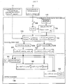
- Fig. 5 is a block diagram illustrating an automatic synchronous parallelization apparatus 17 according to the embodiment of the present invention.
- Fig. 5 shows: a single-phase voltage-type DC-to-AC converting device 11 that performs an autonomous parallel operation; an external single-phase AC voltage source 12 that is in parallel therewith; a coordination switch 15 that performs parallel connection or disconnection of the single-phase voltage-type DC-to-AC converting device 11 and the external single-phase AC voltage source 12.
- the external single-phase AC voltage source 12 for example, is a power system or a power generator.
- the single-phase voltage-type DC-to-AC converting device 11 is a single-phase voltage-type DC-to-AC converting device that performs an autonomous parallel operation described in JP-A No. 09-028040 .
- the output terminal voltage V 1 (t) of the single-phase voltage-type DC-to-AC converting device 11 that performs an independent unloaded operation is represented by the following equation.
- V 1 t 2 ⁇ V i ⁇ sin ⁇ t V
- V i is the effective value of the voltage
- ⁇ i is the test source angular frequency of the single-phase voltage-type DC-to-AC converting device 11.
- E co is a reference voltage
- K mu1 is the 1st-axis voltage gain
- K mu2 is the 2nd-axis voltage gain
- K f is a phase locked loop (PLL) gain.
- ⁇ i leads as the 2nd-axis voltage command value V 2 * of the inverter increases, and lags as the 2nd-axis voltage command value V 2 * of the inverter decreases.
- V i increases as the 1st-axis voltage command value V 1 * is increased, and decreases as the 1st-axis voltage command value V 1 * is decreased.
- the amplitude, the frequency, and the phase can be independently changed in accordance with V 1 * and V 2 *.
- the automatic synchronous parallelization apparatus 17 includes a synchronization detecting circuit 130, a voltage amplitude command value generating circuit 180, and a frequency command value generating circuit 190.
- the synchronization detecting circuit 130 detects a value [( ⁇ s )- ⁇ )V s or ( ⁇ s - ⁇ ) V s 2 ] relating to a frequency difference between the external single-phase AC voltage source 12 that is in parallel with the single-phase voltage-type DC-to-AC converting device 11 that performs an autonomous parallel operation based on the 1st-axis voltage command value V 1 * used for adjusting the amplitude of the output single-phase AC voltage waveform and the 2nd-axis voltage command value V 2 * used for adjusting the frequency and the single-phase voltage-type DC-to-AC converting device 11 and a value [V s or V s 2 ] relating to the effective value of the voltage of the external single-phase AC voltage source 12.
- the voltage amplitude command value generating circuit 180 generates the 1st-axis voltage command value V 1 * at which the effective value V i of the single-phase AC voltage of the single-phase voltage-type DC-to-AC converting device 11 approaches the effective value V s of the voltage of the external single-phase AC voltage source 12 that is detected by the synchronization detecting circuit 130 and inputs the 1st-axis voltage command value V 1 * to the single-phase voltage-type DC-to-AC converting device 11.
- the frequency command value generating circuit 190 generates the 2nd-axis voltage command value V 2 * for which the frequency of the single-phase AC voltage of the single-phase voltage-type DC-to-AC converting device 11 is a frequency that is shifted from the frequency of the external single-phase AC voltage source 12 by an arbitrary frequency value ⁇ 0 by using the value relating to the frequency difference detected by the synchronization detecting circuit 130 and inputs the 2nd-axis voltage command value V 2 * to the single-phase voltage-type DC-to-AC converting device 11.
- the synchronization detecting circuit 130 that can detect the value [( ⁇ s - ⁇ )V s or ( ⁇ s -( ⁇ ) V s 2 ] relating to a frequency difference between the external single-phase AC voltage source 12 and the single-phase voltage-type DC-to-AC converting device 11 and the value [V s or V s 2 ] relating to the effective value of the voltage of the external single-phase AC voltage source 12 may be used.
- Fig. 1 is a schematic diagram illustrating the synchronization test performed between the target single-phase AC voltage source 11 and a target single-phase AC voltage source 12.
- the AC-to-DC converter single-phase AC voltage source 11 for example, is a single-phase AC power source in which a synchronization detecting circuit is built such as an inverter that performs an autonomous parallel operation (APRun).
- the target single-phase AC voltage source 12, for example, is a power system or an external AC power source that is the other party for parallelization.
- the output terminal voltage V fil (t) is represented by the following equation.
- V fil t 2 ⁇ V i ⁇ sin ⁇ t V
- V i is an effective value of the voltage of the AC-to-DC converter single-phase AC voltage source 11.
- V sys (t) of the target single-phase AC voltage source 12 is represented by the following equation.
- V sys t 2 ⁇ V s ⁇ sin ⁇ s ⁇ t + ⁇ V
- V s is an effective value [V]
- ⁇ s is an angular frequency [rad/s]
- V # sys (t) that lags by ⁇ / (2 ⁇ co ) [s] with respect to V sys (t)
- ⁇ co is the reference angular frequency [rad/s] of the synchronization detecting circuit. Since ⁇ co cannot be determined to coincide with ⁇ s , V # sys (t) cannot be determined to precisely lag by ⁇ /2 with respect to V sys (t).
- V sys # t ⁇ V sys ⁇ t - ⁇ 2 ⁇ ⁇ co V V # sys (t) is transformed as follows.
- ⁇ i the phase angle of the AC-to-DC converter single-phase AC voltage source.
- V 3 t V 4 t 1 2 ⁇ sin ⁇ i - cos ⁇ i cos ⁇ i sin ⁇ i ⁇ V sys t V sys # t
- V 3 (t) and V 4 (t) acquired through Mathematical Expression A9 are respectively called a frequency difference cosine signal and a frequency difference sine signal.
- This part influences the amplitude . This part corresponds to the difference of the phase .
- V u3 (t) is approximately the same as the following value.
- This part influences the amplitude . This part corresponds to the difference of the phase .
- V u4 (t) is approximately the same as the following value.
- V U ⁇ 3 2 t + V U ⁇ 4 2 t V s 2 ⁇ cos 2 ⁇ ⁇ ⁇ ⁇ co - ⁇ s 4 ⁇ ⁇ co
- V U ⁇ 3 t ⁇ d ⁇ V U ⁇ 4 dt t + V U ⁇ 4 t ⁇ d ⁇ V U ⁇ 3 dt t V U ⁇ 3 2 t + V U ⁇ 4 2 t ⁇ s - ⁇
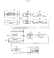
- Fig. 2 is a schematic diagram illustrating the synchronization detecting circuit 130 of this embodiment.
- the synchronization detecting circuit 130 includes: a reference angular frequency ⁇ co ; a sampler 133 that detects the target voltage waveform of the target-target single-phase AC voltage source 12; a delay circuit 134 that generates a delayed voltage waveform, which is acquired by delaying the target voltage waveform by time (m-1/2) ⁇ / ⁇ co (here, m is a natural number), detected by the sampler 133; and a calculation unit 135 that calculates a frequency difference cosine signal and a frequency difference sine signal that have an angular frequency of a difference between the target angular frequency ⁇ s of the target voltage waveform and the DC-to-AC converter angular frequency ⁇ , based on the target voltage waveform detected by the sampler 133, the delayed voltage waveform generated by the delay circuit 134, and the given the angular frequency ⁇ of the AC-to-DC converter
- the synchronization detecting circuit 130 includes the reference angular frequency ⁇ co .
- the reference angular frequency may be configured to be received from the AC-to-DC converter single-phase AC voltage source 11.
- the test-source voltage waveform V 1 (t) of the single-phase AC voltage source 11 can be represented in the following equation.
- V 1 t V ⁇ sin ⁇ co ⁇ t V
- the target voltage waveform V 2 (t) of the single-phase AC voltage source 12 that becomes a test target can be represented in the following equation.
- V 2 t V s ⁇ sin ⁇ s ⁇ t + ⁇ V
- the sampler 133 samples the target voltage waveform V 2 (t).
- a sample waveform acquired by sampling the target voltage waveform V 2 (t) is represented as V 2 (nTs).
- Ts is a sampling period
- n is a sampling number.
- the delay circuit 134 receives the reference angular frequency ⁇ co as input and generates a delayed voltage waveform V 2 # (nTs) acquired by delaying the sample waveform V 2 (nTs) by a period of (m-1/2) ⁇ / ⁇ co (here, m is a natural number).
- the delay amount of the delayed voltage waveform V 2 # (nTs) can be represented as (m-1/2) ⁇ / ⁇ co .
- m 1 (a case of 1/4 period delay) will be described.
- the delayed voltage waveform V 2 # (nTs) becomes the following equation.
- V 2 # nTs V 2 ⁇ n ⁇ s ⁇ Ts - ⁇ 2 ⁇ ⁇ co V
- the calculation unit 135 receives the DC-to-AC converter angular frequency ⁇ as input from the single-phase AC voltage source 11.
- the calculation unit 135 receives the sample waveform V 2 (nTs) and the delayed voltage waveform V 2 # (nTs) as input and calculates a frequency difference cosine signal V 3 (nTs) and a frequency difference sine signal V 4 (nTs) that have an angular frequency of a difference between the DC-to-AC converter angular frequency ⁇ and the target angular frequency ⁇ s of the single-phase AC voltage source 12.
- the calculation unit 135 calculates the frequency difference cosine signal V 3 (nTs) and the frequency difference sine signal V 4 (nTs) by performing rotating coordinate conversion for the sample waveform V 2 (nTs) and the delayed voltage waveform V 2 # (nTs), as represented in Mathematical Expression A1.
- the frequency difference cosine signal V 3 (nTs) and the frequency difference sine signal V 4 (nTs) include high frequency components of a frequency ( ⁇ s + ⁇ ).
- the calculation unit 135 further includes low pass filters (152A and 152B) that eliminate the high-frequency components.
- the frequency difference cosine signal and the frequency difference sine signal from which the high-frequency components are eliminated by using the low-pass filters (152A and 152B) are respectively denoted as V u3 (nTs) and V u4 (nTs).
- the synchronization detecting circuit 130 further includes a detection unit 136.
- the detection unit 136 can detect an effective value of the voltage of the target voltage waveform V 2 (t), a frequency difference between the target angular frequency ⁇ s of the target voltage waveform V 2 (t) and the DC-to-AC converter angular frequency ⁇ , and a phase difference between the target voltage waveform V 2 (t) and the test-source voltage waveform V 1 (t) by using the frequency difference cosine signal V u3 (nTs) and the frequency difference sine signal V u4 (nTs) output by the calculation unit 135.
- the detection unit 136 detects the effective value of the voltage, the frequency difference, and the phase difference by using a circuit 161 that calculates Mathematical Expression A2, a circuit 162 that calculates Mathematical Expression A3, and a circuit 163 that calculates Mathematical Expression A4.
- the synchronization detecting circuit 130 may input information of the effective value of the voltage, the frequency difference, and the phase difference, which have been detected, to the single-phase AC voltage source 11.
- the single-phase AC voltage source 11 can adjust the voltage amplitude value V, the DC-to-AC converter angular frequency ⁇ , and the phase of the test-source voltage waveform V1 (t) so as to coincide with the voltage amplitude value V s , the target angular frequency ⁇ s , and the phase ⁇ of the single-phase AC voltage source 12, based on the above-described information.
- the single-phase AC voltage source 11 can be connected to the single-phase AC voltage source 12 by being synchronized to the signal-phase AC voltage source 12.
- the synchronization detecting circuit 130 has been described to be arranged outside the single-phase AC voltage source 11.
- the single-phase AC voltage source 11 may have the synchronization detecting circuit 130 built therein.
- the delay time of the delay circuit 134 has been described as (m-1/2) ⁇ / ⁇ co .
- the delay circuit 134 generates the delayed voltage waveform V 2 * (nTs) by delaying the sample waveform V 2 (nTs) by a period other than a (2m-1) /2 period and the m period.
- the delayed voltage waveform V 2 # (nTs) may have a delay of a 1/6 period, a 2/6 period, a 4/6 period, a 5/6 period, ⁇ , or a p/6 period (here, p is a natural number that is not a multiple number of three).
- the delayed voltage waveform V 2 # (nTs) may have a delay of a 1/4 period, a 3/4 period, ⁇ , or a q/4 period (here, q is an odd number).
- the coefficient of the matrix represented in Mathematical Expression A1 has been described as 1/ ⁇ 2.
- the coefficient may be an arbitrary number other than zero.
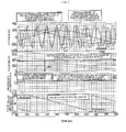
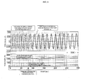
- Fig. 3 is a result of simulating a detection of the voltage amplitude V s of the single-phase AC voltage source 12, a frequency difference between the single-phase AC voltage source 11 and the single-phase AC voltage source 12, and a phase difference therebetween that is performed by the synchronization detecting circuit 130.
- the frequency difference cosine signals V u3 (nTs) and V u4 (nTs) that are generated based on the target voltage waveform V 2 (t) of the single-phase AC voltage source 12 and a delayed voltage waveform V 2 # (t) acquired by delaying the target voltage waveform by a 0.25 cycle have an amplitude of 180 V (the effective value of the voltage of the single-phase AC voltage source 12) and a frequency of 4 Hz (a frequency of a difference between the frequency of the test-source voltage waveform and the frequency of the target voltage waveform).
- the detection unit 136 detects the effective value of the voltage as 180 V, which is the same as that of the single-phase AC voltage source 12. In addition, the detection unit 136 detects a frequency difference as "-4 Hz,” which is same as the set frequency difference (a frequency difference of the single-phase AC voltage source 12 with respect to the single-phase AC voltage source 11) between the single-phase AC voltage source 11 and the single-phase AC voltage source 12. Furthermore, the detection unit 136 detects a phase difference that is generated based on the frequency difference.
- the synchronization detecting circuit 130 can precisely detect the effective value of the voltage of the single-phase AC voltage source 12, the frequency difference between the single-phase AC voltage source 11 and the single-phase AC voltage source 12, and the phase difference between the single-phase AC voltage source 11 and the single-phase AC voltage source 12.
- Fig. 2 is a schematic diagram illustrating the synchronization detecting circuit 130.
- the synchronization detecting circuit 130 includes: a reference angular frequency ⁇ co ; a sampler 133 that detects the target voltage waveform of the external single-phase AC voltage source 12; a delay circuit 134 that generates a delayed voltage waveform, which is acquired by delaying the target voltage waveform by time (m-1/2) ⁇ / ⁇ co (here, m is a natural number), detected by the sampler 133; and a calculation unit 135 that calculates a frequency difference cosine signal and a frequency difference sine signal that have an angular frequency of a difference between the target angular frequency ⁇ s of the target external voltage waveform and the DC-to-AC converter angular frequency ⁇ , based on the target external voltage waveform detected by the sampler 133, the delayed voltage waveform generated by the delay circuit 134, and the given the angular frequency ⁇ of the single-phase voltage-type DC-to-AC converting device 11.
- the synchronization detecting circuit 130 includes the reference angular frequency ⁇ co .
- the reference angular frequency may be configured to be received from the test-source single-phase voltage-type DC-to-AC converting device 11.
- the target voltage waveform V 2 (t) of the external single-phase AC voltage source 12 that becomes a test target can be represented in the following equation.
- V 2 t V s ⁇ sin ⁇ s ⁇ t + ⁇ V
- V s is an effective value [V]
- ⁇ s is an angular frequency [rad/s]
- the sampler 133 samples the target external voltage waveform V 2 (t).
- a sample waveform acquired by sampling the target voltage waveform V 2 (t) is represented as V 2 (nTs).
- Ts is a sampling period
- n is a sampling number.
- the delay circuit 134 receives the reference angular frequency ⁇ co as input and generates a delayed voltage waveform V 2 # (nTs) acquired by delaying the sample waveform V 2 (nTs) by a period of (m-1/2) ⁇ / ⁇ co (here, m is a natural number).
- the delay amount of the delayed voltage waveform V 2 # (nTs) can be represented as (m-1/2) ⁇ / ⁇ co .
- m 1 (a case of 1/4 period delay) will be described.
- the delayed voltage waveform V 2 # (nTs) becomes the following equation.
- V 2 # nTs V 2 ⁇ n ⁇ s ⁇ Ts - ⁇ 2 ⁇ ⁇ co V
- the calculation unit 135 receives the DC-to-AC converter angular frequency ⁇ as input from the single-phase voltage-type DC-to-AC converting device 11.
- the calculation unit 135 receives the sample waveform V 2 (nTs) and the delayed voltage waveform V 2 # (nTs) as input and calculates a frequency difference cosine signal V 3 (nTs) and a frequency difference sine signal V 4 (nTs) that have an angular frequency of a difference between the DC-to-AC converter angular frequency ⁇ and the target angular frequency ⁇ s of the external single-phase AC voltage source 12.
- the rotational coordinate conversion circuit 151 in the calculation unit 135 calculates the frequency difference cosine signal V 3 (nTs) and the frequency difference sine signal V 4 (nTs) by performing rotating coordinate conversion for the sample waveform V 2 (nTs) and the delayed voltage waveform V 2 # (nTs), as represented in Mathematical Expression B5.
- V 3 nTs V 4 nTs 1 2 ⁇ sin n ⁇ Ts - 1 m ⁇ cos n ⁇ Ts cos n ⁇ Ts - - 1 m ⁇ sin n ⁇ Ts ⁇ V 2 nTs V 2 # nTs
- the frequency difference cosine signal V 3 (nTs) and the frequency difference sine signal V 4 (nTs) include high frequency components of a frequency ( ⁇ s + ⁇ ).
- the calculation unit 135 further includes low pass filters (152A and 152B) that eliminate the high-frequency components.
- the frequency difference cosine signal and the frequency difference sine signal from which the high-frequency components are eliminated by using the low-pass filters (152A and 152B) are respectively denoted as V u3 (nTs) and V u4 (nTs).
- Frequency difference cosine signal output terminal 153 and frequency difference sine signal output terminal 154 output V u3 (nTs) and V u4 (nTs) respectively.
- the synchronization detecting circuit 130 further includes a detection unit 136.
- the detection unit 136 can detect an effective value of the voltage of the target external voltage waveform V 2 (t), a frequency difference between the target angular frequency ⁇ s of the target external voltage waveform V 2 (t) and the DC-to-AC converter angular frequency ⁇ , and a phase difference between the target external voltage waveform V 2 (t) and the test-source voltage waveform V 1 (t) by using the frequency difference cosine signal V u3 (nTs) and the frequency difference sine signal V u4 (nTs) output by the calculation unit 135.
- the detection unit 136 detects the effective value of the voltage, the frequency difference, and the phase difference by using a circuit 161 that calculates Mathematical Expression B7, a circuit 162 that calculates Mathematical Expression B8, and a circuit 163 that calculates Mathematical Expression B9.
- Vs V U ⁇ 3 2 nTs + V U ⁇ 4 2 nTs
- the voltage amplitude command value generating circuit 180 includes: a voltage system subtractor 181 that subtracts a value [V i or V i 2 ] relating to the effective value of the voltage of the single-phase AC voltage that is output by the single-phase voltage-type DC-to-AC converting device 11 from the a value [V s or V s 2 ] relating to the effective value of the voltage of the external single-phase AC voltage source 12 that is detected by the synchronization detecting circuit 130; a voltage system integrator 182 that integrates a value acquired through subtraction of the voltage system subtractor 181; and a voltage system adder 183 that generates the 1st-axis voltage command value V 1 * (t) by adding the initial voltage value V 1 * (0) of the single-phase AC voltage waveform of the single-phase voltage-type DC-to-AC converting device 11 immediately prior to the start of automatic parallel control with the external single-phase AC voltage source 12 and the value integrated by the voltage system integrator 182.
- V u3 2 (t) + V u4 2 (t) is almost the same as V s 2 .
- V 1 * t V 1 * 0 + K amp ⁇ 0 t V U ⁇ 3 2 t + V U ⁇ 4 2 t - V i 2 t ⁇ dt
- V 1 * (0) is a value of the V 1 * (t) immediately prior to the start of the closed looping control
- K amp (> 0) is an integral gain.
- Mathematical Expression B11 can be approximated as follows.
- K mu ⁇ 1 V 1 * 0 + K amp ⁇ 0 t V s 2 - V i 2 t ⁇ dt
- V i t V i 0 + K mu ⁇ 1 ⁇ K amp 1 + K mu ⁇ 1 ⁇ 0 t V s 2 - V i 2 t ⁇ dt
- V i (0) (E co +K mu1 ⁇ V 1 * (0)) / (1+K mu1 )
- V 1 (0) i the effective value of the voltage of the single-phase voltage-type DC-to-AC converting device 11 immediately prior to the start of automatic parallel control.
- V i t C - exp - 2 ⁇ K mu ⁇ 1 ⁇ K amp 1 + K mu ⁇ 1 ⁇ V s ⁇ t C + exp - 2 ⁇ K mu ⁇ 1 ⁇ K amp 1 + K mu ⁇ 1 ⁇ V s ⁇ t ⁇ V s
- V i t V s + V i 0 - V s - V i 0 ⁇ exp - 2 ⁇ K mu ⁇ 1 ⁇ K amp 1 + K mu ⁇ 1 ⁇ V s ⁇ t V s + V i 0 + V s - V i 0 ⁇ exp - 2 ⁇ K mu ⁇ 1 ⁇ K amp 1 + K mu ⁇ 1 ⁇ V s ⁇ t ⁇ V s From Mathematical Expression B19, Mathematical Expression B20 can be acquired.
- the frequency command value generating circuit 190 includes: a frequency system calculator 191 that adds a value [( ⁇ - ⁇ ) ⁇ V s or ( ⁇ s -( ⁇ ) ⁇ V s 2 ] relating to a frequency difference detected by the synchronization detecting circuit 130 to a value acquired by multiplying a value [V s or V s 2 ] relating to the effective value of the voltage of the external single-phase AC voltage source 12 detected by the synchronization detecting circuit 130 by an arbitrary frequency value ⁇ o ; a frequency system integrator 192 that integrates the value calculated by the frequency system calculator 191; and a frequency system adder 193 that generates the 2nd-axis voltage command value V 2 * (t) by adding the initial frequency value V 2 * (0) of the single-phase AC voltage waveform of the single-phase voltage-type DC-to-AC converting device 11 immediately prior to the start of automatic parallel control with the external single-phase AC voltage source 12 and the value integrated by the frequency system integrator 192.
- V 2 * (0) is a value of the V 2 * (t) immediately prior to the start of the closed looping control
- K freq (> 0) is an integral gain.
- the value of V s 2 that is multiplied by ⁇ 0 is acquired by using Mathematical Expression B10. V s 2 may be substituted with E co 2 .
- ⁇ i (0) is the value of ⁇ i (t) immediately before the start of closed looping.
- the angular frequency of the output of the single-phase voltage-type DC-to-AC converting device 11 becomes close to ⁇ s + ⁇ o in accordance with the closed looping control as time elapses.
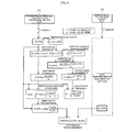
- Fig. 6 is a diagram illustrating the logic for having the single-phase voltage-type DC-to-AC converting device 11 to be parallelized with the external single-phase AC voltage source 12, which is performed by the automatic synchronous parallelization apparatus 17. It is assumed that a parallelization command is issued (Step S01) when the coordination switch 15 is in an open state (Step S02). The automatic synchronous parallelization apparatus 17 starts V 1 * closed looping and V 2 * closed looping (Steps S03 and S04). The automatic synchronous parallelization apparatus 17 checks the following four conditions. The first condition is
- ⁇ V s represents an allowable amplitude difference and is, for example, about 5% of V s .
- the second condition is
- ⁇ represents an allowable difference of the angular frequency and is, for example, about 1% of ⁇ s .
- the third condition is that V u3 (t) calculated by the synchronization detecting circuit 130 is greater than zero (Step S07).
- the fourth condition is
- ⁇ i represents an allowable phase difference and is, for example, about 5 degrees.
- Step S07 is equal to the condition of cos ( ⁇ s t - ⁇ i (t)) > 0. This is a condition for excluding a case where parallelization is made with a phase difference of 180° under the condition used in Step S08.
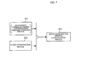
- Fig. 7 is a diagram illustrating the logic for disconnecting the single-phase voltage-type DC-to-AC converting device 11 from the external single-phase AC voltage source 12, which is performed by the automatic synchronous parallelization apparatus 17. It is assumed that a disconnection command is issued (Step S21) when the coordination switch 15 is in a closed state (Step S22). The automatic synchronous parallelization apparatus 17 issues a command for opening the coordination switch 15 (Step S23). When receiving the command, the coordination switch 15 is open.
- Fig. 8 is a result of simulating the 1st-axis voltage command value, the 2nd-axis voltage command value, and the single-phase voltage waveform of the single-phase voltage-type DC-to-AC converting device 11 when the automatic synchronous parallelization apparatus 17 connects the single-phase voltage-type DC-to-AC converting device 11 so as to be in parallel with the external single-phase AC voltage source 12.
- the single-phase voltage-type DC-to-AC converting device 11 is operated at 200 V and 50 Hz before a parallelization process.
- the external single-phase AC voltage source 12 is operated at 220 V and 54 Hz.
- the coordination command (Step S01) represented in Fig. 6 was performed. Thereafter, the voltage waveform command value slowly increases from 200 V and becomes constant at 240 V (corresponding to an output voltage of 220 V).
- the amplitude value of the signal-phase AC voltage of the single-phase voltage-type DC-to-AC converting device 11 becomes close to the amplitude value of the AC voltage waveform of the external single-phase AC voltage source 12.
- the 2nd-axis voltage command value also slowly increases from 0 V and becomes constant at 41.3 V. This voltage corresponds to the frequency of 54.05 Hz of the single-phase AC voltage waveform of the single-phase voltage-type DC-to-AC converting device 11.
- the magnitude and the frequency of the output voltage of the single-phase voltage-type DC-to-AC converting device 11 slowly becomes close to the voltage and the frequency of the external single-phase AC voltage source 12, and coincides therewith after about 150 ms . In other words, it takes about 150 ms for the single-phase AC voltage waveform of the single-phase voltage-type DC-to-AC converting device 11 to be synchronized with the voltage waveform of the external single-phase AC voltage source 12.
- Figs. 9A and 9B are results of measurements of the single-phase voltage waveform of the single-phase voltage-type DC-to-AC converting device 11, the voltage waveform of the external single-phase AC voltage source 12, and the output current of the single-phase voltage-type DC-to-AC converting device 11 before and after the parallelization process in this experiment.
- Fig. 9A is a waveform before the parallelization process
- Fig. 9B is a waveform immediately before and after the parallelization process.
- the single-phase voltage waveform of the single-phase voltage-type DC-to-AC converting device 11 and the voltage waveform of the external single-phase AC voltage source 12 are mismatched to each other.
- the parallelization process is performed in accordance with the parallelization command with the single-phase voltage waveform of the single-phase voltage-type DC-to-AC converting device 11 and the voltage waveform of the external single-phase AC voltage source 12 being synchronized with each other, before the parallel connection, the single-phase voltage waveform of the single-phase voltage-type DC-to-AC converting device 11 and the voltage waveform of the external single-phase AC voltage source 12 coincide with each other.
- the automatic synchronous parallelization apparatus 17 can have a single-phase voltage-type DC-to-AC converting device, which is controlled as a voltage source, to be parallelized with an external single-phase AC voltage source.
Applications Claiming Priority (2)
| Application Number | Priority Date | Filing Date | Title |
|---|---|---|---|
| JP2010013527A JP5394945B2 (ja) | 2010-01-25 | 2010-01-25 | 同期検定装置 |
| JP2010050751A JP5600016B2 (ja) | 2010-03-08 | 2010-03-08 | 自動同期並列装置 |
Publications (3)
| Publication Number | Publication Date |
|---|---|
| EP2348628A2 true EP2348628A2 (fr) | 2011-07-27 |
| EP2348628A3 EP2348628A3 (fr) | 2012-05-30 |
| EP2348628B1 EP2348628B1 (fr) | 2014-12-03 |
Family
ID=44144865
Family Applications (1)
| Application Number | Title | Priority Date | Filing Date |
|---|---|---|---|
| EP11152107.6A Not-in-force EP2348628B1 (fr) | 2010-01-25 | 2011-01-25 | Circuit de détection de synchronisation et appareil de parallélisation synchrone automatique |
Country Status (4)
| Country | Link |
|---|---|
| US (1) | US8553436B2 (fr) |
| EP (1) | EP2348628B1 (fr) |
| CN (1) | CN102193023B (fr) |
| HK (1) | HK1161354A1 (fr) |
Cited By (3)
| Publication number | Priority date | Publication date | Assignee | Title |
|---|---|---|---|---|
| WO2016206688A1 (fr) * | 2015-06-24 | 2016-12-29 | Vestas Wind Systems A/S | Courant d'appel commandé destiné à un filtre réseau connecté à un convertisseur |
| EP3188338A1 (fr) * | 2015-12-30 | 2017-07-05 | Sungrow Power Supply Co., Ltd. | Procédé de commande raccordé au réseau sur la base d'un synchroniseur virtuel et dispositif associé |
| CN113359021A (zh) * | 2021-06-23 | 2021-09-07 | 深圳市锦祥自动化设备有限公司 | 静态同期检查继电器及高精度相位差和幅值差判断系统 |
Families Citing this family (6)
| Publication number | Priority date | Publication date | Assignee | Title |
|---|---|---|---|---|
| IN2013CH04376A (fr) * | 2013-09-26 | 2015-04-03 | Abb Technology Ltd | |
| CN104808061B (zh) * | 2014-01-26 | 2017-12-12 | 南京邮电大学 | 一种电信号相位差的测量方法 |
| CN104808059B (zh) * | 2014-01-26 | 2017-12-08 | 南京邮电大学 | 一种电信号瞬时相位的数字化测量方法 |
| CN104266732B (zh) * | 2014-10-24 | 2017-06-30 | 广州能源检测研究院 | 双台位流量计检定装置脉冲计数精度补偿方法 |
| CN110138001A (zh) * | 2018-02-09 | 2019-08-16 | 无锡美凯能源科技有限公司 | 一种应用于微电网逆变装置的相序识别及自调整方法 |
| US11245266B2 (en) * | 2018-11-13 | 2022-02-08 | Kohler Co. | Offline synchronization of generators |
Citations (4)
| Publication number | Priority date | Publication date | Assignee | Title |
|---|---|---|---|---|
| JPS5240174A (en) | 1975-09-25 | 1977-03-28 | Tokyo Electric Power Co Inc:The | Digital type synchronous detection system |
| JPH05240174A (ja) | 1992-03-03 | 1993-09-17 | Mitsubishi Heavy Ind Ltd | スクロール型流体機械 |
| JPH0928040A (ja) | 1995-07-13 | 1997-01-28 | Toshiba Corp | 系統連系インバータ装置の起動運転方法 |
| JP2009219263A (ja) | 2008-03-11 | 2009-09-24 | Origin Electric Co Ltd | 単相電圧型交直変換装置 |
Family Cites Families (7)
| Publication number | Priority date | Publication date | Assignee | Title |
|---|---|---|---|---|
| TW245848B (fr) | 1991-09-18 | 1995-04-21 | Toshiba Kk | |
| JPH06292365A (ja) * | 1992-10-30 | 1994-10-18 | Fuji Electric Co Ltd | Pwmインバータの制御方法および制御装置 |
| JPH06189476A (ja) | 1992-12-18 | 1994-07-08 | Yuasa Corp | 無停電電源装置の制御装置 |
| CN1303739C (zh) | 2003-05-20 | 2007-03-07 | 西安交通大学 | 正弦脉宽调制逆变电源的自动主从并联控制方法 |
| US7183667B2 (en) | 2003-12-19 | 2007-02-27 | Square D Company | Method and apparatus for power inverter synchronization |
| CN101534065B (zh) | 2009-04-20 | 2010-12-01 | 浙江大学 | 一种并网三相电压源变换器的不对称直接功率控制方法 |
| JP5240174B2 (ja) | 2009-11-27 | 2013-07-17 | トヨタ自動車株式会社 | 電動機の冷却構造 |
-
2011
- 2011-01-14 US US13/006,636 patent/US8553436B2/en not_active Expired - Fee Related
- 2011-01-25 CN CN201110026452.3A patent/CN102193023B/zh not_active Expired - Fee Related
- 2011-01-25 EP EP11152107.6A patent/EP2348628B1/fr not_active Not-in-force
- 2011-12-22 HK HK11113838.6A patent/HK1161354A1/xx not_active IP Right Cessation
Patent Citations (4)
| Publication number | Priority date | Publication date | Assignee | Title |
|---|---|---|---|---|
| JPS5240174A (en) | 1975-09-25 | 1977-03-28 | Tokyo Electric Power Co Inc:The | Digital type synchronous detection system |
| JPH05240174A (ja) | 1992-03-03 | 1993-09-17 | Mitsubishi Heavy Ind Ltd | スクロール型流体機械 |
| JPH0928040A (ja) | 1995-07-13 | 1997-01-28 | Toshiba Corp | 系統連系インバータ装置の起動運転方法 |
| JP2009219263A (ja) | 2008-03-11 | 2009-09-24 | Origin Electric Co Ltd | 単相電圧型交直変換装置 |
Cited By (5)
| Publication number | Priority date | Publication date | Assignee | Title |
|---|---|---|---|---|
| WO2016206688A1 (fr) * | 2015-06-24 | 2016-12-29 | Vestas Wind Systems A/S | Courant d'appel commandé destiné à un filtre réseau connecté à un convertisseur |
| US10590914B2 (en) | 2015-06-24 | 2020-03-17 | Vestas Wind Systems A/S | Controlled inrush current for converter-connected grid filter |
| EP3188338A1 (fr) * | 2015-12-30 | 2017-07-05 | Sungrow Power Supply Co., Ltd. | Procédé de commande raccordé au réseau sur la base d'un synchroniseur virtuel et dispositif associé |
| CN113359021A (zh) * | 2021-06-23 | 2021-09-07 | 深圳市锦祥自动化设备有限公司 | 静态同期检查继电器及高精度相位差和幅值差判断系统 |
| CN113359021B (zh) * | 2021-06-23 | 2022-10-21 | 深圳市锦祥自动化设备有限公司 | 静态同期检查继电器及高精度相位差和幅值差判断系统 |
Also Published As
| Publication number | Publication date |
|---|---|
| EP2348628A3 (fr) | 2012-05-30 |
| US8553436B2 (en) | 2013-10-08 |
| US20110182091A1 (en) | 2011-07-28 |
| CN102193023B (zh) | 2015-02-18 |
| EP2348628B1 (fr) | 2014-12-03 |
| HK1161354A1 (en) | 2012-08-24 |
| CN102193023A (zh) | 2011-09-21 |
Similar Documents
| Publication | Publication Date | Title |
|---|---|---|
| EP2348628B1 (fr) | Circuit de détection de synchronisation et appareil de parallélisation synchrone automatique | |
| Rodriguez et al. | Multiple second order generalized integrators for harmonic synchronization of power converters | |
| CN109067393B (zh) | 一种电力系统的锁相方法、装置及设备 | |
| Karimi-Ghartemani et al. | A new phase-locked loop system for three-phase applications | |
| EP2472709A2 (fr) | Redresseur commandé monophasée | |
| US10256747B2 (en) | Electric power conversion device and electric power conversion system | |
| CN110557118B (zh) | 一种锁相装置及锁相方法 | |
| US20110128054A1 (en) | Phase lock loop with tracking filter for synchronizing an electric grid | |
| EP0239806A1 (fr) | Dispositif de stabilisation des oscillations de torsion d'un arbre turbine-générateur | |
| KR101380380B1 (ko) | 전력계통의 상태에 따른 적응형 위상추종 방법 및 시스템 | |
| KR20150036966A (ko) | Hvdc 시스템의 컨버터 제어 장치 | |
| JPH07200084A (ja) | 電力変換装置 | |
| JP3561119B2 (ja) | 同期制御方法、周波数検出方法及び同期制御装置 | |
| JP5600016B2 (ja) | 自動同期並列装置 | |
| Winter et al. | Analysis of an sDFT-PLL for Grid-Forming Control Methods | |
| KR101545139B1 (ko) | Lpn 필터를 이용한 전력계통의 위상추종 시스템 | |
| US11043803B2 (en) | Reference signal generating method for distance and directional protection elements | |
| JP6263990B2 (ja) | 交直変換装置の同期制御回路 | |
| WO2014050759A1 (fr) | Convertisseur alternatif-continu de type tension à phase unique | |
| JP3958255B2 (ja) | 発電機における位相同期検出回路 | |
| US11329503B2 (en) | Synchronization control circuit and uninterruptible power supply apparatus including the same | |
| Mirbod et al. | Performance analysis of a novel microprocessor-based controller for a phase-controlled rectifier connected to a weak AC system | |
| WO2014050758A1 (fr) | Dispositif de conversion alternatif-continu de type tension à phase unique | |
| Hou et al. | Analysis of prefilter phase-locked loop under interharmonics perturbation | |
| Chen et al. | Positive sequence detector based on cascaded delayed quadrature signal cancellation |
Legal Events
| Date | Code | Title | Description |
|---|---|---|---|
| PUAI | Public reference made under article 153(3) epc to a published international application that has entered the european phase |
Free format text: ORIGINAL CODE: 0009012 |
|
| AK | Designated contracting states |
Kind code of ref document: A2 Designated state(s): AL AT BE BG CH CY CZ DE DK EE ES FI FR GB GR HR HU IE IS IT LI LT LU LV MC MK MT NL NO PL PT RO RS SE SI SK SM TR |
|
| AX | Request for extension of the european patent |
Extension state: BA ME |
|
| PUAL | Search report despatched |
Free format text: ORIGINAL CODE: 0009013 |
|
| AK | Designated contracting states |
Kind code of ref document: A3 Designated state(s): AL AT BE BG CH CY CZ DE DK EE ES FI FR GB GR HR HU IE IS IT LI LT LU LV MC MK MT NL NO PL PT RO RS SE SI SK SM TR |
|
| AX | Request for extension of the european patent |
Extension state: BA ME |
|
| RIC1 | Information provided on ipc code assigned before grant |
Ipc: H02M 7/5387 20070101ALI20120420BHEP Ipc: H02M 7/493 20070101AFI20120420BHEP |
|
| 17P | Request for examination filed |
Effective date: 20121130 |
|
| RIC1 | Information provided on ipc code assigned before grant |
Ipc: H02M 7/493 20070101AFI20140430BHEP Ipc: H02J 3/42 20060101ALI20140430BHEP Ipc: H02M 7/5387 20070101ALI20140430BHEP |
|
| GRAP | Despatch of communication of intention to grant a patent |
Free format text: ORIGINAL CODE: EPIDOSNIGR1 |
|
| INTG | Intention to grant announced |
Effective date: 20140626 |
|
| GRAS | Grant fee paid |
Free format text: ORIGINAL CODE: EPIDOSNIGR3 |
|
| GRAA | (expected) grant |
Free format text: ORIGINAL CODE: 0009210 |
|
| AK | Designated contracting states |
Kind code of ref document: B1 Designated state(s): AL AT BE BG CH CY CZ DE DK EE ES FI FR GB GR HR HU IE IS IT LI LT LU LV MC MK MT NL NO PL PT RO RS SE SI SK SM TR |
|
| REG | Reference to a national code |
Ref country code: GB Ref legal event code: FG4D |
|
| REG | Reference to a national code |
Ref country code: CH Ref legal event code: EP Ref country code: AT Ref legal event code: REF Ref document number: 699870 Country of ref document: AT Kind code of ref document: T Effective date: 20141215 |
|
| REG | Reference to a national code |
Ref country code: IE Ref legal event code: FG4D |
|
| REG | Reference to a national code |
Ref country code: DE Ref legal event code: R096 Ref document number: 602011011828 Country of ref document: DE Effective date: 20150115 |
|
| REG | Reference to a national code |
Ref country code: NL Ref legal event code: VDEP Effective date: 20141203 |
|
| REG | Reference to a national code |
Ref country code: AT Ref legal event code: MK05 Ref document number: 699870 Country of ref document: AT Kind code of ref document: T Effective date: 20141203 |
|
| PG25 | Lapsed in a contracting state [announced via postgrant information from national office to epo] |
Ref country code: NO Free format text: LAPSE BECAUSE OF FAILURE TO SUBMIT A TRANSLATION OF THE DESCRIPTION OR TO PAY THE FEE WITHIN THE PRESCRIBED TIME-LIMIT Effective date: 20150303 Ref country code: FI Free format text: LAPSE BECAUSE OF FAILURE TO SUBMIT A TRANSLATION OF THE DESCRIPTION OR TO PAY THE FEE WITHIN THE PRESCRIBED TIME-LIMIT Effective date: 20141203 Ref country code: ES Free format text: LAPSE BECAUSE OF FAILURE TO SUBMIT A TRANSLATION OF THE DESCRIPTION OR TO PAY THE FEE WITHIN THE PRESCRIBED TIME-LIMIT Effective date: 20141203 Ref country code: NL Free format text: LAPSE BECAUSE OF FAILURE TO SUBMIT A TRANSLATION OF THE DESCRIPTION OR TO PAY THE FEE WITHIN THE PRESCRIBED TIME-LIMIT Effective date: 20141203 Ref country code: LT Free format text: LAPSE BECAUSE OF FAILURE TO SUBMIT A TRANSLATION OF THE DESCRIPTION OR TO PAY THE FEE WITHIN THE PRESCRIBED TIME-LIMIT Effective date: 20141203 |
|
| REG | Reference to a national code |
Ref country code: LT Ref legal event code: MG4D |
|
| PG25 | Lapsed in a contracting state [announced via postgrant information from national office to epo] |
Ref country code: CY Free format text: LAPSE BECAUSE OF FAILURE TO SUBMIT A TRANSLATION OF THE DESCRIPTION OR TO PAY THE FEE WITHIN THE PRESCRIBED TIME-LIMIT Effective date: 20141203 Ref country code: GR Free format text: LAPSE BECAUSE OF FAILURE TO SUBMIT A TRANSLATION OF THE DESCRIPTION OR TO PAY THE FEE WITHIN THE PRESCRIBED TIME-LIMIT Effective date: 20150304 Ref country code: HR Free format text: LAPSE BECAUSE OF FAILURE TO SUBMIT A TRANSLATION OF THE DESCRIPTION OR TO PAY THE FEE WITHIN THE PRESCRIBED TIME-LIMIT Effective date: 20141203 Ref country code: SE Free format text: LAPSE BECAUSE OF FAILURE TO SUBMIT A TRANSLATION OF THE DESCRIPTION OR TO PAY THE FEE WITHIN THE PRESCRIBED TIME-LIMIT Effective date: 20141203 Ref country code: AT Free format text: LAPSE BECAUSE OF FAILURE TO SUBMIT A TRANSLATION OF THE DESCRIPTION OR TO PAY THE FEE WITHIN THE PRESCRIBED TIME-LIMIT Effective date: 20141203 Ref country code: LV Free format text: LAPSE BECAUSE OF FAILURE TO SUBMIT A TRANSLATION OF THE DESCRIPTION OR TO PAY THE FEE WITHIN THE PRESCRIBED TIME-LIMIT Effective date: 20141203 Ref country code: RS Free format text: LAPSE BECAUSE OF FAILURE TO SUBMIT A TRANSLATION OF THE DESCRIPTION OR TO PAY THE FEE WITHIN THE PRESCRIBED TIME-LIMIT Effective date: 20141203 |
|
| PG25 | Lapsed in a contracting state [announced via postgrant information from national office to epo] |
Ref country code: SK Free format text: LAPSE BECAUSE OF FAILURE TO SUBMIT A TRANSLATION OF THE DESCRIPTION OR TO PAY THE FEE WITHIN THE PRESCRIBED TIME-LIMIT Effective date: 20141203 Ref country code: EE Free format text: LAPSE BECAUSE OF FAILURE TO SUBMIT A TRANSLATION OF THE DESCRIPTION OR TO PAY THE FEE WITHIN THE PRESCRIBED TIME-LIMIT Effective date: 20141203 Ref country code: RO Free format text: LAPSE BECAUSE OF FAILURE TO SUBMIT A TRANSLATION OF THE DESCRIPTION OR TO PAY THE FEE WITHIN THE PRESCRIBED TIME-LIMIT Effective date: 20141203 Ref country code: PT Free format text: LAPSE BECAUSE OF FAILURE TO SUBMIT A TRANSLATION OF THE DESCRIPTION OR TO PAY THE FEE WITHIN THE PRESCRIBED TIME-LIMIT Effective date: 20150403 Ref country code: CZ Free format text: LAPSE BECAUSE OF FAILURE TO SUBMIT A TRANSLATION OF THE DESCRIPTION OR TO PAY THE FEE WITHIN THE PRESCRIBED TIME-LIMIT Effective date: 20141203 |
|
| REG | Reference to a national code |
Ref country code: CH Ref legal event code: PL |
|
| PG25 | Lapsed in a contracting state [announced via postgrant information from national office to epo] |
Ref country code: IS Free format text: LAPSE BECAUSE OF FAILURE TO SUBMIT A TRANSLATION OF THE DESCRIPTION OR TO PAY THE FEE WITHIN THE PRESCRIBED TIME-LIMIT Effective date: 20150403 Ref country code: PL Free format text: LAPSE BECAUSE OF FAILURE TO SUBMIT A TRANSLATION OF THE DESCRIPTION OR TO PAY THE FEE WITHIN THE PRESCRIBED TIME-LIMIT Effective date: 20141203 Ref country code: LU Free format text: LAPSE BECAUSE OF FAILURE TO SUBMIT A TRANSLATION OF THE DESCRIPTION OR TO PAY THE FEE WITHIN THE PRESCRIBED TIME-LIMIT Effective date: 20150125 |
|
| REG | Reference to a national code |
Ref country code: DE Ref legal event code: R097 Ref document number: 602011011828 Country of ref document: DE |
|
| PG25 | Lapsed in a contracting state [announced via postgrant information from national office to epo] |
Ref country code: MC Free format text: LAPSE BECAUSE OF FAILURE TO SUBMIT A TRANSLATION OF THE DESCRIPTION OR TO PAY THE FEE WITHIN THE PRESCRIBED TIME-LIMIT Effective date: 20141203 |
|
| PLBE | No opposition filed within time limit |
Free format text: ORIGINAL CODE: 0009261 |
|
| STAA | Information on the status of an ep patent application or granted ep patent |
Free format text: STATUS: NO OPPOSITION FILED WITHIN TIME LIMIT |
|
| PG25 | Lapsed in a contracting state [announced via postgrant information from national office to epo] |
Ref country code: DK Free format text: LAPSE BECAUSE OF FAILURE TO SUBMIT A TRANSLATION OF THE DESCRIPTION OR TO PAY THE FEE WITHIN THE PRESCRIBED TIME-LIMIT Effective date: 20141203 Ref country code: LI Free format text: LAPSE BECAUSE OF NON-PAYMENT OF DUE FEES Effective date: 20150131 Ref country code: CH Free format text: LAPSE BECAUSE OF NON-PAYMENT OF DUE FEES Effective date: 20150131 |
|
| REG | Reference to a national code |
Ref country code: IE Ref legal event code: MM4A |
|
| 26N | No opposition filed |
Effective date: 20150904 |
|
| PG25 | Lapsed in a contracting state [announced via postgrant information from national office to epo] |
Ref country code: IT Free format text: LAPSE BECAUSE OF FAILURE TO SUBMIT A TRANSLATION OF THE DESCRIPTION OR TO PAY THE FEE WITHIN THE PRESCRIBED TIME-LIMIT Effective date: 20141203 |
|
| REG | Reference to a national code |
Ref country code: FR Ref legal event code: PLFP Year of fee payment: 6 |
|
| PG25 | Lapsed in a contracting state [announced via postgrant information from national office to epo] |
Ref country code: IE Free format text: LAPSE BECAUSE OF NON-PAYMENT OF DUE FEES Effective date: 20150125 |
|
| PG25 | Lapsed in a contracting state [announced via postgrant information from national office to epo] |
Ref country code: SI Free format text: LAPSE BECAUSE OF FAILURE TO SUBMIT A TRANSLATION OF THE DESCRIPTION OR TO PAY THE FEE WITHIN THE PRESCRIBED TIME-LIMIT Effective date: 20141203 |
|
| REG | Reference to a national code |
Ref country code: DE Ref legal event code: R082 Ref document number: 602011011828 Country of ref document: DE Representative=s name: MICHALSKI HUETTERMANN & PARTNER PATENTANWAELTE, DE Ref country code: DE Ref legal event code: R081 Ref document number: 602011011828 Country of ref document: DE Owner name: ORIGIN ELECTRIC CO. LTD., SAITAMA-SHI, JP Free format text: FORMER OWNER: ORIGIN ELECTRIC CO. LTD., TOKYO, JP |
|
| PG25 | Lapsed in a contracting state [announced via postgrant information from national office to epo] |
Ref country code: BE Free format text: LAPSE BECAUSE OF FAILURE TO SUBMIT A TRANSLATION OF THE DESCRIPTION OR TO PAY THE FEE WITHIN THE PRESCRIBED TIME-LIMIT Effective date: 20141203 |
|
| REG | Reference to a national code |
Ref country code: FR Ref legal event code: CA Effective date: 20160719 |
|
| PG25 | Lapsed in a contracting state [announced via postgrant information from national office to epo] |
Ref country code: MT Free format text: LAPSE BECAUSE OF FAILURE TO SUBMIT A TRANSLATION OF THE DESCRIPTION OR TO PAY THE FEE WITHIN THE PRESCRIBED TIME-LIMIT Effective date: 20141203 |
|
| REG | Reference to a national code |
Ref country code: FR Ref legal event code: PLFP Year of fee payment: 7 |
|
| PGFP | Annual fee paid to national office [announced via postgrant information from national office to epo] |
Ref country code: DE Payment date: 20170120 Year of fee payment: 7 Ref country code: FR Payment date: 20170120 Year of fee payment: 7 |
|
| PG25 | Lapsed in a contracting state [announced via postgrant information from national office to epo] |
Ref country code: BG Free format text: LAPSE BECAUSE OF FAILURE TO SUBMIT A TRANSLATION OF THE DESCRIPTION OR TO PAY THE FEE WITHIN THE PRESCRIBED TIME-LIMIT Effective date: 20141203 Ref country code: SM Free format text: LAPSE BECAUSE OF FAILURE TO SUBMIT A TRANSLATION OF THE DESCRIPTION OR TO PAY THE FEE WITHIN THE PRESCRIBED TIME-LIMIT Effective date: 20141203 Ref country code: HU Free format text: LAPSE BECAUSE OF FAILURE TO SUBMIT A TRANSLATION OF THE DESCRIPTION OR TO PAY THE FEE WITHIN THE PRESCRIBED TIME-LIMIT; INVALID AB INITIO Effective date: 20110125 |
|
| PGFP | Annual fee paid to national office [announced via postgrant information from national office to epo] |
Ref country code: GB Payment date: 20170119 Year of fee payment: 7 |
|
| PG25 | Lapsed in a contracting state [announced via postgrant information from national office to epo] |
Ref country code: TR Free format text: LAPSE BECAUSE OF FAILURE TO SUBMIT A TRANSLATION OF THE DESCRIPTION OR TO PAY THE FEE WITHIN THE PRESCRIBED TIME-LIMIT Effective date: 20141203 |
|
| PG25 | Lapsed in a contracting state [announced via postgrant information from national office to epo] |
Ref country code: MK Free format text: LAPSE BECAUSE OF FAILURE TO SUBMIT A TRANSLATION OF THE DESCRIPTION OR TO PAY THE FEE WITHIN THE PRESCRIBED TIME-LIMIT Effective date: 20141203 |
|
| REG | Reference to a national code |
Ref country code: DE Ref legal event code: R119 Ref document number: 602011011828 Country of ref document: DE |
|
| GBPC | Gb: european patent ceased through non-payment of renewal fee |
Effective date: 20180125 |
|
| PG25 | Lapsed in a contracting state [announced via postgrant information from national office to epo] |
Ref country code: DE Free format text: LAPSE BECAUSE OF NON-PAYMENT OF DUE FEES Effective date: 20180801 Ref country code: AL Free format text: LAPSE BECAUSE OF FAILURE TO SUBMIT A TRANSLATION OF THE DESCRIPTION OR TO PAY THE FEE WITHIN THE PRESCRIBED TIME-LIMIT Effective date: 20141203 Ref country code: FR Free format text: LAPSE BECAUSE OF NON-PAYMENT OF DUE FEES Effective date: 20180131 |
|
| REG | Reference to a national code |
Ref country code: FR Ref legal event code: ST Effective date: 20180928 |
|
| PG25 | Lapsed in a contracting state [announced via postgrant information from national office to epo] |
Ref country code: GB Free format text: LAPSE BECAUSE OF NON-PAYMENT OF DUE FEES Effective date: 20180125 |