EP2347443B1 - Image sensors having gratings for color separation - Google Patents
Image sensors having gratings for color separation Download PDFInfo
- Publication number
- EP2347443B1 EP2347443B1 EP09745158.7A EP09745158A EP2347443B1 EP 2347443 B1 EP2347443 B1 EP 2347443B1 EP 09745158 A EP09745158 A EP 09745158A EP 2347443 B1 EP2347443 B1 EP 2347443B1
- Authority
- EP
- European Patent Office
- Prior art keywords
- kernel
- image sensor
- layer
- pixels
- light
- Prior art date
- Legal status (The legal status is an assumption and is not a legal conclusion. Google has not performed a legal analysis and makes no representation as to the accuracy of the status listed.)
- Active
Links
- 238000000926 separation method Methods 0.000 title claims description 7
- 230000003287 optical effect Effects 0.000 claims description 49
- 230000004044 response Effects 0.000 claims description 24
- 238000000034 method Methods 0.000 claims description 16
- VYPSYNLAJGMNEJ-UHFFFAOYSA-N Silicium dioxide Chemical compound O=[Si]=O VYPSYNLAJGMNEJ-UHFFFAOYSA-N 0.000 claims description 12
- 239000000463 material Substances 0.000 claims description 9
- 238000003384 imaging method Methods 0.000 claims description 6
- 235000012239 silicon dioxide Nutrition 0.000 claims description 6
- 239000000377 silicon dioxide Substances 0.000 claims description 6
- 239000012780 transparent material Substances 0.000 claims description 6
- 238000004519 manufacturing process Methods 0.000 claims description 4
- 229910052581 Si3N4 Inorganic materials 0.000 claims description 2
- 239000011368 organic material Substances 0.000 claims description 2
- 238000000059 patterning Methods 0.000 claims description 2
- HQVNEWCFYHHQES-UHFFFAOYSA-N silicon nitride Chemical compound N12[Si]34N5[Si]62N3[Si]51N64 HQVNEWCFYHHQES-UHFFFAOYSA-N 0.000 claims description 2
- 238000005530 etching Methods 0.000 claims 2
- 230000003595 spectral effect Effects 0.000 claims 2
- 239000010410 layer Substances 0.000 description 64
- 238000009792 diffusion process Methods 0.000 description 8
- 239000007943 implant Substances 0.000 description 6
- 238000002955 isolation Methods 0.000 description 5
- XUIMIQQOPSSXEZ-UHFFFAOYSA-N Silicon Chemical compound [Si] XUIMIQQOPSSXEZ-UHFFFAOYSA-N 0.000 description 4
- 239000002800 charge carrier Substances 0.000 description 4
- 230000001066 destructive effect Effects 0.000 description 4
- 238000005286 illumination Methods 0.000 description 4
- 238000002161 passivation Methods 0.000 description 4
- 229910052710 silicon Inorganic materials 0.000 description 4
- 239000010703 silicon Substances 0.000 description 4
- 238000004088 simulation Methods 0.000 description 4
- 239000000758 substrate Substances 0.000 description 4
- 239000002184 metal Substances 0.000 description 3
- 125000006850 spacer group Chemical group 0.000 description 3
- 238000006243 chemical reaction Methods 0.000 description 2
- 239000011295 pitch Substances 0.000 description 2
- 229910021420 polycrystalline silicon Inorganic materials 0.000 description 2
- 229920005591 polysilicon Polymers 0.000 description 2
- 230000005236 sound signal Effects 0.000 description 2
- 230000000903 blocking effect Effects 0.000 description 1
- 239000011247 coating layer Substances 0.000 description 1
- 239000003086 colorant Substances 0.000 description 1
- 238000010586 diagram Methods 0.000 description 1
- 230000000694 effects Effects 0.000 description 1
- 238000001459 lithography Methods 0.000 description 1
- 239000011159 matrix material Substances 0.000 description 1
- 238000000206 photolithography Methods 0.000 description 1
Images


Classifications
-
- H—ELECTRICITY
- H10—SEMICONDUCTOR DEVICES; ELECTRIC SOLID-STATE DEVICES NOT OTHERWISE PROVIDED FOR
- H10F—INORGANIC SEMICONDUCTOR DEVICES SENSITIVE TO INFRARED RADIATION, LIGHT, ELECTROMAGNETIC RADIATION OF SHORTER WAVELENGTH OR CORPUSCULAR RADIATION
- H10F39/00—Integrated devices, or assemblies of multiple devices, comprising at least one element covered by group H10F30/00, e.g. radiation detectors comprising photodiode arrays
- H10F39/80—Constructional details of image sensors
- H10F39/805—Coatings
- H10F39/8053—Colour filters
-
- H—ELECTRICITY
- H04—ELECTRIC COMMUNICATION TECHNIQUE
- H04N—PICTORIAL COMMUNICATION, e.g. TELEVISION
- H04N25/00—Circuitry of solid-state image sensors [SSIS]; Control thereof
-
- H—ELECTRICITY
- H10—SEMICONDUCTOR DEVICES; ELECTRIC SOLID-STATE DEVICES NOT OTHERWISE PROVIDED FOR
- H10F—INORGANIC SEMICONDUCTOR DEVICES SENSITIVE TO INFRARED RADIATION, LIGHT, ELECTROMAGNETIC RADIATION OF SHORTER WAVELENGTH OR CORPUSCULAR RADIATION
- H10F39/00—Integrated devices, or assemblies of multiple devices, comprising at least one element covered by group H10F30/00, e.g. radiation detectors comprising photodiode arrays
- H10F39/011—Manufacture or treatment of image sensors covered by group H10F39/12
- H10F39/024—Manufacture or treatment of image sensors covered by group H10F39/12 of coatings or optical elements
-
- H—ELECTRICITY
- H10—SEMICONDUCTOR DEVICES; ELECTRIC SOLID-STATE DEVICES NOT OTHERWISE PROVIDED FOR
- H10F—INORGANIC SEMICONDUCTOR DEVICES SENSITIVE TO INFRARED RADIATION, LIGHT, ELECTROMAGNETIC RADIATION OF SHORTER WAVELENGTH OR CORPUSCULAR RADIATION
- H10F39/00—Integrated devices, or assemblies of multiple devices, comprising at least one element covered by group H10F30/00, e.g. radiation detectors comprising photodiode arrays
- H10F39/10—Integrated devices
- H10F39/12—Image sensors
- H10F39/199—Back-illuminated image sensors
-
- H—ELECTRICITY
- H10—SEMICONDUCTOR DEVICES; ELECTRIC SOLID-STATE DEVICES NOT OTHERWISE PROVIDED FOR
- H10F—INORGANIC SEMICONDUCTOR DEVICES SENSITIVE TO INFRARED RADIATION, LIGHT, ELECTROMAGNETIC RADIATION OF SHORTER WAVELENGTH OR CORPUSCULAR RADIATION
- H10F39/00—Integrated devices, or assemblies of multiple devices, comprising at least one element covered by group H10F30/00, e.g. radiation detectors comprising photodiode arrays
- H10F39/80—Constructional details of image sensors
- H10F39/802—Geometry or disposition of elements in pixels, e.g. address-lines or gate electrodes
- H10F39/8023—Disposition of the elements in pixels, e.g. smaller elements in the centre of the imager compared to larger elements at the periphery
-
- H—ELECTRICITY
- H10—SEMICONDUCTOR DEVICES; ELECTRIC SOLID-STATE DEVICES NOT OTHERWISE PROVIDED FOR
- H10F—INORGANIC SEMICONDUCTOR DEVICES SENSITIVE TO INFRARED RADIATION, LIGHT, ELECTROMAGNETIC RADIATION OF SHORTER WAVELENGTH OR CORPUSCULAR RADIATION
- H10F39/00—Integrated devices, or assemblies of multiple devices, comprising at least one element covered by group H10F30/00, e.g. radiation detectors comprising photodiode arrays
- H10F39/80—Constructional details of image sensors
- H10F39/806—Optical elements or arrangements associated with the image sensors
- H10F39/8063—Microlenses
Definitions
- the present invention generally relates to image sensors having an array of pixels subdivided into kernel of pixels having different optical paths for pixels in the kernel for improving color separation and increasing quantum efficiency.
- FIG. 1 a For incoming red light, the blue and green CFA of the blue 103 and green pixels 101,104 are effectively blocking. For a Bayer pattern 105, FIG. 1b illustrates this creates a small aperture 112 above the red pixel 102 for red light. Especially below 2 ⁇ m pixel pitches, diffraction spreads the incoming red light into the adjacent blue and green pixels since the CFA is positioned a finite distance above the active layer of the image sensor where the photons are converted to charge carriers. Diffraction corrupts the effectiveness of the CFA to separate colors, increasing color crosstalk. It also effectively reduces the QE of the red pixel.
- FIG. 2 shows prior art for the cross-section of four pmos pixels through the red and green CFA of a back illuminated image sensor. This will also be used as a reference point for describing the present invention in the Detailed Description of the Invention.
- FIG. 2 there is shown a photodiode 200 where photo-generated charge carriers are collected.
- the charge carriers are electrically transferred to a floating diffusion 205 by adjusting the voltage on a transfer gate 201.
- the floating diffusion signal feeds the input of the source-follow transistor 203.
- the low-impedance output of the source-follower 203 drives the output line 204.
- the signal in the floating diffusion 205 is emptied into the reset drain 213 by controlling the voltage on the reset gate 202.
- Sidewall isolation 210 between the photodiodes directs photo-generated charge carriers into the nearest photodiode 200 reducing color crosstalk within the device layer.
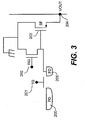
- FIG. 3 provides a single pixel schematic for this non-shared pinned photodiode structure of FIG. 2 .
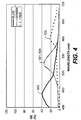
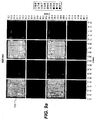
- FIG. 4 shows simulation results for QE for a prior art 1.1 ⁇ m pixel array with a Bayer pattern.
- the peak QE for the blue response curve 503 associated with the blue pixels 103 is 40%.
- the peak QE for the green response curves 501, 504 associated with the green pixels 101, 104 is 35%.
- the peak QE for the red response curve 502 associated with the red pixel 102 is 23%.
- the thickness of the dielectric spacer 221 layer is 0.5 ⁇ m. Increasing the dielectric spacer thickness 221 degrades performance resulting in lower peak QE and increased color crosstalk.
- US 2006/145223 provides an image sensor and a fabrication method thereof.
- the image sensor includes: a first photodiode formed in a substrate and receiving a first color; a second photodiode formed in the substrate apart from the first photodiode and receiving a second color with a wavelength longer than that of the first color; a third photodiode formed in the substrate apart from the first photodiode and the second photodiode and receiving a third color with a wavelength longer than that of the second color; and a passivation layer formed on the substrate and having different regional thicknesses whose magnitude increases in order of a first region of the passivation layer corresponding to a first color region, a second region of the passivation layer corresponding to a second color region and a third region of the passivation layer corresponding to a third color region.
- WO2008/017490A2 discloses an imager with a filter array formed of Fabry Perot filter elements.
- This object is achieved by adjusting optical path differences for each pixel in a color kernel such that for a specific wavelength the light intensity falling onto the image sensor interferes constructively near the surface of one pixel and destructively for the other pixels within the color kernel. For another specific wavelength, light interferes constructively near the surface of a second pixel and destructively for the other pixels within the color kernel.
- the present invention has the advantage of improving color crosstalk between adjacent pixels and increasing QE.
- optical path n ⁇ d , where n is the index of refraction and d is the thickness of the material through which the light is passing.
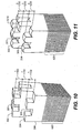
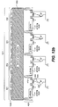
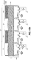
- FIG. 7 there is shown a portion of an image sensor array 401 of an image sensor of the first embodiment of the present invention. It is noted that, although the cross section only shows four pixels for simplicity, the image sensor array 401 typically includes thousands or millions of pixels. It is further noted that the image sensor array 401 is typically a part of an active pixel sensor as will be discussed in FIG. 19 .
- the image sensor array 401 includes a plurality of pixels 301 and 302 disposed in an active layer 420.
- the pixels 301 and 302 are preferably grouped together in a 2x2 array, hereinafter a color kernel, that repeats over the array as will be described in detail hereinbelow.
- Each pixel 301 and 302 includes a charge collection region, preferably a pinned photodiode 400, disposed slightly away from the surface of the active layer that receives the incident light 250.
- the configuration of polysilicon gates 401, 402, 403, and metal wires 404 opposite the illuminated side of the active layer 420 is called backside illumination.
- the pinned photodiode 400 collects charge in response to the incident light.
- the pinned photodiode 400 includes a pinning layer 412 beneath a doped region of opposite conductivity type disposed thereon.
- a photodiode may also be used as the charge collection region and front illumination be used as charge collection region, both of which are well known and will not be discussed herein.
- a transfer gate 401 When activated, a transfer gate 401 passes charge from the pinned photodiode 400 to a charge-to-voltage conversion region 405, preferably a floating diffusion, which converts charge to a voltage signal.
- a reset gate 402 is activated for resetting the floating diffusion 405 to a predetermined signal level.
- a transparent grating layer 300 with a varying thickness is disposed spanning the pixels 301 and 302 (and the pixels not shown in the drawing) for directing the incident light 250 into the active layer 420 as will be described in detail hereinbelow.
- the transparent layer may be made of either silicon dioxide, silicon nitride or a transparent organic material.
- the 2x2 color kernel 310 having the transparent layer overlaid thereon.
- the thickness of the transparent layer 300 (see FIG. 7 ) over each pixel 301, 302, 303, and 304 (see FIGS. 5 and 6 for all four pixels) in the color kernel 310 is different (Y, Z, W, and X). This creates four optical paths.
- the present invention in its preferred embodiment uses thickness to create the different optical paths, materials having different index of refractions may be used to create the different optical paths.
- the thickness of the silicon dioxide transparent layer 300 for Y, Z, W, and X are 2.5 ⁇ m, 3.0 ⁇ m, 1.5 ⁇ m, and 2.0 ⁇ m, respectively. Consequently, there are four optical paths created. Blue light constructively interferes just above pixel 303 and is effectively directed into this pixel. Likewise, green-blue light is directed into pixel 301, green-red light is directed into pixel 304, and red light is directed into pixel 302. It is noted that the repeating pattern of the transparent layer 300 is repeated for each kernel of pixels.
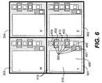
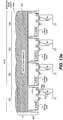
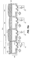
- FIG. 6 shows a more detailed plan view of the four pixels 301, 302, 303, and 304 within a color kernel 310 and the device components buried beneath the imager surface.
- These components include the photodiode 400, transfer gate 401, reset gate 402, source-follower 403, source-follower output 404, floating-diffusion 405, sidewall isolation 410, reset drain 413, and contacts 350 from the metal lines (not shown) to the gates 401, 402, 403, and source/drain implant regions 405, 413, 404.
- These device components are also illustrated in the cross-section of FIG. 7 .
- the optical stack is simply a transparent layer 300. Through this cross-section in FIG. 7 there are only two heights Y and Z.
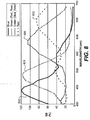
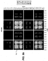
- FIG. 8 shows simulation results for QE for a 1.1 ⁇ m pixel array using the first embodiment of the present invention as describe by FIGS. 5-7 .
- the peak QE for the blue response curve 603 associated with the blue pixel 303 is 120%.
- the peak QE for the green/blue response curve 601 associated with the green/blue pixel 301 is 116%.
- the peak QE for the green/red response curve 604 associated with the green/red pixel 304 is 105%.
- the peak QE for the red response curve 604 associated with the red pixel 302 is 86%.
- the QE for a given wavelength can be greater than 100% for a given pixel because the optical paths are adjusted in such a way to take advantage of constructive and destructive interference.
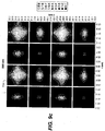
- FIGS. 9a-9d illustrate how constructive and destructive interference leads to QE curves with peaks greater than 100%. Shown are four plan view plots of the light intensity just above the silicon active layer 420 on the illuminated side for different wavelengths. For blue light (420 nm) most of the light intensity 703 is above pixel 303. Likewise, for green/blue light (470 nm) most of the light intensity 701 is above pixel 301. Likewise again, for green/red light (590 nm) most of the light intensity 704 is above pixel 304. Finally, for red light (650 nm) most of the light intensity 702 is above pixel 302.
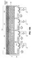
- FIG. 10 shows a 4x4 pixel cutaway of FIGS. 5-7 .
- the optical stack 300 on top of the active layer 420.
- the four pixels (301, 302, 303, and 304) within a single color kernel are identified, along with the ⁇ height differences 1050 between the four transparent pillars.
- the peak QE for the blue, green/blue, green/red, and red response curves (603, 601, 604, and 602) are at wavelengths of 440 nm, 485 nm, 585 nm, and 645 nm respectively. This is for normal incidence. Unfortunately, tilting the angle of the incoming light away from normal incidence increases the optical path differences for the different pixels. This changes the details of the constructive and destructive interference and results in slight differences for the wavelength at which the QE is a peak for the different response curves. The differences in peak position increase further with increasing tilt angle.
- the chief ray at the center of the pixel array is normal incidence; however, the chief ray angle for pixels near the edge of the array can exceed 30 degrees. Since the response curves depend on tilt angle, this leads to color shifts (hue shifts) across the image that are not always easy to correct.
- One method is to refine the binary optical path grating with more height differences, and optimize this refined system. This involves more etches to provide more possible heights in the transparent layer. This refinement also involves breaking the pixel into sub-pixel regions. For example, consider the case where there are eight possible heights and each pixel is broken up into sixteen-square subregions. With four pixels, this gives 512 degrees of freedom for the optical stack. Using numerical simulation, all cases can be modeled for a range of wavelengths, and the system optimized in such a way that there is good color separation for the four pixels, and the hue shifts are minimal.
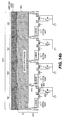
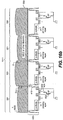
- FIG. 11 shows an optical path grating similar to the optical path grating of FIG. 11 where the optical path difference between pixels is ⁇ 1250 but there is also a microlens above each pixel 1210. This new structure will have better hue shift performance with changing tilt angle.
- FIGS. 12-16 illustrate a method for fabricating an optical path grating with curved surfaces in the shape of a microlens as in FIG. 11 . It is noted that FIGS. 12-16 describe ⁇ changes referenced by numerals not directly shown in FIGS. 12-16 but are shown in FIGS. 10, 11 , 17 and/or 18. The following described procedure requires fewer lithography steps than that of a Bayer CFA.
- FIGS. 12a-12b show two cross-sections of four pixels each, one through pixels 303 and 304 of the color kernel, the other through pixels 301 and 302 of the color kernel. Fabrication of the devices within the active layer 420 is complete, and the back illuminated imager thinned.
- Silicon dioxide or some other transparent layer 300 of thickness greater than D has been grown or deposited on the illuminated side of the active layer 420.
- One top of the layer 300 is a patterned microlens array 1025.
- There are numbers of methods for fabricating this microlens array including microgap patterning and reflow and gray scale photolithography.
- FIGS. 13a-13b show the silicon dioxide layer 300 after a 1:1 directional etch that transfers the microlens surface into the transparent layer material.
- the thickness of layer 300 at the edge of the microlens is D.
- a resist layer 1020 is applied to a portion of the image array and patterned so that pixels 301 and 302 are covered with resist 1020, and the pattern leaves exposed the transparent layer 300 within pixels 303 and 304.
- the exposed transparent layer 300 is etched a thickness of 2 ⁇ 1030.
- FIGS. 14a-14b show both cross-sections after a thickness of 2 ⁇ 1030 of the transparent layer is etched and removed as discussed in the previous paragraph. The resist 1020 is then removed.
- FIGS. 15a-15b illustrate the next step in the process after the patterned resist 1020 for the first etch is removed as discussed in the previous paragraph.
- a second resist layer 1040 is applied to the image array and patterned. This pattern exposes the transparent layer 300 within pixels 301, 303 and covers the transparent layer 300 within pixels 302 and 304. The exposed transparent layer 300 is etched and removed.
- FIGS. 16a-16b show both cross-sections after a thickness of ⁇ 1050 of the transparent layer is etched and removed as discussed in the preceding paragraph.
- the resist 1040 (of FIG. 15b ) is removed.
- the final thicknesses of the transparent layer 300 are D, D- ⁇ , D-2 ⁇ , and D-3 ⁇ for pixels 302, 301, 304, and 303 respectively.
- the optical path grating in FIG. 11 will have superior hue shift performance to the optical path grating in FIG 10 , however, for steeper and steeper angles, the highest pillar of transparent material (pixel 302 ) casts shadows on the shorter pillars (pixels 301, 304, and 303 ) since the material is not 100% transparent. This shadowing leads to hue shifts, the root cause of which is not variations in optical path length, but instead a reduction in light intensity over the shorter pixels.
- FIG. 17 illustrates a way to minimize the hue shifts due to shadowing and optical path length differences.
- a second transparent material 1320 is inserted between the original optical path grating 300 and the microlens 1430.
- the microlens array 1430 is placed on top of the planer surface of layer 1320. The planar microlens array eliminates problems due to shadowing.
- FIG. 18 shows a structure similar to FIG. 17 except the size of the microlens 1530 equals the size of the color kernel and not the individual pixel (301, 302, 303, and 304). This has the advantage of focusing the light bundle from each microlens 1530 through each optical grating block (301, 302, 303, and 304) reducing hue shift even more.
- FIG. 19 is a block diagram of an imaging system that can be used with the image sensor array 401 of an example to understand the present invention.
- Imaging system 1200 includes digital camera phone 1202 and computing device 1204.
- Digital camera phone 1202 is an example of an image capture device that can use an image sensor incorporating the present invention.
- Other types of image capture devices can also be used with the present invention, such as, for example, digital still cameras and digital video camcorders.
- Digital camera phone 1202 is a portable, handheld, battery-operated device in an embodiment in accordance with the invention.
- Digital camera phone 1202 produces digital images that are stored in memory 1206, which can be, for example, an internal Flash EPROM memory or a removable memory card.
- memory 1206 can be, for example, an internal Flash EPROM memory or a removable memory card.
- Other types of digital image storage media such as magnetic hard drives, magnetic tape, or optical disks, can alternatively be used to implement memory 1206.
- Digital camera phone 1202 uses lens 1208 to focus light from a scene (not shown) onto image sensor array 401 of active pixel sensor 1212.
- Image sensor array 401 provides color image information using the Bayer color filter pattern in an example being useful to understand the present invention.
- Image sensor array 401 is controlled by timing generator 1214, which also controls flash 1216 in order to illuminate the scene when the ambient illumination is low.
- the analog output signals output from the image sensor array 410 are amplified and converted to digital data by analog-to-digital (A/D) converter circuit 1218.
- the digital data are stored in buffer memory 1220 and subsequently processed by digital processor 1222.
- Digital processor 1222 is controlled by the firmware stored in firmware memory 1224, which can be flash EPROM memory.
- Digital processor 1222 includes real-time clock 1226, which keeps the date and time even when digital camera phone 1202 and digital processor 1222 are in a low power state.
- the processed digital image files are stored in memory 1206.
- Memory 1206 can also store other types of data, such as, for example, music files (e.g. MP3 files), ring tones, phone numbers, calendars, and to-do lists.
- digital camera phone 1202 captures still images.
- Digital processor 1222 performs color interpolation followed by color and tone correction, in order to produce rendered sRGB image data.
- the rendered sRGB image data are then compressed and stored as an image file in memory 1206.
- the image data can be compressed pursuant to the JPEG format, which uses the known "Exif' image format.
- This format includes an Exif application segment that stores particular image metadata using various TIFF tags. Separate TIFF tags can be used, for example, to store the date and time the picture was captured, the lens f/number and other camera settings, and to store image captions.
- Digital processor 1222 produces different image sizes that are selected by the user in; an example.
- One such size is the low-resolution "thumbnail" size image.
- Generating thumbnail-size images is described in commonly assigned U.S. Patent No. 5,164,831 , entitled “Electronic Still Camera Providing Multi-Format Storage Of Full And Reduced Resolution Images” to Kuchta, et al.
- the thumbnail image is stored in RAM memory 1228 and supplied to display 1230, which can be, for example, an active matrix LCD or organic light emitting diode (OLED).
- Generating thumbnail size images allows the captured images to be reviewed quickly on color display 1230.
- digital camera phone 1202 also produces and stores video clips.
- a video clip is produced by summing multiple pixels of image sensor array 410 together (e.g. summing pixels of the same color within each 4 column x 4 row area of the image sensor array 410 ) to create a lower resolution video image frame.
- the video image frames are read from image sensor array 410 at regular intervals, for example, using a 15 frame per second readout rate.
- Audio codec 1232 is connected to digital processor 1222 and receives an audio signal from microphone (Mic) 1234. Audio codec 1232 also provides an audio signal to speaker 1236. These components are used both for telephone conversations and to record and playback an audio track, along with a video sequence or still image.
- Speaker 1236 is also used to inform the user of an incoming phone call in an example. This can be done using a standard ring tone stored in firmware memory 1224, or by using a custom ring-tone downloaded from mobile phone network 1238 and stored in memory 1206.
- a vibration device (not shown) can be used to provide a silent (e.g. non-audible) notification of an incoming phone call.
- Digital processor 1222 is connected to wireless modem 1240, which enables digital camera phone 1202 to transmit and receive information via radio frequency (RF) channel 1242.
- Wireless modem 1240 communicates with mobile phone network 1238 using another RF link (not shown), such as a 3GSM network.
- Mobile phone network 1238 communicates with photo service provider 1244, which stores digital images uploaded from digital camera phone 1202. Other devices, including computing device 1204, access these images via the Internet 1246.
- Mobile phone network 1238 also connects to a standard telephone network (not shown) in order to provide normal telephone service in an example.
- a graphical user interface (not shown) is displayed on display 1230 and controlled by user controls 1248.
- User controls 1248 include dedicated push buttons (e.g. a telephone keypad) to dial a phone number, a control to set the mode (e.g. "phone” mode, "calendar” mode” “camera” mode), a joystick controller that includes 4-way control (up, down, left, right) and a push-button center “OK” or "select” switch, in embodiments in accordance with the invention.
- Dock 1251 recharges the batteries (not shown) in digital camera phone 1202.
- Dock 1251 connects digital camera phone 1202 to computing device 1204 via dock interface 1252.
- Dock interface 1252 is implemented as wired interface, such as a USB interface, in an example.
- dock interface 1252 is implemented as a wireless interface, such as a Bluetooth or an IEEE 802.11b wireless. interface.
- Dock interface 1252 is used to download images from memory 1206 to computing device 1204. Dock interface 1252 is also used to transfer calendar information from computing device 1204 to memory 1206 in digital camera phone 1202.
Landscapes
- Engineering & Computer Science (AREA)
- Multimedia (AREA)
- Signal Processing (AREA)
- Solid State Image Pick-Up Elements (AREA)
- Transforming Light Signals Into Electric Signals (AREA)
- Color Television Image Signal Generators (AREA)
Applications Claiming Priority (2)
| Application Number | Priority Date | Filing Date | Title |
|---|---|---|---|
| US12/269,907 US8400537B2 (en) | 2008-11-13 | 2008-11-13 | Image sensors having gratings for color separation |
| PCT/US2009/005915 WO2010056285A1 (en) | 2008-11-13 | 2009-10-30 | Image sensors having gratings for color separation |
Publications (2)
| Publication Number | Publication Date |
|---|---|
| EP2347443A1 EP2347443A1 (en) | 2011-07-27 |
| EP2347443B1 true EP2347443B1 (en) | 2017-04-12 |
Family
ID=41510937
Family Applications (1)
| Application Number | Title | Priority Date | Filing Date |
|---|---|---|---|
| EP09745158.7A Active EP2347443B1 (en) | 2008-11-13 | 2009-10-30 | Image sensors having gratings for color separation |
Country Status (7)
Families Citing this family (41)
| Publication number | Priority date | Publication date | Assignee | Title |
|---|---|---|---|---|
| US7057256B2 (en) | 2001-05-25 | 2006-06-06 | President & Fellows Of Harvard College | Silicon-based visible and near-infrared optoelectric devices |
| US7442629B2 (en) | 2004-09-24 | 2008-10-28 | President & Fellows Of Harvard College | Femtosecond laser-induced formation of submicrometer spikes on a semiconductor substrate |
| US9911781B2 (en) | 2009-09-17 | 2018-03-06 | Sionyx, Llc | Photosensitive imaging devices and associated methods |
| US9673243B2 (en) | 2009-09-17 | 2017-06-06 | Sionyx, Llc | Photosensitive imaging devices and associated methods |
| US8692198B2 (en) | 2010-04-21 | 2014-04-08 | Sionyx, Inc. | Photosensitive imaging devices and associated methods |
| EP2583312A2 (en) | 2010-06-18 | 2013-04-24 | Sionyx, Inc. | High speed photosensitive devices and associated methods |
| US9496308B2 (en) * | 2011-06-09 | 2016-11-15 | Sionyx, Llc | Process module for increasing the response of backside illuminated photosensitive imagers and associated methods |
| US9419161B2 (en) * | 2011-06-24 | 2016-08-16 | Boly Media Communications (Shenzhen) Co., Ltd. | Hybrid multi-spectrum photosensitive pixel group, photosensitive device, and photosensitive system |
| EP2732402A2 (en) | 2011-07-13 | 2014-05-21 | Sionyx, Inc. | Biometric imaging devices and associated methods |
| JP5864990B2 (ja) | 2011-10-03 | 2016-02-17 | キヤノン株式会社 | 固体撮像装置およびカメラ |
| KR20140112012A (ko) * | 2012-01-12 | 2014-09-22 | 휴렛-팩커드 디벨롭먼트 컴퍼니, 엘.피. | 집적된 서브-파장 격자 시스템 |
| US9064764B2 (en) | 2012-03-22 | 2015-06-23 | Sionyx, Inc. | Pixel isolation elements, devices, and associated methods |
| JP6231741B2 (ja) | 2012-12-10 | 2017-11-15 | キヤノン株式会社 | 固体撮像装置およびその製造方法 |
| US9762830B2 (en) | 2013-02-15 | 2017-09-12 | Sionyx, Llc | High dynamic range CMOS image sensor having anti-blooming properties and associated methods |
| US9971078B2 (en) * | 2013-03-05 | 2018-05-15 | Rambus Inc. | Phase gratings with odd symmetry for high-resolution lensless optical sensing |
| US9110240B2 (en) * | 2013-03-05 | 2015-08-18 | Rambus Inc. | Phase gratings with odd symmetry for high-resolution lensed and lensless optical sensing |
| WO2014151093A1 (en) | 2013-03-15 | 2014-09-25 | Sionyx, Inc. | Three dimensional imaging utilizing stacked imager devices and associated methods |
| US9209345B2 (en) | 2013-06-29 | 2015-12-08 | Sionyx, Inc. | Shallow trench textured regions and associated methods |
| US9515113B2 (en) * | 2013-08-27 | 2016-12-06 | Rambus Inc. | Optical sensing of nearby scenes with tessellated phase anti-symmetric gratings |
| WO2015157097A1 (en) * | 2014-04-09 | 2015-10-15 | Rambus Inc. | Low-power image change detector |
| KR102219704B1 (ko) | 2014-06-13 | 2021-02-24 | 삼성전자주식회사 | 색분리 소자 어레이, 상기 색분리 소자 어레이를 포함하는 이미지 센서, 및 상기 색분리 소자 어레이를 포함하는 촬상 장치 |
| US9761730B2 (en) | 2014-10-29 | 2017-09-12 | Semiconductor Energy Laboratory Co., Ltd. | Imaging device and electronic device |
| WO2016118968A1 (en) * | 2015-01-23 | 2016-07-28 | Dartmouth College | Multi-junction pixel image sensor with dielectric reflector between photo detection layers |
| US10761323B2 (en) | 2015-03-04 | 2020-09-01 | Nippon Seiki Co., Ltd. | Lens array and image projection device |
| CN104867951B (zh) * | 2015-04-23 | 2018-05-04 | 豪威科技(上海)有限公司 | 一种背照式传感器芯片及其制造方法 |
| US10284825B2 (en) | 2015-09-08 | 2019-05-07 | Rambus Inc. | Systems with integrated refractive and diffractive optics |
| KR102465995B1 (ko) * | 2015-09-30 | 2022-11-25 | 삼성전자주식회사 | 색분할기 구조와 그 제조방법, 색분할기 구조를 포함하는 이미지센서 및 이미지센서를 포함하는 광학장치 |
| FR3043495A1 (fr) * | 2015-11-09 | 2017-05-12 | St Microelectronics Crolles 2 Sas | Capteur d'images a obturation globale |
| CN105428377A (zh) * | 2015-11-11 | 2016-03-23 | 武汉新芯集成电路制造有限公司 | 一种cmos影像传感器 |
| KR102524400B1 (ko) * | 2016-07-04 | 2023-04-24 | 에스케이하이닉스 주식회사 | 하나의 컬러 필터 및 하나의 마이크로렌즈를 공유하는 다수 개의 포토다이오드들을 갖는 이미지 센서 |
| CN108174059B (zh) * | 2016-12-08 | 2021-04-13 | 松下知识产权经营株式会社 | 摄像装置 |
| JP6975897B2 (ja) * | 2016-12-27 | 2021-12-01 | パナソニックIpマネジメント株式会社 | 画像生成装置及び撮像装置 |
| US10578870B2 (en) | 2017-07-26 | 2020-03-03 | Magic Leap, Inc. | Exit pupil expander |
| US10468448B2 (en) * | 2017-11-30 | 2019-11-05 | Taiwan Semiconductor Manufacturing Company Ltd. | Semiconductor image sensor and method for forming the same |
| CN112930490A (zh) * | 2018-10-22 | 2021-06-08 | ams传感器亚洲私人有限公司 | 结构化照明装置 |
| EP3981143A4 (en) | 2019-06-05 | 2023-07-26 | Airy3d Inc. | ILLUMINATED FIELD IMAGING DEVICE AND METHOD FOR 3D SCANNING |
| CN111427107B (zh) * | 2020-04-07 | 2022-02-15 | 上海冠众光学科技有限公司 | 一种衍射光学元件取值模型、衍射光学元件及其制作方法 |
| CN112616008B (zh) * | 2020-12-31 | 2022-08-30 | 维沃移动通信有限公司 | 电子设备及其摄像模组 |
| CN113554578B (zh) * | 2021-07-23 | 2024-05-31 | 奥比中光科技集团股份有限公司 | 一种光谱图像的确定方法、装置、终端和存储介质 |
| WO2024147826A1 (en) * | 2023-01-05 | 2024-07-11 | Transformative Optics Corporation | Color image sensors, methods and systems |
| WO2024182612A1 (en) * | 2023-03-02 | 2024-09-06 | Transformative Optics Corporation | Color image sensors, methods and systems |
Family Cites Families (32)
| Publication number | Priority date | Publication date | Assignee | Title |
|---|---|---|---|---|
| US4506949A (en) * | 1983-05-27 | 1985-03-26 | Rca Corporation | Diffractive color separation filter |
| US5164831A (en) * | 1990-03-15 | 1992-11-17 | Eastman Kodak Company | Electronic still camera providing multi-format storage of full and reduced resolution images |
| JP2601148B2 (ja) * | 1993-07-23 | 1997-04-16 | 日本電気株式会社 | 固体撮像装置 |
| JP3620237B2 (ja) * | 1997-09-29 | 2005-02-16 | ソニー株式会社 | 固体撮像素子 |
| US6300612B1 (en) * | 1998-02-02 | 2001-10-09 | Uniax Corporation | Image sensors made from organic semiconductors |
| JPH11284158A (ja) * | 1998-03-27 | 1999-10-15 | Sony Corp | 固体撮像素子と固体撮像素子の製造方法 |
| FR2781929B1 (fr) * | 1998-07-28 | 2002-08-30 | St Microelectronics Sa | Capteur d'image a reseau de photodiodes |
| JP2001309395A (ja) * | 2000-04-21 | 2001-11-02 | Sony Corp | 固体撮像素子及びその製造方法 |
| US6556349B2 (en) | 2000-12-27 | 2003-04-29 | Honeywell International Inc. | Variable focal length micro lens array field curvature corrector |
| JP3759435B2 (ja) * | 2001-07-11 | 2006-03-22 | ソニー株式会社 | X−yアドレス型固体撮像素子 |
| US7199931B2 (en) * | 2003-10-09 | 2007-04-03 | Micron Technology, Inc. | Gapless microlens array and method of fabrication |
| CN100449764C (zh) * | 2003-11-18 | 2009-01-07 | 松下电器产业株式会社 | 光电探测器 |
| JP4181487B2 (ja) * | 2003-11-28 | 2008-11-12 | 松下電器産業株式会社 | 固体撮像装置とその製造方法 |
| KR100680386B1 (ko) | 2004-01-15 | 2007-02-08 | 마츠시타 덴끼 산교 가부시키가이샤 | 고체촬상장치, 고체촬상장치의 제조방법 및 이를 이용한카메라 |
| US7068432B2 (en) * | 2004-07-27 | 2006-06-27 | Micron Technology, Inc. | Controlling lens shape in a microlens array |
| JP4507769B2 (ja) * | 2004-08-31 | 2010-07-21 | ソニー株式会社 | 固体撮像素子、カメラモジュール及び電子機器モジュール |
| KR100672699B1 (ko) * | 2004-12-29 | 2007-01-22 | 동부일렉트로닉스 주식회사 | 씨모스 이미지 센서의 제조방법 |
| KR100658930B1 (ko) * | 2004-12-30 | 2006-12-15 | 매그나칩 반도체 유한회사 | 칼라별 초점 거리 조절이 가능한 이미지센서 및 그 제조방법 |
| US7560684B2 (en) * | 2005-03-23 | 2009-07-14 | Panasonic Corporation | On-vehicle imaging device |
| JP4456040B2 (ja) * | 2005-06-17 | 2010-04-28 | パナソニック株式会社 | 固体撮像素子 |
| US7736939B2 (en) * | 2005-07-07 | 2010-06-15 | United Microelectronics Corp. | Method for forming microlenses of different curvatures and fabricating process of solid-state image sensor |
| US7522341B2 (en) * | 2005-07-12 | 2009-04-21 | Micron Technology, Inc. | Sharing of microlenses among pixels in image sensors |
| JP2007103401A (ja) * | 2005-09-30 | 2007-04-19 | Matsushita Electric Ind Co Ltd | 撮像装置及び画像処理装置 |
| JP2007109801A (ja) * | 2005-10-12 | 2007-04-26 | Sumitomo Electric Ind Ltd | 固体撮像装置とその製造方法 |
| JP2008005383A (ja) * | 2006-06-26 | 2008-01-10 | Matsushita Electric Ind Co Ltd | 撮像装置及びイメージセンサ |
| US7505206B2 (en) * | 2006-07-10 | 2009-03-17 | Taiwan Semiconductor Manufacturing Company | Microlens structure for improved CMOS image sensor sensitivity |
| FR2904432B1 (fr) | 2006-07-25 | 2008-10-24 | Commissariat Energie Atomique | Structure matricielle de filtrage optique et capteur d'images associe |
| JP2008041779A (ja) * | 2006-08-02 | 2008-02-21 | Matsushita Electric Ind Co Ltd | 固体撮像装置 |
| US8629986B2 (en) | 2006-08-09 | 2014-01-14 | Biozoom Technologies, Inc. | Optical filter and method for the production of the same, and device for the examination of electromagnetic radiation |
| US8610806B2 (en) * | 2006-08-28 | 2013-12-17 | Micron Technology, Inc. | Color filter array, imagers and systems having same, and methods of fabrication and use thereof |
| KR20080049186A (ko) * | 2006-11-30 | 2008-06-04 | 동부일렉트로닉스 주식회사 | 이미지 센서 및 그 제조방법 |
| CN102007593B (zh) | 2008-04-18 | 2013-01-02 | Nxp股份有限公司 | 集成电路制造方法 |
-
2008
- 2008-11-13 US US12/269,907 patent/US8400537B2/en active Active
-
2009
- 2009-10-30 KR KR1020117012394A patent/KR101593258B1/ko active Active
- 2009-10-30 CN CN200980142487.4A patent/CN102197486B/zh active Active
- 2009-10-30 EP EP09745158.7A patent/EP2347443B1/en active Active
- 2009-10-30 WO PCT/US2009/005915 patent/WO2010056285A1/en active Application Filing
- 2009-10-30 JP JP2011536307A patent/JP5676462B2/ja active Active
- 2009-11-12 TW TW098138493A patent/TWI476908B/zh active
Non-Patent Citations (1)
| Title |
|---|
| None * |
Also Published As
| Publication number | Publication date |
|---|---|
| EP2347443A1 (en) | 2011-07-27 |
| TW201029166A (en) | 2010-08-01 |
| US20100118172A1 (en) | 2010-05-13 |
| JP5676462B2 (ja) | 2015-02-25 |
| KR20110082182A (ko) | 2011-07-18 |
| US8400537B2 (en) | 2013-03-19 |
| TWI476908B (zh) | 2015-03-11 |
| WO2010056285A1 (en) | 2010-05-20 |
| CN102197486B (zh) | 2015-02-18 |
| CN102197486A (zh) | 2011-09-21 |
| KR101593258B1 (ko) | 2016-02-11 |
| JP2012508977A (ja) | 2012-04-12 |
Similar Documents
| Publication | Publication Date | Title |
|---|---|---|
| EP2347443B1 (en) | Image sensors having gratings for color separation | |
| US8049256B2 (en) | Active pixel sensor having a sensor wafer connected to a support circuit wafer | |
| EP2324506B1 (en) | High gain read circuit for 3d integrated pixel | |
| JP4192867B2 (ja) | 物理情報取得装置、複数の単位構成要素が配列されてなる物理量分布検知の半導体装置、並びに半導体装置の製造方法 | |
| TWI442555B (zh) | 具有二晶圓之主動式像素感測器 | |
| KR20140113633A (ko) | 고체 촬상 장치, 고체 촬상 장치의 제조 방법, 및 전자 기기 | |
| WO2009154713A1 (en) | High dynamic range image sensor | |
| KR101438710B1 (ko) | 넓은 애퍼처 이미지 센서 픽셀 | |
| WO2009148563A1 (en) | Image sensors with improved angle response | |
| CN100555650C (zh) | 固态成像器件和成像设备 | |
| JP4662966B2 (ja) | 撮像装置 | |
| JP2009200324A (ja) | 半導体装置の製造方法および電子情報機器 |
Legal Events
| Date | Code | Title | Description |
|---|---|---|---|
| PUAI | Public reference made under article 153(3) epc to a published international application that has entered the european phase |
Free format text: ORIGINAL CODE: 0009012 |
|
| 17P | Request for examination filed |
Effective date: 20110525 |
|
| AK | Designated contracting states |
Kind code of ref document: A1 Designated state(s): AT BE BG CH CY CZ DE DK EE ES FI FR GB GR HR HU IE IS IT LI LT LU LV MC MK MT NL NO PL PT RO SE SI SK SM TR |
|
| AX | Request for extension of the european patent |
Extension state: AL BA RS |
|
| RAP1 | Party data changed (applicant data changed or rights of an application transferred) |
Owner name: OMNIVISION TECHNOLOGIES, INC. |
|
| DAX | Request for extension of the european patent (deleted) | ||
| 17Q | First examination report despatched |
Effective date: 20150925 |
|
| GRAP | Despatch of communication of intention to grant a patent |
Free format text: ORIGINAL CODE: EPIDOSNIGR1 |
|
| INTG | Intention to grant announced |
Effective date: 20161206 |
|
| GRAS | Grant fee paid |
Free format text: ORIGINAL CODE: EPIDOSNIGR3 |
|
| GRAA | (expected) grant |
Free format text: ORIGINAL CODE: 0009210 |
|
| AK | Designated contracting states |
Kind code of ref document: B1 Designated state(s): AT BE BG CH CY CZ DE DK EE ES FI FR GB GR HR HU IE IS IT LI LT LU LV MC MK MT NL NO PL PT RO SE SI SK SM TR |
|
| REG | Reference to a national code |
Ref country code: GB Ref legal event code: FG4D |
|
| REG | Reference to a national code |
Ref country code: CH Ref legal event code: EP |
|
| REG | Reference to a national code |
Ref country code: IE Ref legal event code: FG4D |
|
| REG | Reference to a national code |
Ref country code: AT Ref legal event code: REF Ref document number: 884670 Country of ref document: AT Kind code of ref document: T Effective date: 20170515 |
|
| REG | Reference to a national code |
Ref country code: DE Ref legal event code: R096 Ref document number: 602009045387 Country of ref document: DE |
|
| REG | Reference to a national code |
Ref country code: NL Ref legal event code: MP Effective date: 20170412 |
|
| REG | Reference to a national code |
Ref country code: LT Ref legal event code: MG4D Ref country code: FR Ref legal event code: PLFP Year of fee payment: 9 |
|
| REG | Reference to a national code |
Ref country code: AT Ref legal event code: MK05 Ref document number: 884670 Country of ref document: AT Kind code of ref document: T Effective date: 20170412 |
|
| PG25 | Lapsed in a contracting state [announced via postgrant information from national office to epo] |
Ref country code: NL Free format text: LAPSE BECAUSE OF FAILURE TO SUBMIT A TRANSLATION OF THE DESCRIPTION OR TO PAY THE FEE WITHIN THE PRESCRIBED TIME-LIMIT Effective date: 20170412 |
|
| PG25 | Lapsed in a contracting state [announced via postgrant information from national office to epo] |
Ref country code: ES Free format text: LAPSE BECAUSE OF FAILURE TO SUBMIT A TRANSLATION OF THE DESCRIPTION OR TO PAY THE FEE WITHIN THE PRESCRIBED TIME-LIMIT Effective date: 20170412 Ref country code: LT Free format text: LAPSE BECAUSE OF FAILURE TO SUBMIT A TRANSLATION OF THE DESCRIPTION OR TO PAY THE FEE WITHIN THE PRESCRIBED TIME-LIMIT Effective date: 20170412 Ref country code: HR Free format text: LAPSE BECAUSE OF FAILURE TO SUBMIT A TRANSLATION OF THE DESCRIPTION OR TO PAY THE FEE WITHIN THE PRESCRIBED TIME-LIMIT Effective date: 20170412 Ref country code: NO Free format text: LAPSE BECAUSE OF FAILURE TO SUBMIT A TRANSLATION OF THE DESCRIPTION OR TO PAY THE FEE WITHIN THE PRESCRIBED TIME-LIMIT Effective date: 20170712 Ref country code: AT Free format text: LAPSE BECAUSE OF FAILURE TO SUBMIT A TRANSLATION OF THE DESCRIPTION OR TO PAY THE FEE WITHIN THE PRESCRIBED TIME-LIMIT Effective date: 20170412 Ref country code: GR Free format text: LAPSE BECAUSE OF FAILURE TO SUBMIT A TRANSLATION OF THE DESCRIPTION OR TO PAY THE FEE WITHIN THE PRESCRIBED TIME-LIMIT Effective date: 20170713 Ref country code: FI Free format text: LAPSE BECAUSE OF FAILURE TO SUBMIT A TRANSLATION OF THE DESCRIPTION OR TO PAY THE FEE WITHIN THE PRESCRIBED TIME-LIMIT Effective date: 20170412 |
|
| PG25 | Lapsed in a contracting state [announced via postgrant information from national office to epo] |
Ref country code: BG Free format text: LAPSE BECAUSE OF FAILURE TO SUBMIT A TRANSLATION OF THE DESCRIPTION OR TO PAY THE FEE WITHIN THE PRESCRIBED TIME-LIMIT Effective date: 20170712 Ref country code: PL Free format text: LAPSE BECAUSE OF FAILURE TO SUBMIT A TRANSLATION OF THE DESCRIPTION OR TO PAY THE FEE WITHIN THE PRESCRIBED TIME-LIMIT Effective date: 20170412 Ref country code: SE Free format text: LAPSE BECAUSE OF FAILURE TO SUBMIT A TRANSLATION OF THE DESCRIPTION OR TO PAY THE FEE WITHIN THE PRESCRIBED TIME-LIMIT Effective date: 20170412 Ref country code: IS Free format text: LAPSE BECAUSE OF FAILURE TO SUBMIT A TRANSLATION OF THE DESCRIPTION OR TO PAY THE FEE WITHIN THE PRESCRIBED TIME-LIMIT Effective date: 20170812 Ref country code: LV Free format text: LAPSE BECAUSE OF FAILURE TO SUBMIT A TRANSLATION OF THE DESCRIPTION OR TO PAY THE FEE WITHIN THE PRESCRIBED TIME-LIMIT Effective date: 20170412 |
|
| REG | Reference to a national code |
Ref country code: DE Ref legal event code: R097 Ref document number: 602009045387 Country of ref document: DE |
|
| PG25 | Lapsed in a contracting state [announced via postgrant information from national office to epo] |
Ref country code: DK Free format text: LAPSE BECAUSE OF FAILURE TO SUBMIT A TRANSLATION OF THE DESCRIPTION OR TO PAY THE FEE WITHIN THE PRESCRIBED TIME-LIMIT Effective date: 20170412 Ref country code: CZ Free format text: LAPSE BECAUSE OF FAILURE TO SUBMIT A TRANSLATION OF THE DESCRIPTION OR TO PAY THE FEE WITHIN THE PRESCRIBED TIME-LIMIT Effective date: 20170412 Ref country code: EE Free format text: LAPSE BECAUSE OF FAILURE TO SUBMIT A TRANSLATION OF THE DESCRIPTION OR TO PAY THE FEE WITHIN THE PRESCRIBED TIME-LIMIT Effective date: 20170412 Ref country code: RO Free format text: LAPSE BECAUSE OF FAILURE TO SUBMIT A TRANSLATION OF THE DESCRIPTION OR TO PAY THE FEE WITHIN THE PRESCRIBED TIME-LIMIT Effective date: 20170412 Ref country code: SK Free format text: LAPSE BECAUSE OF FAILURE TO SUBMIT A TRANSLATION OF THE DESCRIPTION OR TO PAY THE FEE WITHIN THE PRESCRIBED TIME-LIMIT Effective date: 20170412 |
|
| PLBE | No opposition filed within time limit |
Free format text: ORIGINAL CODE: 0009261 |
|
| STAA | Information on the status of an ep patent application or granted ep patent |
Free format text: STATUS: NO OPPOSITION FILED WITHIN TIME LIMIT |
|
| PG25 | Lapsed in a contracting state [announced via postgrant information from national office to epo] |
Ref country code: SM Free format text: LAPSE BECAUSE OF FAILURE TO SUBMIT A TRANSLATION OF THE DESCRIPTION OR TO PAY THE FEE WITHIN THE PRESCRIBED TIME-LIMIT Effective date: 20170412 Ref country code: IT Free format text: LAPSE BECAUSE OF FAILURE TO SUBMIT A TRANSLATION OF THE DESCRIPTION OR TO PAY THE FEE WITHIN THE PRESCRIBED TIME-LIMIT Effective date: 20170412 |
|
| 26N | No opposition filed |
Effective date: 20180115 |
|
| PG25 | Lapsed in a contracting state [announced via postgrant information from national office to epo] |
Ref country code: SI Free format text: LAPSE BECAUSE OF FAILURE TO SUBMIT A TRANSLATION OF THE DESCRIPTION OR TO PAY THE FEE WITHIN THE PRESCRIBED TIME-LIMIT Effective date: 20170412 Ref country code: MC Free format text: LAPSE BECAUSE OF FAILURE TO SUBMIT A TRANSLATION OF THE DESCRIPTION OR TO PAY THE FEE WITHIN THE PRESCRIBED TIME-LIMIT Effective date: 20170412 |
|
| REG | Reference to a national code |
Ref country code: IE Ref legal event code: MM4A |
|
| PG25 | Lapsed in a contracting state [announced via postgrant information from national office to epo] |
Ref country code: LU Free format text: LAPSE BECAUSE OF NON-PAYMENT OF DUE FEES Effective date: 20171030 |
|
| REG | Reference to a national code |
Ref country code: BE Ref legal event code: MM Effective date: 20171031 |
|
| PG25 | Lapsed in a contracting state [announced via postgrant information from national office to epo] |
Ref country code: BE Free format text: LAPSE BECAUSE OF NON-PAYMENT OF DUE FEES Effective date: 20171031 |
|
| REG | Reference to a national code |
Ref country code: FR Ref legal event code: PLFP Year of fee payment: 10 |
|
| PG25 | Lapsed in a contracting state [announced via postgrant information from national office to epo] |
Ref country code: MT Free format text: LAPSE BECAUSE OF NON-PAYMENT OF DUE FEES Effective date: 20171030 |
|
| PG25 | Lapsed in a contracting state [announced via postgrant information from national office to epo] |
Ref country code: IE Free format text: LAPSE BECAUSE OF NON-PAYMENT OF DUE FEES Effective date: 20171030 |
|
| PG25 | Lapsed in a contracting state [announced via postgrant information from national office to epo] |
Ref country code: HU Free format text: LAPSE BECAUSE OF FAILURE TO SUBMIT A TRANSLATION OF THE DESCRIPTION OR TO PAY THE FEE WITHIN THE PRESCRIBED TIME-LIMIT; INVALID AB INITIO Effective date: 20091030 |
|
| PG25 | Lapsed in a contracting state [announced via postgrant information from national office to epo] |
Ref country code: CY Free format text: LAPSE BECAUSE OF NON-PAYMENT OF DUE FEES Effective date: 20170412 |
|
| PG25 | Lapsed in a contracting state [announced via postgrant information from national office to epo] |
Ref country code: MK Free format text: LAPSE BECAUSE OF FAILURE TO SUBMIT A TRANSLATION OF THE DESCRIPTION OR TO PAY THE FEE WITHIN THE PRESCRIBED TIME-LIMIT Effective date: 20170412 |
|
| PG25 | Lapsed in a contracting state [announced via postgrant information from national office to epo] |
Ref country code: TR Free format text: LAPSE BECAUSE OF FAILURE TO SUBMIT A TRANSLATION OF THE DESCRIPTION OR TO PAY THE FEE WITHIN THE PRESCRIBED TIME-LIMIT Effective date: 20170412 |
|
| PG25 | Lapsed in a contracting state [announced via postgrant information from national office to epo] |
Ref country code: PT Free format text: LAPSE BECAUSE OF FAILURE TO SUBMIT A TRANSLATION OF THE DESCRIPTION OR TO PAY THE FEE WITHIN THE PRESCRIBED TIME-LIMIT Effective date: 20170412 |
|
| P01 | Opt-out of the competence of the unified patent court (upc) registered |
Effective date: 20230418 |
|
| PGFP | Annual fee paid to national office [announced via postgrant information from national office to epo] |
Ref country code: GB Payment date: 20240912 Year of fee payment: 16 |
|
| PGFP | Annual fee paid to national office [announced via postgrant information from national office to epo] |
Ref country code: FR Payment date: 20240913 Year of fee payment: 16 |
|
| REG | Reference to a national code |
Ref country code: DE Ref legal event code: R079 Ref document number: 602009045387 Country of ref document: DE Free format text: PREVIOUS MAIN CLASS: H01L0027146000 Ipc: H10F0039180000 |
|
| PGFP | Annual fee paid to national office [announced via postgrant information from national office to epo] |
Ref country code: DE Payment date: 20240913 Year of fee payment: 16 |
|
| PGFP | Annual fee paid to national office [announced via postgrant information from national office to epo] |
Ref country code: CH Payment date: 20241101 Year of fee payment: 16 |