EP2343749A2 - Method of manufacturing high resolution organic thin film pattern - Google Patents
Method of manufacturing high resolution organic thin film pattern Download PDFInfo
- Publication number
- EP2343749A2 EP2343749A2 EP11250012A EP11250012A EP2343749A2 EP 2343749 A2 EP2343749 A2 EP 2343749A2 EP 11250012 A EP11250012 A EP 11250012A EP 11250012 A EP11250012 A EP 11250012A EP 2343749 A2 EP2343749 A2 EP 2343749A2
- Authority
- EP
- European Patent Office
- Prior art keywords
- organic layer
- organic
- layer
- forming
- pattern
- Prior art date
- Legal status (The legal status is an assumption and is not a legal conclusion. Google has not performed a legal analysis and makes no representation as to the accuracy of the status listed.)
- Granted
Links
Images



Classifications
-
- H—ELECTRICITY
- H10—SEMICONDUCTOR DEVICES; ELECTRIC SOLID-STATE DEVICES NOT OTHERWISE PROVIDED FOR
- H10K—ORGANIC ELECTRIC SOLID-STATE DEVICES
- H10K71/00—Manufacture or treatment specially adapted for the organic devices covered by this subclass
- H10K71/20—Changing the shape of the active layer in the devices, e.g. patterning
- H10K71/221—Changing the shape of the active layer in the devices, e.g. patterning by lift-off techniques
-
- H—ELECTRICITY
- H10—SEMICONDUCTOR DEVICES; ELECTRIC SOLID-STATE DEVICES NOT OTHERWISE PROVIDED FOR
- H10K—ORGANIC ELECTRIC SOLID-STATE DEVICES
- H10K10/00—Organic devices specially adapted for rectifying, amplifying, oscillating or switching; Organic capacitors or resistors having potential barriers
- H10K10/40—Organic transistors
- H10K10/46—Field-effect transistors, e.g. organic thin-film transistors [OTFT]
- H10K10/462—Insulated gate field-effect transistors [IGFETs]
- H10K10/466—Lateral bottom-gate IGFETs comprising only a single gate
-
- H—ELECTRICITY
- H10—SEMICONDUCTOR DEVICES; ELECTRIC SOLID-STATE DEVICES NOT OTHERWISE PROVIDED FOR
- H10K—ORGANIC ELECTRIC SOLID-STATE DEVICES
- H10K59/00—Integrated devices, or assemblies of multiple devices, comprising at least one organic light-emitting element covered by group H10K50/00
- H10K59/30—Devices specially adapted for multicolour light emission
- H10K59/38—Devices specially adapted for multicolour light emission comprising colour filters or colour changing media [CCM]
-
- H—ELECTRICITY
- H10—SEMICONDUCTOR DEVICES; ELECTRIC SOLID-STATE DEVICES NOT OTHERWISE PROVIDED FOR
- H10K—ORGANIC ELECTRIC SOLID-STATE DEVICES
- H10K71/00—Manufacture or treatment specially adapted for the organic devices covered by this subclass
-
- H—ELECTRICITY
- H10—SEMICONDUCTOR DEVICES; ELECTRIC SOLID-STATE DEVICES NOT OTHERWISE PROVIDED FOR
- H10K—ORGANIC ELECTRIC SOLID-STATE DEVICES
- H10K71/00—Manufacture or treatment specially adapted for the organic devices covered by this subclass
- H10K71/10—Deposition of organic active material
- H10K71/12—Deposition of organic active material using liquid deposition, e.g. spin coating
-
- H—ELECTRICITY
- H10—SEMICONDUCTOR DEVICES; ELECTRIC SOLID-STATE DEVICES NOT OTHERWISE PROVIDED FOR
- H10K—ORGANIC ELECTRIC SOLID-STATE DEVICES
- H10K71/00—Manufacture or treatment specially adapted for the organic devices covered by this subclass
- H10K71/10—Deposition of organic active material
- H10K71/16—Deposition of organic active material using physical vapour deposition [PVD], e.g. vacuum deposition or sputtering
- H10K71/162—Deposition of organic active material using physical vapour deposition [PVD], e.g. vacuum deposition or sputtering using laser ablation
-
- H—ELECTRICITY
- H10—SEMICONDUCTOR DEVICES; ELECTRIC SOLID-STATE DEVICES NOT OTHERWISE PROVIDED FOR
- H10P—GENERIC PROCESSES OR APPARATUS FOR THE MANUFACTURE OR TREATMENT OF DEVICES COVERED BY CLASS H10
- H10P76/00—Manufacture or treatment of masks on semiconductor bodies, e.g. by lithography or photolithography
- H10P76/20—Manufacture or treatment of masks on semiconductor bodies, e.g. by lithography or photolithography of masks comprising organic materials
- H10P76/202—Manufacture or treatment of masks on semiconductor bodies, e.g. by lithography or photolithography of masks comprising organic materials for lift-off processes
Definitions
- the present invention relates to a method of manufacturing an organic thin film pattern, and more particularly, to a method of manufacturing a high resolution organic thin film pattern capable of realizing a simple manufacturing process, stability, and low cost.
- Organic substances are easily combined with other substances and are easily processed so as to exhibit desired electrical optical characteristics and thus they are spotlighted as materials favorable for high performance and low cost next generation electronic devices.
- the present invention also seeks to provide a method of manufacturing a high resolution organic thin film pattern capable of realizing a simple manufacturing process, stability, and low cost.
- a method of forming an organic thin film pattern including: forming a first organic layer on a substrate; selectively removing the first organic layer by selectively irradiating light energy onto the first organic layer, and forming a remaining part of the first organic layer as a sacrifice layer; forming a second organic layer on the substrate and the entire surface of the sacrifice layer; and lifting off the second organic layer formed on the sacrifice layer by removing the sacrifice layer using a solvent, and forming the remaining second organic layer as a second organic layer pattern.
- the first organic layer may include a fluorine-based polymer.
- a laser ablation method may be used to irradiate a laser on a mask having a predetermined pattern disposed on the first organic layer.
- an excimer laser may be irradiated.
- the second organic layer may comprise an organic light emitting material of an organic light emitting device (OLED) containing an organic light emitting material disposed on the substrate between a first electrode and a second electrode.
- OLED organic light emitting device
- a plurality of layers of the organic light emitting material of different colors may be formed so as to emit a white light.
- the organic layer may be an active layer of an organic thin film transistor.
- the second organic layer may comprise an organic color filter material.
- the second organic layer may be formed using a deposition method.
- the solvent may be a fluorine-based solvent.
- a method of forming an organic thin film pattern including: (a) forming a first organic layer on a substrate; (b) selectively removing the first organic layer by selectively irradiating light energy onto the first organic layer, and forming a sacrifice layer from a remaining part of the first organic layer; (c) forming a second organic layer on the substrate and the entire surface of the sacrifice layer; (d) lifting off second part of the organic layer formed on the sacrifice layer by removing the sacrifice layer using a solvent, and forming a second organic layer pattern from the remaining second organic layer; and (e) continuously performing a unit process of (a) through (d) on the substrate on which the second organic layer pattern is formed, and forming another second organic layer pattern on a region of the substrate on which the second organic layer pattern is not formed.
- the first organic layer may include a fluorine-based polymer.
- a laser ablation method is used to irradiate laser on a mask having a predetermined pattern disposed on the first organic layer.
- an excimer laser may be irradiated.
- the second organic layer may comprise an organic light emitting material of an OLED containing an organic light emitting material disposed on the substrate between a first electrode and a second electrode.
- the organic light emitting material may comprise a low-molecular material.
- the organic light emitting material formed during the forming of the second organic layer has a different color from the organic light emitting material formed during continuous performing of the unit process.
- the organic light emitting material formed during the forming of the second organic layer and the organic light emitting material formed during continuous performing of the unit process may realize full colors.
- the second organic layer may comprise a color filter material.
- the color filter material formed during the forming of the second organic layer may have a different color from the color filter materials formed during continuous performing of the unit process.
- the color filter material formed during the forming of the second organic layer and the color filter material formed during continuous performing of the unit process may realize full colors.
- the second organic layer may be formed using a deposition method.
- the solvent may be a fluorine-based solvent.
- step (e) above may be repeatedly performed a predetermined number of times.
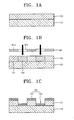
- FIGS. 1A through 1D are schematic cross-sectional views for explaining a method of forming an organic thin film pattern, according to an embodiment of the present invention
- FIGS. 2A through 2D are schematic cross-sectional views for explaining a method of forming an organic semiconductor layer of an organic thin film transistor, according to another embodiment of the present invention.
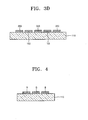
- FIGS. 3A through 3D are schematic cross-sectional views for explaining subsequent processes of forming a unit organic thin film pattern of FIGS. 1A through 1D , according to an embodiment of the present invention
- FIG. 4 illustrates an organic light emitting device including an organic light emitting layer (R, G, and B) of different colors on a substrate, according to an embodiment of the present invention
- FIG. 5 illustrates photos of fine pattern arrays of various organic materials manufactured during a unit organic thin film pattern forming process observed by using an optical microscope, according to an embodiment of the present invention
- FIG. 6 illustrates photos of pixel arrays of organic light emitting materials having different light emitting wavelengths manufactured by continuously performing a unit organic thin film pattern forming process and observed by using a fluorescence microscope, according to an embodiment of the present invention
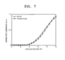
- FIG. 7 is a graph of a comparison of the light emitting characteristics between an organic light emitting device manufactured using the method of the present invention and an organic light emitting device manufactured using the conventional shadow mask technology.
- FIGS. 1A through 1D are schematic cross-sectional views for explaining a method of forming an organic thin film pattern, according to an embodiment of the present invention.
- the method of forming the organic thin film pattern comprises forming a first organic layer 130 on a substrate 110 on which a desired organic thin film pattern is to be formed.
- the substrate 110 may comprise various materials, such as a glass substrate having SiO 2 as a main component, a plastic substrate, or a metal foil, for example.
- a fluorine-based polymer film is formed on the substrate 110 by performing a deep coating method, a spin coating method, etc. on a fluorine-based polymer film.
- the fluorine-based polymer film may be any one of materials represented by Equation 1 through Equation 3 below. Further, the fluorine polymer film may be a functional material containing fluorine in an amount of from about 10 to about 50 %. (where n is an integer between 50 and 1000) (where m is an integer between 50 and 1000, and n is a integer between 50 and 1000) (where n is an integer between 50 and 1000)
- the fluorine-based polymer film is used by melting a fluorinated solvent having a low boiling point, it is possible to form a thin film having a uniform thickness between several tens of nanometers and several micrometers using the deep coating method, and it is useful for adjusting the thickness of a sacrifice layer that will be described later according to a thickness of the desired organic thin film pattern.
- the fluorine-based polymer film 130 is selectively removed by selectively irradiating light energy on the fluorine-based polymer film that is the first organic layer 130, and a sacrifice layer pattern region 131 is formed using the remaining first organic layer 130.
- a laser may be used to irradiate light energy.
- an excimer laser may be used to irradiate light energy.
- a laser ablation process of selectively removing a first part 133 of the first organic layer 130 can be performed by irradiating a laser onto a first mask M1 that is disposed on the first organic layer 130 and has a predetermined pattern.
- the laser that passes through a light transmission portion M1b of the first mask M1 including a light blocking portion M1a and the light transmission portion M1b that are disposed on the first organic layer 130 is absorbed in the part first 133 of the first organic layer 130.
- the part first 133 of the first organic layer 130 that has absorbed the laser is ablated through thermal diffusion.
- a sacrifice layer pattern region 131 of the first organic layer 130 onto which the laser is not irradiated remains as the sacrifice layer pattern 131 that will be described later.
- a mask having a desired predetermined pattern is used to selectively remove a part of the first organic layer 130
- the present embodiments are not limited thereto. That is, although the mask is used to obtain a high resolution pattern, it is possible to directly irradiate the laser onto the first organic layer 130 without a mask.
- a second organic layer 150 is formed on the entire surface of the substrate 110 on which the sacrifice layer 131 is formed.
- the second organic layer 150 may be formed using a deposition process, the present embodiments are not limited thereto and the second organic layer 150 may be formed using various methods of inkjet printing, screen printing, laser induced thermal imaging (LITI), etc.
- the second organic layer 150 includes a layer 153 formed on an upper portion of the substrate 110 on which the sacrifice layer 131 is not formed and a layer 151 formed on the upper portion of the sacrifice layer 131.
- the second organic layer 150 may comprise various materials.
- the second organic layer 150 may comprise an organic light emitting material, an organic color filter material, an organic semiconductor material, etc. This will be described in more detail later.
- a desired pattern 153 of the second organic layer 150 is formed on the substrate 110 using a solvent (not shown).
- a fluorine-based solvent may be used as the solvent.
- HFE-7100 3MTM NOVEC, St. Paul, Minnesota
- Group 17 halogen elements such as fluorine are substantially unresponsive to materials other than halogen elements. Such a chemical property of the fluorine-based solvent does not deteriorate the second organic layer 150 on which a pattern is to be formed.
- the sacrifice layer 131 is removed by using a fluorine-based solvent.
- the second organic layer 151 formed on the sacrifice layer 131 is lifted off.
- the desired part 153 of the second organic layer 151 remains as a pattern on the substrate 110.
- FIGS. 2A through 2D Another embodiment of a method of forming an organic thin film pattern will now be described with reference to FIGS. 2A through 2D .
- FIGS. 2A through 2D are schematic cross-sectional views for explaining a method of forming an organic semiconductor layer of an organic thin film transistor, according to another embodiment of the present invention.
- a first organic layer 230 is formed on a substrate 210 on which a gate electrode 220 and a gate insulation film layer 221 are formed.
- the gate electrode 220 may be formed using a general photolithograph process. For example, a gate metal material is deposited onto the substrate 210, a photoresist (PR) is coated on the deposited substrate 210, and the PR is exposed to light through a photomask (not shown) on which a predetermined pattern is formed.
- the gate electrode 220 is formed using an etching process by soaking the exposed PR in a developing liquid, developing the soaked PR, and forming a desired PR pattern.
- the gate insulation film layer 221 is formed on the gate electrode 220.
- a fluorine-based polymer that is the first organic layer 230 is coated onto the gate insulation layer 221 to a predetermined thickness.
- the fluorine-based polymer film 230 is selectively ablated by selectively irradiating light energy on the fluorine-based polymer film that is the first organic layer 230, and a sacrifice layer pattern 231 is formed using the remaining first organic layer 230.
- a laser may be used to irradiate light energy.
- An excimer laser may be used to irradiate light energy.
- a pulse excimer laser is directly irradiated onto the first organic layer 230 and a part 233 of the first organic layer 230 is directly ablated without using a mask (not shown), and as described above, the part 233 of the first organic layer 230 can be selectively ablated by irradiating a laser onto a mask that is disposed on the first organic layer 230 and has a predetermined pattern.
- the second organic layer 250 is formed on the entire surface of the gate insulation layer 221 on which the sacrifice layer 231 is formed.
- the second organic layer 250 is formed of an organic semiconductor material.
- the organic semiconductor material may include polythiophene and derivatives thereof, poly-p-phenylenevinylene and derivatives thereof, poly-paraphenylene and derivatives thereof, polyprolene and derivatives thereof, polyphenylenevinylene and derivatives thereof, and polythiophene-hetero ring aromatic copolymer and derivatives thereof.
- the organic semiconductor material may include pentacene, tetracene, oligoacene of naphthalene and derivatives thereof, alpha-6-thiophene, oligothiophene of alpha-5-thiophene and derivatives thereof, metal-free or metal containing phthalocyanine and derivatives thereof, pyromellitic dianhydride or pyromellitic diimide and derivatives thereof, perylene tetra carboxylic acid dianhydride or perylene--tetracarboxylic diimide and derivatives thereof.
- the second organic layer 250 may comprise various organic semiconductor materials.
- the second organic layer 250 includes a layer 253 formed on an upper portion of the gate insulation layer 221 on which the sacrifice layer 231 is not formed and a layer 251 formed on the upper portion of the sacrifice layer 231.
- the second organic layer 251 formed on the sacrifice layer 231 is removed by removing the sacrifice layer 231 using a fluorine-based solvent (not shown).
- the desired organic semiconductor layer 253 remains as a pattern on the gate insulation layer 221.
- the organic semiconductor layer 253, which is chemically very sensitive is stably patterned using the fluorine-based solvent that is substantially unresponsive.
- a source electrode 261 and a drain electrode 262 are formed on both sides of the organic semiconductor layer 253 and an organic thin film transistor (OTFT) that is a type of organic semiconductor device is formed.
- OTFT organic thin film transistor
- Photolithography technology that is generally used to manufacture an inorganic semiconductor device is not widely used to manufacture an organic semiconductor device, despite technologies and equipments in which possibilities of a high resolution and a large area process are well established. This is due to a chemical compatibility between a solvent and organic substances used in photolithography technology. An organic substance can be damaged or may deteriorate due to a solvent used to coat or develop a photoresist (PR) during an organic semiconductor device manufacturing process.
- PR photoresist
- the organic thin film does not deteriorate due to the chemical characteristics of a fluorine-based solvent used to form the organic thin film pattern. Further, an additional chemical development process is unnecessary and thus a manufacturing process is very simple. It is possible to form a high resolution organic thin film pattern by using an optical method of removing a sacrifice layer and forming a pattern using laser ablation.
- the organic semiconductor layer of a thin film transistor is formed using the second organic layer formed of an organic semiconductor material in the present embodiment, the present invention is not limited thereto.
- the second organic layer may be used to form an organic light emitting device in which organic light emitting materials of different colors capable of emitting a white light are stacked between an anode and a cathode.
- a sacrifice layer can be formed using a fluorine-based polymer film as a first organic layer on a substrate on which an anode (or a cathode) is formed, the organic light emitting layers of different colors having red, blue, and green colors are sequentially stacked on the entire surface of the sacrifice layer, the sacrifice layer and the organic light emitting layers of different colors formed on the sacrifice layer are removed using a fluorine-based solvent, and the cathode (or the anode) is formed thereon, thereby manufacturing the organic light emitting device capable of emitting the white light.
- FIGS. 3A through 3D Another embodiment of a method of forming an organic thin film pattern will now be described with reference to FIGS. 3A through 3D .
- FIGS. 3A through 3D are schematic cross-sectional views for explaining subsequent processes of forming the unit organic thin film pattern of FIGS. 1A through 1D , according to an embodiment of the present invention.
- a fluorine-based polymer film 330 is coated again on the substrate 110 on which the second organic layer pattern 153 is formed during the first unit organic thin film pattern forming process described with reference to FIGS. 1A through 1D .
- the fluorine-based polymer film 330 is selectively ablated by selectively irradiating light energy onto the fluorine-based polymer film 330, and the remaining fluorine-based polymer film 330 is formed as a second sacrifice layer pattern 331.
- the second sacrifice layer pattern 331 is formed on the second organic layer pattern 153 that has been formed during the first unit organic thin film pattern forming process.
- a light blocking unit M2a is formed on a region on which the second organic layer pattern 153 is formed, and a light transmission unit M2b is formed on a region on which the second organic layer pattern 153 is not formed.
- a fluorine-based polymer film 333 of the region on which the second organic layer pattern 153 is not formed is selectively ablated, and a part of the fluorine-based polymer film 333 of the region on which the second organic layer pattern 153 is formed remains as the second sacrifice layer pattern 331.
- a third organic layer 350 is formed on the entire surface of the substrate 110 on which the second sacrifice layer 331 is formed.
- the third organic layer 350 may be formed using a deposition process, and includes a layer 353 formed on the upper portion of the substrate 110 on which the second sacrifice layer 331 is not formed, and a layer 351 formed on the upper portion of the second sacrifice layer 331.
- the third organic layer 350 may comprise various materials.
- the third organic layer 350 may comprise an organic light emitting material, an organic color filter material, and an organic semiconductor material. This will be described in more detail later.
- a desired pattern 353 of the third organic layer 350 is formed on the substrate 110 using a fluorine-based solvent (not shown).
- the third organic layer pattern 351 formed on the second sacrifice layer 331 is removed by removing the second sacrifice layer 331 using the fluorine-based solvent.
- the second organic layer pattern 153 formed during the first unit organic thin film pattern process and the third organic thin film pattern 353 formed during a present organic thin film pattern forming process remain on the substrate 110.
- the second organic layer pattern 153 and the third organic layer pattern 353 that are different from each other may be formed on the substrate 110 while not deteriorating the second organic layer pattern 153 and the third organic layer pattern 353 due to the chemical property of the fluorine-based solvent.
- the organic light emitting device combines electrons injected into a cathode and holes injected into an anode in an organic layer disposed between the anode and the cathode, excites light emitting molecules of a light emitting layer through the combination of electrons and holes, which then return to a base state, and emits discharged energy as light.
- This is a unit device for realizing an organic light emitting display device.
- the second organic layer pattern 153 and the third organic layer pattern 353 are formed on the anode (or the cathode).
- the organic layer When the organic layer is a low-molecular weight organic substance, the organic layer generally has a multi-layer structure. In the multi-layer structure, at least one, including an emitting layer (EL), of a hole injection layer (HIL), a hole transport layer (HTL), the EL, an electron transport layer (ETL), an electron injection layer (EIL), etc. may be stacked.
- the organic layer may comprise various organic materials, for example, copper phthalocyanine (CuPc), N, N'-di(naphthalene-1-yl)-N, N'-diphenyl-benzidine (NPB), tris(8-hydroxyquinoline) aluminum (Alq3), or the like.
- the HTL may be further included in a direction of the anode from an organic light emitting layer.
- the polymer HTL may comprise polyethylenedioxythiophene (PEDOT) or polyaniline (PANI).
- the polymer organic light-emitting layer may comprise a poly (phenylene vinylene) (PPV), soluble PPV's, Cyano-PPV, polyfluorene, etc.
- One method of forming the organic light emitting display device involves a vacuum process using a shadow mask having a pattern of an organic light emitting layer as a fixed fine pattern.
- a shadow mask having a pattern of an organic light emitting layer as a fixed fine pattern.
- a photolithography technology that is generally used to manufacture an inorganic semiconductor device is not applicable to manufacturing of an organic semiconductor device, despite technologies and equipment in which possibilities of a high resolution and a large area process are well established, since an organic substance can be damaged or deteriorates due to a solvent used to coat or develop a PR during an organic semiconductor device manufacturing process.
- high resolution pattern arrays can be uniformly applied to a wide area compared to the conventional shadow mask technology, and pattern arrays of different organic light emitting materials can be continuously formed by simply repeating a unit process, which is favorable to process simplification and low pricing of the high resolution organic light emitting display.
- the organic thin film does not deteriorate due to the chemical property of a fluorine-based solvent used to form the organic thin film pattern, and an additional chemical developing process is not necessary, thus making a manufacturing process simple.
- two unit organic thin film pattern forming processes are performed to form two different organic thin film patterns, such as a second organic layer pattern and a third organic layer pattern in the present embodiment
- the present embodiments are not limited thereto.
- Three or more unit processes can be repeatedly performed.
- three organic thin film pattern forming processes are performed to manufacture an organic light emitting device including an organic light emitting layer (R, G, and B) of different colors on the substrate as shown in FIG. 4 .
- the method of forming the organic thin film pattern of the present embodiment can be applied to form a pattern of an organic color filter.
- Three organic thin film pattern forming processes are continuously and repeatedly performed to manufacture an organic light emitting device including an organic color filter layer (R, G, and B) of different colors.
- FIG. 5 illustrates photos of fine pattern arrays of various organic materials manufactured during a unit organic thin film pattern forming process observed by using an optical microscope, according to an embodiment.
- a linear pattern having a minimum width of about 10 micrometers can be formed.
- a process resolution can be reduced to several micrometers in terms of an optical method such as laser ablation.
- rectangular pattern arrays of about 100 micrometers in width and about 300 micrometers in height that is similar to a size of a real display pixel are uniformly formed on a wide area.
- the organic thin film patterns can be formed using Alq3, can be formed using other types of organic substances, and can be used using a general pattern process with respect to any organic substance.
- FIG. 6 illustrates photos of pixel arrays of organic light emitting materials having different light emitting wavelengths manufactured by continuously performing a unit organic thin film pattern forming process and observed by using a fluorescence microscope, according to an embodiment.
- fine pixel pattern arrays of 100 ⁇ m X 300 ⁇ m of organic light emitting materials are continuously formed.
- a green organic thin film pattern is formed during a first unit process.
- a blue organic thin film pattern is formed between green organic thin film patterns during a second unit process.
- a lower right portion of the figure shows a cross-sectional structure of the organic thin film patterns.
- the organic thin film patterns have uniform widths, and may have different thicknesses.
- FIG. 7 is a graph of a comparison of the light emitting characteristics between an organic light emitting device manufactured using the method of the present invention and an organic light emitting device manufactured using the conventional shadow mask technology.
- the comparison of light emitting characteristics between the two organic light emitting devices does not show a significant difference.
- a method of the present invention can form a high resolution fine pattern and does not deteriorate device performance compared to the conventional method.
- a method of manufacturing a high resolution organic thin film pattern according to the present embodiment exhibits, for example, the following effects.
- the organic thin film pattern does not deteriorate due to the chemical property of a fluorine-based solution used to form the organic thin film pattern.
- a chemical developing process is not additionally necessary, and thus a manufacturing process is simplified.
- An optical laser ablation method is used to lift off a sacrifice layer and form a pattern, thereby forming the high resolution organic thin film pattern.
- a high resolution pattern array is equally applied to a large area compared to the conventional shadow mask technology, which is favorable to process simplification and low cost of the high resolution organic thin film pattern.
Landscapes
- Engineering & Computer Science (AREA)
- Manufacturing & Machinery (AREA)
- Physics & Mathematics (AREA)
- Optics & Photonics (AREA)
- Electroluminescent Light Sources (AREA)
- Thin Film Transistor (AREA)
- Optical Filters (AREA)
- Exposure And Positioning Against Photoresist Photosensitive Materials (AREA)
Abstract

Description
- The present invention relates to a method of manufacturing an organic thin film pattern, and more particularly, to a method of manufacturing a high resolution organic thin film pattern capable of realizing a simple manufacturing process, stability, and low cost.
- Organic substances are easily combined with other substances and are easily processed so as to exhibit desired electrical optical characteristics and thus they are spotlighted as materials favorable for high performance and low cost next generation electronic devices.
- Although low-molecular organic materials have been used to manufacture organic light emitting display devices or organic thin film transistors using a vacuum deposition method, it is not easy to manufacture high resolution devices due to a vacuum process and limited resolution of a shadow mask. The present invention seeks to overcome the above problems as well as provide additional advantages.
- The present invention also seeks to provide a method of manufacturing a high resolution organic thin film pattern capable of realizing a simple manufacturing process, stability, and low cost.
- According to an aspect of the present invention, there is provided a method of forming an organic thin film pattern, the method including: forming a first organic layer on a substrate; selectively removing the first organic layer by selectively irradiating light energy onto the first organic layer, and forming a remaining part of the first organic layer as a sacrifice layer; forming a second organic layer on the substrate and the entire surface of the sacrifice layer; and lifting off the second organic layer formed on the sacrifice layer by removing the sacrifice layer using a solvent, and forming the remaining second organic layer as a second organic layer pattern.
- In the forming of the first organic layer, the first organic layer may include a fluorine-based polymer.
- In the selective removing of the first organic layer, a laser ablation method may be used to irradiate a laser on a mask having a predetermined pattern disposed on the first organic layer.
- In the selective removing of the first organic layer, an excimer laser may be irradiated.
- In the forming of the second organic layer, the second organic layer may comprise an organic light emitting material of an organic light emitting device (OLED) containing an organic light emitting material disposed on the substrate between a first electrode and a second electrode.
- A plurality of layers of the organic light emitting material of different colors may be formed so as to emit a white light.
- In the forming of the second organic layer, the organic layer may be an active layer of an organic thin film transistor.
- In the forming of the second organic layer, the second organic layer may comprise an organic color filter material.
- In the forming of the second organic layer, the second organic layer may be formed using a deposition method.
- In the lifting off of the second organic layer, the solvent may be a fluorine-based solvent.
- According to another aspect of the present invention, there is provided a method of forming an organic thin film pattern, the method including: (a) forming a first organic layer on a substrate; (b) selectively removing the first organic layer by selectively irradiating light energy onto the first organic layer, and forming a sacrifice layer from a remaining part of the first organic layer; (c) forming a second organic layer on the substrate and the entire surface of the sacrifice layer; (d) lifting off second part of the organic layer formed on the sacrifice layer by removing the sacrifice layer using a solvent, and forming a second organic layer pattern from the remaining second organic layer; and (e) continuously performing a unit process of (a) through (d) on the substrate on which the second organic layer pattern is formed, and forming another second organic layer pattern on a region of the substrate on which the second organic layer pattern is not formed.
- In the forming of the first organic layer, the first organic layer may include a fluorine-based polymer.
- In the selectively removing of the first organic layer, a laser ablation method is used to irradiate laser on a mask having a predetermined pattern disposed on the first organic layer.
- In the selective removing of the first organic layer, an excimer laser may be irradiated.
- In the forming of the second organic layer, the second organic layer may comprise an organic light emitting material of an OLED containing an organic light emitting material disposed on the substrate between a first electrode and a second electrode.
- The organic light emitting material may comprise a low-molecular material.
- In some embodiments, the organic light emitting material formed during the forming of the second organic layer has a different color from the organic light emitting material formed during continuous performing of the unit process.
- The organic light emitting material formed during the forming of the second organic layer and the organic light emitting material formed during continuous performing of the unit process may realize full colors.
- In the forming of the second organic layer, the second organic layer may comprise a color filter material.
- The color filter material formed during the forming of the second organic layer may have a different color from the color filter materials formed during continuous performing of the unit process.
- The color filter material formed during the forming of the second organic layer and the color filter material formed during continuous performing of the unit process may realize full colors.
- In the forming of the second organic layer, the second organic layer may be formed using a deposition method.
- In the lifting off of the second organic layer, the solvent may be a fluorine-based solvent. Also, step (e) above may be repeatedly performed a predetermined number of times.
- At least some of the above and other features of the invention are set out in the claims.
- The above and other features and advantages of the present invention will become more apparent from the following description of embodiments thereof which is made with reference to the attached drawings in which:
-
FIGS. 1A through 1D are schematic cross-sectional views for explaining a method of forming an organic thin film pattern, according to an embodiment of the present invention; -
FIGS. 2A through 2D are schematic cross-sectional views for explaining a method of forming an organic semiconductor layer of an organic thin film transistor, according to another embodiment of the present invention; -
FIGS. 3A through 3D are schematic cross-sectional views for explaining subsequent processes of forming a unit organic thin film pattern ofFIGS. 1A through 1D , according to an embodiment of the present invention; -
FIG. 4 illustrates an organic light emitting device including an organic light emitting layer (R, G, and B) of different colors on a substrate, according to an embodiment of the present invention; -
FIG. 5 illustrates photos of fine pattern arrays of various organic materials manufactured during a unit organic thin film pattern forming process observed by using an optical microscope, according to an embodiment of the present invention; -
FIG. 6 illustrates photos of pixel arrays of organic light emitting materials having different light emitting wavelengths manufactured by continuously performing a unit organic thin film pattern forming process and observed by using a fluorescence microscope, according to an embodiment of the present invention; and -
FIG. 7 is a graph of a comparison of the light emitting characteristics between an organic light emitting device manufactured using the method of the present invention and an organic light emitting device manufactured using the conventional shadow mask technology. - Hereinafter, embodiments according to the present invention will be described in detail with reference to the accompanying drawings.
-
FIGS. 1A through 1D are schematic cross-sectional views for explaining a method of forming an organic thin film pattern, according to an embodiment of the present invention. Referring toFIG. 1A , the method of forming the organic thin film pattern comprises forming a firstorganic layer 130 on asubstrate 110 on which a desired organic thin film pattern is to be formed. - The
substrate 110 may comprise various materials, such as a glass substrate having SiO2 as a main component, a plastic substrate, or a metal foil, for example. - A fluorine-based polymer film is formed on the
substrate 110 by performing a deep coating method, a spin coating method, etc. on a fluorine-based polymer film. The fluorine-based polymer film may be any one of materials represented by Equation 1 through Equation 3 below. Further, the fluorine polymer film may be a functional material containing fluorine in an amount of from about 10 to about 50 %.


- If the fluorine-based polymer film is used by melting a fluorinated solvent having a low boiling point, it is possible to form a thin film having a uniform thickness between several tens of nanometers and several micrometers using the deep coating method, and it is useful for adjusting the thickness of a sacrifice layer that will be described later according to a thickness of the desired organic thin film pattern.
- Referring to
FIG. 1B , the fluorine-basedpolymer film 130 is selectively removed by selectively irradiating light energy on the fluorine-based polymer film that is the firstorganic layer 130, and a sacrificelayer pattern region 131 is formed using the remaining firstorganic layer 130. - In this regard, a laser may be used to irradiate light energy. For example, an excimer laser may be used to irradiate light energy. Further, a laser ablation process of selectively removing a
first part 133 of the firstorganic layer 130 can be performed by irradiating a laser onto a first mask M1 that is disposed on the firstorganic layer 130 and has a predetermined pattern. - The laser that passes through a light transmission portion M1b of the first mask M1 including a light blocking portion M1a and the light transmission portion M1b that are disposed on the first
organic layer 130 is absorbed in the part first 133 of the firstorganic layer 130. The part first 133 of the firstorganic layer 130 that has absorbed the laser is ablated through thermal diffusion. A sacrificelayer pattern region 131 of the firstorganic layer 130 onto which the laser is not irradiated remains as thesacrifice layer pattern 131 that will be described later. - Although a mask having a desired predetermined pattern is used to selectively remove a part of the first
organic layer 130, the present embodiments are not limited thereto. That is, although the mask is used to obtain a high resolution pattern, it is possible to directly irradiate the laser onto the firstorganic layer 130 without a mask. - Referring to
FIG. 1C , a secondorganic layer 150 is formed on the entire surface of thesubstrate 110 on which thesacrifice layer 131 is formed. - Although the second
organic layer 150 may be formed using a deposition process, the present embodiments are not limited thereto and the secondorganic layer 150 may be formed using various methods of inkjet printing, screen printing, laser induced thermal imaging (LITI), etc. The secondorganic layer 150 includes alayer 153 formed on an upper portion of thesubstrate 110 on which thesacrifice layer 131 is not formed and alayer 151 formed on the upper portion of thesacrifice layer 131. - As described above, the second
organic layer 150 may comprise various materials. For example, the secondorganic layer 150 may comprise an organic light emitting material, an organic color filter material, an organic semiconductor material, etc. This will be described in more detail later. - Referring to
FIG. 1D , a desiredpattern 153 of the secondorganic layer 150 is formed on thesubstrate 110 using a solvent (not shown). - If a fluorine-based polymer film is used as the first
organic layer 130, a fluorine-based solvent may be used as the solvent. In the present embodiment, HFE-7100 (3M™ NOVEC, St. Paul, Minnesota) is used as the fluorine-based solvent. Group 17 halogen elements such as fluorine are substantially unresponsive to materials other than halogen elements. Such a chemical property of the fluorine-based solvent does not deteriorate the secondorganic layer 150 on which a pattern is to be formed. - The
sacrifice layer 131 is removed by using a fluorine-based solvent. The secondorganic layer 151 formed on thesacrifice layer 131 is lifted off. Thus, the desiredpart 153 of the secondorganic layer 151 remains as a pattern on thesubstrate 110. - Another embodiment of a method of forming an organic thin film pattern will now be described with reference to
FIGS. 2A through 2D . -
FIGS. 2A through 2D are schematic cross-sectional views for explaining a method of forming an organic semiconductor layer of an organic thin film transistor, according to another embodiment of the present invention. - Referring to
FIG. 2A , a firstorganic layer 230 is formed on asubstrate 210 on which agate electrode 220 and a gateinsulation film layer 221 are formed. - The
gate electrode 220 may be formed using a general photolithograph process. For example, a gate metal material is deposited onto thesubstrate 210, a photoresist (PR) is coated on the depositedsubstrate 210, and the PR is exposed to light through a photomask (not shown) on which a predetermined pattern is formed. Thegate electrode 220 is formed using an etching process by soaking the exposed PR in a developing liquid, developing the soaked PR, and forming a desired PR pattern. The gateinsulation film layer 221 is formed on thegate electrode 220. A fluorine-based polymer that is the firstorganic layer 230 is coated onto thegate insulation layer 221 to a predetermined thickness. - Referring to
FIG. 2B , the fluorine-basedpolymer film 230 is selectively ablated by selectively irradiating light energy on the fluorine-based polymer film that is the firstorganic layer 230, and asacrifice layer pattern 231 is formed using the remaining firstorganic layer 230. In this regard, as mentioned above, a laser may be used to irradiate light energy. An excimer laser may be used to irradiate light energy. - A pulse excimer laser is directly irradiated onto the first
organic layer 230 and apart 233 of the firstorganic layer 230 is directly ablated without using a mask (not shown), and as described above, thepart 233 of the firstorganic layer 230 can be selectively ablated by irradiating a laser onto a mask that is disposed on the firstorganic layer 230 and has a predetermined pattern. - Referring to
FIG. 2C , the secondorganic layer 250 is formed on the entire surface of thegate insulation layer 221 on which thesacrifice layer 231 is formed. - The second
organic layer 250 is formed of an organic semiconductor material. When the secondorganic layer 250 is formed of a polymer organic material, the organic semiconductor material may include polythiophene and derivatives thereof, poly-p-phenylenevinylene and derivatives thereof, poly-paraphenylene and derivatives thereof, polyprolene and derivatives thereof, polyphenylenevinylene and derivatives thereof, and polythiophene-hetero ring aromatic copolymer and derivatives thereof. When the secondorganic layer 250 is formed of a low-molecular organic material, the organic semiconductor material may include pentacene, tetracene, oligoacene of naphthalene and derivatives thereof, alpha-6-thiophene, oligothiophene of alpha-5-thiophene and derivatives thereof, metal-free or metal containing phthalocyanine and derivatives thereof, pyromellitic dianhydride or pyromellitic diimide and derivatives thereof, perylene tetra carboxylic acid dianhydride or perylene--tetracarboxylic diimide and derivatives thereof. In addition, the secondorganic layer 250 may comprise various organic semiconductor materials. - The second
organic layer 250 includes alayer 253 formed on an upper portion of thegate insulation layer 221 on which thesacrifice layer 231 is not formed and alayer 251 formed on the upper portion of thesacrifice layer 231. - Referring to
FIG. 2D , the secondorganic layer 251 formed on thesacrifice layer 231 is removed by removing thesacrifice layer 231 using a fluorine-based solvent (not shown). Thus, the desiredorganic semiconductor layer 253 remains as a pattern on thegate insulation layer 221. In this regard, as described above, theorganic semiconductor layer 253, which is chemically very sensitive, is stably patterned using the fluorine-based solvent that is substantially unresponsive. Asource electrode 261 and adrain electrode 262 are formed on both sides of theorganic semiconductor layer 253 and an organic thin film transistor (OTFT) that is a type of organic semiconductor device is formed. - Photolithography technology that is generally used to manufacture an inorganic semiconductor device is not widely used to manufacture an organic semiconductor device, despite technologies and equipments in which possibilities of a high resolution and a large area process are well established. This is due to a chemical compatibility between a solvent and organic substances used in photolithography technology. An organic substance can be damaged or may deteriorate due to a solvent used to coat or develop a photoresist (PR) during an organic semiconductor device manufacturing process.
- However, according to the method of forming the organic thin film pattern of the organic semiconductor device of the present embodiment, the organic thin film does not deteriorate due to the chemical characteristics of a fluorine-based solvent used to form the organic thin film pattern. Further, an additional chemical development process is unnecessary and thus a manufacturing process is very simple. It is possible to form a high resolution organic thin film pattern by using an optical method of removing a sacrifice layer and forming a pattern using laser ablation.
- Although a typical bottom gate thin film transistor in which the
gate electrode 220 is disposed under theorganic semiconductor layer 253, and the source and drainelectrodes organic semiconductor layer 253 is described in the present embodiment, this is just illustrative and various structures of organic thin film transistors may be applied. - Although the organic semiconductor layer of a thin film transistor is formed using the second organic layer formed of an organic semiconductor material in the present embodiment, the present invention is not limited thereto. For example, the second organic layer may be used to form an organic light emitting device in which organic light emitting materials of different colors capable of emitting a white light are stacked between an anode and a cathode. For example, a sacrifice layer can be formed using a fluorine-based polymer film as a first organic layer on a substrate on which an anode (or a cathode) is formed, the organic light emitting layers of different colors having red, blue, and green colors are sequentially stacked on the entire surface of the sacrifice layer, the sacrifice layer and the organic light emitting layers of different colors formed on the sacrifice layer are removed using a fluorine-based solvent, and the cathode (or the anode) is formed thereon, thereby manufacturing the organic light emitting device capable of emitting the white light.
- Another embodiment of a method of forming an organic thin film pattern will now be described with reference to
FIGS. 3A through 3D . -
FIGS. 3A through 3D are schematic cross-sectional views for explaining subsequent processes of forming the unit organic thin film pattern ofFIGS. 1A through 1D , according to an embodiment of the present invention. - Referring to
FIG. 3A , a fluorine-basedpolymer film 330 is coated again on thesubstrate 110 on which the secondorganic layer pattern 153 is formed during the first unit organic thin film pattern forming process described with reference toFIGS. 1A through 1D . - Referring to
FIG. 3B , the fluorine-basedpolymer film 330 is selectively ablated by selectively irradiating light energy onto the fluorine-basedpolymer film 330, and the remaining fluorine-basedpolymer film 330 is formed as a secondsacrifice layer pattern 331. In this regard, the secondsacrifice layer pattern 331 is formed on the secondorganic layer pattern 153 that has been formed during the first unit organic thin film pattern forming process. - When a second mask M2 is used to form the second
sacrifice layer pattern 331, a light blocking unit M2a is formed on a region on which the secondorganic layer pattern 153 is formed, and a light transmission unit M2b is formed on a region on which the secondorganic layer pattern 153 is not formed. By irradiating a laser onto the second mask M2, a fluorine-basedpolymer film 333 of the region on which the secondorganic layer pattern 153 is not formed is selectively ablated, and a part of the fluorine-basedpolymer film 333 of the region on which the secondorganic layer pattern 153 is formed remains as the secondsacrifice layer pattern 331. - Referring to
FIG. 3C , a thirdorganic layer 350 is formed on the entire surface of thesubstrate 110 on which thesecond sacrifice layer 331 is formed. The thirdorganic layer 350 may be formed using a deposition process, and includes alayer 353 formed on the upper portion of thesubstrate 110 on which thesecond sacrifice layer 331 is not formed, and alayer 351 formed on the upper portion of thesecond sacrifice layer 331. - As described above, the third
organic layer 350 may comprise various materials. For example, the thirdorganic layer 350 may comprise an organic light emitting material, an organic color filter material, and an organic semiconductor material. This will be described in more detail later. - Referring to
FIG. 3D , a desiredpattern 353 of the thirdorganic layer 350 is formed on thesubstrate 110 using a fluorine-based solvent (not shown). - The third
organic layer pattern 351 formed on thesecond sacrifice layer 331 is removed by removing thesecond sacrifice layer 331 using the fluorine-based solvent. Thus, the secondorganic layer pattern 153 formed during the first unit organic thin film pattern process and the third organicthin film pattern 353 formed during a present organic thin film pattern forming process (hereinafter, referred to as "a second unit organic thin film pattern forming process") remain on thesubstrate 110. - Therefore, the second
organic layer pattern 153 and the thirdorganic layer pattern 353 that are different from each other may be formed on thesubstrate 110 while not deteriorating the secondorganic layer pattern 153 and the thirdorganic layer pattern 353 due to the chemical property of the fluorine-based solvent. - Hereinafter, an example of using the second
organic layer pattern 153 and the thirdorganic layer pattern 353 as organic layers of an organic light emitting device will be described. - The organic light emitting device combines electrons injected into a cathode and holes injected into an anode in an organic layer disposed between the anode and the cathode, excites light emitting molecules of a light emitting layer through the combination of electrons and holes, which then return to a base state, and emits discharged energy as light. This is a unit device for realizing an organic light emitting display device. Although not shown, the second
organic layer pattern 153 and the thirdorganic layer pattern 353 are formed on the anode (or the cathode). - When the organic layer is a low-molecular weight organic substance, the organic layer generally has a multi-layer structure. In the multi-layer structure, at least one, including an emitting layer (EL), of a hole injection layer (HIL), a hole transport layer (HTL), the EL, an electron transport layer (ETL), an electron injection layer (EIL), etc. may be stacked. The organic layer may comprise various organic materials, for example, copper phthalocyanine (CuPc), N, N'-di(naphthalene-1-yl)-N, N'-diphenyl-benzidine (NPB), tris(8-hydroxyquinoline) aluminum (Alq3), or the like. When the organic layer is a polymer organic substance, the HTL may be further included in a direction of the anode from an organic light emitting layer. The polymer HTL may comprise polyethylenedioxythiophene (PEDOT) or polyaniline (PANI). The polymer organic light-emitting layer may comprise a poly (phenylene vinylene) (PPV), soluble PPV's, Cyano-PPV, polyfluorene, etc.
- One method of forming the organic light emitting display device involves a vacuum process using a shadow mask having a pattern of an organic light emitting layer as a fixed fine pattern. However, there are many problems in manufacturing a large-sized display device due to limitations of the vacuum process and resolution of the shadow mask.
- Further, a photolithography technology that is generally used to manufacture an inorganic semiconductor device is not applicable to manufacturing of an organic semiconductor device, despite technologies and equipment in which possibilities of a high resolution and a large area process are well established, since an organic substance can be damaged or deteriorates due to a solvent used to coat or develop a PR during an organic semiconductor device manufacturing process.
- Further, to solve the above problems, although (Laser Induced Thermal Imaging) LITI technology of transferring a previously formed organic thin film onto a substrate by using a laser has been developed, since the laser is directly irradiated onto the organic thin film, the material characteristics of the organic thin film or operating characteristics of a device may be adversely affected.
- However, according to the method of forming the organic thin film pattern of the organic light emitting device of the present embodiment, high resolution pattern arrays can be uniformly applied to a wide area compared to the conventional shadow mask technology, and pattern arrays of different organic light emitting materials can be continuously formed by simply repeating a unit process, which is favorable to process simplification and low pricing of the high resolution organic light emitting display.
- The organic thin film does not deteriorate due to the chemical property of a fluorine-based solvent used to form the organic thin film pattern, and an additional chemical developing process is not necessary, thus making a manufacturing process simple.
- It is possible to form a high resolution organic thin film pattern by using an optical method of ablating a sacrifice layer and forming a pattern by using laser ablation.
- Although two unit organic thin film pattern forming processes are performed to form two different organic thin film patterns, such as a second organic layer pattern and a third organic layer pattern in the present embodiment, the present embodiments are not limited thereto. Three or more unit processes can be repeatedly performed. For example, three organic thin film pattern forming processes are performed to manufacture an organic light emitting device including an organic light emitting layer (R, G, and B) of different colors on the substrate as shown in
FIG. 4 . - Further, the method of forming the organic thin film pattern of the present embodiment can be applied to form a pattern of an organic color filter. Three organic thin film pattern forming processes are continuously and repeatedly performed to manufacture an organic light emitting device including an organic color filter layer (R, G, and B) of different colors.
-
FIG. 5 illustrates photos of fine pattern arrays of various organic materials manufactured during a unit organic thin film pattern forming process observed by using an optical microscope, according to an embodiment. - Referring to
FIG. 5 , a linear pattern having a minimum width of about 10 micrometers can be formed. A process resolution can be reduced to several micrometers in terms of an optical method such as laser ablation. Further, rectangular pattern arrays of about 100 micrometers in width and about 300 micrometers in height that is similar to a size of a real display pixel are uniformly formed on a wide area. The organic thin film patterns can be formed using Alq3, can be formed using other types of organic substances, and can be used using a general pattern process with respect to any organic substance. -
FIG. 6 illustrates photos of pixel arrays of organic light emitting materials having different light emitting wavelengths manufactured by continuously performing a unit organic thin film pattern forming process and observed by using a fluorescence microscope, according to an embodiment. - Referring to
FIG. 6 , fine pixel pattern arrays of 100 µm X 300 µm of organic light emitting materials are continuously formed. In a left photo, a green organic thin film pattern is formed during a first unit process. In a right photo, a blue organic thin film pattern is formed between green organic thin film patterns during a second unit process. - A lower right portion of the figure shows a cross-sectional structure of the organic thin film patterns. The organic thin film patterns have uniform widths, and may have different thicknesses.
-
FIG. 7 is a graph of a comparison of the light emitting characteristics between an organic light emitting device manufactured using the method of the present invention and an organic light emitting device manufactured using the conventional shadow mask technology. - Referring to
FIG. 7 , the comparison of light emitting characteristics between the two organic light emitting devices does not show a significant difference. As described above, a method of the present invention can form a high resolution fine pattern and does not deteriorate device performance compared to the conventional method. - A method of manufacturing a high resolution organic thin film pattern according to the present embodiment exhibits, for example, the following effects.
- The organic thin film pattern does not deteriorate due to the chemical property of a fluorine-based solution used to form the organic thin film pattern.
- A chemical developing process is not additionally necessary, and thus a manufacturing process is simplified.
- An optical laser ablation method is used to lift off a sacrifice layer and form a pattern, thereby forming the high resolution organic thin film pattern.
- When an organic light emitting layer of an organic light emitting display device is formed, a high resolution pattern array is equally applied to a large area compared to the conventional shadow mask technology, which is favorable to process simplification and low cost of the high resolution organic thin film pattern.
Claims (18)
- A method of forming an organic thin film pattern, the method comprising:(a) forming a first organic layer on a substrate;(b) selectively removing a part of the first organic layer by selectively irradiating light energy onto the first organic layer, and leaving a remaining part of the first organic layer as a sacrifice layer;(c) forming a second organic layer on the substrate and the entire surface of the sacrifice layer; and(d) lifting off the second organic layer formed on the sacrifice layer by removing the sacrifice layer using a solvent, and leaving the remaining second organic layer as a second organic layer pattern.
- A method according to claim 1, wherein the first organic layer comprises a fluorine-based polymer.
- A method according to claim 1 or 2, wherein, in the selective removing of the first organic layer, a laser ablation method is used to irradiate a laser on a mask having a predetermined pattern disposed on the first organic layer.
- A method according to claim 3, wherein, in the selective removing of the first organic layer, an excimer laser is irradiated.
- A method according to any preceding claim, wherein the second organic layer is formed of an organic light emitting material of an organic light emitting device (OLED) in which the organic light emitting material is disposed on the substrate between a first electrode and a second electrode.
- A method according claim 5, wherein a plurality of layers of the organic light emitting material are formed, and the plurality of layers emit respectively different colors of light so as to collectively emit a white light.
- A method according to one of claims 1 to 4, wherein the second organic layer, the organic layer is an active layer of an organic thin film transistor.
- A method according to one of claims 1 to 4, wherein, in the forming of the second organic layer, the second organic layer is formed of an organic color filter material.
- A method according to any preceding claim, wherein, in the forming of the second organic layer, the second organic layer is formed using a deposition method.
- A method according to any preceding claim, wherein, in the lifting off of the second organic layer, the solvent is a fluorine-based solvent.
- A method of forming an organic thin film pattern according to any preceding claim, the method comprising:repeatedly performing the steps of (a) to (d) on the substrate on which the second organic layer pattern is formed, and forming another second organic layer pattern on a region of the substrate on which the second organic layer pattern is not formed.
- A method according to claim 11, wherein, in the forming of the first organic layer, the first organic layer comprises a fluorine-based polymer.
- A method according to claim 11 when dependent upon claim 5, wherein the second organic light emitting material formed during the forming of the second organic layer is adapted to emit light a different color from the organic light emitting material formed during each performance of steps (a) to (d).
- A method according to claim 13, wherein the organic light emitting material formed during the forming of the second organic layer and the organic light emitting material formed during repeated performing of steps (a) to (d) emits full colors.
- A method according to claim 11 when dependent upon claim 6, wherein the color filter material formed during the forming of the second organic layer has an overall different color from the color filter materials formed during each performance of steps (a) to (d).
- A method according to claim 15, wherein the color filter material formed during the forming of the second organic layer and the color filter material formed during repeated performing of steps (a) to (d) realize full colors.
- A method according to one of claims 11 to 16, wherein step (e) is repeatedly performed a predetermined number of times.
- A method according to any preceding claim, wherein the organic light emitting material comprises a low-molecular weight material.
Applications Claiming Priority (1)
| Application Number | Priority Date | Filing Date | Title |
|---|---|---|---|
| KR1020100002377A KR101108162B1 (en) | 2010-01-11 | 2010-01-11 | High resolution organic thin film pattern formation method |
Publications (3)
| Publication Number | Publication Date |
|---|---|
| EP2343749A2 true EP2343749A2 (en) | 2011-07-13 |
| EP2343749A3 EP2343749A3 (en) | 2014-04-02 |
| EP2343749B1 EP2343749B1 (en) | 2016-07-13 |
Family
ID=43742449
Family Applications (1)
| Application Number | Title | Priority Date | Filing Date |
|---|---|---|---|
| EP11250012.9A Active EP2343749B1 (en) | 2010-01-11 | 2011-01-07 | Method of manufacturing high resolution organic thin film pattern |
Country Status (6)
| Country | Link |
|---|---|
| US (1) | US8778600B2 (en) |
| EP (1) | EP2343749B1 (en) |
| JP (1) | JP5548590B2 (en) |
| KR (1) | KR101108162B1 (en) |
| CN (2) | CN102169959A (en) |
| TW (1) | TWI472079B (en) |
Cited By (1)
| Publication number | Priority date | Publication date | Assignee | Title |
|---|---|---|---|---|
| WO2015144930A1 (en) * | 2014-03-28 | 2015-10-01 | Imec Vzw | High-resolution patterning of multiple layers side by side |
Families Citing this family (31)
| Publication number | Priority date | Publication date | Assignee | Title |
|---|---|---|---|---|
| JPH07121408B2 (en) | 1986-12-26 | 1995-12-25 | 昭和アルミニウム株式会社 | Method and device for manufacturing metal extruded material coated with dissimilar metals |
| KR101698462B1 (en) | 2011-02-07 | 2017-01-20 | 어플라이드 머티어리얼스, 인코포레이티드 | Method for encapsulating an organic light emitting diode |
| EP2579313B1 (en) * | 2011-09-22 | 2021-10-27 | LG Display Co., Ltd. | Organic light emitting diode display device and method of fabricating the same |
| US9449809B2 (en) | 2012-07-20 | 2016-09-20 | Applied Materials, Inc. | Interface adhesion improvement method |
| KR101901330B1 (en) * | 2012-09-19 | 2018-09-27 | 삼성디스플레이 주식회사 | Method of manufacturing organic electroluminescent display |
| KR101976829B1 (en) * | 2012-12-21 | 2019-05-13 | 엘지디스플레이 주식회사 | Large Area Organic Light Emitting Diode Display And Method For Manufacturing The Same |
| KR102122518B1 (en) * | 2012-12-21 | 2020-06-15 | 엘지디스플레이 주식회사 | Transparent Organic Light Emitting Diode Display Having Hight Transmittance And Method For Manufacturing The Same |
| US10020448B2 (en) * | 2013-09-19 | 2018-07-10 | Joled Inc. | Method for manufacturing organic light-emitting device and method of manufacturing display unit |
| KR102177169B1 (en) * | 2013-12-02 | 2020-11-10 | 엘지디스플레이 주식회사 | Method of fabricating flexible organic light emitting diode display device |
| CN103887157B (en) * | 2014-03-12 | 2021-08-27 | 京东方科技集团股份有限公司 | Optical mask plate and laser stripping device |
| KR20170039306A (en) * | 2014-08-14 | 2017-04-10 | 광주과학기술원 | Orthogonal patterning method |
| CN104319293A (en) * | 2014-11-10 | 2015-01-28 | 京东方科技集团股份有限公司 | Metallic oxide thin film transistor, array substrate, manufacturing method and display device |
| KR102318418B1 (en) | 2014-12-08 | 2021-10-28 | 삼성디스플레이 주식회사 | Organic light emitting display device and manufacturing method thereof |
| KR102354973B1 (en) | 2015-06-10 | 2022-01-25 | 삼성디스플레이 주식회사 | Flexible display apparatus and manufacturing method thereof |
| KR102360093B1 (en) | 2015-07-22 | 2022-02-09 | 삼성디스플레이 주식회사 | Organic light-emitting display apparatus and the method for manufacturing of the organic light-emitting display apparatus |
| KR102465384B1 (en) * | 2015-07-23 | 2022-11-10 | 삼성디스플레이 주식회사 | display apparatus |
| KR102313365B1 (en) * | 2015-08-25 | 2021-10-18 | 삼성디스플레이 주식회사 | Method for manufacturing of organic light-emitting display apparatus |
| CN105575817A (en) * | 2015-12-17 | 2016-05-11 | 武汉华星光电技术有限公司 | Manufacturing method of film transistor |
| US10243175B2 (en) * | 2016-02-02 | 2019-03-26 | Samsung Display Co., Ltd. | Organic light-emitting apparatus fabricated using a fluoropolymer and method of manufacturing the same |
| CN106004074B (en) * | 2016-05-24 | 2017-08-29 | 山东华菱电子股份有限公司 | A kind of manufacture method of thermal printing head heating base plate |
| KR20180046257A (en) * | 2016-10-27 | 2018-05-08 | 삼성전자주식회사 | Method of manufacturing thin film transistor, thin film transistor, and electronic device comprising the thin film transistor |
| CN106450028A (en) * | 2016-10-31 | 2017-02-22 | 武汉华星光电技术有限公司 | A color film substrate and a manufacturing method thereof |
| US10756235B2 (en) | 2017-03-09 | 2020-08-25 | Enkris Semiconductor, Inc | Stripped method for preparing semiconductor structure |
| KR102606282B1 (en) | 2017-06-19 | 2023-11-27 | 삼성디스플레이 주식회사 | Display device |
| CN107732031A (en) * | 2017-09-29 | 2018-02-23 | 京东方科技集团股份有限公司 | The preparation method and organic electroluminescence display panel of organic electroluminescence display panel |
| CN109065761B (en) * | 2018-07-26 | 2020-07-10 | 武汉华星光电半导体显示技术有限公司 | O L ED substrate and manufacturing method thereof |
| CN109148364A (en) * | 2018-08-29 | 2019-01-04 | 深圳华信嘉源科技有限公司 | A kind of manufacture craft of high resolution matrix screen |
| CN110346960A (en) * | 2019-07-02 | 2019-10-18 | 深圳市华星光电技术有限公司 | A kind of preparation method and applications of black matrix" on glass substrate |
| WO2021184256A1 (en) * | 2020-03-18 | 2021-09-23 | 京东方科技集团股份有限公司 | Quantum dot light emitting device and manufacturing method therefor, and manufacturing method for quantum dot display panel |
| JP7825143B2 (en) * | 2020-06-03 | 2026-03-06 | 大日本印刷株式会社 | Electronic device, method for manufacturing electronic device, and deposition mask group |
| CN114373878B (en) * | 2020-10-14 | 2023-10-20 | 北京京东方技术开发有限公司 | Method for producing patterned quantum dot light-emitting layer, method for producing light-emitting device |
Family Cites Families (26)
| Publication number | Priority date | Publication date | Assignee | Title |
|---|---|---|---|---|
| JP3083178B2 (en) * | 1991-07-17 | 2000-09-04 | 三井化学株式会社 | Laser Ablation Microfabrication Using Intermediate Absorption |
| JP3212405B2 (en) * | 1992-07-20 | 2001-09-25 | 富士通株式会社 | Excimer laser processing method and apparatus |
| JPH0778820A (en) * | 1993-09-08 | 1995-03-20 | Fujitsu Ltd | Method of forming thin film pattern |
| JP3874989B2 (en) * | 2000-03-21 | 2007-01-31 | シャープ株式会社 | Pattern formation method |
| JP2002047560A (en) * | 2000-07-31 | 2002-02-15 | Victor Co Of Japan Ltd | Vacuum evaporation mask, method of forming thin film pattern using the same, and method of manufacturing EL element |
| JP2002170669A (en) * | 2000-12-01 | 2002-06-14 | Tdk Corp | Organic EL display device and manufacturing method thereof |
| DE10135640A1 (en) * | 2001-07-21 | 2003-02-06 | Covion Organic Semiconductors | Organic semiconductor solution used for organic integrated switches, organic field effect transistors, organic thin film transistors, organic solar cells and organic laser diodes contains one or more additives |
| GB0207134D0 (en) * | 2002-03-27 | 2002-05-08 | Cambridge Display Tech Ltd | Method of preparation of organic optoelectronic and electronic devices and devices thereby obtained |
| US6821799B2 (en) * | 2002-06-13 | 2004-11-23 | University Of Cincinnati | Method of fabricating a multi-color light emissive display |
| EP1529317A2 (en) * | 2002-08-06 | 2005-05-11 | Avecia Limited | Organic electronic devices |
| SG129274A1 (en) * | 2003-02-19 | 2007-02-26 | Mitsubishi Gas Chemical Co | Cleaaning solution and cleaning process using the solution |
| JP4586334B2 (en) * | 2003-05-07 | 2010-11-24 | ソニー株式会社 | Field effect transistor and manufacturing method thereof |
| JPWO2005045911A1 (en) * | 2003-11-11 | 2007-11-29 | 旭硝子株式会社 | Pattern forming method, electronic circuit manufactured thereby, and electronic apparatus using the same |
| JP2005183782A (en) * | 2003-12-22 | 2005-07-07 | Sony Corp | Pattern formation method based on lift-off method |
| KR20050077525A (en) * | 2004-01-27 | 2005-08-03 | 삼성전자주식회사 | Method of forming organic semiconductor pattern and method of manufacturing organic thin film transistor using the same |
| KR100685803B1 (en) * | 2004-12-14 | 2007-02-22 | 삼성에스디아이 주식회사 | Method for manufacturing organic electroluminescent device |
| KR100833017B1 (en) | 2005-05-12 | 2008-05-27 | 주식회사 엘지화학 | Method for preparing a high resolution pattern with direct writing means |
| KR101209046B1 (en) * | 2005-07-27 | 2012-12-06 | 삼성디스플레이 주식회사 | Thin film transistor substrate and method of making thin film transistor substrate |
| KR20070019495A (en) * | 2005-08-12 | 2007-02-15 | 삼성에스디아이 주식회사 | White organic light emitting device and its manufacturing method |
| JP4293467B2 (en) | 2006-09-28 | 2009-07-08 | 国立大学法人京都大学 | Manufacturing method of organic material device |
| US8420978B2 (en) * | 2007-01-18 | 2013-04-16 | The Board Of Trustees Of The University Of Illinois | High throughput, low cost dual-mode patterning method for large area substrates |
| JP5144127B2 (en) * | 2007-05-23 | 2013-02-13 | キヤノン株式会社 | Method for producing mold for nanoimprint |
| KR100971066B1 (en) | 2007-06-29 | 2010-07-20 | 샌트랄 글래스 컴퍼니 리미티드 | Fluorine-containing compound, fluorine-containing polymer compound, negative type resist composition and pattern formation method using the same |
| US20090091255A1 (en) * | 2007-10-09 | 2009-04-09 | Sung-Hoon Lee | White organic light emitting device |
| DE102007057650A1 (en) | 2007-11-28 | 2009-06-04 | H.C. Starck Gmbh | Structuring of conductive polymer layers by means of the lift-off process |
| CN102037409B (en) | 2008-05-23 | 2013-12-11 | 康奈尔大学 | Orthogonal processing of organic materials used in electronic and electrical devices |
-
2010
- 2010-01-11 KR KR1020100002377A patent/KR101108162B1/en active Active
- 2010-11-08 JP JP2010249571A patent/JP5548590B2/en active Active
- 2010-12-27 US US12/979,260 patent/US8778600B2/en active Active
-
2011
- 2011-01-05 CN CN2011100065445A patent/CN102169959A/en active Pending
- 2011-01-05 CN CN201610115813.4A patent/CN105742495B/en active Active
- 2011-01-07 EP EP11250012.9A patent/EP2343749B1/en active Active
- 2011-01-11 TW TW100101020A patent/TWI472079B/en active
Non-Patent Citations (1)
| Title |
|---|
| None |
Cited By (2)
| Publication number | Priority date | Publication date | Assignee | Title |
|---|---|---|---|---|
| WO2015144930A1 (en) * | 2014-03-28 | 2015-10-01 | Imec Vzw | High-resolution patterning of multiple layers side by side |
| KR20160138966A (en) * | 2014-03-28 | 2016-12-06 | 아이엠이씨 브이제트더블유 | High-resolution patterning of multiple layers side by side |
Also Published As
| Publication number | Publication date |
|---|---|
| KR20110082415A (en) | 2011-07-19 |
| EP2343749B1 (en) | 2016-07-13 |
| JP5548590B2 (en) | 2014-07-16 |
| KR101108162B1 (en) | 2012-01-31 |
| US8778600B2 (en) | 2014-07-15 |
| CN105742495B (en) | 2020-06-05 |
| CN102169959A (en) | 2011-08-31 |
| US20110171584A1 (en) | 2011-07-14 |
| JP2011141526A (en) | 2011-07-21 |
| CN105742495A (en) | 2016-07-06 |
| TW201130183A (en) | 2011-09-01 |
| TWI472079B (en) | 2015-02-01 |
| EP2343749A3 (en) | 2014-04-02 |
Similar Documents
| Publication | Publication Date | Title |
|---|---|---|
| EP2343749B1 (en) | Method of manufacturing high resolution organic thin film pattern | |
| JP6234585B2 (en) | Method for lithographic patterning of an organic layer | |
| EP1490915B1 (en) | Method of preparation of organic optoelectronic and electronic devices and devices thereby obtained | |
| JP6839659B2 (en) | Method for high resolution patterning of organic layer | |
| KR100919353B1 (en) | Organic EL element and its manufacturing method | |
| JP4504877B2 (en) | Thin film transistor, flat panel display including the same, method for manufacturing the thin film transistor, and method for manufacturing the flat panel display | |
| JP2011508964A (en) | Electronic device and method for manufacturing the same using solution process technology | |
| KR101182441B1 (en) | manufacturing method for organic thin film pattern and the manufacturing method for organic light emitting display apparatus | |
| KR20170039306A (en) | Orthogonal patterning method | |
| EP1677374B1 (en) | Method of manufacturing an organic thin film transistor | |
| KR100649189B1 (en) | Method for manufacturing organic thin film transistor, organic thin film transistor manufactured by this method, and flat panel display device comprising the organic thin film transistor | |
| KR20060064318A (en) | A method of forming a conductive pattern, a thin film transistor using the same, and a method of manufacturing the same | |
| KR100730159B1 (en) | Organic thin film transistor, flat panel display having same, manufacturing method of organic thin film transistor | |
| JP6585614B2 (en) | High resolution patterning of juxtaposed multilayers | |
| KR100719569B1 (en) | Flat panel display device | |
| CN1998098A (en) | Method of patterning a functional material on to a substrate | |
| KR100670274B1 (en) | Method for manufacturing organic electroluminescent device and organic electroluminescent device | |
| HK1073531B (en) | Method of preparation of organic optoelectronic and electronic devices and devices thereby obtained |
Legal Events
| Date | Code | Title | Description |
|---|---|---|---|
| PUAI | Public reference made under article 153(3) epc to a published international application that has entered the european phase |
Free format text: ORIGINAL CODE: 0009012 |
|
| 17P | Request for examination filed |
Effective date: 20110113 |
|
| AK | Designated contracting states |
Kind code of ref document: A2 Designated state(s): AL AT BE BG CH CY CZ DE DK EE ES FI FR GB GR HR HU IE IS IT LI LT LU LV MC MK MT NL NO PL PT RO RS SE SI SK SM TR |
|
| AX | Request for extension of the european patent |
Extension state: BA ME |
|
| RAP1 | Party data changed (applicant data changed or rights of an application transferred) |
Owner name: SNU R&DB FOUNDATION Owner name: SAMSUNG DISPLAY CO., LTD. |
|
| PUAL | Search report despatched |
Free format text: ORIGINAL CODE: 0009013 |
|
| AK | Designated contracting states |
Kind code of ref document: A3 Designated state(s): AL AT BE BG CH CY CZ DE DK EE ES FI FR GB GR HR HU IE IS IT LI LT LU LV MC MK MT NL NO PL PT RO RS SE SI SK SM TR |
|
| AX | Request for extension of the european patent |
Extension state: BA ME |
|
| RIC1 | Information provided on ipc code assigned before grant |
Ipc: H01L 51/05 20060101ALI20140224BHEP Ipc: H01L 51/00 20060101AFI20140224BHEP |
|
| RBV | Designated contracting states (corrected) |
Designated state(s): AL AT BE BG CH CY CZ DE DK EE ES FI FR GB GR HR HU IE IS IT LI LT LU LV MC MK MT NL NO PL PT RO RS SE SI SK SM TR |
|
| RAP1 | Party data changed (applicant data changed or rights of an application transferred) |
Owner name: SAMSUNG DISPLAY CO., LTD. Owner name: SNU R&DB FOUNDATION |
|
| GRAP | Despatch of communication of intention to grant a patent |
Free format text: ORIGINAL CODE: EPIDOSNIGR1 |
|
| RIC1 | Information provided on ipc code assigned before grant |
Ipc: H01L 51/50 20060101ALI20160113BHEP Ipc: H01L 51/00 20060101AFI20160113BHEP Ipc: H01L 51/05 20060101ALI20160113BHEP |
|
| INTG | Intention to grant announced |
Effective date: 20160125 |
|
| GRAS | Grant fee paid |
Free format text: ORIGINAL CODE: EPIDOSNIGR3 |
|
| GRAA | (expected) grant |
Free format text: ORIGINAL CODE: 0009210 |
|
| AK | Designated contracting states |
Kind code of ref document: B1 Designated state(s): AL AT BE BG CH CY CZ DE DK EE ES FI FR GB GR HR HU IE IS IT LI LT LU LV MC MK MT NL NO PL PT RO RS SE SI SK SM TR |
|
| REG | Reference to a national code |
Ref country code: GB Ref legal event code: FG4D |
|
| REG | Reference to a national code |
Ref country code: AT Ref legal event code: REF Ref document number: 812937 Country of ref document: AT Kind code of ref document: T Effective date: 20160715 Ref country code: CH Ref legal event code: EP |
|
| REG | Reference to a national code |
Ref country code: IE Ref legal event code: FG4D |
|
| REG | Reference to a national code |
Ref country code: DE Ref legal event code: R096 Ref document number: 602011028069 Country of ref document: DE |
|
| REG | Reference to a national code |
Ref country code: LT Ref legal event code: MG4D |
|
| REG | Reference to a national code |
Ref country code: NL Ref legal event code: MP Effective date: 20160713 |
|
| REG | Reference to a national code |
Ref country code: AT Ref legal event code: MK05 Ref document number: 812937 Country of ref document: AT Kind code of ref document: T Effective date: 20160713 |
|
| REG | Reference to a national code |
Ref country code: FR Ref legal event code: PLFP Year of fee payment: 7 |
|
| PG25 | Lapsed in a contracting state [announced via postgrant information from national office to epo] |
Ref country code: IT Free format text: LAPSE BECAUSE OF FAILURE TO SUBMIT A TRANSLATION OF THE DESCRIPTION OR TO PAY THE FEE WITHIN THE PRESCRIBED TIME-LIMIT Effective date: 20160713 Ref country code: HR Free format text: LAPSE BECAUSE OF FAILURE TO SUBMIT A TRANSLATION OF THE DESCRIPTION OR TO PAY THE FEE WITHIN THE PRESCRIBED TIME-LIMIT Effective date: 20160713 Ref country code: IS Free format text: LAPSE BECAUSE OF FAILURE TO SUBMIT A TRANSLATION OF THE DESCRIPTION OR TO PAY THE FEE WITHIN THE PRESCRIBED TIME-LIMIT Effective date: 20161113 Ref country code: LT Free format text: LAPSE BECAUSE OF FAILURE TO SUBMIT A TRANSLATION OF THE DESCRIPTION OR TO PAY THE FEE WITHIN THE PRESCRIBED TIME-LIMIT Effective date: 20160713 Ref country code: NL Free format text: LAPSE BECAUSE OF FAILURE TO SUBMIT A TRANSLATION OF THE DESCRIPTION OR TO PAY THE FEE WITHIN THE PRESCRIBED TIME-LIMIT Effective date: 20160713 Ref country code: NO Free format text: LAPSE BECAUSE OF FAILURE TO SUBMIT A TRANSLATION OF THE DESCRIPTION OR TO PAY THE FEE WITHIN THE PRESCRIBED TIME-LIMIT Effective date: 20161013 Ref country code: FI Free format text: LAPSE BECAUSE OF FAILURE TO SUBMIT A TRANSLATION OF THE DESCRIPTION OR TO PAY THE FEE WITHIN THE PRESCRIBED TIME-LIMIT Effective date: 20160713 Ref country code: RS Free format text: LAPSE BECAUSE OF FAILURE TO SUBMIT A TRANSLATION OF THE DESCRIPTION OR TO PAY THE FEE WITHIN THE PRESCRIBED TIME-LIMIT Effective date: 20160713 |
|
| PG25 | Lapsed in a contracting state [announced via postgrant information from national office to epo] |
Ref country code: LV Free format text: LAPSE BECAUSE OF FAILURE TO SUBMIT A TRANSLATION OF THE DESCRIPTION OR TO PAY THE FEE WITHIN THE PRESCRIBED TIME-LIMIT Effective date: 20160713 Ref country code: SE Free format text: LAPSE BECAUSE OF FAILURE TO SUBMIT A TRANSLATION OF THE DESCRIPTION OR TO PAY THE FEE WITHIN THE PRESCRIBED TIME-LIMIT Effective date: 20160713 Ref country code: ES Free format text: LAPSE BECAUSE OF FAILURE TO SUBMIT A TRANSLATION OF THE DESCRIPTION OR TO PAY THE FEE WITHIN THE PRESCRIBED TIME-LIMIT Effective date: 20160713 Ref country code: BE Free format text: LAPSE BECAUSE OF FAILURE TO SUBMIT A TRANSLATION OF THE DESCRIPTION OR TO PAY THE FEE WITHIN THE PRESCRIBED TIME-LIMIT Effective date: 20160713 Ref country code: PT Free format text: LAPSE BECAUSE OF FAILURE TO SUBMIT A TRANSLATION OF THE DESCRIPTION OR TO PAY THE FEE WITHIN THE PRESCRIBED TIME-LIMIT Effective date: 20161114 Ref country code: AT Free format text: LAPSE BECAUSE OF FAILURE TO SUBMIT A TRANSLATION OF THE DESCRIPTION OR TO PAY THE FEE WITHIN THE PRESCRIBED TIME-LIMIT Effective date: 20160713 Ref country code: PL Free format text: LAPSE BECAUSE OF FAILURE TO SUBMIT A TRANSLATION OF THE DESCRIPTION OR TO PAY THE FEE WITHIN THE PRESCRIBED TIME-LIMIT Effective date: 20160713 |
|
| REG | Reference to a national code |
Ref country code: DE Ref legal event code: R097 Ref document number: 602011028069 Country of ref document: DE |
|
| PG25 | Lapsed in a contracting state [announced via postgrant information from national office to epo] |
Ref country code: RO Free format text: LAPSE BECAUSE OF FAILURE TO SUBMIT A TRANSLATION OF THE DESCRIPTION OR TO PAY THE FEE WITHIN THE PRESCRIBED TIME-LIMIT Effective date: 20160713 Ref country code: EE Free format text: LAPSE BECAUSE OF FAILURE TO SUBMIT A TRANSLATION OF THE DESCRIPTION OR TO PAY THE FEE WITHIN THE PRESCRIBED TIME-LIMIT Effective date: 20160713 |
|
| PLBE | No opposition filed within time limit |
Free format text: ORIGINAL CODE: 0009261 |
|
| STAA | Information on the status of an ep patent application or granted ep patent |
Free format text: STATUS: NO OPPOSITION FILED WITHIN TIME LIMIT |
|
| PG25 | Lapsed in a contracting state [announced via postgrant information from national office to epo] |
Ref country code: CZ Free format text: LAPSE BECAUSE OF FAILURE TO SUBMIT A TRANSLATION OF THE DESCRIPTION OR TO PAY THE FEE WITHIN THE PRESCRIBED TIME-LIMIT Effective date: 20160713 Ref country code: DK Free format text: LAPSE BECAUSE OF FAILURE TO SUBMIT A TRANSLATION OF THE DESCRIPTION OR TO PAY THE FEE WITHIN THE PRESCRIBED TIME-LIMIT Effective date: 20160713 Ref country code: SK Free format text: LAPSE BECAUSE OF FAILURE TO SUBMIT A TRANSLATION OF THE DESCRIPTION OR TO PAY THE FEE WITHIN THE PRESCRIBED TIME-LIMIT Effective date: 20160713 Ref country code: BG Free format text: LAPSE BECAUSE OF FAILURE TO SUBMIT A TRANSLATION OF THE DESCRIPTION OR TO PAY THE FEE WITHIN THE PRESCRIBED TIME-LIMIT Effective date: 20161013 Ref country code: SM Free format text: LAPSE BECAUSE OF FAILURE TO SUBMIT A TRANSLATION OF THE DESCRIPTION OR TO PAY THE FEE WITHIN THE PRESCRIBED TIME-LIMIT Effective date: 20160713 |
|
| 26N | No opposition filed |
Effective date: 20170418 |
|
| PG25 | Lapsed in a contracting state [announced via postgrant information from national office to epo] |
Ref country code: SI Free format text: LAPSE BECAUSE OF FAILURE TO SUBMIT A TRANSLATION OF THE DESCRIPTION OR TO PAY THE FEE WITHIN THE PRESCRIBED TIME-LIMIT Effective date: 20160713 |
|
| REG | Reference to a national code |
Ref country code: CH Ref legal event code: PL |
|
| PG25 | Lapsed in a contracting state [announced via postgrant information from national office to epo] |
Ref country code: MC Free format text: LAPSE BECAUSE OF FAILURE TO SUBMIT A TRANSLATION OF THE DESCRIPTION OR TO PAY THE FEE WITHIN THE PRESCRIBED TIME-LIMIT Effective date: 20160713 |
|
| PG25 | Lapsed in a contracting state [announced via postgrant information from national office to epo] |
Ref country code: CH Free format text: LAPSE BECAUSE OF NON-PAYMENT OF DUE FEES Effective date: 20170131 Ref country code: LI Free format text: LAPSE BECAUSE OF NON-PAYMENT OF DUE FEES Effective date: 20170131 |
|
| REG | Reference to a national code |
Ref country code: IE Ref legal event code: MM4A |
|
| PG25 | Lapsed in a contracting state [announced via postgrant information from national office to epo] |
Ref country code: LU Free format text: LAPSE BECAUSE OF NON-PAYMENT OF DUE FEES Effective date: 20170107 |
|
| REG | Reference to a national code |
Ref country code: FR Ref legal event code: PLFP Year of fee payment: 8 |
|
| PG25 | Lapsed in a contracting state [announced via postgrant information from national office to epo] |
Ref country code: IE Free format text: LAPSE BECAUSE OF NON-PAYMENT OF DUE FEES Effective date: 20170107 |
|
| PG25 | Lapsed in a contracting state [announced via postgrant information from national office to epo] |
Ref country code: MT Free format text: LAPSE BECAUSE OF NON-PAYMENT OF DUE FEES Effective date: 20170107 |
|
| PG25 | Lapsed in a contracting state [announced via postgrant information from national office to epo] |
Ref country code: AL Free format text: LAPSE BECAUSE OF FAILURE TO SUBMIT A TRANSLATION OF THE DESCRIPTION OR TO PAY THE FEE WITHIN THE PRESCRIBED TIME-LIMIT Effective date: 20160713 |
|
| PG25 | Lapsed in a contracting state [announced via postgrant information from national office to epo] |
Ref country code: HU Free format text: LAPSE BECAUSE OF FAILURE TO SUBMIT A TRANSLATION OF THE DESCRIPTION OR TO PAY THE FEE WITHIN THE PRESCRIBED TIME-LIMIT; INVALID AB INITIO Effective date: 20110107 |
|
| PG25 | Lapsed in a contracting state [announced via postgrant information from national office to epo] |
Ref country code: CY Free format text: LAPSE BECAUSE OF NON-PAYMENT OF DUE FEES Effective date: 20160713 |
|
| PG25 | Lapsed in a contracting state [announced via postgrant information from national office to epo] |
Ref country code: MK Free format text: LAPSE BECAUSE OF FAILURE TO SUBMIT A TRANSLATION OF THE DESCRIPTION OR TO PAY THE FEE WITHIN THE PRESCRIBED TIME-LIMIT Effective date: 20160713 |
|
| PG25 | Lapsed in a contracting state [announced via postgrant information from national office to epo] |
Ref country code: TR Free format text: LAPSE BECAUSE OF FAILURE TO SUBMIT A TRANSLATION OF THE DESCRIPTION OR TO PAY THE FEE WITHIN THE PRESCRIBED TIME-LIMIT Effective date: 20160713 |
|
| PG25 | Lapsed in a contracting state [announced via postgrant information from national office to epo] |
Ref country code: GR Free format text: LAPSE BECAUSE OF FAILURE TO SUBMIT A TRANSLATION OF THE DESCRIPTION OR TO PAY THE FEE WITHIN THE PRESCRIBED TIME-LIMIT Effective date: 20160713 |
|
| REG | Reference to a national code |
Ref country code: DE Ref legal event code: R079 Ref document number: 602011028069 Country of ref document: DE Free format text: PREVIOUS MAIN CLASS: H01L0051000000 Ipc: H10K0099000000 |
|
| P01 | Opt-out of the competence of the unified patent court (upc) registered |
Effective date: 20230530 |
|
| PGFP | Annual fee paid to national office [announced via postgrant information from national office to epo] |
Ref country code: GB Payment date: 20251222 Year of fee payment: 16 |
|
| PGFP | Annual fee paid to national office [announced via postgrant information from national office to epo] |
Ref country code: FR Payment date: 20251223 Year of fee payment: 16 |
|
| PGFP | Annual fee paid to national office [announced via postgrant information from national office to epo] |
Ref country code: DE Payment date: 20251222 Year of fee payment: 16 |