EP2339629A2 - Solid-state imaging apparatus - Google Patents
Solid-state imaging apparatus Download PDFInfo
- Publication number
- EP2339629A2 EP2339629A2 EP10194854A EP10194854A EP2339629A2 EP 2339629 A2 EP2339629 A2 EP 2339629A2 EP 10194854 A EP10194854 A EP 10194854A EP 10194854 A EP10194854 A EP 10194854A EP 2339629 A2 EP2339629 A2 EP 2339629A2
- Authority
- EP
- European Patent Office
- Prior art keywords
- mos transistor
- reset
- voltage
- amplifying
- vth
- Prior art date
- Legal status (The legal status is an assumption and is not a legal conclusion. Google has not performed a legal analysis and makes no representation as to the accuracy of the status listed.)
- Withdrawn
Links
Images


Classifications
-
- H—ELECTRICITY
- H10—SEMICONDUCTOR DEVICES; ELECTRIC SOLID-STATE DEVICES NOT OTHERWISE PROVIDED FOR
- H10F—INORGANIC SEMICONDUCTOR DEVICES SENSITIVE TO INFRARED RADIATION, LIGHT, ELECTROMAGNETIC RADIATION OF SHORTER WAVELENGTH OR CORPUSCULAR RADIATION
- H10F39/00—Integrated devices, or assemblies of multiple devices, comprising at least one element covered by group H10F30/00, e.g. radiation detectors comprising photodiode arrays
- H10F39/80—Constructional details of image sensors
- H10F39/803—Pixels having integrated switching, control, storage or amplification elements
-
- H—ELECTRICITY
- H10—SEMICONDUCTOR DEVICES; ELECTRIC SOLID-STATE DEVICES NOT OTHERWISE PROVIDED FOR
- H10F—INORGANIC SEMICONDUCTOR DEVICES SENSITIVE TO INFRARED RADIATION, LIGHT, ELECTROMAGNETIC RADIATION OF SHORTER WAVELENGTH OR CORPUSCULAR RADIATION
- H10F39/00—Integrated devices, or assemblies of multiple devices, comprising at least one element covered by group H10F30/00, e.g. radiation detectors comprising photodiode arrays
- H10F39/80—Constructional details of image sensors
- H10F39/803—Pixels having integrated switching, control, storage or amplification elements
- H10F39/8037—Pixels having integrated switching, control, storage or amplification elements the integrated elements comprising a transistor
-
- H—ELECTRICITY
- H10—SEMICONDUCTOR DEVICES; ELECTRIC SOLID-STATE DEVICES NOT OTHERWISE PROVIDED FOR
- H10F—INORGANIC SEMICONDUCTOR DEVICES SENSITIVE TO INFRARED RADIATION, LIGHT, ELECTROMAGNETIC RADIATION OF SHORTER WAVELENGTH OR CORPUSCULAR RADIATION
- H10F39/00—Integrated devices, or assemblies of multiple devices, comprising at least one element covered by group H10F30/00, e.g. radiation detectors comprising photodiode arrays
- H10F39/10—Integrated devices
- H10F39/12—Image sensors
- H10F39/18—Complementary metal-oxide-semiconductor [CMOS] image sensors; Photodiode array image sensors
Definitions
- the present invention relates to a solid-state imaging apparatus and an imaging system.
- an amplifying unit such as a source follower amplifier or the like is provided in each of pixels.
- a 1/f noise or an RTS (random telegraph signal) noise which arises in a MOS (metal oxide semiconductor) transistor used for the amplifying unit causes noises in the amplifying unit.
- MOS metal oxide semiconductor
- Japanese Patent Application Laid-Open No. 2000-244818 discloses that a source follower amplifier is constituted by a depletion type amplifying MOS transistor, and further discloses that the drain voltage of a reset MOS transistor of which one end is connected to a photoelectric converting unit is set to be lower than the drain voltage of the amplifying MOS transistor. It is said that the reason why such a voltage relationship is established is to have a MOS transistor which is used as a constant current load of a signal line, and operate this transistor in a saturation region.
- the channel of the amplifying MOS transistor, which constitutes the source follower amplifier In order to reduce the 1/f noise or the RTS noise, it is effective to form the channel of the amplifying MOS transistor, which constitutes the source follower amplifier, at a position which is deep from the surface of the semiconductor. However, if the channel is formed at the deep position, a threshold voltage decreases (in a case of an N-channel MOS transistor). As a result, there is a case where the amplifying MOS transistor which constitutes the source follower amplifier operates in a region other than a saturation region. Alternatively, there is a case where the amplifying MOS transistor operates in a transition region between the saturation region and a linear region. Here, if the MOS transistor operates in the linear region, linearity of an output signal from the source follower amplifier deteriorates.
- the amplifying MOS transistor is arranged for each pixel or for plural pixels, there is a possibility that the amplifying MOS transistor which operates in the saturation region and the MOS transistor which operates in the linear region coexist due to a variation of these devices.
- the present invention aims to provide a solid-state imaging apparatus which can secure excellent and satisfactory linearity and also can reduce noises.
- a solid-state imaging apparatus is characterized by an apparatus which has plural pixels each comprising: a photoelectric converting unit configured to perform photoelectric conversion of incident light; an amplifying MOS transistor configured to output a signal based on a charge generated by the photoelectric converting unit; and a reset MOS transistor configured to reset a gate potential of the amplifying MOS transistor, wherein the amplifying MOS transistor is an N-type buried-channel MOS transistor, and a voltage to be applied to a gate of the reset MOS transistor for setting the reset MOS transistor in a conduction state is lower than a voltage to be applied to a drain of the reset MOS transistor.
- the present invention it is possible to provide the solid-state imaging apparatus in which linearity is excellent and satisfactory and noises are reduced.
- FIG. 1 is a circuit diagram illustrating a pixel to be arranged in a solid-state imaging apparatus according to one embodiment of the present invention.
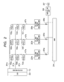
- FIG. 2 is a block diagram illustrating the solid-state imaging apparatus according to one embodiment of the present invention.
- FIG. 3 is a block diagram illustrating an imaging system in which the solid-state imaging apparatus according to the present invention is arranged.
- a pixel is constituted by an N-channel MOS transistor
- the present invention is also applicable to a case where the pixel is constituted by a P-channel MOS transistor. In this case, it only has to invert all polarities of voltages.
- FIG. 1 is a circuit diagram illustrating a pixel to be arranged in a solid-state imaging apparatus according to the first embodiment of the present invention.
- a pixel 100 includes a photodiode 101, a transfer MOS transistor 102, an FD (floating diffusion) 103, an amplifying MOS transistor 104, a reset MOS transistor 105, and a selection transistor 106.
- the photodiode 101 is one example of a photoelectric converting unit.
- the photoelectric converting unit only has to perform photoelectrical conversion for incident light.
- the transfer MOS transistor 102 transfers signal charges generated by the photoelectric conversion to the FD 103.
- the FD 103 is electrically connected to the gate of the amplifying MOS transistor 104.
- the amplifying MOS transistor 104 which constitutes a part of a source follower amplifier, outputs signals according to an amount of the signal charges transferred to the FD 103.
- the gate of the amplifying MOS transistor 104 is the input of the source follower amplifier.
- the reset MOS transistor 105 functions to reset the voltage of the FD 103 to a power supply voltage SVDD. Namely, in the present embodiment, the drain voltages of the amplifying MOS transistor 104 and the reset MOS transistor 105 are equivalent to the common power supply voltage SVDD.
- the selection transistor 106 selects a row from which signal charges should be output.
- the output of the source follower amplifier is connected to a vertical reading line 107, and a constant current source 108 is connected to the vertical reading line 107.
- the amplifying MOS transistor 104 and the constant current source 108 together constitute the source follower amplifier.
- a transfer MOS transistor driving line 109 is connected to the gate of the transfer MOS transistor 102, a reset MOS transistor driving line 110 is connected to the gate of the reset MOS transistor 105, and a selection transistor driving line 111 is connected to the gate of the selection transistor 106.
- the amplifying MOS transistor 104 is a buried-channel MOS transistor.
- P-type impurities are implanted into the semiconductor region near the interface of a gate insulating layer if necessary.
- the P-type impurity boron or the like can be used.
- N-type impurities are implanted into the semiconductor region which is below the semiconductor region into which the P-type impurities have been implanted.
- arsenic or the like can be used as the N-type impurity.
- the N-type semiconductor region is arranged at a deep position of the substrate as compared with the interface between the substrate and the gate insulating layer, the buried-channel MOS transistor can be established.
- the reset MOS transistor 105 and the selection transistor 106 may be the buried-channel MOS transistors respectively.
- a procedure of processes can be simplified. More specifically, in a case where ion implantation is performed to the channel portions of the respective transistors, the ion implantation concerned can be achieved by using a single mask, whereby manufacturing costs can be reduced.
- the transfer MOS transistor 102 which transfers the signal charges generated by the photoelectric conversion to the FD 103 is included in the pixel.
- a predetermined voltage is applied to the gate of the transfer MOS transistor 102 to make the transfer MOS transistor 102 in conduction state, whereby the signal charge in the photodiode 101 is transferred to the FD.
- complete depletion transfer is performed to the charge in the photodiode 101. That is, the constitution for performing the complete depletion transfer to the charge in the photodiode 101 is achieved by providing the transfer MOS transistor 102, whereby occurrence of a leak current in the photodiode 101 can be reduced.
- the driving block 112 supplies a signal, which is necessary for an imaging operation, to the pixel. More specifically, a pulse which is transferred from a vertical shift register is input to a terminal 113, and driving pulses are input to terminals 114, 115 and 116 respectively. Then, a logical operation to the pulse from the vertical shift register and the driving pulse is performed by each logical operation circuit which is included in the driving block 112. Subsequently, outputs from the logical operation circuits are input to driving circuits 117, 118 and 119 respectively.
- the driving circuit 117 supplies the signal to the gate of the reset MOS transistor 105
- the driving circuit 118 supplies the signal to the gate of the transfer MOS transistor 102
- the driving circuit 119 supplies the signal to the gate of the selection transistor 106.
- a voltage VresH is applied to the gate of the reset MOS transistor 105 in a case where the reset MOS transistor is in a conduction state
- a ground potential VSS is applied to the gate of the reset MOS transistor 105 in a case where the reset MOS transistor is in a non-conduction state
- a power supply voltage VDD is applied to the gates of the transfer MOS transistor 102 and the selection transistor 106 in a case where conduction arises in these transistors
- the ground potential VSS is applied to the gates of the transfer MOS transistor 102 and the selection transistor 106 in a case where conduction does not arise in these transistors.
- a negative voltage which is lower than the ground potential may be applied to the gate of the transfer MOS transistor 102 in the case where conduction does not arise in the transfer MOS transistor 102.
- the voltage which is applied to the gate refers the voltage which is applied to the gate of a transistor to make the transistor in a conduction state.
- the power supply voltage SVDD of the source follower amplifier is different from the power supply voltage VDD of the driving circuit which supplies the voltage to the gate of each transistor.
- the power supply voltage VDD is higher than the power supply voltage SVDD.
- the power supply voltage VDD may be the same as the power supply voltage SVDD or less.
- the present embodiment is characterized in that the voltage VresH which is applied to the gate of the reset MOS transistor is lower than the power supply voltage SVDD of the power supply.
- the drain of the amplifying MOS transistor and the drain of the reset MOS transistor are connected to the power supply. Moreover, it is desirable to set the voltage VresH to be lower than the power supply voltage VDD.
- FIG. 2 is a block diagram illustrating the solid-state imaging apparatus in which the pixel circuit illustrated in FIG. 1 is used.
- each of pixels 100a, 100b, 100c, 100d, 100e, 100f, 100g and 100i is equivalent to the pixel 100 illustrated in FIG. 1 .
- FIG. 2 shows an arrangement in which the pixels of 3 rows ⁇ 3 columns are arranged, the present invention is not limited to this. Namely, plural pixels may be arranged linearly or in matrix in the solid-state imaging apparatus.
- each of the horizontal driving lines 201a, 201b and 201c is equivalent to the transfer MOS transistor driving line 109, the reset MOS transistor driving line 110 and the selection transistor driving line 111 respectively illustrated in FIG. 1 .
- a VSR (vertical shift register) 202 is connected to the driving block 112.
- the detailed constitution of the driving block 112 is illustrated in FIG. 1 .
- Column signal reading units 203a, 203b and 203c are used to process the signals output from the pixels.
- An HSR (horizontal shift register) 204 generates a control signal to be used to sequentially read the pixel signals held by each of the column signal reading units 203a, 203b and 203c.
- the pixel signals are sequentially transferred to an amplifying unit 206 by selecting switches 205a, 205b and 205c. Then, the pixel signal is amplified by the amplifying unit 206, and the amplified signal is output from an output terminal 207.
- the voltage VresH is applied to the gate of the reset MOS transistor 105 in the case where conduction arises in the reset MOS transistor 105.
- the driving circuit 117 which supplies the voltage to the gate of the reset MOS transistor 105 is constituted by an inverter circuit, and the power supply voltage of the inverter circuit concerned is given as VresH.
- the power supply voltage VresH is lower than the power supply voltage SVDD to be supplied to the drain of the reset MOS transistor 105.
- VGS VresH - Vth_res
- the gate voltage VGS of the amplifying MOS transistor 104 decreases.
- the power supply voltage SVDD is applied to the drain of the amplifying MOS transistor 104.
- a threshold voltage of the amplifying MOS transistor is given as Vth_sf. SVDD ⁇ VGS - Vth_sf
- the voltage VresH which is applied to the gate of the reset MOS transistor may satisfy the following expression (3) which is obtained from the expressions (1) and (2).
- the voltage VresH is lower than the sum of the drain voltage SVDD of the amplifying MOS transistor, the threshold voltage Vth_sf of the amplifying MOS transistor and the threshold voltage Vth_res of the reset MOS transistor.
- the amplifying MOS transistor 104 can easily operate in the saturation region. Further, since there is provided the driving circuit which supplies the signals by which the voltages at the time of conduction satisfy the conditions given by the expression (3) and (4), the solid-state imaging apparatus of which the linearity is more excellent and satisfactory can be obtained.
- the power supply voltage SVDD of the power supply which is connected to the drain of the reset MOS transistor 105 is 4.8V
- the voltage VDD which is applied to each of the gates of the transfer MOS transistor 102 and the selection transistor 106 in the case conduction arises in each of these transistors is 5.0V
- each of the threshold voltage Vth_sf of the amplifying MOS transistor 104 and the threshold voltage Vth_res of the reset MOS transistor 105 is -0.2V
- the voltage VresH which is applied to the gate of the reset MOS transistor 105 in the case where conduction arises in this transistor is 3.8V.
- the threshold voltage Vth_sf of the amplifying MOS transistor has a value close to 0V or becomes a negative voltage.
- the threshold voltage Vth_res of the reset MOS transistor likewise has a value close to 0V or becomes a negative voltage.
- the drain voltage of the reset MOS transistor 105 and the drain voltage of the amplifying MOS transistor 104 are common to each other. Namely, the number of wirings can be reduced by connecting the respective drains to the common power supply wiring.
- the photodiode 101, the transfer MOS transistor 102, the FD 103, the amplifying MOS transistor 104, the reset MOS transistor 105 and the selection transistor 106 which are included in one pixel are formed on a pixel region of a semiconductor substrate. Further, the pixel regions are arranged linearly or in matrix on the semiconductor substrate. Incidentally, a device separating portion may be arranged between the pixel regions.
- the drain of the amplifying MOS transistor 104 and the drain of the reset MOS transistor 105 are connected to the single wiring which is arranged on the pixel region through an insulating film.
- a substantial aperture ratio of the photoelectric converting unit can be improved.
- the drain voltage of the reset MOS transistor 105 may be supplied independently of the drain voltage of the amplifying MOS transistor 104.
- a constitution in which the gate potential is higher than or equal to the drain potential when conduction arises in the reset MOS transistor will be described as a comparative example.
- a voltage which is substantially the same as the drain voltage of the reset MOS transistor is supplied to the gate of the amplifying MOS transistor which constitutes the source follower amplifier. If the common power supply voltage SVDD is supplied to the drain of the reset MOS transistor and the drain of the amplifying MOS transistor, SVDD ⁇ VGS is obtained in the expression (2). For this reason, in order to satisfy the condition that the amplifying MOS transistor operates in the saturation region, or in order to satisfy the expression (2), the threshold voltage Vth has to be a positive voltage.
- the buried-channel MOS transistor of which the threshold voltage Vth is negative does not operate in the saturation region. Further, even if the average value of the threshold voltages Vth of the plural pixels is positive, there is a possibility that the threshold voltages Vth of the amplifying MOS transistors of the partial pixels are negative because of a variation of devices due to a manufacturing process and the like. For this reason, linearity cannot be improved by the constitution of the comparative example.
- the voltage which is applied to the gate of the reset MOS transistor is lower than the power supply voltage VDD.
- the buried-channel MOS transistor which is used for the source follower amplifier operates easily in the saturation region.
- a voltage which is applied to the gate of the reset MOS transistor 105 is not decreased. Instead, a threshold voltage Vth of the reset MOS transistor 105 is increased. More specifically, the power supply of the driving circuit 117 is set to have a power supply voltage VDD, so that the voltage to be applied to the gate of the reset MOS transistor 105 is set to the power supply voltage VDD.
- the threshold voltage Vth of the reset MOS transistor 105 is set to satisfy the following expression (5) which is obtained by substituting the power supply voltage VDD to the threshold voltage VresH in the expression (3).
- the threshold voltage Vth_res of the reset MOS transistor 105 is equal to or higher than 0.2V.
- the threshold value of the reset MOS transistor 105 is the value which satisfies the expression (5).
- FIG. 3 is a block diagram illustrating a digital still camera as an example of the imaging system.
- a barrier 1 is used to protect a lens 2, and the lens 2 provides an optical image of a subject on a solid-state imaging apparatus 4.
- a diaphragm 3 varies an amount of light which passed through the lens 2, and the solid-state imaging apparatus 4, which has been described in the above embodiments, converts the optical image provided by the lens 2 into image data.
- an A/D (analog-to-digital) converter is provided on the substrate of the solid-state imaging apparatus 4.
- a signal processing unit 7 performs various processes such as a correction process, a compression process and the like to the image data output from the solid-state imaging apparatus 4, a timing generation unit 8 generates timing signals to the solid-state imaging apparatus 4 and the signal processing unit 7, an overall controlling/calculating unit 9 which performs various calculations and controls the overall of the digital still camera, a memory unit 10 is used to temporarily store the image data, a recording medium control I/F (interface) unit 11 is used to perform recording or reading to a recording medium 12, the recording medium 12 such as a detachably provided semiconductor memory or the like is used to record and/or read the image data, and an external I/F unit 13 is used to perform communication with an external computer and the like.
- the timing signal or the like may be input from the outside of the imaging system, and the imaging system only has to provide at least the solid-state imaging apparatus 4 and the signal processing unit 7 for processing the image signal output from the solid-state imaging apparatus 4.
- the solid-state imaging apparatus 4 and the A/D converter are provided on the same substrate.
- the solid-state imaging apparatus 4 and the A/D converter may be provided respectively on different substrates.
- the solid-state imaging apparatus 4 and the signal processing unit 7 may be provided on the same substrate.
- the solid-state imaging apparatus according to the present invention can be applied to the camera system. That is, if the solid-state imaging apparatus according to the present invention is applied to the camera system, an image in which in which linearity is excellent and satisfactory and noises are reduced can be taken.
- the pixel is exemplarily constituted by the N-channel MOS transistor.
- the present invention is also applicable to a case where the pixel is constituted by a P-channel MOS transistor.
- the amplifying MOS transistor is constituted by the P-channel MOS transistor, the 1/f noise is reduced as compared with the case where the N-channel MOS transistor is used.
- the pixel in the case where the pixel is constituted by the P-channel MOS transistor, it only has to invert all the polarities of the voltages. That is, a ground potential SVSS is applied to the drain of the reset MOS transistor and the drain of the amplifying MOS transistor.
- a power supply voltage SVSS of the power supply to which the drain of the reset MOS transistor and the drain of the amplifying MOS transistor are connected is a negative voltage which is lower than the ground potential.
- the voltage VSS which is applied to the date of each transistor in the case where conduction arises in the transistor concerned is a negative voltage which is lower than the ground potential.
- the pixel is constituted by the P-channel MOS transistor
- a voltage which is higher than the voltage to be applied to the drain of the amplifying MOS transistor is applied to the gate of the reset MOS transistor.
- the power supply voltage SVDD is replaced by the drain voltage SVSS, and the direction of the inequality sign is inverted.
- the amplifying MOS transistor is the P-type buried-channel MOS transistor
- the threshold voltage shifts from a negative voltage to a positive voltage.
- the P-channel MOS transistor As a concrete constitution by which the P-channel MOS transistor is applied to the pixel, a constitution in which holes are collected as signal charges is conceivable. In such a case, all the transistors in the pixels can be constituted by the P-channel MOS transistors. As a result, since all the MOS transistors of the pixels can be formed in an N-type well, the pixel can easily be made fine. Besides, the amplifying MOS transistor which is constituted by the P-channel MOS transistor may be arranged in the N-type well by using electrons as the signal charges.
- the transfer MOS transistor is formed in a P-type well, for example, a back-illuminated constitution in which circuits to be arranged at the stage subsequent to the floating diffusion are formed on a substrate which is different from the photoelectric converting unit is conceived in case of making the pixel fine.
- a solid-state imaging apparatus is characterized in that a reset gate voltage VresH to be applied to a gate of a reset MOS transistor is lower than a power supply voltage SVDD of a power supply to which drains of an amplifying MOS transistor and the reset MOS transistor are connected.
Landscapes
- Solid State Image Pick-Up Elements (AREA)
- Transforming Light Signals Into Electric Signals (AREA)
Abstract
Description
- The present invention relates to a solid-state imaging apparatus and an imaging system.
- In an APS (active pixel sensor) type solid-state imaging apparatus, an amplifying unit such as a source follower amplifier or the like is provided in each of pixels. Here, a 1/f noise or an RTS (random telegraph signal) noise which arises in a MOS (metal oxide semiconductor) transistor used for the amplifying unit causes noises in the amplifying unit. Here, in Japanese Patent Application Laid-Open No.
2005-286168 - Incidentally, Japanese Patent Application Laid-Open No.
2000-244818 - In order to reduce the 1/f noise or the RTS noise, it is effective to form the channel of the amplifying MOS transistor, which constitutes the source follower amplifier, at a position which is deep from the surface of the semiconductor. However, if the channel is formed at the deep position, a threshold voltage decreases (in a case of an N-channel MOS transistor). As a result, there is a case where the amplifying MOS transistor which constitutes the source follower amplifier operates in a region other than a saturation region. Alternatively, there is a case where the amplifying MOS transistor operates in a transition region between the saturation region and a linear region. Here, if the MOS transistor operates in the linear region, linearity of an output signal from the source follower amplifier deteriorates. In particular, in a case where the amplifying MOS transistor is arranged for each pixel or for plural pixels, there is a possibility that the amplifying MOS transistor which operates in the saturation region and the MOS transistor which operates in the linear region coexist due to a variation of these devices.
- In consideration of such a problem as described above, the present invention aims to provide a solid-state imaging apparatus which can secure excellent and satisfactory linearity and also can reduce noises.
- A solid-state imaging apparatus according to the present invention is characterized by an apparatus which has plural pixels each comprising: a photoelectric converting unit configured to perform photoelectric conversion of incident light; an amplifying MOS transistor configured to output a signal based on a charge generated by the photoelectric converting unit; and a reset MOS transistor configured to reset a gate potential of the amplifying MOS transistor, wherein the amplifying MOS transistor is an N-type buried-channel MOS transistor, and a voltage to be applied to a gate of the reset MOS transistor for setting the reset MOS transistor in a conduction state is lower than a voltage to be applied to a drain of the reset MOS transistor.
- According to the present invention, it is possible to provide the solid-state imaging apparatus in which linearity is excellent and satisfactory and noises are reduced.
- Further features and aspects of the present invention will become apparent from the following detailed description of exemplary embodiments with reference to the attached drawings.
-
FIG. 1 is a circuit diagram illustrating a pixel to be arranged in a solid-state imaging apparatus according to one embodiment of the present invention. -
FIG. 2 is a block diagram illustrating the solid-state imaging apparatus according to one embodiment of the present invention. -
FIG. 3 is a block diagram illustrating an imaging system in which the solid-state imaging apparatus according to the present invention is arranged. - Hereinafter, exemplary embodiments of the present invention will be described with reference to the attached drawings. In the following description, an example that a pixel is constituted by an N-channel MOS transistor will be explained. However, it should be noted that the present invention is also applicable to a case where the pixel is constituted by a P-channel MOS transistor. In this case, it only has to invert all polarities of voltages.
-
FIG. 1 is a circuit diagram illustrating a pixel to be arranged in a solid-state imaging apparatus according to the first embodiment of the present invention. In the present embodiment, apixel 100 includes aphotodiode 101, atransfer MOS transistor 102, an FD (floating diffusion) 103, an amplifyingMOS transistor 104, areset MOS transistor 105, and aselection transistor 106. - Here, the
photodiode 101 is one example of a photoelectric converting unit. The photoelectric converting unit only has to perform photoelectrical conversion for incident light. Thetransfer MOS transistor 102 transfers signal charges generated by the photoelectric conversion to theFD 103. The FD 103 is electrically connected to the gate of the amplifyingMOS transistor 104. The amplifyingMOS transistor 104, which constitutes a part of a source follower amplifier, outputs signals according to an amount of the signal charges transferred to theFD 103. Here, the gate of the amplifyingMOS transistor 104 is the input of the source follower amplifier. The resetMOS transistor 105 functions to reset the voltage of theFD 103 to a power supply voltage SVDD. Namely, in the present embodiment, the drain voltages of the amplifyingMOS transistor 104 and thereset MOS transistor 105 are equivalent to the common power supply voltage SVDD. Theselection transistor 106 selects a row from which signal charges should be output. - The output of the source follower amplifier is connected to a
vertical reading line 107, and a constantcurrent source 108 is connected to thevertical reading line 107. Thus, the amplifyingMOS transistor 104 and the constantcurrent source 108 together constitute the source follower amplifier. - A transfer MOS
transistor driving line 109 is connected to the gate of thetransfer MOS transistor 102, a reset MOStransistor driving line 110 is connected to the gate of thereset MOS transistor 105, and a selectiontransistor driving line 111 is connected to the gate of theselection transistor 106. - Incidentally, the amplifying
MOS transistor 104 is a buried-channel MOS transistor. Here, one example of a method of forming the buried-channel MOS transistor will be described. That is, P-type impurities are implanted into the semiconductor region near the interface of a gate insulating layer if necessary. As the P-type impurity, boron or the like can be used. Next, N-type impurities are implanted into the semiconductor region which is below the semiconductor region into which the P-type impurities have been implanted. Here, as the N-type impurity, arsenic or the like can be used. In any case, since the N-type semiconductor region is arranged at a deep position of the substrate as compared with the interface between the substrate and the gate insulating layer, the buried-channel MOS transistor can be established. - In the present embodiment, the
reset MOS transistor 105 and theselection transistor 106 may be the buried-channel MOS transistors respectively. In particular, in a case where threshold voltage characteristics of thereset MOS transistor 105 and theselection transistor 106 match with a threshold voltage characteristic of the amplifyingMOS transistor 104, a procedure of processes can be simplified. More specifically, in a case where ion implantation is performed to the channel portions of the respective transistors, the ion implantation concerned can be achieved by using a single mask, whereby manufacturing costs can be reduced. - In the present embodiment, the
transfer MOS transistor 102 which transfers the signal charges generated by the photoelectric conversion to theFD 103 is included in the pixel. Thus, a predetermined voltage is applied to the gate of thetransfer MOS transistor 102 to make thetransfer MOS transistor 102 in conduction state, whereby the signal charge in thephotodiode 101 is transferred to the FD. More desirably, complete depletion transfer is performed to the charge in thephotodiode 101. That is, the constitution for performing the complete depletion transfer to the charge in thephotodiode 101 is achieved by providing thetransfer MOS transistor 102, whereby occurrence of a leak current in thephotodiode 101 can be reduced. - Subsequently, the detail of a
driving block 112 will be described. Thedriving block 112 supplies a signal, which is necessary for an imaging operation, to the pixel. More specifically, a pulse which is transferred from a vertical shift register is input to aterminal 113, and driving pulses are input toterminals driving block 112. Subsequently, outputs from the logical operation circuits are input to drivingcircuits driving circuit 117 supplies the signal to the gate of thereset MOS transistor 105, thedriving circuit 118 supplies the signal to the gate of thetransfer MOS transistor 102, and thedriving circuit 119 supplies the signal to the gate of theselection transistor 106. - Incidentally, a voltage VresH is applied to the gate of the
reset MOS transistor 105 in a case where the reset MOS transistor is in a conduction state, and a ground potential VSS is applied to the gate of thereset MOS transistor 105 in a case where the reset MOS transistor is in a non-conduction state. Further, a power supply voltage VDD is applied to the gates of thetransfer MOS transistor 102 and theselection transistor 106 in a case where conduction arises in these transistors, and the ground potential VSS is applied to the gates of thetransfer MOS transistor 102 and theselection transistor 106 in a case where conduction does not arise in these transistors. In order to suppress a dark current in the photodiode, a negative voltage which is lower than the ground potential may be applied to the gate of thetransfer MOS transistor 102 in the case where conduction does not arise in thetransfer MOS transistor 102. In the following description, unless otherwise noted, the voltage which is applied to the gate refers the voltage which is applied to the gate of a transistor to make the transistor in a conduction state.. - It should be noted that the power supply voltage SVDD of the source follower amplifier is different from the power supply voltage VDD of the driving circuit which supplies the voltage to the gate of each transistor. In general, the power supply voltage VDD is higher than the power supply voltage SVDD. However, the power supply voltage VDD may be the same as the power supply voltage SVDD or less.
- The present embodiment is characterized in that the voltage VresH which is applied to the gate of the reset MOS transistor is lower than the power supply voltage SVDD of the power supply. The drain of the amplifying MOS transistor and the drain of the reset MOS transistor are connected to the power supply. Moreover, it is desirable to set the voltage VresH to be lower than the power supply voltage VDD.
-
FIG. 2 is a block diagram illustrating the solid-state imaging apparatus in which the pixel circuit illustrated inFIG. 1 is used. InFIG. 2 , each ofpixels pixel 100 illustrated inFIG. 1 . AlthoughFIG. 2 shows an arrangement in which the pixels of 3 rows × 3 columns are arranged, the present invention is not limited to this. Namely, plural pixels may be arranged linearly or in matrix in the solid-state imaging apparatus. - In the drawing,
vertical reading lines pixels 100a to 100i, and each ofhorizontal driving lines horizontal driving lines transistor driving line 109, the reset MOStransistor driving line 110 and the selectiontransistor driving line 111 respectively illustrated inFIG. 1 . Further, a VSR (vertical shift register) 202 is connected to thedriving block 112. Here, the detailed constitution of the drivingblock 112 is illustrated inFIG. 1 . - Column
signal reading units signal reading units amplifying unit 206 by selectingswitches unit 206, and the amplified signal is output from anoutput terminal 207. - In the present embodiment, the voltage VresH is applied to the gate of the
reset MOS transistor 105 in the case where conduction arises in thereset MOS transistor 105. More specifically, the drivingcircuit 117 which supplies the voltage to the gate of thereset MOS transistor 105 is constituted by an inverter circuit, and the power supply voltage of the inverter circuit concerned is given as VresH. Here, it should be noted that the power supply voltage VresH is lower than the power supply voltage SVDD to be supplied to the drain of thereset MOS transistor 105. - If the voltage to be applied to the gate of the
reset MOS transistor 105 is given as VresH, a voltage VGS at the gate of the amplifyingMOS transistor 104 is given by the following expression (1). Here, it is assumed that a threshold voltage of thereset MOS transistor 105 is given as Vth_res.
- As indicated by the expression (1), in a case where the voltage to be applied to the gate of the
reset MOS transistor 105 decreases, the gate voltage VGS of the amplifyingMOS transistor 104 decreases. - The power supply voltage SVDD is applied to the drain of the amplifying
MOS transistor 104. Thus, to satisfy a condition that the amplifyingMOS transistor 104 operates in a saturation region, it only has to satisfy the following expression (2). Here, it is assumed that a threshold voltage of the amplifying MOS transistor is given as Vth_sf.
- Therefore, if the gate voltage VGS of the amplifying
MOS transistor 104 decreases, the value of the right member of the expression (2) decreases, whereby the operation of the amplifyingMOS transistor 104 comes close to the operation in the saturation region. - More desirably, the voltage VresH which is applied to the gate of the reset MOS transistor may satisfy the following expression (3) which is obtained from the expressions (1) and (2).

- That is, it is desirable that the voltage VresH is lower than the sum of the drain voltage SVDD of the amplifying MOS transistor, the threshold voltage Vth_sf of the amplifying MOS transistor and the threshold voltage Vth_res of the reset MOS transistor.
- Further, to satisfy a condition that conduction arises in the
reset MOS transistor 105, it is necessary to satisfy the following expression (4).
- As just described, since the voltage VresH is lower than the power supply voltage VDD, the amplifying
MOS transistor 104 can easily operate in the saturation region. Further, since there is provided the driving circuit which supplies the signals by which the voltages at the time of conduction satisfy the conditions given by the expression (3) and (4), the solid-state imaging apparatus of which the linearity is more excellent and satisfactory can be obtained. - In the present embodiment, the power supply voltage SVDD of the power supply which is connected to the drain of the
reset MOS transistor 105 is 4.8V, the voltage VDD which is applied to each of the gates of thetransfer MOS transistor 102 and theselection transistor 106 in the case conduction arises in each of these transistors is 5.0V, each of the threshold voltage Vth_sf of the amplifyingMOS transistor 104 and the threshold voltage Vth_res of thereset MOS transistor 105 is -0.2V, and the voltage VresH which is applied to the gate of thereset MOS transistor 105 in the case where conduction arises in this transistor is 3.8V. - In a case where a buried-channel MOS transistor is used for the source follower amplifier to reduce a 1/f noise or an RTS noise, the threshold voltage Vth_sf of the amplifying MOS transistor has a value close to 0V or becomes a negative voltage. Further, in a case where a buried-channel MOS transistor is used also for the reset transistor, the threshold voltage Vth_res of the reset MOS transistor likewise has a value close to 0V or becomes a negative voltage. Furthermore, if the buried-channel is formed at the deep position to improve a noise reduction effect, the threshold voltage shifts toward the negative direction. According to this, it is desirable that the voltage VresH is lower.
- In the present embodiment, even in a case where the noise is reduced by applying the buried-channel MOS transistor to the amplifying
MOS transistor 104 or the like, excellent and satisfactory linearity can be secured by lowering the voltage VresH. - Further, in the present embodiment, the drain voltage of the
reset MOS transistor 105 and the drain voltage of the amplifyingMOS transistor 104 are common to each other. Namely, the number of wirings can be reduced by connecting the respective drains to the common power supply wiring. - The
photodiode 101, thetransfer MOS transistor 102, theFD 103, the amplifyingMOS transistor 104, thereset MOS transistor 105 and theselection transistor 106 which are included in one pixel are formed on a pixel region of a semiconductor substrate. Further, the pixel regions are arranged linearly or in matrix on the semiconductor substrate. Incidentally, a device separating portion may be arranged between the pixel regions. - The drain of the amplifying
MOS transistor 104 and the drain of thereset MOS transistor 105 are connected to the single wiring which is arranged on the pixel region through an insulating film. Thus, a substantial aperture ratio of the photoelectric converting unit can be improved. - Incidentally, in the present embodiment, the drain voltage of the
reset MOS transistor 105 may be supplied independently of the drain voltage of the amplifyingMOS transistor 104. - Subsequently, a constitution in which the gate potential is higher than or equal to the drain potential when conduction arises in the reset MOS transistor will be described as a comparative example. In such a case, a voltage which is substantially the same as the drain voltage of the reset MOS transistor is supplied to the gate of the amplifying MOS transistor which constitutes the source follower amplifier. If the common power supply voltage SVDD is supplied to the drain of the reset MOS transistor and the drain of the amplifying MOS transistor, SVDD ≈ VGS is obtained in the expression (2). For this reason, in order to satisfy the condition that the amplifying MOS transistor operates in the saturation region, or in order to satisfy the expression (2), the threshold voltage Vth has to be a positive voltage. For this reason, the buried-channel MOS transistor of which the threshold voltage Vth is negative does not operate in the saturation region. Further, even if the average value of the threshold voltages Vth of the plural pixels is positive, there is a possibility that the threshold voltages Vth of the amplifying MOS transistors of the partial pixels are negative because of a variation of devices due to a manufacturing process and the like. For this reason, linearity cannot be improved by the constitution of the comparative example.
- As just described, in the present embodiment, the voltage which is applied to the gate of the reset MOS transistor is lower than the power supply voltage VDD. For this reason, the buried-channel MOS transistor which is used for the source follower amplifier operates easily in the saturation region. Thus, according to the constitution like this, it is possible to reduce noises as improving linearity.
- (Second Embodiment)
- Subsequently, the solid-state imaging apparatus according to the second embodiment of the present invention will be described. In the present embodiment, a voltage which is applied to the gate of the
reset MOS transistor 105 is not decreased. Instead, a threshold voltage Vth of thereset MOS transistor 105 is increased. More specifically, the power supply of the drivingcircuit 117 is set to have a power supply voltage VDD, so that the voltage to be applied to the gate of thereset MOS transistor 105 is set to the power supply voltage VDD. - To decrease a gate voltage VGS of the amplifying
MOS transistor 104, the threshold voltage Vth of thereset MOS transistor 105 is set to satisfy the following expression (5) which is obtained by substituting the power supply voltage VDD to the threshold voltage VresH in the expression (3).
- Here, if it is assumed that the power supply voltage VDD is 5.0V, the power supply voltage SVDD is 4.8V, and the threshold voltage Vth_sf of the amplifying
MOS transistor 104 is 0V, then the threshold voltage Vth_res of thereset MOS transistor 105 is equal to or higher than 0.2V. However, in consideration of a variation of characteristics of the MOS transistors and the like, it is desirable to set the threshold voltage Vth_res to be equal to or higher than 0.4V, and it is further desirable to set the threshold voltage Vth_res to be equal to or higher than 0.6V. - In the present embodiment, the threshold value of the
reset MOS transistor 105 is the value which satisfies the expression (5). By such a constitution, the buried-channel MOS transistor which is used for the source follower amplifier operates easily in the saturation region. Thus, it is possible to reduce noises as improving linearity. - Hereinafter, the third embodiment of the present invention in which the solid-state imaging apparatus according to the present invention is applied to a camera system will be described in detail. Here, it should be noted that, as an imaging system, a digital still camera, a digital camcorder or the like can be used.
FIG. 3 is a block diagram illustrating a digital still camera as an example of the imaging system. - In
FIG. 3 , a barrier 1 is used to protect alens 2, and thelens 2 provides an optical image of a subject on a solid-state imaging apparatus 4. Adiaphragm 3 varies an amount of light which passed through thelens 2, and the solid-state imaging apparatus 4, which has been described in the above embodiments, converts the optical image provided by thelens 2 into image data. Here, an A/D (analog-to-digital) converter is provided on the substrate of the solid-state imaging apparatus 4. Asignal processing unit 7 performs various processes such as a correction process, a compression process and the like to the image data output from the solid-state imaging apparatus 4, atiming generation unit 8 generates timing signals to the solid-state imaging apparatus 4 and thesignal processing unit 7, an overall controlling/calculatingunit 9 which performs various calculations and controls the overall of the digital still camera, amemory unit 10 is used to temporarily store the image data, a recording medium control I/F (interface)unit 11 is used to perform recording or reading to arecording medium 12, therecording medium 12 such as a detachably provided semiconductor memory or the like is used to record and/or read the image data, and an external I/F unit 13 is used to perform communication with an external computer and the like. Here, the timing signal or the like may be input from the outside of the imaging system, and the imaging system only has to provide at least the solid-state imaging apparatus 4 and thesignal processing unit 7 for processing the image signal output from the solid-state imaging apparatus 4. - In the present embodiment, the solid-state imaging apparatus 4 and the A/D converter are provided on the same substrate. However, the solid-state imaging apparatus 4 and the A/D converter may be provided respectively on different substrates. Moreover, the solid-state imaging apparatus 4 and the
signal processing unit 7 may be provided on the same substrate. - As described above, the solid-state imaging apparatus according to the present invention can be applied to the camera system. That is, if the solid-state imaging apparatus according to the present invention is applied to the camera system, an image in which in which linearity is excellent and satisfactory and noises are reduced can be taken.
- In the above description, the pixel is exemplarily constituted by the N-channel MOS transistor. However, the present invention is also applicable to a case where the pixel is constituted by a P-channel MOS transistor. In this case, since the amplifying MOS transistor is constituted by the P-channel MOS transistor, the 1/f noise is reduced as compared with the case where the N-channel MOS transistor is used.
- In any case, in the case where the pixel is constituted by the P-channel MOS transistor, it only has to invert all the polarities of the voltages. That is, a ground potential SVSS is applied to the drain of the reset MOS transistor and the drain of the amplifying MOS transistor.
- Also, another constitution can be adopted. In this constitution, a power supply voltage SVSS of the power supply to which the drain of the reset MOS transistor and the drain of the amplifying MOS transistor are connected is a negative voltage which is lower than the ground potential. At this time, the voltage VSS which is applied to the date of each transistor in the case where conduction arises in the transistor concerned is a negative voltage which is lower than the ground potential.
- In the case where the pixel is constituted by the P-channel MOS transistor, a voltage which is higher than the voltage to be applied to the drain of the amplifying MOS transistor is applied to the gate of the reset MOS transistor. Moreover, in each of the above-described expressions (1) to (5), the power supply voltage SVDD is replaced by the drain voltage SVSS, and the direction of the inequality sign is inverted. In the case where the amplifying MOS transistor is the P-type buried-channel MOS transistor, the threshold voltage shifts from a negative voltage to a positive voltage.
- As a concrete constitution by which the P-channel MOS transistor is applied to the pixel, a constitution in which holes are collected as signal charges is conceivable. In such a case, all the transistors in the pixels can be constituted by the P-channel MOS transistors. As a result, since all the MOS transistors of the pixels can be formed in an N-type well, the pixel can easily be made fine. Besides, the amplifying MOS transistor which is constituted by the P-channel MOS transistor may be arranged in the N-type well by using electrons as the signal charges. In such a case, since the transfer MOS transistor is formed in a P-type well, for example, a back-illuminated constitution in which circuits to be arranged at the stage subsequent to the floating diffusion are formed on a substrate which is different from the photoelectric converting unit is conceived in case of making the pixel fine.
- While the present invention has been described with reference to the exemplary embodiments, it is to be understood that the invention is not limited to the disclosed exemplary embodiments. The scope of the following claims is to be accorded the broadest interpretation so as to encompass all such modifications and equivalent structures and functions.
A solid-state imaging apparatus according to the present invention is characterized in that a reset gate voltage VresH to be applied to a gate of a reset MOS transistor is lower than a power supply voltage SVDD of a power supply to which drains of an amplifying MOS transistor and the reset MOS transistor are connected.
Claims (15)
- A solid-state imaging apparatus which has plural pixels each comprising:a photoelectric converting unit configured to perform photoelectric conversion of incident light;an amplifying MOS (metal oxide semiconductor) transistor configured to output a signal based on a charge generated by the photoelectric converting unit; anda reset MOS transistor configured to reset a gate potential of the amplifying MOS transistor,wherein the amplifying MOS transistor is an N-type buried-channel MOS transistor, anda voltage to be applied to a gate of the reset MOS transistor for setting the reset MOS transistor in a conduction state is lower than a voltage to be applied to a drain of the reset MOS transistor.
- The solid-state imaging apparatus according to Claim 1, wherein the voltage (VresH) to be applied to the gate of the reset MOS transistor for setting the reset MOS transistor in the conduction state, a drain voltage (SVDD) of the amplifying MOS transistor, a threshold voltage (Vth_sf) of the amplifying MOS transistor, and a threshold voltage (Vth_res) of the reset MOS transistor satisfy following two expressions:


- The solid-state imaging apparatus according to Claim 1, wherein
the reset MOS transistor is a buried-channel MOS transistor, and
a threshold voltage of the reset MOS transistor is a negative voltage. - The solid-state imaging apparatus according to Claim 1, wherein a threshold voltage of the amplifying MOS transistor is a negative voltage.
- The solid-state imaging apparatus according to Claim 1, wherein
the pixel further includes a transfer MOS transistor and a floating diffusion, and
the transfer MOS transistor transfers the charge generated by the photoelectric converting unit to the floating diffusion. - The solid-state imaging apparatus according to Claim 1, wherein a drain of the amplifying MOS transistor and the drain of the reset MOS transistor are connected to a single power supply wiring which is arranged within a pixel region.
- A solid-state imaging apparatus which has plural pixels each comprising:a photoelectric converting unit configured to perform photoelectric conversion of incident light;an amplifying MOS transistor configured to output a signal based on a charge generated by the photoelectric converting unit; anda reset MOS transistor configured to reset a gate potential of the amplifying MOS transistor,wherein the amplifying MOS transistor is a P-type buried-channel MOS transistor, anda voltage to be applied to a gate of the reset MOS transistor for setting the reset MOS transistor in a conduction state is higher than a voltage to be applied to a drain of the reset MOS transistor.
- The solid-state imaging apparatus according to Claim 7, wherein the voltage (VresH) to be applied to the gate of the reset MOS transistor for setting the reset MOS transistor in the conduction state, a drain voltage (SVSS) of the amplifying MOS transistor, a threshold voltage (Vth_sf) of the amplifying MOS transistor, and a threshold voltage (Vth_res) of the reset MOS transistor satisfy following two expressions:


- The solid-state imaging apparatus according to Claim 7, wherein
the reset MOS transistor is a buried-channel MOS transistor, and
a threshold voltage of the reset MOS transistor is a positive voltage. - The solid-state imaging apparatus according to Claim 7, wherein a threshold voltage of the amplifying MOS transistor is a positive voltage.
- The solid-state imaging apparatus according to Claim 7, wherein
the pixel further includes a transfer MOS transistor and a floating diffusion, and
the transfer MOS transistor transfers the charge generated by the photoelectric converting unit to the floating diffusion. - The solid-state imaging apparatus according to Claim 7, wherein a drain of the amplifying MOS transistor and the drain of the reset MOS transistor are connected to a single power supply wiring which is arranged within a pixel region.
- A solid-state imaging apparatus which has plural pixels each comprising:a photoelectric converting unit configured to perform photoelectric conversion of incident light;an amplifying MOS transistor configured to output a signal based on a charge generated by the photoelectric converting unit; anda reset MOS transistor configured to reset a gate potential of the amplifying MOS transistor,wherein the amplifying MOS transistor is an N-type buried-channel MOS transistor, anda threshold voltage (Vth_res) of the reset MOS transistor, a voltage (VDD) to be applied to a gate of the reset MOS transistor for setting the reset MOS transistor in a conduction state, a voltage (SVDD) to be applied to a drain of the reset MOS transistor, and a threshold voltage (Vth_sf) of the amplifying MOS transistor satisfy a following expression:

- A solid-state imaging apparatus which has plural pixels each comprising:a photoelectric converting unit configured to perform photoelectric conversion of incident light;an amplifying MOS transistor configured to output a signal based on a charge generated by the photoelectric converting unit; anda reset MOS transistor configured to reset a gate potential of the amplifying MOS transistor,wherein the amplifying MOS transistor is a P-type buried-channel MOS transistor, anda threshold voltage (Vth_res) of the reset MOS transistor, a voltage (VSS) to be applied to a gate of the reset MOS transistor for setting the reset MOS transistor in a conduction state, a voltage (SVSS) to be applied to a drain of the reset MOS transistor, and a threshold voltage (Vth_sf) of the amplifying MOS transistor satisfy a following expression:

- An imaging system comprising:the solid-state imaging apparatus to any one of the preceding claims; anda signal processing unit configured to process an imaging signal output from the solid-state imaging apparatus.
Applications Claiming Priority (1)
| Application Number | Priority Date | Filing Date | Title |
|---|---|---|---|
| JP2009295442A JP5538876B2 (en) | 2009-12-25 | 2009-12-25 | Solid-state imaging device |
Publications (2)
| Publication Number | Publication Date |
|---|---|
| EP2339629A2 true EP2339629A2 (en) | 2011-06-29 |
| EP2339629A3 EP2339629A3 (en) | 2012-05-23 |
Family
ID=43877076
Family Applications (1)
| Application Number | Title | Priority Date | Filing Date |
|---|---|---|---|
| EP10194854A Withdrawn EP2339629A3 (en) | 2009-12-25 | 2010-12-14 | Solid-state imaging apparatus |
Country Status (4)
| Country | Link |
|---|---|
| US (1) | US8525896B2 (en) |
| EP (1) | EP2339629A3 (en) |
| JP (1) | JP5538876B2 (en) |
| CN (1) | CN102110701B (en) |
Cited By (1)
| Publication number | Priority date | Publication date | Assignee | Title |
|---|---|---|---|---|
| CN103716559A (en) * | 2014-01-13 | 2014-04-09 | 中国科学院上海高等研究院 | Pixel unit readout device and method and pixel array readout device and method |
Families Citing this family (14)
| Publication number | Priority date | Publication date | Assignee | Title |
|---|---|---|---|---|
| US9891102B2 (en) | 2010-04-22 | 2018-02-13 | Samsung Electronics Co., Ltd. | Simplified light sensing circuit, light sensing apparatus including the light sensing circuit, method of driving the light sensing apparatus, and image acquisition apparatus and optical touch screen apparatus including the light sensing apparatus |
| KR102056905B1 (en) * | 2011-07-25 | 2019-12-18 | 삼성전자주식회사 | Light sensing apparatus and method of driving the light sensing apparatus, and optical touch screen apparatus including the light sensing apparatus |
| US8445828B2 (en) | 2010-07-01 | 2013-05-21 | Silicon Optronics, Inc. | High dynamic range image sensor with in pixel memory |
| WO2013027524A1 (en) * | 2011-08-24 | 2013-02-28 | シャープ株式会社 | Solid-state imaging element |
| JP5864990B2 (en) | 2011-10-03 | 2016-02-17 | キヤノン株式会社 | Solid-state imaging device and camera |
| JP5967915B2 (en) | 2011-12-09 | 2016-08-10 | キヤノン株式会社 | Driving method of solid-state imaging device |
| JP5967944B2 (en) | 2012-01-18 | 2016-08-10 | キヤノン株式会社 | Solid-state imaging device and camera |
| JP6023437B2 (en) | 2012-02-29 | 2016-11-09 | キヤノン株式会社 | Solid-state imaging device and camera |
| JP6174901B2 (en) | 2013-05-10 | 2017-08-02 | キヤノン株式会社 | Solid-state imaging device and camera |
| US9654714B2 (en) | 2013-11-01 | 2017-05-16 | Silicon Optronics, Inc. | Shared pixel with fixed conversion gain |
| JP6109125B2 (en) | 2014-08-20 | 2017-04-05 | キヤノン株式会社 | Semiconductor device, solid-state imaging device, and imaging system |
| JP6700656B2 (en) * | 2014-10-31 | 2020-05-27 | キヤノン株式会社 | Imaging device |
| JP6738200B2 (en) | 2016-05-26 | 2020-08-12 | キヤノン株式会社 | Imaging device |
| US10319765B2 (en) | 2016-07-01 | 2019-06-11 | Canon Kabushiki Kaisha | Imaging device having an effective pixel region, an optical black region and a dummy region each with pixels including a photoelectric converter |
Citations (3)
| Publication number | Priority date | Publication date | Assignee | Title |
|---|---|---|---|---|
| JP2000244818A (en) | 1999-02-24 | 2000-09-08 | Sharp Corp | Amplification type solid-state imaging device |
| US20030146993A1 (en) * | 2002-02-06 | 2003-08-07 | Fujitsu Limited | CMOS image sensor |
| JP2005286168A (en) | 2004-03-30 | 2005-10-13 | Canon Inc | Semiconductor device, solid-state imaging device using the same, and manufacturing method thereof |
Family Cites Families (32)
| Publication number | Priority date | Publication date | Assignee | Title |
|---|---|---|---|---|
| JP3461265B2 (en) | 1996-09-19 | 2003-10-27 | 株式会社東芝 | Solid-state imaging device and solid-state imaging device application system |
| US6674470B1 (en) * | 1996-09-19 | 2004-01-06 | Kabushiki Kaisha Toshiba | MOS-type solid state imaging device with high sensitivity |
| JP3428875B2 (en) * | 1997-09-29 | 2003-07-22 | キヤノン株式会社 | Photoelectric conversion device |
| JP3487575B2 (en) * | 1997-12-26 | 2004-01-19 | キヤノン株式会社 | Photoelectric conversion device |
| JP3466886B2 (en) * | 1997-10-06 | 2003-11-17 | キヤノン株式会社 | Solid-state imaging device |
| US6242728B1 (en) * | 1998-08-20 | 2001-06-05 | Foveon, Inc. | CMOS active pixel sensor using native transistors |
| JP3725007B2 (en) | 2000-06-06 | 2005-12-07 | シャープ株式会社 | Logarithmic conversion type pixel structure and solid-state imaging device using the same |
| WO2002052843A1 (en) * | 2000-12-26 | 2002-07-04 | Honda Giken Kogyo Kabushiki Kaisha | Image processor |
| ATE425554T1 (en) * | 2002-01-24 | 2009-03-15 | Koninkl Philips Electronics Nv | IMAGING DEVICE |
| JP3921093B2 (en) * | 2002-01-29 | 2007-05-30 | シャープ株式会社 | Amplification type solid-state imaging device |
| JP4164733B2 (en) * | 2002-02-05 | 2008-10-15 | ソニー株式会社 | Solid-state imaging device and driving method thereof |
| JP4242258B2 (en) * | 2003-11-21 | 2009-03-25 | シャープ株式会社 | Solid-state image sensor |
| JP4067054B2 (en) * | 2004-02-13 | 2008-03-26 | キヤノン株式会社 | Solid-state imaging device and imaging system |
| JP4916101B2 (en) * | 2004-09-01 | 2012-04-11 | キヤノン株式会社 | Photoelectric conversion device, solid-state imaging device, and solid-state imaging system |
| JP2006073736A (en) * | 2004-09-01 | 2006-03-16 | Canon Inc | Photoelectric conversion device, solid-state imaging device, and solid-state imaging system |
| JP4513497B2 (en) * | 2004-10-19 | 2010-07-28 | ソニー株式会社 | Solid-state imaging device |
| JP4459064B2 (en) * | 2005-01-14 | 2010-04-28 | キヤノン株式会社 | Solid-state imaging device, control method thereof, and camera |
| JP2006197392A (en) * | 2005-01-14 | 2006-07-27 | Canon Inc | Solid-state imaging device, camera, and driving method of solid-state imaging device |
| JP4416668B2 (en) * | 2005-01-14 | 2010-02-17 | キヤノン株式会社 | Solid-state imaging device, control method thereof, and camera |
| JP4459098B2 (en) * | 2005-03-18 | 2010-04-28 | キヤノン株式会社 | Solid-state imaging device and camera |
| JP4677258B2 (en) * | 2005-03-18 | 2011-04-27 | キヤノン株式会社 | Solid-state imaging device and camera |
| JP4459099B2 (en) * | 2005-03-18 | 2010-04-28 | キヤノン株式会社 | Solid-state imaging device and camera |
| JP4110193B1 (en) * | 2007-05-02 | 2008-07-02 | キヤノン株式会社 | Solid-state imaging device and imaging system |
| JP4991436B2 (en) * | 2007-08-02 | 2012-08-01 | キヤノン株式会社 | Imaging apparatus and imaging system |
| JP2009117613A (en) * | 2007-11-06 | 2009-05-28 | Toshiba Corp | Semiconductor device |
| JP5167799B2 (en) * | 2007-12-18 | 2013-03-21 | ソニー株式会社 | Solid-state imaging device and camera |
| JP5156434B2 (en) * | 2008-02-29 | 2013-03-06 | キヤノン株式会社 | Imaging apparatus and imaging system |
| JP5568880B2 (en) * | 2008-04-03 | 2014-08-13 | ソニー株式会社 | Solid-state imaging device, driving method of solid-state imaging device, and electronic apparatus |
| JP5089514B2 (en) * | 2008-07-11 | 2012-12-05 | キヤノン株式会社 | Imaging apparatus and imaging system |
| JP4617372B2 (en) * | 2008-08-29 | 2011-01-26 | キヤノン株式会社 | Imaging apparatus and imaging system |
| US8913166B2 (en) * | 2009-01-21 | 2014-12-16 | Canon Kabushiki Kaisha | Solid-state imaging apparatus |
| JP2011091474A (en) * | 2009-10-20 | 2011-05-06 | Sony Corp | Solid-state imaging apparatus and imaging apparatus |
-
2009
- 2009-12-25 JP JP2009295442A patent/JP5538876B2/en not_active Expired - Fee Related
-
2010
- 2010-12-01 US US12/957,797 patent/US8525896B2/en not_active Expired - Fee Related
- 2010-12-14 EP EP10194854A patent/EP2339629A3/en not_active Withdrawn
- 2010-12-21 CN CN2010105972529A patent/CN102110701B/en not_active Expired - Fee Related
Patent Citations (3)
| Publication number | Priority date | Publication date | Assignee | Title |
|---|---|---|---|---|
| JP2000244818A (en) | 1999-02-24 | 2000-09-08 | Sharp Corp | Amplification type solid-state imaging device |
| US20030146993A1 (en) * | 2002-02-06 | 2003-08-07 | Fujitsu Limited | CMOS image sensor |
| JP2005286168A (en) | 2004-03-30 | 2005-10-13 | Canon Inc | Semiconductor device, solid-state imaging device using the same, and manufacturing method thereof |
Cited By (2)
| Publication number | Priority date | Publication date | Assignee | Title |
|---|---|---|---|---|
| CN103716559A (en) * | 2014-01-13 | 2014-04-09 | 中国科学院上海高等研究院 | Pixel unit readout device and method and pixel array readout device and method |
| CN103716559B (en) * | 2014-01-13 | 2017-02-15 | 中国科学院上海高等研究院 | Pixel unit readout device and method and pixel array readout device and method |
Also Published As
| Publication number | Publication date |
|---|---|
| EP2339629A3 (en) | 2012-05-23 |
| US8525896B2 (en) | 2013-09-03 |
| US20110157398A1 (en) | 2011-06-30 |
| CN102110701A (en) | 2011-06-29 |
| JP2011135515A (en) | 2011-07-07 |
| JP5538876B2 (en) | 2014-07-02 |
| CN102110701B (en) | 2013-12-18 |
Similar Documents
| Publication | Publication Date | Title |
|---|---|---|
| EP2339629A2 (en) | Solid-state imaging apparatus | |
| US7973839B2 (en) | Solid image pickup device, image pickup system and method of driving solid image pickup device | |
| US8085330B2 (en) | Image pickup apparatus | |
| US9083901B2 (en) | Solid-state image pickup device and method of resetting the same | |
| US8253833B2 (en) | Solid-state imaging device driving method | |
| US8427567B2 (en) | Image sensing apparatus and image capturing system | |
| JP5316606B2 (en) | Solid-state imaging device and manufacturing method thereof | |
| KR101031982B1 (en) | Solid state imaging device and driving method thereof | |
| CN102316279B (en) | Solid-state imager | |
| EP1583351B1 (en) | Amplifying solid-state imaging device | |
| US7541571B2 (en) | Image sensor having first and second charge transmitters | |
| CN115767294B (en) | Image pickup element and image pickup device | |
| JP5645553B2 (en) | Solid-state imaging device and imaging system | |
| US7859032B2 (en) | Solid-state imaging device and method for driving the same | |
| US7030915B2 (en) | Signal processing apparatus | |
| JP2006100761A (en) | Solid-state image sensing device and its manufacturing method, and its driving method | |
| JP3597176B2 (en) | CCD type solid-state image sensor | |
| JP4618170B2 (en) | Solid-state imaging device | |
| JP3585898B2 (en) | Camera using CCD solid-state imaging device | |
| JP4561651B2 (en) | Solid-state image sensor | |
| JP2007142218A (en) | Solid-state image sensor | |
| JP2007019681A (en) | Driving method of solid-state imaging device |
Legal Events
| Date | Code | Title | Description |
|---|---|---|---|
| PUAI | Public reference made under article 153(3) epc to a published international application that has entered the european phase |
Free format text: ORIGINAL CODE: 0009012 |
|
| AK | Designated contracting states |
Kind code of ref document: A2 Designated state(s): AL AT BE BG CH CY CZ DE DK EE ES FI FR GB GR HR HU IE IS IT LI LT LU LV MC MK MT NL NO PL PT RO RS SE SI SK SM TR |
|
| AX | Request for extension of the european patent |
Extension state: BA ME |
|
| PUAL | Search report despatched |
Free format text: ORIGINAL CODE: 0009013 |
|
| AK | Designated contracting states |
Kind code of ref document: A3 Designated state(s): AL AT BE BG CH CY CZ DE DK EE ES FI FR GB GR HR HU IE IS IT LI LT LU LV MC MK MT NL NO PL PT RO RS SE SI SK SM TR |
|
| AX | Request for extension of the european patent |
Extension state: BA ME |
|
| RIC1 | Information provided on ipc code assigned before grant |
Ipc: H01L 27/146 20060101AFI20120418BHEP |
|
| 17P | Request for examination filed |
Effective date: 20121123 |
|
| 17Q | First examination report despatched |
Effective date: 20151022 |
|
| GRAP | Despatch of communication of intention to grant a patent |
Free format text: ORIGINAL CODE: EPIDOSNIGR1 |
|
| INTG | Intention to grant announced |
Effective date: 20170323 |
|
| STAA | Information on the status of an ep patent application or granted ep patent |
Free format text: STATUS: THE APPLICATION HAS BEEN WITHDRAWN |
|
| 18W | Application withdrawn |
Effective date: 20170523 |