EP2333648A1 - Position detecting device - Google Patents
Position detecting device Download PDFInfo
- Publication number
- EP2333648A1 EP2333648A1 EP10175429A EP10175429A EP2333648A1 EP 2333648 A1 EP2333648 A1 EP 2333648A1 EP 10175429 A EP10175429 A EP 10175429A EP 10175429 A EP10175429 A EP 10175429A EP 2333648 A1 EP2333648 A1 EP 2333648A1
- Authority
- EP
- European Patent Office
- Prior art keywords
- detection
- detecting device
- sensor substrate
- substrate
- position detecting
- Prior art date
- Legal status (The legal status is an assumption and is not a legal conclusion. Google has not performed a legal analysis and makes no representation as to the accuracy of the status listed.)
- Granted
Links
Images


Classifications
-
- G—PHYSICS
- G06—COMPUTING OR CALCULATING; COUNTING
- G06F—ELECTRIC DIGITAL DATA PROCESSING
- G06F3/00—Input arrangements for transferring data to be processed into a form capable of being handled by the computer; Output arrangements for transferring data from processing unit to output unit, e.g. interface arrangements
- G06F3/01—Input arrangements or combined input and output arrangements for interaction between user and computer
- G06F3/03—Arrangements for converting the position or the displacement of a member into a coded form
- G06F3/041—Digitisers, e.g. for touch screens or touch pads, characterised by the transducing means
- G06F3/046—Digitisers, e.g. for touch screens or touch pads, characterised by the transducing means by electromagnetic means
-
- G—PHYSICS
- G06—COMPUTING OR CALCULATING; COUNTING
- G06F—ELECTRIC DIGITAL DATA PROCESSING
- G06F3/00—Input arrangements for transferring data to be processed into a form capable of being handled by the computer; Output arrangements for transferring data from processing unit to output unit, e.g. interface arrangements
- G06F3/01—Input arrangements or combined input and output arrangements for interaction between user and computer
- G06F3/03—Arrangements for converting the position or the displacement of a member into a coded form
- G06F3/041—Digitisers, e.g. for touch screens or touch pads, characterised by the transducing means
- G06F3/0416—Control or interface arrangements specially adapted for digitisers
-
- G—PHYSICS
- G06—COMPUTING OR CALCULATING; COUNTING
- G06F—ELECTRIC DIGITAL DATA PROCESSING
- G06F3/00—Input arrangements for transferring data to be processed into a form capable of being handled by the computer; Output arrangements for transferring data from processing unit to output unit, e.g. interface arrangements
- G06F3/01—Input arrangements or combined input and output arrangements for interaction between user and computer
- G06F3/03—Arrangements for converting the position or the displacement of a member into a coded form
- G06F3/041—Digitisers, e.g. for touch screens or touch pads, characterised by the transducing means
- G06F3/044—Digitisers, e.g. for touch screens or touch pads, characterised by the transducing means by capacitive means
- G06F3/0445—Digitisers, e.g. for touch screens or touch pads, characterised by the transducing means by capacitive means using two or more layers of sensing electrodes, e.g. using two layers of electrodes separated by a dielectric layer
-
- G—PHYSICS
- G06—COMPUTING OR CALCULATING; COUNTING
- G06F—ELECTRIC DIGITAL DATA PROCESSING
- G06F3/00—Input arrangements for transferring data to be processed into a form capable of being handled by the computer; Output arrangements for transferring data from processing unit to output unit, e.g. interface arrangements
- G06F3/01—Input arrangements or combined input and output arrangements for interaction between user and computer
- G06F3/03—Arrangements for converting the position or the displacement of a member into a coded form
- G06F3/041—Digitisers, e.g. for touch screens or touch pads, characterised by the transducing means
- G06F3/044—Digitisers, e.g. for touch screens or touch pads, characterised by the transducing means by capacitive means
- G06F3/0446—Digitisers, e.g. for touch screens or touch pads, characterised by the transducing means by capacitive means using a grid-like structure of electrodes in at least two directions, e.g. using row and column electrodes
Definitions
- the present invention relates to a position detecting device configured to perform position detection based on a capacitance system.
- a position detecting device formed by fitting an input unit into an opening part of a case.
- This input unit is configured by superposing a first detector of a capacitance system on a second detector of an electromagnetic induction system (refer to, e.g., Japanese Patent Laid-open No. 2009-162538 , hereinafter referred to as patent document 1, pages 4 to 8, FIGS. 1 to 11 ).
- a part of the human body e.g., a finger
- the position indicated by a pen-type position indicator including a built-in resonant circuit composed of a coil and a capacitor, is detected.
- the above-described wiring area 114 includes an adjacent wiring area 114A, which is adjacent to the periphery of the detection area 112 and includes the wiring 113 connected to the detection electrodes 112A and 112B, and a lead wiring area 114B used for connecting the wiring 113 included in this adjacent wiring area 114A to the processing circuit 154 (or the capacitance measuring unit 150).
- the wiring area 114 is shown with hatched lines, and the direction of the hatched lines is different between the adjacent wiring area 114A and the lead wiring area 114B.
- the area as the combination of the detection area 112 and the adjacent wiring area 114A has a rectangular shape.
- the lead wiring area 114B outwardly extends from one or plural places (in the example shown in FIG. 4 , three places) on the periphery of this rectangular shape.
- cut parts 114C having a concave shape are provided on the outer periphery of the adjacent wiring area 114A and adjacent to a respective one of the lead wiring areas 114B at two places.
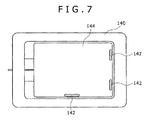
- FIG. 7 is a plan view of the case 140 showing the details of the through-holes.
- the case 140 has the housing part 144 formed of a recess having a rectangular shape at the position corresponding to the sensor substrate 110 and the sheet member 130. As shown in FIG. 2 , the depth of the housing part 144 is so designed that the surface position of the sheet member 130 is almost at the same level as that of the surface of the case 140 in the periphery of the housing part 144 when the sensor substrate 110 and the sheet member 130 are housed in the housing part 144.
- the through-holes 142 at three places are formed through the bottom of the housing part 144 and near the periphery of the housing part 144 (near the sidewall thereof). Each through-hole 142 is formed inside the sidewall of the housing part 144. Forming the through-hole 142 at such a position makes it possible to shield the entire through-hole 142 with the sheet member 130.
- the present invention is not limited to the above-described embodiment but various modifications can be made without departing from the scope of the present invention.
- the sensor substrate 110 and the magnetic flux detection substrate 120 are used in combination.
- the conductor 116 connected to a fixed potential is disposed at the position opposed to the wiring area 114 adjacent to the detection area 112 in which the detection electrodes 112A and 112B are formed.
- the capacitance of the wiring 113 does not change, and thus lowering of the position detection accuracy can be prevented.
Landscapes
- Engineering & Computer Science (AREA)
- General Engineering & Computer Science (AREA)
- Theoretical Computer Science (AREA)
- Physics & Mathematics (AREA)
- Human Computer Interaction (AREA)
- General Physics & Mathematics (AREA)
- Electromagnetism (AREA)
- Measurement Of Length, Angles, Or The Like Using Electric Or Magnetic Means (AREA)
- Position Input By Displaying (AREA)
Abstract
Description
- The present application claims priority of Japanese Patent Application No.
2009-218229, filed on September 21, 2009 - The present invention relates to a position detecting device configured to perform position detection based on a capacitance system.
- There has been known a position detecting device formed by fitting an input unit into an opening part of a case. This input unit is configured by superposing a first detector of a capacitance system on a second detector of an electromagnetic induction system (refer to, e.g., Japanese Patent Laid-open No.
2009-162538 FIGS. 1 to 11 ). In this position detecting device, the position indicated by a part of the human body (e.g., a finger) is detected by the first detector. Furthermore, by the second detector, the position indicated by a pen-type position indicator, including a built-in resonant circuit composed of a coil and a capacitor, is detected. - The position detecting device disclosed in patent document 1 has a structure in which the detectors are fitted into the opening part of the case. This results in that the first detector, closer to the surface, is exposed through the entire opening part. The first detector includes a detection area for detecting the position indicated by the human body. If wiring (wires) led out from this detection area is arranged in an area adjacent to the detection area, even the capacitance of the wiring changes also when the human body gets close to the wiring, which leads to lowering accuracy in position detection by the capacitance system.
- There is a need to provide a position detecting device that is free from lowering of the position detection accuracy that may be caused when wiring is arranged adjacent to the detection area.
- According to an aspect of the present invention, there is provided a position detecting device that detects a position indicated by a human body part. The position detecting device includes a sensor substrate having a detection area, in which a plurality of detection electrodes are formed, and a wiring area, in which wiring led out from the detection electrodes is formed. The position detecting device further includes a case configured to house the sensor substrate. The sensor substrate further includes a conductor, connected to a fixed potential, which is provided at a position opposed to (i.e., facing) the wiring area. Because the conductor connected to the fixed potential is disposed at the position opposed to the wiring area adjacent to the detection area, in which the detection electrodes are formed, the capacitance of the wiring included in the wiring area does not change even when a human body part is brought close to the wiring. Thus, lowering of the position detection accuracy can be prevented. In particular, by employing the ground potential as the above-described fixed potential, change in the capacitance of the wiring due to the approach of a human body part can be surely prevented.
- By forming the above-described sensor substrate by using a flexible substrate, the position detecting device having a small thickness can be easily realized by disposing the sensor substrate on the surface of the case. In addition, the above-described adverse effect (change in the capacitance of the wiring) attributed to the placement of the sensor substrate on the surface of the case can be prevented.
- The position detecting device may further include a magnetic flux detection substrate disposed at a position opposed to (i.e., facing) the above-described sensor substrate, on the side opposite from the side in which a human body part indicates a position. The magnetic flux detection substrate has at least one loop coil for detecting magnetic flux generated by a coil provided in a position indicator. The entire surface of the sensor substrate housed in the case can be used as the effective area of the position indicator.
- It is desirable that the above-described conductor has a shape that reduces the occurrence of an eddy current on the surface, preferably a shape having a slit extending from an outer edge of the conductor toward the inside of the conductor. This feature can prevent the occurrence of the eddy current on the surface of the conductor due to a magnetic field generated by the magnetic flux detection substrate or the position indicator, and thus can prevent lowering of the accuracy of position detection based on an electromagnetic induction system.
-
-
FIG. 1 is a plan view of a position detecting device according to one embodiment of the present invention; -
FIG. 2 is an enlarged sectional view taken along line II-II inFIG. 1 ; -
FIG. 3 is a diagram for explaining the operation of the position detecting device; -
FIG. 4 is a plan view showing a sensor substrate; -
FIG. 5 is a partial plan view showing part of the sensor substrate in an enlarged manner; -
FIG. 6 is a diagram showing a conductor provided at the position corresponding to an adjacent wiring area; -
FIG. 7 is a plan view of a case for showing the details of through-holes; and -
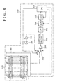
FIG. 8 is a block diagram for explaining position detection operation by use of a magnetic flux detection substrate. - A position detecting device according to one embodiment of the present invention will be described below with reference to the drawings.
-
FIG. 1 is a plan view of the position detecting device according to one embodiment.FIG. 2 is an enlarged sectional view taken along line II-II ofFIG. 1 . Theposition detecting device 100 of the present embodiment is configured to detect a position indicated by part of the human body (e.g. a fingertip) or a position indicator 200 (FIG. 3 ). Theposition detecting device 100 includes asensor substrate 110 serving as a first detector for performing position detection based on a capacitance system, and a magneticflux detection substrate 120 serving as a second detector for performing position detection based on an electromagnetic induction system. Theposition detecting device 100 further includes asheet member 130 covering the surface of thesensor substrate 110, acase 140 having ahousing part 144 for housing thesensor substrate 110, the magneticflux detection substrate 120, and thesheet member 130, and various types of circuits (FIG. 3 ) necessary for position detection. Theposition detecting device 100 is connected to an external apparatus (not shown), such as a personal computer or a personal digital assistant (PDA), and is used as an input device for the external apparatus. When a position on the surface of thesheet member 130 is indicated (pointed to) by a fingertip or theposition indicator 200, the coordinate data of this indicated position is output from theposition detecting device 100 to the external apparatus. In the example shown inFIG. 2 , gaps are provided among thesheet member 130, thesensor substrate 110, and thehousing part 144 for easy understanding. However, in practice, these components are bonded to each other by an adhesive, so as to ensure that they are in tight contact with each other evenly. -
FIG. 3 is a diagram for explaining the operation of theposition detecting device 100. As shown inFIG. 3 , theposition detecting device 100 includes acapacitance measuring unit 150, anelectromagnetic induction detector 152, and aprocessing circuit 154 as the various types of circuits for position detection. - The
capacitance measuring unit 150 is a circuit configured to measure a change in the capacitance of detection electrodes provided in thesensor substrate 110, and is connected to thesensor substrate 110 and theprocessing circuit 154. Theelectromagnetic induction detector 152 is a circuit configured to detect the position of the point indicated by aposition indicator 200 based on an electromagnetic induction system, and is connected to the magneticflux detection substrate 120 and theprocessing circuit 154. Theprocessing circuit 154 is a circuit configured to calculate the coordinate data of the point indicated by a fingertip or theposition indicator 200, which is detected by thesensor substrate 110 or the magneticflux detection substrate 120. The coordinate data calculated by theprocessing circuit 154 is sent to the external apparatus. - The details of the
sensor substrate 110 will be described below.FIG. 4 is a plan view showing the whole of thesensor substrate 110.FIG. 5 is a partial plan view showing part of thesensor substrate 110 in an enlarged manner. - The
sensor substrate 110 is a film substrate having flexibility, i.e. a flexible substrate. In the present embodiment, a polyethylene terephthalate (PET) substrate is used. A film substrate other than the PET substrate, such as a polyimide substrate, may be used. Thesensor substrate 110 includes adetection area 112, in whichplural detection electrodes wiring area 114, in whichwiring 113 led out from thedetection electrodes FIG. 6 ) disposed at the position opposed to (facing) thewiring area 114. - The
detection electrodes 112A each have a nearly-square shape, and are regularly arranged on the entire surface of thedetection area 112 in such a way that one diagonal of eachdetection electrode 112A is along the X direction (the direction along the longer sides of thedetection area 112 having a rectangular shape is defined as the X direction, and the direction along the shorter sides thereof is defined as the Y direction). Furthermore, thedetection electrodes 112A adjacent to each other along the X direction are electrically connected to each other via anauxiliary line 112C. Plural detection electrode groups, each composed of suchplural detection electrodes 112A connected to each other in one row along the X direction, are juxtaposed to each other along the Y direction. - Similarly, the
detection electrodes 112B each have a nearly-square shape as with thedetection electrode 112A, and are regularly arranged on the entire surface of thedetection area 112 in such a way that one diagonal of eachdetection electrode 112B is along the Y direction. Furthermore, thedetection electrodes 112B adjacent to each other along the Y direction are electrically connected to each other via anauxiliary line 112D. Plural detection electrode groups, each composed of suchplural detection electrodes 112B connected to each other in one row along the Y direction, are juxtaposed to each other along the X direction. - The
detection electrodes 112A and thedetection electrodes 112B are regularly arranged in thedetection area 112 in such a way that the gaps among thedetection electrodes 112A are filled by thedetection electrodes 112B and vice versa. When a fingertip of the user is brought into contact with the surface of thesheet member 130, the contact surface of the fingertip is opposed to both of thedetection electrode 112A and thedetection electrode 112B simultaneously. Although theauxiliary lines sensor substrate 110 having two, three or more metal layers, the electrical insulation between theauxiliary lines detection electrodes slits 112E (seeFIG. 5 ) are formed at positions along the other diagonal of each of thedetection electrodes flux detection substrate 120 or theposition indicator 200. The shape of theslits 112E shown inFIG. 5 is one example, and the shape and the number ofslits 112E can be changed according to each application. - The
capacitance measuring unit 150 detects change in the capacitance of the X-direction detection electrode group composed of theplural detection electrodes 112A, on a group-by-group basis, and detects change in the capacitance of the Y-direction detection electrode group composed of theplural detection electrodes 112B, also on a group-by-group basis. Theprocessing circuit 154 specifies the X-direction and Y-direction detection electrode groups whose capacitance is increased due to the approach of a fingertip, and calculates the position indicated by the fingertip. - The above-described
wiring area 114 includes anadjacent wiring area 114A, which is adjacent to the periphery of thedetection area 112 and includes thewiring 113 connected to thedetection electrodes lead wiring area 114B used for connecting thewiring 113 included in thisadjacent wiring area 114A to the processing circuit 154 (or the capacitance measuring unit 150). InFIG. 4 , thewiring area 114 is shown with hatched lines, and the direction of the hatched lines is different between theadjacent wiring area 114A and thelead wiring area 114B. - In the present embodiment, on the
sensor substrate 110, theconductor 116 connected to a fixed potential is provided on the surface side (on the side of the sheet member 130) and at the position opposed to (or facing) theadjacent wiring area 114A.FIG. 6 is a diagram showing theconductor 116 provided at the position corresponding to theadjacent wiring area 114A. As shown inFIG. 6 , theconductor 116 covers the whole of theadjacent wiring area 114A. - Detection by the above-described
capacitance measuring unit 150 is so performed that thedetection area 112 is the object of detection. However, even when theadjacent wiring area 114A is indicated (pointed to) by a fingertip of the user, the capacitance of thewiring 113 included in theadjacent wiring area 114A also changes. This possibly causes erroneous detection by thecapacitance measuring unit 150. Theconductor 116 is a component provided in order to prevent this erroneous detection. By covering thewiring 113 in theadjacent wiring area 114A with theconductor 116 connected to a fixed potential, the capacitance of thewiring 113 is prevented from changing even when a fingertip of the user gets close to theadjacent wiring area 114A. It is most preferable that the fixed potential connected to theconductor 116 be the ground potential. However, another potential may be employed in principle. Connection to the fixed potential is achieved via a line included in thelead wiring area 114B, for example. - The
conductor 116 has such a shape as to reduce the occurrence of eddy currents on the surface (the surface of theconductor 116 itself). Specifically, in theconductor 116,plural slits 116A extending from the outer edge of theconductor 116 toward the inside thereof are formed in order to reduce eddy currents arising due to magnetic flux generated by the magneticflux detection substrate 120 or theposition indicator 200. Any form other than theslits 116A shown inFIG. 6 may be employed as long as the form allows reduction of the occurrence of eddy currents. For example, many through-holes may be formed in theconductor 116, or many trenches (recesses and projections) may be formed on the surface of theconductor 116. - The area as the combination of the
detection area 112 and theadjacent wiring area 114A has a rectangular shape. Thelead wiring area 114B outwardly extends from one or plural places (in the example shown inFIG. 4 , three places) on the periphery of this rectangular shape. Furthermore, cutparts 114C having a concave shape are provided on the outer periphery of theadjacent wiring area 114A and adjacent to a respective one of thelead wiring areas 114B at two places. - The connection between the
sensor substrate 110 and thecapacitance measuring unit 150 is achieved by using thelead wiring area 114B. Specifically, part of the wiring area 114 (the root part of thelead wiring area 114B) is bent, and thelead wiring area 114B is deformed (bent) and routed in thecase 140. Thereby, the electrical connection between thesensor substrate 110 and thecapacitance measuring unit 150 is achieved. - For this purpose, in the
case 140, through-holes 142 are formed at three places corresponding to the positions through which thelead wiring areas 114B are routed.FIG. 7 is a plan view of thecase 140 showing the details of the through-holes. Thecase 140 has thehousing part 144 formed of a recess having a rectangular shape at the position corresponding to thesensor substrate 110 and thesheet member 130. As shown inFIG. 2 , the depth of thehousing part 144 is so designed that the surface position of thesheet member 130 is almost at the same level as that of the surface of thecase 140 in the periphery of thehousing part 144 when thesensor substrate 110 and thesheet member 130 are housed in thehousing part 144. The through-holes 142 at three places are formed through the bottom of thehousing part 144 and near the periphery of the housing part 144 (near the sidewall thereof). Each through-hole 142 is formed inside the sidewall of thehousing part 144. Forming the through-hole 142 at such a position makes it possible to shield the entire through-hole 142 with thesheet member 130. - The
lead wiring area 114B is bent from its root part and the bent part is made to pass through the through-hole 142 (seeFIG. 2 ), so that the end of thelead wiring area 114B is connected to thecapacitance measuring unit 150. - Position detection based on the magnetic
flux detection substrate 120 will be described below.FIG. 8 is a block diagram for explaining position detection operation based on the magneticflux detection substrate 120. The magneticflux detection substrate 120 is provided at a position opposed to (facing) thesensor substrate 110, either on the front surface or back surface of thecase 140. In the example ofFIG. 2 , the magneticflux detection substrate 120 is disposed on the back surface side of thecase 140. However, it may be disposed on the front surface side of thecase 140 in the area sandwiched between thecase 140 and thesensor substrate 110. - The magnetic
flux detection substrate 120 includes plural (e.g. 40) loop coils along each of the X direction and the Y direction (these X and Y directions are the same as those of the X and Y directions in thesensor substrate 110 shown inFIG. 4 ). - The
electromagnetic induction detector 152 includes aselection circuit 300, a transmission/reception switch circuit 302, anamplifier 304, adetector circuit 306, a low-pass filter (LPF) 308, a sample hold circuit (S/H) 310, an analog-digital converter (A/D) 312, aCPU 314, anoscillator 316, and adriver 318. Theselection circuit 300 selects one loop coil among the plural loop coils included in the magneticflux detection substrate 120 and connects it to the transmission/reception switch circuit 302. In the state in which the transmission/reception switch circuit 302 is switched to the transmission side (T), the loop coil selected by theselection circuit 300 is connected to thedriver 318. In this state, when an AC signal of a predetermined frequency is output from theoscillator 316, thedriver 318 makes a current flow to the connected loop coil, so that a magnetic field is generated by this loop coil. - The
position indicator 200 includes a built-in resonant circuit formed by connecting a coil and a capacitor in parallel. If theposition indicator 200 is brought close to the surface of theposition detecting device 100 in the state in which magnetic flux is generated by the loop coil, voltage induced in the coil in theposition indicator 200 is applied to the capacitor and a charge is accumulated therein. Thereafter, when the transmission/reception switch circuit 302 is switched to the reception side (R), the generation of the magnetic field by the loop coil is stopped. Then, the charge accumulated in the capacitor until then is discharged from theposition indicator 200 and a current flows through the coil, so that a magnetic field is generated by this coil. In this state, the intensity of the signal output from each loop coil is detected while switching the selected loop coil by theselection circuit 300. Thereby, the position of theposition indicator 200 is specified. Specifically, this signal intensity detection is carried out through the following process. For the signal amplified by theamplifier 304, detection processing (e.g. AM wave detection processing) is executed by thedetector circuit 306. Furthermore, the signal resulting from the passage through theLPF 308 is converted to digital data by using thesample hold circuit 310 and the analog-digital converter 312. The digital data is processed by theCPU 314. - As described above, the
position detecting device 100 of the present embodiment has theconductor 116 connected to a fixed potential at the position opposed to thewiring area 114 on thesensor substrate 110. Therefore, even when the human body is brought close to thewiring 113 included in thewiring area 114, the capacitance of thewiring 113 does not change, and thus lowering of the position detection accuracy can be prevented. In particular, by employing the ground potential as the above-described fixed potential, change in the capacitance due to the approach of a human body part can be surely prevented. - Furthermore, by forming the
sensor substrate 110 by using a flexible substrate, theposition detecting device 100 having a small thickness can be easily realized by disposing thesensor substrate 110 on the surface of the case. In addition, the above-described adverse effect (change in the capacitance of the wiring 113) attributed to the placement of thesensor substrate 110 on the surface of the case can be prevented. Moreover, in the case of using thesensor substrate 110 and the magneticflux detection substrate 120 in combination, the entire surface of thesensor substrate 110 housed in thecase 140 can be used as the effective area of theposition indicator 200. - Furthermore, by forming the
conductor 116 into such a shape as to reduce the occurrence of eddy currents on the surface, preferably a shape having theslits 116A extending from the outer edge of theconductor 116 toward the inside thereof, eddy currents can be prevented from arising on the surface of theconductor 116 due to a magnetic field generated by the magneticflux detection substrate 120 or theposition indicator 200. Thus, lowering of the accuracy of position detection by the electromagnetic induction system can be prevented. - It should be noted that the present invention is not limited to the above-described embodiment but various modifications can be made without departing from the scope of the present invention. For example, in the above-described embodiment, the
sensor substrate 110 and the magneticflux detection substrate 120 are used in combination. However, it is also possible to apply the present invention to a position detecting device including only thesensor substrate 110 of a capacitance system. - Furthermore, in the above-described embodiment, the
entire sensor substrate 110 is formed by using a film substrate having flexibility (flexible substrate). However, the material of the main body part composed of thedetection area 112 and theadjacent wiring area 114A in thesensor substrate 110 may be different from that of thelead wiring area 114B, and only thelead wiring area 114B may be formed by using a material having flexibility. Furthermore, the present invention can be applied also where theentire sensor substrate 110 is formed by using a material having no flexibility. - According to the embodiment of the present invention, the
conductor 116 connected to a fixed potential is disposed at the position opposed to thewiring area 114 adjacent to thedetection area 112 in which thedetection electrodes wiring 113 included in thewiring area 114, the capacitance of thewiring 113 does not change, and thus lowering of the position detection accuracy can be prevented.
Claims (6)
- A position detecting device comprising:a sensor substrate having a detection area, in which a plurality of detection electrodes are formed, and a wiring area, in which wiring led out from the detection electrodes is formed; anda case configured to house the sensor substrate, whereinthe sensor substrate further has a conductor connected to a fixed potential at a position opposed to the wiring area.
- The position detecting device according to claim 1, wherein
the fixed potential is a ground potential. - The position detecting device according to claims 1 or 2, further comprising:a magnetic flux detection substrate disposed at a position opposed to the sensor substrate on a side opposite from a side in which a human body indicates a position, the magnetic flux detection substrate having a loop coil for detecting magnetic flux generated by a coil provided in a position indicator.
- The position detecting device according to one of the preceding claims, wherein
the conductor has a shape that reduces occurrence of an eddy current on a conductor surface. - The position detecting device according to claim 4, wherein
the shape that reduces occurrence of an eddy current is a shape having a slit extending from an outer edge of the conductor toward inside of the conductor. - The position detecting device according to one of the preceding claims, wherein
the sensor substrate is a flexible substrate.
Applications Claiming Priority (1)
| Application Number | Priority Date | Filing Date | Title |
|---|---|---|---|
| JP2009218229A JP5466908B2 (en) | 2009-09-21 | 2009-09-21 | Sensor substrate and position detection device |
Publications (2)
| Publication Number | Publication Date |
|---|---|
| EP2333648A1 true EP2333648A1 (en) | 2011-06-15 |
| EP2333648B1 EP2333648B1 (en) | 2014-07-09 |
Family
ID=43413739
Family Applications (1)
| Application Number | Title | Priority Date | Filing Date |
|---|---|---|---|
| EP10175429.9A Not-in-force EP2333648B1 (en) | 2009-09-21 | 2010-09-06 | Position detecting device |
Country Status (5)
| Country | Link |
|---|---|
| US (1) | US8390272B2 (en) |
| EP (1) | EP2333648B1 (en) |
| JP (1) | JP5466908B2 (en) |
| CN (2) | CN102023771B (en) |
| TW (1) | TWI499956B (en) |
Cited By (1)
| Publication number | Priority date | Publication date | Assignee | Title |
|---|---|---|---|---|
| CN102866813A (en) * | 2011-07-08 | 2013-01-09 | 株式会社和冠 | Position detecting sensor, position detecting device, and position detecting method |
Families Citing this family (29)
| Publication number | Priority date | Publication date | Assignee | Title |
|---|---|---|---|---|
| BRPI1008199A2 (en) * | 2009-06-05 | 2016-03-01 | Koninkl Philips Electronics Nv | capacitive detection system for detecting an object, capacitive detection method for detecting an object and computer program for detecting an object |
| JP5430339B2 (en) | 2009-10-19 | 2014-02-26 | 株式会社ワコム | Position detecting device and position indicator |
| JP2012202254A (en) | 2011-03-24 | 2012-10-22 | Hitachi Automotive Systems Ltd | Pump device |
| CN102902393B (en) * | 2011-07-29 | 2015-11-25 | 宸鸿光电科技股份有限公司 | Detection electrode array control circuit, control method and touch detection system thereof |
| US8804347B2 (en) | 2011-09-09 | 2014-08-12 | Apple Inc. | Reducing the border area of a device |
| JP5871307B2 (en) * | 2011-09-30 | 2016-03-01 | 株式会社ワコム | Position detection sensor unit and position detection device |
| JP5348255B2 (en) * | 2012-01-11 | 2013-11-20 | 大日本印刷株式会社 | Touch panel sensor and touch panel sensor with flexible printed wiring board |
| JP6040527B2 (en) * | 2012-01-16 | 2016-12-07 | 大日本印刷株式会社 | Touch panel sensor and touch panel sensor with flexible printed wiring board |
| KR20140033785A (en) * | 2012-09-10 | 2014-03-19 | 삼성전기주식회사 | Digitizer |
| TWD158449S (en) * | 2012-12-17 | 2014-01-11 | 和冠股份有限公司 | Coordinate input machine |
| TWD160088S (en) * | 2013-04-04 | 2014-04-21 | 和冠股份有限公司 | Coordinate input device |
| CN103295671B (en) * | 2013-05-30 | 2016-08-10 | 南昌欧菲光科技有限公司 | Nesa coating |
| CN103294272B (en) * | 2013-05-30 | 2016-04-13 | 南昌欧菲光科技有限公司 | Nesa coating |
| CN103295670B (en) * | 2013-05-30 | 2015-11-25 | 南昌欧菲光科技有限公司 | Nesa coating |
| CN103345961A (en) * | 2013-05-30 | 2013-10-09 | 南昌欧菲光科技有限公司 | Transparent conducting film |
| JP6103533B2 (en) * | 2013-06-12 | 2017-03-29 | アルプス電気株式会社 | Input device |
| CN103425341B (en) * | 2013-07-30 | 2016-10-26 | 南昌欧菲光科技有限公司 | One-layer multi-point touch control screen and one-layer multi-point conducting film thereof |
| CN103426503A (en) * | 2013-07-30 | 2013-12-04 | 南昌欧菲光科技有限公司 | Monolayer multiple-point touch screen and monolayer multiple-point conductive film thereof |
| CN103425340B (en) * | 2013-07-30 | 2017-11-21 | 南昌欧菲光科技有限公司 | One-layer multi-point touch control screen and its one-layer multi-point conducting film |
| CN103455198B (en) * | 2013-07-30 | 2016-12-28 | 南昌欧菲光科技有限公司 | One-layer multi-point touch control screen and one-layer multi-point conducting film thereof |
| CN104347154B (en) * | 2013-07-31 | 2017-11-03 | 南昌欧菲光科技有限公司 | A transparent conductive film |
| KR102037515B1 (en) | 2013-08-29 | 2019-10-28 | 엘지디스플레이 주식회사 | Electrostatic capacitive type touch-sensitive panel for display device |
| KR102125404B1 (en) | 2013-10-15 | 2020-06-22 | 엘지디스플레이 주식회사 | Touch sensing system and diplay device |
| KR102193915B1 (en) * | 2014-02-10 | 2020-12-23 | 삼성디스플레이 주식회사 | Touch sensor substrate and display apparatus having the touch sensor substrate |
| KR102183097B1 (en) * | 2014-03-10 | 2020-11-25 | 엘지전자 주식회사 | Conductive film and touch panel including the same |
| CN106155403B (en) * | 2015-04-27 | 2023-05-02 | 安徽精卓光显技术有限责任公司 | Touch control element |
| WO2016186191A1 (en) | 2015-05-21 | 2016-11-24 | 株式会社ワコム | Active stylus |
| JP1576209S (en) * | 2016-12-21 | 2017-05-15 | ||
| US20220390642A1 (en) * | 2021-06-02 | 2022-12-08 | Nwave Technologies Inc | Battery-powered vehicle detecting device using an embedded inductive sensor |
Citations (3)
| Publication number | Priority date | Publication date | Assignee | Title |
|---|---|---|---|---|
| US20060066581A1 (en) * | 2004-09-24 | 2006-03-30 | Apple Computer, Inc. | Low EMI capacitive trackpad |
| WO2006130749A1 (en) * | 2005-06-01 | 2006-12-07 | Synaptics Incorporated | Touch pad with flexible substrate |
| EP2077489A1 (en) * | 2007-12-28 | 2009-07-08 | Wacom Co., Ltd. | Position detecting device |
Family Cites Families (17)
| Publication number | Priority date | Publication date | Assignee | Title |
|---|---|---|---|---|
| JPS6370326A (en) * | 1986-09-12 | 1988-03-30 | Wacom Co Ltd | Position detector |
| US5913820A (en) * | 1992-08-14 | 1999-06-22 | British Telecommunications Public Limited Company | Position location system |
| JPH07295724A (en) * | 1994-04-22 | 1995-11-10 | Seiko Epson Corp | Tablet |
| US5752513A (en) * | 1995-06-07 | 1998-05-19 | Biosense, Inc. | Method and apparatus for determining position of object |
| JP3426847B2 (en) * | 1996-05-14 | 2003-07-14 | アルプス電気株式会社 | Coordinate input device |
| US7800592B2 (en) | 2005-03-04 | 2010-09-21 | Apple Inc. | Hand held electronic device with multiple touch sensing devices |
| KR100459230B1 (en) | 2002-11-14 | 2004-12-03 | 엘지.필립스 엘시디 주식회사 | touch panel for display device |
| JP4271475B2 (en) * | 2003-03-31 | 2009-06-03 | 株式会社ワコー | Force detection device |
| JP4435622B2 (en) * | 2004-05-25 | 2010-03-24 | アルプス電気株式会社 | Capacitance type detection device |
| WO2007129085A2 (en) * | 2006-05-09 | 2007-11-15 | Sensopad Limited | Navigation arrangement for an electronic device |
| JP4915232B2 (en) * | 2006-12-19 | 2012-04-11 | ソニー株式会社 | Coordinate input device and coordinate input system |
| TW200844811A (en) * | 2007-03-27 | 2008-11-16 | N trig ltd | Shield for a digitizer sensor |
| JP2008257374A (en) * | 2007-04-03 | 2008-10-23 | Sharp Corp | Mobile information terminal and mobile phone |
| JP4554651B2 (en) * | 2007-08-01 | 2010-09-29 | ホシデン株式会社 | Touch panel input device |
| TW200921483A (en) * | 2007-11-09 | 2009-05-16 | Tpk Touch Solutions Inc | Touch-control display panel with an electric-field shielding layer |
| TWI355104B (en) * | 2007-12-21 | 2011-12-21 | Hon Hai Prec Ind Co Ltd | Touch panel and displaying device using the same |
| JP5439068B2 (en) * | 2009-07-08 | 2014-03-12 | 株式会社ワコー | Force detection device |
-
2009
- 2009-09-21 JP JP2009218229A patent/JP5466908B2/en active Active
-
2010
- 2010-07-22 US US12/841,893 patent/US8390272B2/en active Active
- 2010-08-18 TW TW099127576A patent/TWI499956B/en not_active IP Right Cessation
- 2010-09-06 EP EP10175429.9A patent/EP2333648B1/en not_active Not-in-force
- 2010-09-07 CN CN201010275791.0A patent/CN102023771B/en active Active
- 2010-09-07 CN CN2010205211701U patent/CN201765581U/en not_active Expired - Lifetime
Patent Citations (4)
| Publication number | Priority date | Publication date | Assignee | Title |
|---|---|---|---|---|
| US20060066581A1 (en) * | 2004-09-24 | 2006-03-30 | Apple Computer, Inc. | Low EMI capacitive trackpad |
| WO2006130749A1 (en) * | 2005-06-01 | 2006-12-07 | Synaptics Incorporated | Touch pad with flexible substrate |
| EP2077489A1 (en) * | 2007-12-28 | 2009-07-08 | Wacom Co., Ltd. | Position detecting device |
| JP2009162538A (en) | 2007-12-28 | 2009-07-23 | Wacom Co Ltd | Position detection device |
Cited By (1)
| Publication number | Priority date | Publication date | Assignee | Title |
|---|---|---|---|---|
| CN102866813A (en) * | 2011-07-08 | 2013-01-09 | 株式会社和冠 | Position detecting sensor, position detecting device, and position detecting method |
Also Published As
| Publication number | Publication date |
|---|---|
| US8390272B2 (en) | 2013-03-05 |
| US20110068776A1 (en) | 2011-03-24 |
| JP5466908B2 (en) | 2014-04-09 |
| TWI499956B (en) | 2015-09-11 |
| JP2011065614A (en) | 2011-03-31 |
| CN102023771A (en) | 2011-04-20 |
| CN201765581U (en) | 2011-03-16 |
| EP2333648B1 (en) | 2014-07-09 |
| CN102023771B (en) | 2015-04-01 |
| TW201112096A (en) | 2011-04-01 |
Similar Documents
| Publication | Publication Date | Title |
|---|---|---|
| US8390272B2 (en) | Position detecting device | |
| JP5886489B2 (en) | Position detection device | |
| KR101911842B1 (en) | Printed Circuit Board Comprising an Electrode Configuration of a Capacitive Sensor | |
| JP5866583B2 (en) | Current sensor | |
| US7397233B2 (en) | Voltage measuring device | |
| EP3161962B1 (en) | Compensation of a target object's coupling to feeding lines in capacitive sensing system | |
| KR20170104985A (en) | Electrode arrangement for gesture detection and tracking | |
| JP6747257B2 (en) | Control device | |
| KR20180017000A (en) | Sensor structure for improved touch and gesture decoding | |
| JP2019191143A (en) | Electrostatic capacitance sensor, electrostatic capacitance sensor head, and location detection system | |
| JP2011060037A (en) | Position detector and electrostatic sensor | |
| US10768021B2 (en) | Position detection device and position detection method | |
| US7277817B2 (en) | Position sensing device | |
| JPH03204716A (en) | Tablet for coordinate detector | |
| JP2013105650A (en) | Semiconductor device and electronic device with the same | |
| US20240302924A1 (en) | Capacitance measurement circuit module |
Legal Events
| Date | Code | Title | Description |
|---|---|---|---|
| PUAI | Public reference made under article 153(3) epc to a published international application that has entered the european phase |
Free format text: ORIGINAL CODE: 0009012 |
|
| AK | Designated contracting states |
Kind code of ref document: A1 Designated state(s): AL AT BE BG CH CY CZ DE DK EE ES FI FR GB GR HR HU IE IS IT LI LT LU LV MC MK MT NL NO PL PT RO SE SI SK SM TR |
|
| AX | Request for extension of the european patent |
Extension state: BA ME RS |
|
| 17P | Request for examination filed |
Effective date: 20111214 |
|
| 17Q | First examination report despatched |
Effective date: 20120423 |
|
| GRAP | Despatch of communication of intention to grant a patent |
Free format text: ORIGINAL CODE: EPIDOSNIGR1 |
|
| INTG | Intention to grant announced |
Effective date: 20140212 |
|
| GRAS | Grant fee paid |
Free format text: ORIGINAL CODE: EPIDOSNIGR3 |
|
| GRAA | (expected) grant |
Free format text: ORIGINAL CODE: 0009210 |
|
| AK | Designated contracting states |
Kind code of ref document: B1 Designated state(s): AL AT BE BG CH CY CZ DE DK EE ES FI FR GB GR HR HU IE IS IT LI LT LU LV MC MK MT NL NO PL PT RO SE SI SK SM TR |
|
| REG | Reference to a national code |
Ref country code: GB Ref legal event code: FG4D |
|
| RIN1 | Information on inventor provided before grant (corrected) |
Inventor name: MUNAKATA, HIROSHI Inventor name: YOKOTA, MASARU |
|
| REG | Reference to a national code |
Ref country code: CH Ref legal event code: EP Ref country code: AT Ref legal event code: REF Ref document number: 676794 Country of ref document: AT Kind code of ref document: T Effective date: 20140715 |
|
| REG | Reference to a national code |
Ref country code: IE Ref legal event code: FG4D |
|
| REG | Reference to a national code |
Ref country code: DE Ref legal event code: R096 Ref document number: 602010017323 Country of ref document: DE Effective date: 20140821 |
|
| REG | Reference to a national code |
Ref country code: AT Ref legal event code: MK05 Ref document number: 676794 Country of ref document: AT Kind code of ref document: T Effective date: 20140709 |
|
| REG | Reference to a national code |
Ref country code: NL Ref legal event code: VDEP Effective date: 20140709 |
|
| REG | Reference to a national code |
Ref country code: LT Ref legal event code: MG4D |
|
| PG25 | Lapsed in a contracting state [announced via postgrant information from national office to epo] |
Ref country code: GR Free format text: LAPSE BECAUSE OF FAILURE TO SUBMIT A TRANSLATION OF THE DESCRIPTION OR TO PAY THE FEE WITHIN THE PRESCRIBED TIME-LIMIT Effective date: 20141010 Ref country code: BG Free format text: LAPSE BECAUSE OF FAILURE TO SUBMIT A TRANSLATION OF THE DESCRIPTION OR TO PAY THE FEE WITHIN THE PRESCRIBED TIME-LIMIT Effective date: 20141009 Ref country code: PT Free format text: LAPSE BECAUSE OF FAILURE TO SUBMIT A TRANSLATION OF THE DESCRIPTION OR TO PAY THE FEE WITHIN THE PRESCRIBED TIME-LIMIT Effective date: 20141110 Ref country code: ES Free format text: LAPSE BECAUSE OF FAILURE TO SUBMIT A TRANSLATION OF THE DESCRIPTION OR TO PAY THE FEE WITHIN THE PRESCRIBED TIME-LIMIT Effective date: 20140709 Ref country code: LT Free format text: LAPSE BECAUSE OF FAILURE TO SUBMIT A TRANSLATION OF THE DESCRIPTION OR TO PAY THE FEE WITHIN THE PRESCRIBED TIME-LIMIT Effective date: 20140709 Ref country code: SE Free format text: LAPSE BECAUSE OF FAILURE TO SUBMIT A TRANSLATION OF THE DESCRIPTION OR TO PAY THE FEE WITHIN THE PRESCRIBED TIME-LIMIT Effective date: 20140709 Ref country code: FI Free format text: LAPSE BECAUSE OF FAILURE TO SUBMIT A TRANSLATION OF THE DESCRIPTION OR TO PAY THE FEE WITHIN THE PRESCRIBED TIME-LIMIT Effective date: 20140709 Ref country code: NO Free format text: LAPSE BECAUSE OF FAILURE TO SUBMIT A TRANSLATION OF THE DESCRIPTION OR TO PAY THE FEE WITHIN THE PRESCRIBED TIME-LIMIT Effective date: 20141009 |
|
| PG25 | Lapsed in a contracting state [announced via postgrant information from national office to epo] |
Ref country code: PL Free format text: LAPSE BECAUSE OF FAILURE TO SUBMIT A TRANSLATION OF THE DESCRIPTION OR TO PAY THE FEE WITHIN THE PRESCRIBED TIME-LIMIT Effective date: 20140709 Ref country code: CY Free format text: LAPSE BECAUSE OF FAILURE TO SUBMIT A TRANSLATION OF THE DESCRIPTION OR TO PAY THE FEE WITHIN THE PRESCRIBED TIME-LIMIT Effective date: 20140709 Ref country code: IS Free format text: LAPSE BECAUSE OF FAILURE TO SUBMIT A TRANSLATION OF THE DESCRIPTION OR TO PAY THE FEE WITHIN THE PRESCRIBED TIME-LIMIT Effective date: 20141109 Ref country code: LV Free format text: LAPSE BECAUSE OF FAILURE TO SUBMIT A TRANSLATION OF THE DESCRIPTION OR TO PAY THE FEE WITHIN THE PRESCRIBED TIME-LIMIT Effective date: 20140709 Ref country code: NL Free format text: LAPSE BECAUSE OF FAILURE TO SUBMIT A TRANSLATION OF THE DESCRIPTION OR TO PAY THE FEE WITHIN THE PRESCRIBED TIME-LIMIT Effective date: 20140709 Ref country code: HR Free format text: LAPSE BECAUSE OF FAILURE TO SUBMIT A TRANSLATION OF THE DESCRIPTION OR TO PAY THE FEE WITHIN THE PRESCRIBED TIME-LIMIT Effective date: 20140709 Ref country code: AT Free format text: LAPSE BECAUSE OF FAILURE TO SUBMIT A TRANSLATION OF THE DESCRIPTION OR TO PAY THE FEE WITHIN THE PRESCRIBED TIME-LIMIT Effective date: 20140709 |
|
| REG | Reference to a national code |
Ref country code: DE Ref legal event code: R097 Ref document number: 602010017323 Country of ref document: DE |
|
| PG25 | Lapsed in a contracting state [announced via postgrant information from national office to epo] |
Ref country code: DK Free format text: LAPSE BECAUSE OF FAILURE TO SUBMIT A TRANSLATION OF THE DESCRIPTION OR TO PAY THE FEE WITHIN THE PRESCRIBED TIME-LIMIT Effective date: 20140709 Ref country code: EE Free format text: LAPSE BECAUSE OF FAILURE TO SUBMIT A TRANSLATION OF THE DESCRIPTION OR TO PAY THE FEE WITHIN THE PRESCRIBED TIME-LIMIT Effective date: 20140709 Ref country code: MC Free format text: LAPSE BECAUSE OF FAILURE TO SUBMIT A TRANSLATION OF THE DESCRIPTION OR TO PAY THE FEE WITHIN THE PRESCRIBED TIME-LIMIT Effective date: 20140709 Ref country code: CZ Free format text: LAPSE BECAUSE OF FAILURE TO SUBMIT A TRANSLATION OF THE DESCRIPTION OR TO PAY THE FEE WITHIN THE PRESCRIBED TIME-LIMIT Effective date: 20140709 Ref country code: RO Free format text: LAPSE BECAUSE OF FAILURE TO SUBMIT A TRANSLATION OF THE DESCRIPTION OR TO PAY THE FEE WITHIN THE PRESCRIBED TIME-LIMIT Effective date: 20140709 Ref country code: LU Free format text: LAPSE BECAUSE OF FAILURE TO SUBMIT A TRANSLATION OF THE DESCRIPTION OR TO PAY THE FEE WITHIN THE PRESCRIBED TIME-LIMIT Effective date: 20140906 Ref country code: IT Free format text: LAPSE BECAUSE OF FAILURE TO SUBMIT A TRANSLATION OF THE DESCRIPTION OR TO PAY THE FEE WITHIN THE PRESCRIBED TIME-LIMIT Effective date: 20140709 Ref country code: SK Free format text: LAPSE BECAUSE OF FAILURE TO SUBMIT A TRANSLATION OF THE DESCRIPTION OR TO PAY THE FEE WITHIN THE PRESCRIBED TIME-LIMIT Effective date: 20140709 |
|
| REG | Reference to a national code |
Ref country code: CH Ref legal event code: PL |
|
| PLBE | No opposition filed within time limit |
Free format text: ORIGINAL CODE: 0009261 |
|
| STAA | Information on the status of an ep patent application or granted ep patent |
Free format text: STATUS: NO OPPOSITION FILED WITHIN TIME LIMIT |
|
| 26N | No opposition filed |
Effective date: 20150410 |
|
| REG | Reference to a national code |
Ref country code: IE Ref legal event code: MM4A |
|
| REG | Reference to a national code |
Ref country code: FR Ref legal event code: ST Effective date: 20150529 |
|
| PG25 | Lapsed in a contracting state [announced via postgrant information from national office to epo] |
Ref country code: BE Free format text: LAPSE BECAUSE OF NON-PAYMENT OF DUE FEES Effective date: 20140930 |
|
| PG25 | Lapsed in a contracting state [announced via postgrant information from national office to epo] |
Ref country code: CH Free format text: LAPSE BECAUSE OF NON-PAYMENT OF DUE FEES Effective date: 20140930 Ref country code: LI Free format text: LAPSE BECAUSE OF NON-PAYMENT OF DUE FEES Effective date: 20140930 |
|
| PG25 | Lapsed in a contracting state [announced via postgrant information from national office to epo] |
Ref country code: IE Free format text: LAPSE BECAUSE OF NON-PAYMENT OF DUE FEES Effective date: 20140906 Ref country code: FR Free format text: LAPSE BECAUSE OF NON-PAYMENT OF DUE FEES Effective date: 20140930 |
|
| PG25 | Lapsed in a contracting state [announced via postgrant information from national office to epo] |
Ref country code: SI Free format text: LAPSE BECAUSE OF FAILURE TO SUBMIT A TRANSLATION OF THE DESCRIPTION OR TO PAY THE FEE WITHIN THE PRESCRIBED TIME-LIMIT Effective date: 20140709 |
|
| PG25 | Lapsed in a contracting state [announced via postgrant information from national office to epo] |
Ref country code: SM Free format text: LAPSE BECAUSE OF FAILURE TO SUBMIT A TRANSLATION OF THE DESCRIPTION OR TO PAY THE FEE WITHIN THE PRESCRIBED TIME-LIMIT Effective date: 20140709 |
|
| PG25 | Lapsed in a contracting state [announced via postgrant information from national office to epo] |
Ref country code: MT Free format text: LAPSE BECAUSE OF FAILURE TO SUBMIT A TRANSLATION OF THE DESCRIPTION OR TO PAY THE FEE WITHIN THE PRESCRIBED TIME-LIMIT Effective date: 20140709 |
|
| PG25 | Lapsed in a contracting state [announced via postgrant information from national office to epo] |
Ref country code: TR Free format text: LAPSE BECAUSE OF FAILURE TO SUBMIT A TRANSLATION OF THE DESCRIPTION OR TO PAY THE FEE WITHIN THE PRESCRIBED TIME-LIMIT Effective date: 20140709 Ref country code: BE Free format text: LAPSE BECAUSE OF FAILURE TO SUBMIT A TRANSLATION OF THE DESCRIPTION OR TO PAY THE FEE WITHIN THE PRESCRIBED TIME-LIMIT Effective date: 20140709 Ref country code: HU Free format text: LAPSE BECAUSE OF FAILURE TO SUBMIT A TRANSLATION OF THE DESCRIPTION OR TO PAY THE FEE WITHIN THE PRESCRIBED TIME-LIMIT; INVALID AB INITIO Effective date: 20100906 |
|
| PG25 | Lapsed in a contracting state [announced via postgrant information from national office to epo] |
Ref country code: MK Free format text: LAPSE BECAUSE OF FAILURE TO SUBMIT A TRANSLATION OF THE DESCRIPTION OR TO PAY THE FEE WITHIN THE PRESCRIBED TIME-LIMIT Effective date: 20140709 |
|
| PG25 | Lapsed in a contracting state [announced via postgrant information from national office to epo] |
Ref country code: AL Free format text: LAPSE BECAUSE OF FAILURE TO SUBMIT A TRANSLATION OF THE DESCRIPTION OR TO PAY THE FEE WITHIN THE PRESCRIBED TIME-LIMIT Effective date: 20140709 |
|
| PGFP | Annual fee paid to national office [announced via postgrant information from national office to epo] |
Ref country code: GB Payment date: 20220920 Year of fee payment: 13 Ref country code: DE Payment date: 20220620 Year of fee payment: 13 |
|
| REG | Reference to a national code |
Ref country code: DE Ref legal event code: R119 Ref document number: 602010017323 Country of ref document: DE |
|
| GBPC | Gb: european patent ceased through non-payment of renewal fee |
Effective date: 20230906 |
|
| PG25 | Lapsed in a contracting state [announced via postgrant information from national office to epo] |
Ref country code: GB Free format text: LAPSE BECAUSE OF NON-PAYMENT OF DUE FEES Effective date: 20230906 |
|
| PG25 | Lapsed in a contracting state [announced via postgrant information from national office to epo] |
Ref country code: GB Free format text: LAPSE BECAUSE OF NON-PAYMENT OF DUE FEES Effective date: 20230906 Ref country code: DE Free format text: LAPSE BECAUSE OF NON-PAYMENT OF DUE FEES Effective date: 20240403 |