WO2016186191A1 - Active stylus - Google Patents
Active stylus Download PDFInfo
- Publication number
- WO2016186191A1 WO2016186191A1 PCT/JP2016/064965 JP2016064965W WO2016186191A1 WO 2016186191 A1 WO2016186191 A1 WO 2016186191A1 JP 2016064965 W JP2016064965 W JP 2016064965W WO 2016186191 A1 WO2016186191 A1 WO 2016186191A1
- Authority
- WO
- WIPO (PCT)
- Prior art keywords
- signal
- mode
- unit
- switch
- stylus
- Prior art date
Links
Images


Classifications
-
- G—PHYSICS
- G06—COMPUTING; CALCULATING OR COUNTING
- G06F—ELECTRIC DIGITAL DATA PROCESSING
- G06F3/00—Input arrangements for transferring data to be processed into a form capable of being handled by the computer; Output arrangements for transferring data from processing unit to output unit, e.g. interface arrangements
- G06F3/01—Input arrangements or combined input and output arrangements for interaction between user and computer
- G06F3/03—Arrangements for converting the position or the displacement of a member into a coded form
- G06F3/033—Pointing devices displaced or positioned by the user, e.g. mice, trackballs, pens or joysticks; Accessories therefor
- G06F3/038—Control and interface arrangements therefor, e.g. drivers or device-embedded control circuitry
- G06F3/0383—Signal control means within the pointing device
-
- G—PHYSICS
- G06—COMPUTING; CALCULATING OR COUNTING
- G06F—ELECTRIC DIGITAL DATA PROCESSING
- G06F3/00—Input arrangements for transferring data to be processed into a form capable of being handled by the computer; Output arrangements for transferring data from processing unit to output unit, e.g. interface arrangements
- G06F3/01—Input arrangements or combined input and output arrangements for interaction between user and computer
- G06F3/03—Arrangements for converting the position or the displacement of a member into a coded form
- G06F3/033—Pointing devices displaced or positioned by the user, e.g. mice, trackballs, pens or joysticks; Accessories therefor
- G06F3/0354—Pointing devices displaced or positioned by the user, e.g. mice, trackballs, pens or joysticks; Accessories therefor with detection of 2D relative movements between the device, or an operating part thereof, and a plane or surface, e.g. 2D mice, trackballs, pens or pucks
- G06F3/03545—Pens or stylus
-
- G—PHYSICS
- G06—COMPUTING; CALCULATING OR COUNTING
- G06F—ELECTRIC DIGITAL DATA PROCESSING
- G06F3/00—Input arrangements for transferring data to be processed into a form capable of being handled by the computer; Output arrangements for transferring data from processing unit to output unit, e.g. interface arrangements
- G06F3/01—Input arrangements or combined input and output arrangements for interaction between user and computer
- G06F3/03—Arrangements for converting the position or the displacement of a member into a coded form
- G06F3/041—Digitisers, e.g. for touch screens or touch pads, characterised by the transducing means
- G06F3/0416—Control or interface arrangements specially adapted for digitisers
- G06F3/04162—Control or interface arrangements specially adapted for digitisers for exchanging data with external devices, e.g. smart pens, via the digitiser sensing hardware
-
- G—PHYSICS
- G06—COMPUTING; CALCULATING OR COUNTING
- G06F—ELECTRIC DIGITAL DATA PROCESSING
- G06F3/00—Input arrangements for transferring data to be processed into a form capable of being handled by the computer; Output arrangements for transferring data from processing unit to output unit, e.g. interface arrangements
- G06F3/01—Input arrangements or combined input and output arrangements for interaction between user and computer
- G06F3/03—Arrangements for converting the position or the displacement of a member into a coded form
- G06F3/041—Digitisers, e.g. for touch screens or touch pads, characterised by the transducing means
- G06F3/044—Digitisers, e.g. for touch screens or touch pads, characterised by the transducing means by capacitive means
- G06F3/0441—Digitisers, e.g. for touch screens or touch pads, characterised by the transducing means by capacitive means using active external devices, e.g. active pens, for receiving changes in electrical potential transmitted by the digitiser, e.g. tablet driving signals
-
- G—PHYSICS
- G06—COMPUTING; CALCULATING OR COUNTING
- G06F—ELECTRIC DIGITAL DATA PROCESSING
- G06F3/00—Input arrangements for transferring data to be processed into a form capable of being handled by the computer; Output arrangements for transferring data from processing unit to output unit, e.g. interface arrangements
- G06F3/01—Input arrangements or combined input and output arrangements for interaction between user and computer
- G06F3/03—Arrangements for converting the position or the displacement of a member into a coded form
- G06F3/041—Digitisers, e.g. for touch screens or touch pads, characterised by the transducing means
- G06F3/044—Digitisers, e.g. for touch screens or touch pads, characterised by the transducing means by capacitive means
- G06F3/0442—Digitisers, e.g. for touch screens or touch pads, characterised by the transducing means by capacitive means using active external devices, e.g. active pens, for transmitting changes in electrical potential to be received by the digitiser
Definitions
- the present invention relates to an active stylus, and more particularly to an active stylus that supports a plurality of systems.
- a stylus used in this type of position detection system is called an “active stylus” and is configured to transmit a signal to a sensor controller in the position detection device by electrostatic coupling with the electrode.
- the sensor controller detects the presence and position of the stylus by detecting this signal.
- Patent Document 1 as an example of such an active stylus, a position signal used exclusively for deriving coordinate data and a data signal representing information such as a pen pressure value and a unique ID of the stylus are provided to a sensor controller.
- a stylus configured to transmit to is disclosed.
- Patent Document 2 discloses another example of an active stylus.
- the stylus according to this example digitally transmits the result of detecting the pen pressure.
- a position detection device is configured by a display device and a transparent sensor, and the position detection device detects both an indication position and writing pressure by a stylus and a touch position by a finger by the transparent sensor. .
- first method a method using a signal obtained by modulating a pulse train signal (including a pulse signal and a rectangular wave signal)
- second method a method using a modulated signal
- Patent Document 3 discloses an example of a position detection system that conforms to the first method.
- the stylus according to this example includes a writing pressure detection unit that optically detects writing pressure and a signal transmission unit.
- the signal transmitted by the signal transmission unit includes a position signal pulse 910 used for detecting the position of the stylus by the position detection device, and the writing pressure detected by the writing pressure detection unit.
- a pressure signal pulse 950 indicating the level of.
- the position signal pulse 910 is transmitted intermittently, and the pressure signal pulse 950 is transmitted between transmissions of the position signal pulse 910 only when the pen pressure is detected (not in the hover operation state).
- the position signal pulse 910 is constituted by an AC pulse having a predetermined frequency (specifically, 28.125 Hz), and the pressure signal pulse 950 is constituted by a frequency-modulated pulse signal.
- Patent Document 4 also discloses an example of a position detection system that conforms to the first method.
- the stylus according to this example includes a TX drive circuit 680 as shown in FIG. 9 of Patent Document 4, thereby transmitting a TX signal 677 that is a pulse train signal similar to the TX signal 632 used at the time of finger detection. It is configured as follows.
- the TX signal 677 is detected by the controller via the coupling capacitance between the stylus and the sensor.
- Patent Document 4 also discloses a boosting mechanism when the stylus transmits a signal (paragraph [0084]). According to this, a booster 870 is provided on the stylus in order to allow the chip drive circuit 890 responsible for transmitting the TX signal 835 to amplify the TX signal 835.
- the position detection systems disclosed in Patent Documents 1 and 2 comply with the second method.
- the stylus according to the second method modulates a sine wave signal according to the writing pressure level, not a pulse train signal such as a signal used when detecting a finger (a signal transmitted from the sensor controller to the transmitting electrode in the sensor). Configured to transmit. Specifically, for example, a carrier signal of several hundred to several MHz is modulated by ASK or OOK and transmitted.
- the sensor controller receives the signal through the bandpass filter to extract the signal having the above frequency, and restores the writing pressure value.
- a position detection device corresponding only to the second method cannot receive a transmission signal of a stylus corresponding to only the first method, and a position detection device corresponding to only the first method is a stylus corresponding to only the second method.
- the transmission signal cannot be received.
- the stylus is changed every time the position detection device is moved. It was inconvenient because it was necessary.
- the transmission signal generated by the first method (for example, a signal obtained by modulating a pulse train signal) and the transmission signal generated by the second method (for example, a signal obtained by modulating a sine wave signal) ) May be alternately transmitted.
- the method of configuring the stylus in this way is referred to as “alternate transmission method”.
- the position detection device can receive the stylus transmission signal in both the position detection device corresponding to only the first method and the position detection device corresponding to only the second method. You don't have to change your stylus every time you move. However, since it is usually not possible to use both position detecting devices at once, in this method, one of the signals is always transmitted in vain. This is not a preferable state from the viewpoint of reducing the power consumption of the stylus.
- one of the objects of the present invention is that when a position detecting device corresponding to only the first method and a position detecting device corresponding to only the second method are used side by side, the power consumption is lower than that of the alternating transmission method.
- An object of the present invention is to provide an active stylus that can avoid having to change the stylus every time the position detecting device is moved.
- An active stylus is an active stylus that transmits information to a sensor controller in association with a change in an electric field via a coupling capacitance formed between the sensor and a core that forms a pen tip;
- An electrode provided in the vicinity of the core body, a writing pressure detection unit that detects a writing pressure level corresponding to the writing pressure applied to the core body, a power source, and a first power and a power supplied from the power source.
- the first transmission signal obtained by modulating the pulse train signal by the writing pressure level is supplied to the electrode during the operation in the first mode, Determining whether it is necessary to switch to the second mode, and supplying a second transmission signal obtained by modulating a sine wave signal by the writing pressure level to the electrode during the operation in the second mode,
- the first module When it is determined whether or not it is necessary to switch to the second mode, and it is determined that switching to the second mode is necessary, the operation is switched to the operation in the second mode, and the switching to the first mode is necessary.
- An active stylus comprising a signal processing unit that switches to the operation in the first mode when it is determined that there is.
- An active stylus is an active stylus that transmits information to a sensor controller in association with a change in an electric field via a coupling capacitance formed between the sensor and a pen tip.
- One of the first mode and the second mode is operated by the applied power, and the first transmission signal in which the pulse train is modulated by the writing pressure level is supplied to the electrode during the operation in the first mode.
- the pulse train While supplying to the electrode a second transmission signal generated by a modulation method different from the modulation method to be modulated, it is necessary to determine whether or not to switch to the first mode and to switch to the second mode.
- a signal processing unit that switches to the operation in the second mode when it is determined to be, and switches to the operation in the first mode when it is determined that the switching to the first mode is necessary.
- An active stylus is provided.
- the necessity of mode switching is determined on the stylus side, and the operation mode of the stylus itself is switched according to the result, so that the position detection corresponding to only the first method is performed for the stylus operation mode.
- the first mode can be used when used with the apparatus, and the second mode can be used when used with the position detecting apparatus corresponding to only the second system. Therefore, the second transmission signal is not transmitted when used with a position detection apparatus corresponding to only the first scheme, and the first transmission is transmitted when used with a position detection apparatus corresponding to only the second scheme.
- the stylus can be configured not to transmit a signal, when the position detection device corresponding to only the first method and the position detection device corresponding to only the second method are used side by side, the above-described alternate With lower power consumption than the transmission method, it becomes possible to avoid having to change the stylus every time the position detecting device is moved.
- FIG. 5 is a diagram illustrating an example of a data signal d1D generated by a control unit 90a illustrated in FIG. 4 (in the case of an on-off modulated pulse train signal).
- FIG. 5 is a diagram showing another example of the data signal d1D generated by the control unit 90a shown in FIG. 4 (in the case of a frequency-modulated pulse train signal).
- FIG. 5 is a diagram illustrating an example of a data signal d2D generated by a control unit 90a illustrated in FIG. 4 (in the case of a sine wave signal subjected to on / off modulation). It is a flowchart which shows the process which the control part 90a shown in FIG. 4 performs. It is a figure which shows an example of the signal produced
- FIG. 16 is a flowchart showing details of an operation in a second mode by the control unit 90c shown in FIG. It is a figure which shows an example of the signal produced
- FIG. 1 is a diagram showing a configuration of a position detection system 1 according to an embodiment of the present invention. As shown in FIG. 1, the position detection system 1 includes a stylus 2 and a position detection device 3.
- the stylus 2 is a position indicator having a function of transmitting a downlink signal DS to the position detection device 3 and a function of receiving an uplink signal US transmitted by the position detection device 3.
- the downlink signal DS transmitted by the stylus 2 includes two types of downlink signals DS1 and DS2 (first and second transmission signals) having different formats.
- the downlink signal DS1 is a signal including a burst signal d1B that is an unmodulated pulse train signal and a data signal d1D obtained by modulating the pulse train signal.
- the downlink signal DS1 includes a burst signal d2B that is an unmodulated sine wave signal and a data signal d2D obtained by modulating the sine wave signal.
- a downlink signal used in an active ES (trademark) system can be cited.
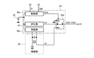
- the stylus 2 includes a core body 20, an electrode 21, a writing pressure detection unit 22, a switch 23, a signal processing unit 24, and a power source 25.
- the core body 20 is a rod-like member arranged so that its longitudinal direction coincides with the pen axis direction of the stylus 2, and constitutes the pen tip of the stylus 2.
- a conductive material is applied to the surface of the distal end portion of the core body 20 to constitute the electrode 21.
- the rear end portion of the core body 20 is in contact with the writing pressure detection unit 22.
- the writing pressure detection unit 22 applies pressure to the tip of the core body 20 (writing pressure applied to the core body 20) when the pen tip of the stylus 2 is pressed against the touch surface 3a (described later) of the position detection device 3 or the like.
- it is constituted by a variable capacitance module whose capacitance changes according to the writing pressure.
- the electrode 21 is a conductor provided in the vicinity of the core body 20 and is electrically connected to the signal processing unit 24 by wiring.
- the signal processing unit 24 supplies the downlink signal DS to the electrode 21, a charge corresponding to the supplied downlink signal DS is induced in the electrode 21.
- a change occurs in the capacitance in the sensor 30 described later, and the position detection device 3 receives the downlink signal DS by detecting this change.
- the uplink signal US transmitted from the position detection device 3 arrives at the electrode 21, a charge corresponding to the incoming uplink signal US is induced at the electrode 21.
- the signal processing unit 24 receives the uplink signal US by detecting the charge induced in the electrode 21 in this way.
- the switch 23 is, for example, a side switch provided on the side surface of the casing of the stylus 2 and functions as an input unit configured to be able to accept an operation by the user.
- the switch information SW shown in FIG. 4 or the like to be described later is output in accordance with the state of operation (pressed state) by the user.
- the switch information SW is information indicating one of two states, for example, on and off.
- the signal processing unit 24 generates a downlink signal DS (downlink signals DS1 and DS2) and a function of receiving the uplink signal US transmitted from the position detection device 3 via the electrode 21, and directs the signal to the position detection device 3. And a function of transmitting via the electrode 21.
- the uplink signal US may include a command as will be described later.
- the signal processing unit 24 acquires a command by demodulating and decoding the received uplink signal US, and generates a downlink signal DS according to the acquired command.
- the power source 25 is for supplying operating power (DC voltage) to the signal processing unit 24, and is composed of, for example, a cylindrical AAAA battery.
- the position detection device 3 includes a sensor 30 that constitutes the touch surface 3 a, a sensor controller 31, and a system controller 32 that controls each part of the position detection device 3 including these.
- the sensor controller 31 has a function of receiving the downlink signal DS transmitted from the stylus 2 via the sensor 30 and a function of transmitting the uplink signal US toward the stylus 2 via the sensor 30.
- the sensor controller 31 is of a type that can receive the downlink signal DS1 but cannot receive the downlink signal DS2 (only in the first method described above).
- the position detection device 3 There is a corresponding position detection device 3) and a type that can receive the downlink signal DS2 but cannot receive the downlink signal DS1 (the position detection device 3 corresponding to only the second method described above).
- the position detection device 3 can be operated with lower power consumption than the alternate transmission method described later with reference to FIGS. 4 to 9. It is characterized in that the stylus 2 does not have to be changed every time it moves.
- FIG. 2 is a diagram illustrating an example of a usage state of the position detection system 1.
- two types of position detecting devices 3A and 3B which are the position detecting devices 3 shown in FIG. 1, are arranged side by side on one desk, and one user uses one stylus 2.
- a picture is input to the position detection device 3A and a sentence is input to the position detection device 3B.
- the present invention is effective in such a case.
- the position detection devices 3A and 3B are each connected to a server (not shown) via the access point 5, and the server receives a picture input to the position detection device 3A and the position detection device 3B.
- the input text is integrated as one document.
- FIG. 3 is a diagram showing a configuration of the position detection device 3.
- the figure collectively shows the configurations of the two types of position detection devices 3 described above, and the part relating to the transmission of the uplink signal US is a configuration specific to the position detection device 3 of the type capable of receiving the downlink signal DS2. It is.
- the position detection device 3 of a type that cannot receive the downlink signal DS2 does not have a function of transmitting the uplink signal US.
- the sensor 30 has a configuration in which a plurality of linear electrodes 30X and a plurality of linear electrodes 30Y are arranged in a matrix, and the stylus 2 and the capacitance are formed by the linear electrodes 30X and 30Y. Join.
- This sensor 30 is used not only for detecting the stylus 2 but also for detecting a finger.
- the sensor controller 31 includes a transmission unit 60, a selection unit 40, a reception unit 50, a logic unit 70, and an MCU 80.
- the transmission unit 60 is a circuit for transmitting the uplink signal US shown in FIG. Specifically, it includes a pattern supply unit 61, a switch 62, a diffusion processing unit 63, a code string holding unit 64, and a transmission guard unit 65.
- the pattern supply unit 61 is described as being included in the transmission unit 60 in the present embodiment, but may be included in the MCU 80.
- the pattern supply unit 61 holds the detection pattern c1, and in accordance with an instruction of the control signal ctrl_t1 supplied from the logic unit 70, a signal corresponding to the detection pattern c1 (or for a predetermined continuous transmission period (for example, 3 msec)) (or Bit string) continuously and repeatedly. Also, it has a function of outputting a predetermined delimiter pattern STP continuously at least twice immediately after the end of the continuous transmission period or at the start of transmission of control information c2 described later.
- the detection pattern c1 is a pattern of symbol values used by the stylus 2 to detect the presence of the sensor controller 31, and is made known to the stylus 2 in advance (before the stylus 2 detects the sensor controller 31).
- a symbol is a unit of information used for modulation in transmission processing (a unit of information expressed by a transmission signal), and is a unit of information obtained by demodulating one symbol that is a reception signal in reception processing.
- the symbol value includes a value converted into a bit string (hereinafter referred to as “bit string corresponding value”) and a value not converted into a bit string by the stylus 2 that has received the symbol (hereinafter referred to as “bit string non-corresponding value”). Can be included.
- the former symbol takes the value of the power of 2 and can be associated with a bit string such as “0001”.
- the bit length of each symbol represented by the bit string is determined by the specification of the diffusion processing unit 63.
- the symbol relating to the latter takes one or more (for example, two) values, and takes a value that is not associated with a bit string such as “P” or “M” as shown in Table 1 described later.
- P and M are associated with a predetermined spreading code string and its inverted code string, respectively.
- the detection pattern c1 is represented by a pattern of non-bit string values. Specifically, it is configured by repeating two bit string non-corresponding values “P” and “M” like “PMPMPM.
- the delimiter pattern STP is a symbol pattern for notifying the stylus 2 of the end of the continuous transmission period, and is configured by a symbol pattern that does not appear during the repetition of the detection pattern c1.
- the detection pattern c1 is configured by repeating two bit string non-corresponding values “P” and “M” like “PMPMPM...”
- the delimiter pattern STP is a bit string non-corresponding value. It can be constituted by a pattern “PP” in which “P” is continued twice.
- the configuration of the separation pattern STP and the detection pattern c1 may be reversed, the separation pattern may be configured by “PM”, and the detection pattern c1 may be configured by “PP”.
- the switch 62 has a function of selecting one of the pattern supply unit 61 and the MCU 80 based on the control signal ctrl_t2 supplied from the logic unit 70 and supplying the selected one output to the diffusion processing unit 63.
- the switch 62 selects the pattern supply unit 61, the detection pattern c1 or the delimiter pattern STP is supplied to the diffusion processing unit 63.
- the switch 62 selects the MCU 80, the diffusion processor 63 is supplied with the control information c2 from the MCU 80.
- the control information c2 is information including a command indicating the instruction content to the stylus 2, and is generated by the MCU 80.
- the control information c2 includes a symbol value (for example, 0 to 15) associated with a variable-length bit string, and is different from the detection pattern c1 in that the value is not shared with the stylus 2 in advance.
- the control information c2 is indicated by a value “D” indicating the number of powers of 2 (eight values) of the predetermined bit length described above, and includes a detection pattern c1 including values “P” and “M”. Is different.
- the code string holding unit 64 has a function of generating and holding an 11-chip long spreading code PN having autocorrelation characteristics based on the control signal ctrl_t3 supplied from the logic unit 70.
- the spreading code PN held by the code string holding unit 64 is supplied to the spreading processing unit 63.
- the spreading processing unit 63 modulates the spreading code PN held by the code string holding unit 64 based on the value of the symbol supplied via the switch 62 (information expressed by the transmission signal by the processing of the spreading processing unit 63). By doing so, it has a function of obtaining a 12-chip long transmission chip array. Hereinafter, this function will be described with a specific example.
- each of the detection pattern c1, the delimiter pattern STP, and the control information c2 includes a bit string corresponding value 0 to 15 (corresponding bit string “0000” to “1111”) and a bit string non-corresponding value “P” “M”. It shall consist of the combination of. Further, it is assumed that the spreading code PN held by the code string holding unit 64 is “00010010111”. In this case, the spread processing unit 63 converts the value of each symbol (0 to 15 and P and M) into a transmission chip sequence according to Table 1 below.
- the symbol value “P” is converted into a transmission chip sequence in which “1” is added to the head of the spread code PN “00010010111”.
- Symbol values “0” to “7” are respectively transmitted to a transmission chip sequence in which “1” is added to the head of a code sequence obtained by cyclically shifting the spread code PN “00010010111” by the shift amount shown in Table 1.
- the other symbol values “M” “8” to “15” are converted into transmission chip sequences obtained by inverting the transmission chip sequences corresponding to the symbol values “P” “0” to “7”, respectively.
- the diffusion processing unit 63 is configured to acquire the transmission chip sequence by the conversion processing as described above and supply it to the transmission guard unit 65.
- the transmission guard unit 65 Based on the control signal ctrl_t4 supplied from the logic unit 70, the transmission guard unit 65 switches between the transmission operation and the reception operation between the transmission period of the uplink signal US and the reception period for receiving the signal from the stylus 2. Therefore, it has a function of inserting a guard period, which is a period during which neither transmission nor reception is performed.
- the selection unit 40 is a switch that switches between a transmission period in which a signal is transmitted from the sensor 30 and a reception period in which the signal is received by the sensor 30 based on the control of the logic unit 70. More specifically, the selection unit 40 includes switches 44x and 44y and conductor selection circuits 41x and 41y. Based on the control signal sTRx supplied from the logic unit 70, the switch 44x connects the output terminal of the transmission unit 60 to the input terminal of the conductor selection circuit 41x during the transmission period, and the conductor selection circuit 41x during the reception period. It operates to connect the output end to the input end of the receiver 50.
- the switch 44y Based on the control signal sTRy supplied from the logic unit 70, the switch 44y connects the output terminal of the transmission unit 60 to the input terminal of the conductor selection circuit 41y during the transmission period, and the conductor selection circuit 41y during the reception period. It operates to connect the output end to the input end of the receiver 50.
- the conductor selection circuit 41x operates to select one or more of the plurality of linear electrodes 30X based on the control signal selX supplied from the logic unit 70 and connect the selected one to the switch 44x.
- the conductor selection circuit 41y operates to select one or more of the plurality of linear electrodes 30Y based on the control signal selY supplied from the logic unit 70 and connect the selected one to the switch 44y.
- the plurality of linear electrodes 30X or the plurality of linear electrodes 30Y are selected by the conductor selection circuits 41x and 41y, for example, when the uplink signal US is transmitted from the entire touch surface 3a.
- the receiving unit 50 is a circuit for receiving the downlink signal DS (downlink signal DS1 or downlink signal DS2) transmitted by the stylus 2 based on the control signal ctrl_r of the logic unit 70.
- the amplifier circuit 51 includes a detection circuit 52, a detection circuit 52, and an analog-digital (AD) converter 53.
- the amplification circuit 51 amplifies and outputs the downlink signal DS supplied from the selection unit 40.
- the detection circuit 52 is a circuit that generates a voltage corresponding to the level of the output signal of the amplifier circuit 51.
- the AD converter 53 is a circuit that generates a digital signal by sampling the voltage output from the detection circuit 52 at predetermined time intervals. The digital signal output from the AD converter 53 is supplied to the MCU 80.
- the receiving unit 50 included in the position detection device 3 of a type that can receive the downlink signal DS1 but cannot receive the downlink signal DS2 receives an unmodulated pulse train signal or a signal obtained by modulating the pulse train signal.
- the modulation sine wave signal or a signal obtained by modulating the sine wave signal is not received (or cannot be received). Therefore, a digital signal is supplied to the MCU 80 in this case from the receiving unit 50 only when the downlink signal DS1 arrives at the sensor 30.
- the receiving unit 50 included in the position detection device 3 of a type that can receive the downlink signal DS2 but cannot receive the downlink signal DS1 receives an unmodulated sine wave signal or a signal obtained by modulating a sine wave signal.
- an unmodulated pulse train signal or a signal obtained by modulating a pulse train signal is not received (or cannot be received). Therefore, a digital signal is supplied from the receiving unit 50 to the MCU 80 in this case only when the downlink signal DS2 arrives at the sensor 30.
- the logic unit 70 and the MCU 80 are control units that control transmission / reception operations of the transmission unit 60, the reception unit 50, and the like.
- the MCU 80 is a microprocessor that has a ROM and a RAM therein and operates based on a predetermined program.
- the logic unit 70 is configured to output each control signal described above based on the control of the MCU 80.
- the MCU 80 also derives coordinate data x, y and the like indicating the position of the stylus 2 based on the digital signal supplied from the AD converter 53, outputs the coordinate data to the system controller 32, and supplies the coordinate data from the AD converter 53.
- the process is configured to perform processing for acquiring the data Res represented by the digital signal and outputting the data Res to the system controller 32.
- the configuration of the stylus 2 and the processing performed by the stylus 2 will be described in detail.
- the stylus 2 that employs the above-described alternate transmission method will be described, and then, according to the first to fifth embodiments of the present invention.
- the stylus 2 will be described.
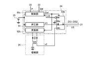
- FIG. 4 is a diagram showing the configuration of the stylus 2 according to the background art of the present invention.
- the stylus 2 shown in the figure adopts the above-described alternate transmission method and corresponds to the background art of the present invention, but the stylus 2 of the present invention is similar to the stylus 2 according to the first to fifth embodiments described later. It was invented by the inventor and was not publicly known as of the priority date of the present application.
- the stylus 2 that employs the alternating transmission method includes an amplification unit 26 in addition to the signal processing unit 24 and the power supply 25 shown in FIG. 1.
- the signal processing unit 24 includes a control unit 90a, a boosting unit 91, an oscillation unit 92a, and a switch unit 93a. 4 does not show a function related to reception of the uplink signal US among the functions of the signal processing unit 24, but an alternate transmission method is used as in the stylus 2 according to each embodiment of the present invention to be described later.
- the employed stylus 2 can also be provided with a function related to reception of the uplink signal US.
- the booster 91 has a function of generating the DC voltage V1 by boosting the DC voltage supplied from the power supply 25.
- the booster 91 is configured by a DC-DC converter or a charge pump circuit.
- the oscillation unit 92a has a function of generating an unmodulated sine wave signal (carrier wave signal) that oscillates at a predetermined frequency by performing an oscillation operation based on a DC voltage supplied from the power supply 25.
- the amplifying unit 26 has a function of generating an unmodulated sine wave signal v2 by amplifying the sine wave signal generated by the oscillating unit 92a with a predetermined amplification factor. As shown in FIG. 4, the amplifying unit 26 is preferably configured by an amplifying circuit including a transformer and a capacitor.
- the switch unit 93a is a single-pole three-throw type switch element, and includes a terminal a connected to the output terminal of the booster unit 91, a terminal b connected to the output terminal of the amplifier unit 26, and a power source to which a ground potential is supplied. A terminal g connected to the wiring and a common terminal c connected to the electrode 21 are configured.
- the control unit 90a is an IC that supplies a control signal Ctrl for controlling the switch unit 93a, and is configured to operate with power supplied from the power supply 25.
- the control unit 90a may be an ASIC or MCU.
- the control unit 90a controls the switch unit 93a so as to function as a first switch unit provided between the output terminal of the booster unit 91 and the electrode 21. That is, a process of switching the switch unit 93a between a state where the terminal a is connected to the common terminal c and a state where the terminal g is connected to the common terminal c is performed.
- the state in which the terminal a is connected to the common terminal c corresponds to the state in which the first switch unit is on, and the state in which the terminal g is connected to the common terminal c is that the first switch unit is off. Corresponds to the state.
- the control unit 90a performs switching control of the switch unit 93a periodically at a predetermined cycle.
- the DC voltage V1 becomes the output voltage of the switch section 93a.
- the ground potential becomes the output voltage of the switch section 93a. Therefore, an unmodulated pulse train signal is output from the switch section 93a, and this becomes the burst signal d1B.
- the control unit 90a performs switching control of the switch unit 93a according to the data Res such as the writing pressure level P and the switch information SW.
- the data Res may include other information such as identification information of the stylus 2.
- the control unit 90a generates a data signal d1D that is a pulse train signal modulated based on the data Res by this switching control.
- FIG. 5 is a diagram illustrating an example of the data signal d1D generated by the control unit 90a (in the case of an on / off modulated pulse train signal).
- the control unit 90a switches the switch unit 93a to the terminal a side when the transmission target bit of the data Res is “1”, and switches the switch unit 93b when the transmission target bit of the data Res is “0”. Switch to terminal g side.
- FIG. 6 is a diagram showing another example of the data signal d1D generated by the control unit 90a (in the case of a frequency-modulated pulse train signal).
- the control unit 90a performs switching control of the switch unit 93b at a frequency corresponding to the value of the data Res.
- the data signal d1D in this case is a pulse train signal that vibrates at a frequency corresponding to the value of the data Res.
- the control unit 90a in the case of transmitting the downlink signal DS2 controls the switch unit 93a so as to function as a second switch unit provided between the output terminal of the amplification unit 26 and the electrode 21. That is, a process of switching the switch unit 93a between a state where the terminal b is connected to the common terminal c and a state where the terminal g is connected to the common terminal c is performed.
- the state in which the terminal b is connected to the common terminal c corresponds to the state in which the second switch unit is on, and the state in which the terminal g is connected to the common terminal c is that the second switch unit is off. Corresponds to the state.
- the control unit 90a fixes the switch unit 93a to the terminal b side. Therefore, an unmodulated sine wave signal v2 is output from the switch section 93a, which becomes a burst signal d2B.
- the control unit 90a performs switching control of the switch unit 93a based on the data Res such as the writing pressure level P and the switch information SW. Even in this case, the data Res may include other information such as identification information of the stylus 2.
- the control unit 90a generates a data signal d2D, which is a sine wave signal modulated based on the data Res, by this switching control.
- On-off modulation is adopted as a specific method of modulating the sine wave signal by the control unit 90a.
- FIG. 7 is a diagram illustrating an example of the data signal d2D generated by the control unit 90a (in the case of a sine wave signal subjected to on / off modulation).
- the control unit 90a switches the switch unit 93a to the terminal b side when the transmission target bit of the data Res is “1”, and switches the switch unit 93b to the terminal g side when the transmission target bit of the data Res is “0”. Switch to.
- the data signal d2D becomes a sine wave signal v2 when the transmission target bit is “1”, and is fixed to the ground potential when the transmission target bit is “0”. Become.
- the control unit 90a first performs the Manchester encoding of the data Res, and performs the switching control of the switch unit 93a based on the Manchester encoded data Res.
- the data signal d2D may be generated.
- control unit 90a is configured to alternately transmit the downlink signal DS1 and the downlink signal DS2. This is so that both the position detection device 3 corresponding only to the downlink signal DS1 and the position detection device 3 corresponding only to the downlink signal DS2 can receive the transmission signal of the stylus 2. Since the downlink signals DS1 and DS2 are alternately transmitted, the inventor of the present application calls the “alternate transmission method”. This will be specifically described below.
- FIG. 8 is a flowchart showing processing performed by the control unit 90a.
- FIG. 9 is a diagram illustrating an example of a signal generated by the control unit 90a.
- the horizontal axis indicates time
- the upper side of the horizontal axis indicates transmission Tx
- the lower side indicates reception Rx.
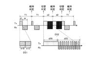
- the control unit 90a is configured to repeat the transmission processing of the downlink signals DS1 and DS2 at a constant period T1.
- the control unit 90a performs each of the burst signal d1B of the downlink signal DS1, the data signal d1D of the downlink signal DS1, the burst signal d2B of the downlink signal DS2, and the data signal d2D of the downlink signal DS2.
- the transmission of the downlink signal DS1 is performed using the time d1 (d1 ⁇ T1) during the period T1
- T1 and d2 indicate that the transmission period of the downlink signal DS2 by the control unit 90a is a stylus corresponding to only the transmission of the downlink signal DS2 (that is, does not have a transmission function of the downlink signal DS1). It is preferable to select to be equal to the transmission cycle of the downlink signal DS2 by the stylus. By doing so, on the sensor controller 31 side, it is possible to receive the downlink signal DS2 in the same cycle as when a stylus corresponding only to the transmission of the downlink signal DS2 transmits.
- the transmission data amount may be reduced for one or both of the burst signal d2B and the data signal d2D.
- the control unit 90a has only M (M ⁇ N) symbols in one cycle of the cycle T1. May be transmitted.
- the section hatched with polka dots in FIG. 9 represents the section in which the sine wave signal v2 is transmitted.
- the data signal d2D is an intermittently transmitted signal. As described with reference to FIG. 7, this corresponds to the fact that the signal processing unit 24 does not output the sine wave signal v ⁇ b> 2 when the transmission target bit is “0”.
- the control unit 90a when starting the processing, the control unit 90a first starts transmitting the downlink signal DS1 (step S1). Thereafter, the passage of time is monitored while transmitting the downlink signal DS1 (step S2), and when the predetermined time d1 has elapsed, transmission of the downlink signal DS2 is started (step S3). Thereafter, the elapse of time is monitored while transmitting the downlink signal DS2 (step S4), and when the predetermined time d2 elapses, the process returns to step S1 and starts transmitting the downlink signal DS1 again. In this way, the control unit 90a alternately transmits the downlink signals DS1 and DS2. As a result, it is possible for both the position detection device 3 corresponding to only the downlink signal DS1 and the position detection device 3 corresponding to only the downlink signal DS2 to receive the transmission signal of the stylus 2.
- both the downlink signals DS1 and DS2 are always transmitted repeatedly.
- one of the downlink signals DS1 and DS2 is always transmitted in vain, which is not preferable from the viewpoint of reducing the power consumption of the stylus 2 as described above.
- the present invention pays attention to such a problem of the alternate transmission method, and achieves lower power consumption than the alternate transmission method and does not have to change the stylus every time the position detecting device 3 is moved.
- first to fifth embodiments of the present invention will be described in detail.
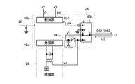
- FIG. 10 is a diagram showing the configuration of the stylus 2 according to the first embodiment of the present invention.
- the stylus 2 shown in the figure is different from the stylus 2 shown in FIG. 4 in that a control unit 90b and a switch unit 93b are provided instead of the control unit 90a and the switch unit 93a. Since the other points are the same as those of the stylus 2 shown in FIG. 4, the same components are denoted by the same reference numerals, and the following description will be made paying attention to different points.
- the switch unit 93b is a single-pole four-throw type by adding a terminal r to the switch unit 93a.
- the terminal r is connected to the receiving terminal of the control unit 90b via a buffer.
- the control unit 90b is configured to operate in one of the first and second modes, in addition to the reception function of the uplink signal US added to the control unit 90a.
- the control unit 90b is configured to perform transmission and reception in a time division manner. That is, the control unit 90b is not configured to perform transmission and reception at the same time.
- the basic operation of the control unit 90b for transmission is as described above for the control unit 90a.
- the control unit 90b switches the switch unit 93b to the terminal r side by the control signal Ctrl.
- the control unit 90b receives the uplink signal US transmitted by the position detection device 3 based on the supplied charge. .
- the first mode is a mode in which the stylus 2 transmits the downlink signal DS1.
- the second mode is a mode in which the stylus 2 transmits the downlink signal DS2.
- the control unit 90b generates the downlink signal DS1 by the above-described process and supplies the downlink signal DS1 to the electrode 21, while performing a process for determining whether or not it is necessary to switch to the second mode.
- the downlink signal DS2 is generated and supplied to the electrode 21 by the above-described processing, and processing for determining whether or not switching to the first mode is necessary is performed.
- the controller 90b makes these determinations based on whether or not the uplink signal US is received in each mode. If it is determined that the switching to the second mode is necessary as a result of the determination, the own operation is switched to the operation in the second mode. Further, when it is determined that switching to the first mode is necessary, its own operation is switched to the operation in the first mode. This will be specifically described below.
- FIG. 11 to 13 are flowcharts showing processing performed by the control unit 90b.
- FIG. 14 is a diagram illustrating an example of a signal generated by the control unit 90b.
- the horizontal axis indicates time
- the upper side of the horizontal axis indicates transmission Tx
- the lower side indicates reception Rx.
- the controller 90b is configured to intermittently transmit the downlink signal DS1 at a constant cycle T1 (predetermined first cycle) also shown in FIG. This is the operation in the first mode. More specifically, the control unit 90b is configured to transmit the downlink signal DS1 over a predetermined time d1 shorter than the period T1 from the beginning of each period T1. Since the downlink signal DS1 is transmitted intermittently in this way, there is always a period during which no transmission operation is performed in the period T1. Using this period, the controller 90b performs an operation of detecting the uplink signal US transmitted from the position detection device 3 using the electrode 21. Then, the necessity of switching to the second mode is determined according to the detection result. Therefore, the control unit 90b determines whether or not it is necessary to switch to the second mode at the cycle T1.
- T1 predetermined first cycle
- the controller 90b after switching to the second mode is configured to intermittently transmit the downlink signal DS2 at a constant period d2 (predetermined second period).
- the time length of the period d2 may or may not be equal to the predetermined time d2 shown in FIG.
- the signal processing unit 24 outputs the sine wave signal v2, while the transmission target bit. Is “0”, this is realized by not outputting the sine wave signal v 2 from the signal processing unit 24. Therefore, intermittent transmission of the downlink signal DS2 is performed during transmission of the data signal d2D instead of the burst signal d2B, as shown in FIG.
- the control unit 90b uses the period in which the sine wave signal v2 is not output from the signal processing unit 24 due to the intermittent transmission, and performs the detection operation of the uplink signal US transmitted by the position detection device 3 using the electrode 21. Do. Then, it is determined whether or not it is necessary to switch to the first mode for each cycle d2 according to the detection result.
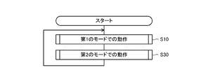
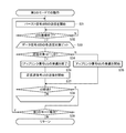
- control unit 90b alternately executes a subroutine (step S10) for performing the operation in the first mode and a subroutine (step S30) for performing the operation in the second mode.
- step S10 for performing the operation in the first mode
- step S30 for performing the operation in the second mode.
- this process does not necessarily switch between step S ⁇ b> 10 and step S ⁇ b> 30 according to the passage of time, but requires mode switching to be executed in each subroutine.
- This is different from the process of the control unit 90a shown in FIG. 8 in that it is performed based on the result of the determination process of NO.
- the processing in each of steps S10 and S30 will be described in detail.
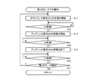
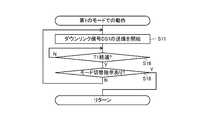
- FIG. 12 is a flowchart showing details of the operation in the first mode (step S10 shown in FIG. 11).
- the control unit 90b operating in the first mode starts transmission of the downlink signal DS1 (including the burst signal d1B and the data signal d1D) (step S11). Thereafter, the passage of time is monitored while transmitting the downlink signal DS1 (step S12), and when the predetermined time d1 has elapsed, reception of the uplink signal US is started (step S13).
- step S14 when the predetermined time dr (dr ⁇ T1-d1) has elapsed (step S14), the reception of the uplink signal US is terminated (step S15), and after the predetermined period T1 has elapsed (step S16), the first It is determined whether or not to maintain this mode (step S17).
- the control unit 90b performs the current subroutine execution (more specifically, from the start of reception of the uplink signal US in step S13 to the end of reception of the uplink signal US in step S15).
- the stylus 2 determines that the first mode is not maintained (that is, switched to the second mode) so that the stylus 2 can transmit the downlink signal DS2. To do. On the contrary, if the uplink signal US is not received during the current subroutine execution, it is determined that the position detection device 3 that can receive the downlink signal DS2 does not exist near the stylus 2, and the first mode Is maintained (that is, it is not switched to the second mode).
- step S17 When it determines with maintaining a 1st mode by step S17, the control part 90b returns to step S11 and continues a process. That is, the subroutine of step S10 shown in FIG. 11 (operation in the first mode shown in FIG. 12) is repeated. On the other hand, when it is determined in step S17 that the first mode is not maintained, the control unit 90b exits the subroutine of step S10 and continues the process. Thereby, the subroutine of step S30 shown in FIG. 11 (operation in the second mode shown in FIG. 13) is started.
- FIG. 13 is a flowchart showing details of the operation in the second mode (step S30 shown in FIG. 11).
- the control unit 90b operating in the second mode first starts transmitting the burst signal d2B (step S31).
- the transmission time of the burst signal d2B is determined in advance, and then the control unit 90b determines whether or not the transmission of the burst signal d2B is completed by determining whether or not the predetermined transmission time has expired. Determination is made (step S32).
- control unit 90b sequentially targets each transmission target bit (each bit of the data Res. Each bit of the Manchester encoded data Res when performing the Manchester encoding) constituting the data signal d2D.
- a loop process is performed (step S33). This loop process is repeated until the period d2 elapses (step S38).
- step S34 the control unit 90b first determines whether or not the transmission target bit is “1” (step S34). In this process, a negative determination is made when the transmission target bit is “0”. Note that the determination result in step S ⁇ b> 34 when there is no transmission target data Res may be negative as in the case where the transmission target bit is “0”.
- step S34 If a negative result is obtained in step S34, the control unit 90b starts receiving the uplink signal US (step S35). On the other hand, when a positive result is obtained in step S34, the control unit 90b ends the reception operation of the uplink signal US when the reception operation of the uplink signal US is performed (step S36). Transmission of the 1-bit sine wave signal v2 is started (step S37).
- step S38 After starting the reception of the uplink signal US in step S35 or starting the transmission of the sine wave signal v2 in step S37, the control unit 90b determines whether or not the period d2 has elapsed (step S38). . If it is determined that it has not elapsed, the process returns to step S34, and the process is repeated for the next transmission target bit. On the other hand, if it is determined in step S38 that the time has elapsed, it is determined whether or not the second mode is maintained by exiting the loop process (step S39).
- the determination criterion in step S39 is the same as the determination criterion in step S17 shown in FIG. That is, the control unit 90b performs the current subroutine (more specifically, from the start of reception of the uplink signal US in step S35 to the end of reception of the uplink signal US in step S36).
- the control unit 90b performs the current subroutine (more specifically, from the start of reception of the uplink signal US in step S35 to the end of reception of the uplink signal US in step S36).
- the second mode when the uplink signal US has been received in the period of time multiple times), it is determined to maintain the second mode (that is, do not switch to the first mode), Conversely, when the uplink signal US is not received during the current subroutine execution, it is preferable to determine that the second mode is not maintained (that is, the mode is switched to the first mode).
- step S39 When it determines with maintaining a 2nd mode by step S39, the control part 90b returns to step S31 and continues a process. Thereby, the subroutine of step S30 shown in FIG. 11 (operation in the second mode shown in FIG. 13) is repeated. On the other hand, when it is determined in step S39 that the second mode is not maintained, the control unit 90b exits the subroutine of step S30 and continues the process. Thereby, the subroutine of step S10 shown in FIG. 11 (operation in the first mode shown in FIG. 12) is started.
- the stylus 2 side determines whether or not mode switching is necessary, and the operation mode of the stylus 2 itself is switched according to the result.
- the operation mode of the stylus 2 is used together with the position detection device 3 corresponding only to the reception of the downlink signal DS1, it is set as the first mode, and used with the position detection device 3 corresponding to reception of the downlink signal DS2 only.
- the second mode can be set. Therefore, when used together with the position detection device 3 (only the first method described above) corresponding to reception of the downlink signal DS1, the downlink signal DS2 is not transmitted and the downlink signal DS2 is not transmitted.
- the stylus can be configured not to use the downlink signal DS1 when used together with the position detection device 3 (only the second method described above) corresponding to reception of the stylus, the stylus can be configured.
- the position detecting devices 3 are used side by side, the power consumption is lower than that of the stylus 2 employing the alternate transmission method shown in FIG. 4, and the stylus does not have to be changed every time the position detecting device 3 is moved. Is possible.
- FIG. 15 is a diagram showing a configuration of the stylus 2 according to the second embodiment of the present invention.
- the stylus 2 shown in the figure is different from the stylus 2 shown in FIG. 10 in that a control unit 90c is provided instead of the control unit 90b. Since the other points are the same as those of the stylus 2 shown in FIG. 10, the same components are denoted by the same reference numerals, and the following description will be made paying attention to different points.
- the control unit 90c is different from the control unit 90b in the processing in the second mode, and is the same as the control unit 90b in other points. Specifically, it is determined whether the stylus 2 is in use during the operation in the second mode, and the uplink signal US is received only when it is determined that the stylus 2 is not in use. If it is determined that the uplink signal US is not received, the uplink signal US is not received. This will be specifically described below.
- FIG. 16 is a flowchart showing details of the operation in the second mode by the control unit 90c.
- FIG. 17 is a diagram illustrating an example of a signal generated by the control unit 90c.
- the horizontal axis indicates time
- the upper side of the horizontal axis indicates transmission Tx
- the lower side indicates reception Rx.
- the control unit 90c executes the processes of steps S31 and S32 in the same manner as the control unit 90b (see FIG. 13). Thereafter, the control unit 90c determines whether or not the stylus 2 is in use (step S40). This determination may be made based on whether the writing pressure level P is greater than 0, for example. That is, when the writing pressure level P is larger than 0, it is determined that the stylus 2 is in use because the probability that the stylus 2 is touching the touch surface 3a is high, and when the writing pressure level P is 0 or less, the stylus is used. What is necessary is just to determine that 2 is not in use since the probability that 2 is away from the touch surface 3a is high. Further, when the switch information SW is on, it may be determined that the stylus 2 is in use. In this case, it is possible to determine whether or not the stylus 2 is in use by the user's intention.
- the controller 90c determines that it is in use at step S40, it starts transmission of the data signal d2D (step S41).
- This transmission is intermittent as shown in FIG. 17 because the sine wave signal v2 is not output from the signal processing unit 24 when the transmission target bit is “0” as described above.
- the control unit 90b performs the reception operation of the uplink signal US using the interval between the intermittent transmissions, the control unit 90c does not perform such reception operation as shown in FIG.
- the reason why such a process is adopted is that the stylus 2 is in the vicinity of the position detecting device 3 that can continuously receive the downlink signal DS2 since it is determined in step S40 that it is in use. This is because there is no need to switch to the first mode.
- Step S40 the control unit 90c when determining that it is not in use in Step S40 starts receiving the uplink signal US (Step S42).
- the receiving operation in this case is continuously performed as shown in FIG.
- Such a continuous reception operation is possible because it is considered unnecessary to send the data signal d2D when not in use, and therefore the data signal d2D is not transmitted.
- control unit 90c continues transmission of the data signal d2D or reception of the uplink signal US until the period d2 elapses (step S43), and determines that the period d2 elapses in step S43. It is determined whether or not to maintain this mode (step S44).
- step S44 if the reception operation in step S42 is not performed (that is, if it is determined in step S40 that the stylus 2 is in use), the second mode is unconditionally maintained. Judgment is made. Therefore, in this case, step S44 can be omitted.
- step S42 it is determined whether or not to maintain the second mode based on the same determination criteria as in step S39 shown in FIG.
- step S44 When it determines with maintaining a 2nd mode by step S44, the control part 90c returns to step S31 and continues a process. Thereby, the subroutine of step S30 shown in FIG. 11 (operation in the second mode shown in FIG. 16) is repeated. On the other hand, when it is determined in step S44 that the second mode is not maintained, the control unit 90c exits the subroutine of step S30 and continues the process. Thereby, the subroutine of step S10 shown in FIG. 11 (operation in the first mode shown in FIG. 12) is started.
- the stylus 2 according to the present embodiment in addition to the same effects as the stylus 2 according to the first embodiment, it can be improved over a longer period than the first embodiment.
- the effect that the link signal US can be continuously received is obtained. Thereby, it is possible to receive the uplink signal US with higher accuracy than in the first embodiment.
- FIG. 18 is a diagram showing a configuration of the stylus 2 according to the third embodiment of the present invention.
- the stylus 2 shown in the figure is different from the stylus 2 shown in FIG. 10 in that a control unit 90d is provided instead of the control unit 90b. Since the other points are the same as those of the stylus 2 shown in FIG. 10, the same components are denoted by the same reference numerals, and the following description will be made paying attention to different points.
- the control unit 90d determines whether or not it is necessary to switch to the first mode or the second mode based on the user operation received by the switch 23 illustrated in FIG. 1 instead of whether or not the uplink signal US is received. Unlike the control unit 90b, the other points are the same as the control unit 90b. This will be specifically described below.
- FIG. 19 and 20 are flowcharts showing processing performed by the control unit 90d.
- FIG. 21 is a diagram illustrating an example of a signal generated by the control unit 90d.
- the horizontal axis indicates time
- the upper side of the horizontal axis indicates transmission Tx
- the lower side indicates reception Rx.
- FIG. 19 is a flowchart showing details of the operation in the first mode (step S10 shown in FIG. 11).
- the control unit 90d operating in the first mode first executes the process of step S11 in the same manner as the control unit 90b (see FIG. 12). Thereafter, the processing in steps S12 to S15 shown in FIG. 12 is not performed, and the process waits until a predetermined period T1 elapses (step S16). Since the processes in steps S12 to S15 are not performed, the uplink signal US is not received during the operation in the first mode as shown in FIG.
- the control unit 90d determines whether or not there has been a mode switching instruction from the user based on the switch information SW (step S18). In other words, it is determined whether or not it is necessary to switch to the second mode.
- step S18 If it is determined in step S18 that there is no mode switching instruction, the control unit 90d returns to step S11 and continues the process. Thereby, the subroutine of step S10 shown in FIG. 11 (operation in the first mode shown in FIG. 19) is repeated. On the other hand, if it is determined in step S18 that a mode switching instruction has been issued, the control unit 90b exits the subroutine of step S10 and continues the process. Thereby, the subroutine of step S30 shown in FIG. 11 (operation in the second mode shown in FIG. 20) is started.
- FIG. 20 is a flowchart showing details of the operation in the second mode (step S30 shown in FIG. 11).
- the control unit 90d operating in the second mode first executes the processing of steps S31 to S38 in the same manner as the control unit 90b (see FIG. 13). Therefore, transmission / reception of each signal in the second mode is performed in the same manner as in the first embodiment, as shown in FIG. Thereafter, the control unit 90d performs a process (step S50) for determining whether or not there is a mode switching instruction by the user based on the switch information SW, instead of the determination process of step S39 illustrated in FIG. In other words, it is determined whether or not it is necessary to switch to the first mode.
- step S50 If it is determined in step S50 that there has been no mode switching instruction, the control unit 90d returns to step S31 and continues the process. Thereby, the subroutine of step S30 shown in FIG. 11 (operation in the second mode shown in FIG. 20) is repeated. On the other hand, if it is determined in step S50 that there has been a mode switching instruction, the control unit 90d exits the subroutine of step S10 and continues processing. Thereby, the subroutine of step S10 shown in FIG. 11 (operation in the first mode shown in FIG. 19) is started.
- the first mode and the second mode can be switched by an explicit instruction from the user. Therefore, as in the first and second embodiments, in the case where the position detection device 3 corresponding only to reception of the downlink signal DS1 and the position detection device 3 corresponding to reception of the downlink signal DS2 are used side by side.
- the power consumption is lower than that of the stylus 2 that employs the alternate transmission method shown in FIG. 4, and the stylus need not be changed each time the position detection device 3 is moved.
- the process of the control unit 90d is configured by modifying step S39 in the process of the control unit 90b shown in FIG. 13, but the step of the process of the control unit 90c shown in FIG. It is also possible to configure the processing of the control unit 90d by modifying S44 in the same manner. In this case, as in the second embodiment, it is possible to obtain an effect that the uplink signal US can be received with higher accuracy than in the first embodiment.
- FIG. 22 is a diagram showing a configuration of the stylus 2 according to the fourth embodiment of the present invention.
- the stylus 2 shown in the figure is different from the stylus 2 shown in FIG. 10 in that it includes a control unit 90e and an oscillation unit 92b instead of the control unit 90d and the oscillation unit 92a. Since the other points are the same as those of the stylus 2 shown in FIG. 10, the same components are denoted by the same reference numerals, and the following description will be made paying attention to different points.
- the control unit 90e When the control unit 90e generates the data signal d2D constituting the downlink signal DS2, the control unit 90e fixes the switch unit 93b in a state in which the switch unit 93b is switched to the terminal b.
- the oscillation state of the oscillation unit 92b is controlled instead of the switching control of the switch unit 93a. Specifically, when the transmission target bit is “1”, the oscillation unit 92b is in an oscillation state, and when the transmission target bit is “0”, the oscillation unit 92b is in an oscillation stop state.
- the control unit 90e when generating the burst signal d2B fixes the switch unit 93b while switching to the terminal b, and fixes the oscillation unit 92b to the oscillation state.
- the downlink signal DS2 can be transmitted from the stylus 2 in the same manner as the stylus 2 according to the first embodiment.
- the stylus 2 according to the present embodiment is the same as the stylus 2 according to the first embodiment. Therefore, the configuration and operation of the stylus 2 according to the present embodiment are the same as those of the first embodiment.
- the downlink signal DS2 similar to that of the present embodiment may be generated not only by the stylus 2 according to the first embodiment but also by the stylus 2 according to the second and third embodiments. Of course.
- FIG. 23 is a diagram showing a configuration of the stylus 2 according to the fifth embodiment of the present invention.
- the stylus 2 shown in the figure is different from the stylus 2 shown in FIG. 10 in that a rectifier 94 is provided instead of the booster 91. Since the other points are the same as those of the stylus 2 shown in FIG. 10, the same components are denoted by the same reference numerals, and the following description will be made paying attention to different points.
- the rectifying unit 94 is a circuit that generates a DC voltage V1 by rectifying the sine wave signal v2 output from the amplifying unit 26 using a diode and a capacitor.
- the DC voltage V1 generated by the rectifying unit 94 is supplied to the terminal a of the switch unit 93b.
- the downlink signal DS1 can be transmitted from the stylus 2 in the same manner as the stylus 2 according to the first embodiment.
- the stylus 2 according to the present embodiment is the same as the stylus 2 according to the first embodiment. Therefore, the configuration and operation of the stylus 2 according to the present embodiment are the same as those of the first embodiment.
- the boosting unit 91 is not necessary, and thus the configuration of the signal processing unit 24 can be simplified.
- the generation of the DC voltage V1 similar to that in the present embodiment may be performed not only in the stylus 2 according to the first embodiment but also in the stylus 2 according to the second to fourth embodiments.
- the oscillation unit 92b needs to be in an oscillation state when the downlink signal DS1 is transmitted.
- the stylus 2 determines the mode switching based on whether or not the uplink signal US is received, the contents of the uplink signal US are not considered, but the stylus 2 The presence / absence of mode switching may be determined based on the content of the uplink signal US. In this case, the mode of the stylus 2 can be switched by an explicit instruction from the sensor controller 31.
- the uplink signal US is a signal composed of the detection pattern c1, the delimiter pattern STP, and the control information c2.
- the uplink signal US is a simple trigger signal. The present invention can be suitably applied to cases.
Abstract
[Problem]
To enable less power to be consumed than in an alternate transmission method and to eliminate the need to exchange a stylus being used every time the position detection device is changed, when a position detection device compatible only with a first method and a position detection device compatible only with a second method are used side by side.
[Solution]
This active stylus is equipped with a signal processing unit 24 which, when operating in a first mode, supplies to an electrode 21 a downlink signal DS1 produced by modulating a pulse train signal by means of a writing pressure level P, and determines whether it is necessary to switch to a second mode, and when operating in a second mode, supplies to the electrode 21 a downlink signal DS2 produced by modulating a sine-wave signal by means of the writing pressure level P, and determines whether it is necessary to switch to the first mode. The signal processing unit switches to operating in the second mode when it is determined that it is necessary to switch to the second mode, and switches to operating in the first mode when it is determined that it is necessary to switch to the first mode.
Description
本発明はアクティブスタイラスに関し、特に、複数の方式に対応するアクティブスタイラスに関する。
The present invention relates to an active stylus, and more particularly to an active stylus that supports a plurality of systems.
指検出を行うためにタッチパネル内に用意された電極を利用してスタイラスの存在や位置を検出可能としたアクティブ静電方式の位置検出システムが知られている。この種の位置検出システムで用いられるスタイラスは「アクティブスタイラス」と呼ばれ、上記電極との静電結合により、位置検出装置内のセンサコントローラに対して信号を送信するよう構成される。センサコントローラは、この信号を検出することにより、スタイラスの存在や位置を検出する。
There is known an active electrostatic type position detection system capable of detecting the presence and position of a stylus using electrodes prepared in a touch panel for finger detection. A stylus used in this type of position detection system is called an “active stylus” and is configured to transmit a signal to a sensor controller in the position detection device by electrostatic coupling with the electrode. The sensor controller detects the presence and position of the stylus by detecting this signal.
特許文献1には、このようなアクティブスタイラスの一例として、専ら座標データの導出のために使用される位置信号と、筆圧値やスタイラスの固有IDなどの情報を表すデータ信号とをセンサコントローラに対して送信するように構成されたスタイラスが開示されている。
In Patent Document 1, as an example of such an active stylus, a position signal used exclusively for deriving coordinate data and a data signal representing information such as a pen pressure value and a unique ID of the stylus are provided to a sensor controller. A stylus configured to transmit to is disclosed.
特許文献2には、アクティブスタイラスの他の例が開示されている。この例によるスタイラスは、筆圧検出した結果をデジタルで送信している。また、特許文献2では、表示装置及び透明センサによって位置検出装置が構成されており、位置検出装置は、透明センサにより、スタイラスによる指示位置および筆圧と、指によるタッチ位置との両方を検出する。
Patent Document 2 discloses another example of an active stylus. The stylus according to this example digitally transmits the result of detecting the pen pressure. Further, in Patent Document 2, a position detection device is configured by a display device and a transparent sensor, and the position detection device detects both an indication position and writing pressure by a stylus and a touch position by a finger by the transparent sensor. .
ところで近年、静電結合を利用して信号を送信するスタイラスを備えた電子機器が多数登場してきている。そして、これら電子機器に含まれる位置検出システムとして、互いに互換性を有しない複数の信号送信方式が利用されるようになってきている。具体的には、スタイラスが送信する信号として、パルス列信号(パルス信号、矩形波信号を含む)を変調してなる信号を用いる方式(以下、「第1の方式」という)と、正弦波信号を変調してなる信号を用いる方式(以下、「第2の方式」という)とが混在している。
By the way, in recent years, many electronic devices equipped with a stylus that transmits signals using electrostatic coupling have appeared. As a position detection system included in these electronic devices, a plurality of signal transmission methods that are not compatible with each other have been used. Specifically, as a signal transmitted by the stylus, a method using a signal obtained by modulating a pulse train signal (including a pulse signal and a rectangular wave signal) (hereinafter referred to as “first method”) and a sine wave signal are used. A method using a modulated signal (hereinafter referred to as “second method”) is mixed.
特許文献3には、第1の方式に準拠する位置検出システムの一例が開示されている。この例によるスタイラスは、光学的に筆圧を検出する筆圧検出部と信号送信部とを備える。信号送信部が送信する信号には、特許文献3の図10に示されるように、位置検出装置によるスタイラスの位置の検出に用いられる位置信号パルス910と、筆圧検出部によって検出された筆圧のレベルを示す圧力信号パルス950とが含まれる。位置信号パルス910は間欠的に送信され、圧力信号パルス950は、筆圧が検出されているとき(ホバー動作状態でないとき)に限り、位置信号パルス910の送信の合間に送信される。位置信号パルス910は所定周波数(具体的には28.125Hz)のACパルスによって構成され、圧力信号パルス950は周波数変調されたパルス信号によって構成される。
Patent Document 3 discloses an example of a position detection system that conforms to the first method. The stylus according to this example includes a writing pressure detection unit that optically detects writing pressure and a signal transmission unit. As shown in FIG. 10 of Patent Document 3, the signal transmitted by the signal transmission unit includes a position signal pulse 910 used for detecting the position of the stylus by the position detection device, and the writing pressure detected by the writing pressure detection unit. And a pressure signal pulse 950 indicating the level of. The position signal pulse 910 is transmitted intermittently, and the pressure signal pulse 950 is transmitted between transmissions of the position signal pulse 910 only when the pen pressure is detected (not in the hover operation state). The position signal pulse 910 is constituted by an AC pulse having a predetermined frequency (specifically, 28.125 Hz), and the pressure signal pulse 950 is constituted by a frequency-modulated pulse signal.
特許文献4にも、第1の方式に準拠する位置検出システムの一例が開示されている。この例によるスタイラスは、特許文献4の図9に示されるようにTXドライブ回路680を備えており、これにより、指検出時に用いられるTX信号632と同様のパルス列信号であるTX信号677を送信するよう構成される。TX信号677は、スタイラスとセンサとの間の結合容量を介して、コントローラで検出される。
Patent Document 4 also discloses an example of a position detection system that conforms to the first method. The stylus according to this example includes a TX drive circuit 680 as shown in FIG. 9 of Patent Document 4, thereby transmitting a TX signal 677 that is a pulse train signal similar to the TX signal 632 used at the time of finger detection. It is configured as follows. The TX signal 677 is detected by the controller via the coupling capacitance between the stylus and the sensor.
なお、特許文献4には、スタイラスが信号を送信する際の昇圧の仕組みも開示されている([0084]段落)。これによれば、TX信号835の送信を担うチップドライブ回路890によるTX信号835の増幅を可能とするために、ブースター870がスタイラスに設けられる。
Note that Patent Document 4 also discloses a boosting mechanism when the stylus transmits a signal (paragraph [0084]). According to this, a booster 870 is provided on the stylus in order to allow the chip drive circuit 890 responsible for transmitting the TX signal 835 to amplify the TX signal 835.
これに対し、特許文献1,2に開示される位置検出システムは、第2の方式に準拠している。第2の方式によるスタイラスは、指検出時に用いられる信号(センサコントローラから、センサ内の送信電極に送信される信号)のようなパルス列信号ではなく、正弦波信号を筆圧レベル等に応じて変調して送信するよう構成される。具体的には、例えば数百~数MHzの搬送波信号をASKあるいはOOKにより変調し、送信するよう構成される。センサコントローラは、上記周波数の信号を抽出するためにバンドパスフィルタを介して信号を受信し、筆圧値を復元する。
In contrast, the position detection systems disclosed in Patent Documents 1 and 2 comply with the second method. The stylus according to the second method modulates a sine wave signal according to the writing pressure level, not a pulse train signal such as a signal used when detecting a finger (a signal transmitted from the sensor controller to the transmitting electrode in the sensor). Configured to transmit. Specifically, for example, a carrier signal of several hundred to several MHz is modulated by ASK or OOK and transmitted. The sensor controller receives the signal through the bandpass filter to extract the signal having the above frequency, and restores the writing pressure value.
第2の方式のみに対応する位置検出装置は第1の方式のみに対応するスタイラスの送信信号を受信できず、第1の方式のみに対応する位置検出装置は第2の方式のみに対応するスタイラスの送信信号を受信できない。その結果、例えばユーザが第1の方式のみに対応する位置検出装置と第2の方式のみに対応する位置検出装置とを並べて交互に使用しようとする場合、位置検出装置を移るたびにスタイラスを持ち替えねばならなくなっており、不便であった。
A position detection device corresponding only to the second method cannot receive a transmission signal of a stylus corresponding to only the first method, and a position detection device corresponding to only the first method is a stylus corresponding to only the second method. The transmission signal cannot be received. As a result, for example, when the user tries to use a position detection device corresponding to only the first method and a position detection device corresponding to the second method side by side, the stylus is changed every time the position detection device is moved. It was inconvenient because it was necessary.
これに対し、スタイラスを、第1の方式で生成された送信信号(例えばパルス列信号を変調してなる信号)と第2の方式で生成された送信信号(例えば正弦波信号を変調してなる信号)を交互に送信するように構成することが考えられる。以下、スタイラスをこのように構成する方式を「交互送信方式」と称する。交互送信方式によれば、第1の方式のみに対応する位置検出装置と第2の方式のみに対応する位置検出装置とのいずれにもスタイラスの送信信号を受信させることができるので、位置検出装置を移るたびにスタイラスを持ち替える必要はなくなる。しかしながら、一度に両方の位置検出装置を使用することは通常あり得ないので、この方法では、いずれか一方の信号は常に無駄に送信されていることになる。これは、スタイラスの低消費電力化の観点から好ましい状態ではない。
On the other hand, the transmission signal generated by the first method (for example, a signal obtained by modulating a pulse train signal) and the transmission signal generated by the second method (for example, a signal obtained by modulating a sine wave signal) ) May be alternately transmitted. Hereinafter, the method of configuring the stylus in this way is referred to as “alternate transmission method”. According to the alternate transmission method, the position detection device can receive the stylus transmission signal in both the position detection device corresponding to only the first method and the position detection device corresponding to only the second method. You don't have to change your stylus every time you move. However, since it is usually not possible to use both position detecting devices at once, in this method, one of the signals is always transmitted in vain. This is not a preferable state from the viewpoint of reducing the power consumption of the stylus.
したがって、本発明の目的の一つは、第1の方式のみに対応する位置検出装置と第2の方式のみに対応する位置検出装置とを並べて使用する場合において、交互送信方式よりも低消費電力で、位置検出装置を移るたびにスタイラスを持ち替えなくて済むようにすることのできるアクティブスタイラスを提供することにある。
Therefore, one of the objects of the present invention is that when a position detecting device corresponding to only the first method and a position detecting device corresponding to only the second method are used side by side, the power consumption is lower than that of the alternating transmission method. An object of the present invention is to provide an active stylus that can avoid having to change the stylus every time the position detecting device is moved.
本発明によるアクティブスタイラスは、センサとの間で形成される結合容量を介し情報を電界の変化に対応付けてセンサコントローラに対して送信するアクティブスタイラスであって、ペン先を構成する芯体と、前記芯体の近傍に設けられた電極と、前記芯体に加えられた筆圧に応じた筆圧レベルを検出する筆圧検出部と、電源と、前記電源から供給される電力により第1及び第2のモードのいずれか一方で動作し、前記第1のモードでの動作中に、前記筆圧レベルによりパルス列信号が変調されてなる第1の送信信号を前記電極に供給する一方、前記第2のモードへの切り替えの要否を判定し、前記第2のモードでの動作中に、前記筆圧レベルにより正弦波信号が変調されてなる第2の送信信号を前記電極に供給する一方、前記第1のモードへの切り替えの要否を判定し、前記第2のモードへの切り替えが必要であると判定した場合に前記第2のモードでの動作に切り替え、前記第1のモードへの切り替えが必要であると判定した場合に前記第1のモードでの動作に切り替える信号処理部とを備えるアクティブスタイラスである。
An active stylus according to the present invention is an active stylus that transmits information to a sensor controller in association with a change in an electric field via a coupling capacitance formed between the sensor and a core that forms a pen tip; An electrode provided in the vicinity of the core body, a writing pressure detection unit that detects a writing pressure level corresponding to the writing pressure applied to the core body, a power source, and a first power and a power supplied from the power source. While operating in any one of the second modes, the first transmission signal obtained by modulating the pulse train signal by the writing pressure level is supplied to the electrode during the operation in the first mode, Determining whether it is necessary to switch to the second mode, and supplying a second transmission signal obtained by modulating a sine wave signal by the writing pressure level to the electrode during the operation in the second mode, The first module When it is determined whether or not it is necessary to switch to the second mode, and it is determined that switching to the second mode is necessary, the operation is switched to the operation in the second mode, and the switching to the first mode is necessary. An active stylus comprising a signal processing unit that switches to the operation in the first mode when it is determined that there is.
本発明の他の一側面によるアクティブスタイラスは、センサとの間で形成される結合容量を介し情報を電界の変化に対応付けてセンサコントローラに対して送信するアクティブスタイラスであって、ペン先を構成する芯体と、前記芯体の近傍に設けられた電極と、前記芯体に加えられた筆圧に応じた筆圧レベルを検出するための筆圧検出部と、電源と、前記電源から供給される電力により第1及び第2のモードのいずれか一方で動作し、前記第1のモードでの動作中に、前記筆圧レベルによりパルス列が変調された第1の送信信号を前記電極に供給する一方、前記第1の送信信号を送信していない期間に受信した信号により前記第2のモードへの切り替えの要否を判定し、前記第2のモードでの動作中に、前記筆圧レベルにより前記パルス列を変調する変調方式と異なる変調方式により生成された第2の送信信号を前記電極に供給する一方、前記第1のモードへの切り替えの要否を判定し、前記第2のモードへの切り替えが必要であると判定した場合に前記第2のモードでの動作に切り替え、前記第1のモードへの切り替えが必要であると判定した場合に前記第1のモードでの動作に切り替える信号処理部とを備えるアクティブスタイラスである。
An active stylus according to another aspect of the present invention is an active stylus that transmits information to a sensor controller in association with a change in an electric field via a coupling capacitance formed between the sensor and a pen tip. A core body, an electrode provided in the vicinity of the core body, a writing pressure detection unit for detecting a writing pressure level corresponding to the writing pressure applied to the core body, a power source, and a power source supplied from the power source One of the first mode and the second mode is operated by the applied power, and the first transmission signal in which the pulse train is modulated by the writing pressure level is supplied to the electrode during the operation in the first mode. On the other hand, it is determined whether or not it is necessary to switch to the second mode based on a signal received during a period in which the first transmission signal is not transmitted, and the pen pressure level is determined during the operation in the second mode. By the pulse train While supplying to the electrode a second transmission signal generated by a modulation method different from the modulation method to be modulated, it is necessary to determine whether or not to switch to the first mode and to switch to the second mode. A signal processing unit that switches to the operation in the second mode when it is determined to be, and switches to the operation in the first mode when it is determined that the switching to the first mode is necessary. An active stylus is provided.
An active stylus according to another aspect of the present invention is an active stylus that transmits information to a sensor controller in association with a change in an electric field via a coupling capacitance formed between the sensor and a pen tip. A core body, an electrode provided in the vicinity of the core body, a writing pressure detection unit for detecting a writing pressure level corresponding to the writing pressure applied to the core body, a power source, and a power source supplied from the power source One of the first mode and the second mode is operated by the applied power, and the first transmission signal in which the pulse train is modulated by the writing pressure level is supplied to the electrode during the operation in the first mode. On the other hand, it is determined whether or not it is necessary to switch to the second mode based on a signal received during a period in which the first transmission signal is not transmitted, and the pen pressure level is determined during the operation in the second mode. By the pulse train While supplying to the electrode a second transmission signal generated by a modulation method different from the modulation method to be modulated, it is necessary to determine whether or not to switch to the first mode and to switch to the second mode. A signal processing unit that switches to the operation in the second mode when it is determined to be, and switches to the operation in the first mode when it is determined that the switching to the first mode is necessary. An active stylus is provided.
本発明によれば、スタイラス側でモード切り替えの要否を判定し、その結果に応じてスタイラス自身の動作モードを切り替えているので、スタイラスの動作モードを、第1の方式のみに対応する位置検出装置とともに使用する場合には第1のモードとし、第2の方式のみに対応する位置検出装置とともに使用する場合には第2のモードとすることができる。したがって、第1の方式のみに対応する位置検出装置とともに使用する場合には第2の送信信号を送信せず、第2の方式のみに対応する位置検出装置とともに使用する場合には第1の送信信号を送信しないようスタイラスを構成することが可能になるので、第1の方式のみに対応する位置検出装置と第2の方式のみに対応する位置検出装置とを並べて使用する場合において、上述した交互送信方式よりも低消費電力で、位置検出装置を移るたびにスタイラスを持ち替えなくて済むようにすることが可能になる。
According to the present invention, the necessity of mode switching is determined on the stylus side, and the operation mode of the stylus itself is switched according to the result, so that the position detection corresponding to only the first method is performed for the stylus operation mode. The first mode can be used when used with the apparatus, and the second mode can be used when used with the position detecting apparatus corresponding to only the second system. Therefore, the second transmission signal is not transmitted when used with a position detection apparatus corresponding to only the first scheme, and the first transmission is transmitted when used with a position detection apparatus corresponding to only the second scheme. Since the stylus can be configured not to transmit a signal, when the position detection device corresponding to only the first method and the position detection device corresponding to only the second method are used side by side, the above-described alternate With lower power consumption than the transmission method, it becomes possible to avoid having to change the stylus every time the position detecting device is moved.
以下、添付図面を参照しながら、本発明の実施の形態について詳細に説明する。
Hereinafter, embodiments of the present invention will be described in detail with reference to the accompanying drawings.
図1は、本発明の実施の形態による位置検出システム1の構成を示す図である。同図に示すように、位置検出システム1は、スタイラス2と、位置検出装置3とを備えて構成される。
FIG. 1 is a diagram showing a configuration of a position detection system 1 according to an embodiment of the present invention. As shown in FIG. 1, the position detection system 1 includes a stylus 2 and a position detection device 3.
スタイラス2は、位置検出装置3に対してダウンリンク信号DSを送信する機能と、位置検出装置3が送信するアップリンク信号USを受信する機能とを備える位置指示器である。スタイラス2が送信するダウンリンク信号DSには、形式の異なる2種類のダウンリンク信号DS1,DS2(第1及び第2の送信信号)が含まれる。後述する図9に示すように、ダウンリンク信号DS1は、無変調のパルス列信号であるバースト信号d1Bと、パルス列信号を変調してなるデータ信号d1Dとを含む信号である。ダウンリンク信号DS1の具体的な例としては、特許文献3記載の変調方式や、相互容量方式のタッチパネルの送信電極に供給されるパルス列信号と同じように、あるいは、相関をもってスタイラスからパルス列信号を送信する方式によるダウンリンク信号が挙げられる。また、ダウンリンク信号DS2は、無変調の正弦波信号であるバースト信号d2Bと、正弦波信号を変調してなるデータ信号d2Dとを含む信号である。ダウンリンク信号DS2の具体的な例としては、例えばアクティブES(商標)方式で用いられるダウンリンク信号が挙げられる。
The stylus 2 is a position indicator having a function of transmitting a downlink signal DS to the position detection device 3 and a function of receiving an uplink signal US transmitted by the position detection device 3. The downlink signal DS transmitted by the stylus 2 includes two types of downlink signals DS1 and DS2 (first and second transmission signals) having different formats. As shown in FIG. 9 described later, the downlink signal DS1 is a signal including a burst signal d1B that is an unmodulated pulse train signal and a data signal d1D obtained by modulating the pulse train signal. As a specific example of the downlink signal DS1, a pulse train signal is transmitted from the stylus in the same manner as the pulse train signal supplied to the transmission electrode of the modulation method described in Patent Document 3 or the mutual capacitive touch panel, or with a correlation. The downlink signal by the method to do is mentioned. The downlink signal DS2 includes a burst signal d2B that is an unmodulated sine wave signal and a data signal d2D obtained by modulating the sine wave signal. As a specific example of the downlink signal DS2, for example, a downlink signal used in an active ES (trademark) system can be cited.
スタイラス2は、図1に示すように、芯体20、電極21、筆圧検出部22、スイッチ23、信号処理部24、及び電源25を有して構成される。
As shown in FIG. 1, the stylus 2 includes a core body 20, an electrode 21, a writing pressure detection unit 22, a switch 23, a signal processing unit 24, and a power source 25.
芯体20は、その長手方向がスタイラス2のペン軸方向と一致するように配置される棒状の部材であり、スタイラス2のペン先を構成する。芯体20の先端部の表面には導電性材料が塗布され、電極21を構成している。芯体20の後端部は、筆圧検出部22に当接される。筆圧検出部22は、位置検出装置3のタッチ面3a(後述)等にスタイラス2のペン先を押し当てたときに芯体20の先端に加わる圧力(芯体20に加えられた筆圧)に応じた筆圧レベル(後述する図4等に示す筆圧レベルP)を検出するもので、具体的な例では、筆圧に応じて静電容量の変化する可変容量モジュールにより構成される。
The core body 20 is a rod-like member arranged so that its longitudinal direction coincides with the pen axis direction of the stylus 2, and constitutes the pen tip of the stylus 2. A conductive material is applied to the surface of the distal end portion of the core body 20 to constitute the electrode 21. The rear end portion of the core body 20 is in contact with the writing pressure detection unit 22. The writing pressure detection unit 22 applies pressure to the tip of the core body 20 (writing pressure applied to the core body 20) when the pen tip of the stylus 2 is pressed against the touch surface 3a (described later) of the position detection device 3 or the like. In a specific example, it is constituted by a variable capacitance module whose capacitance changes according to the writing pressure.
電極21は、芯体20の近傍に設けられる導電体であり、配線により信号処理部24と電気的に接続されている。信号処理部24がダウンリンク信号DSを電極21に供給すると、電極21には、供給されたダウンリンク信号DSに応じた電荷が誘導される。これにより、後述するセンサ30内の静電容量に変化が生じ、位置検出装置3は、この変化を検出することによりダウンリンク信号DSを受信する。また、位置検出装置3が送信しているアップリンク信号USが電極21に到来すると、電極21には、到来したアップリンク信号USに応じた電荷が誘導される。信号処理部24は、こうして電極21に誘導された電荷を検出することにより、アップリンク信号USを受信する。
The electrode 21 is a conductor provided in the vicinity of the core body 20 and is electrically connected to the signal processing unit 24 by wiring. When the signal processing unit 24 supplies the downlink signal DS to the electrode 21, a charge corresponding to the supplied downlink signal DS is induced in the electrode 21. As a result, a change occurs in the capacitance in the sensor 30 described later, and the position detection device 3 receives the downlink signal DS by detecting this change. Further, when the uplink signal US transmitted from the position detection device 3 arrives at the electrode 21, a charge corresponding to the incoming uplink signal US is induced at the electrode 21. The signal processing unit 24 receives the uplink signal US by detecting the charge induced in the electrode 21 in this way.
スイッチ23は、例えばスタイラス2の筐体の側面に設けられたサイドスイッチであり、ユーザによる操作を受け付け可能に構成された入力部として機能する。具体的には、ユーザによる操作の状態(押下状態)に応じて、後述する図4等に示すスイッチ情報SWを出力するよう構成される。スイッチ情報SWは、例えばオンとオフの2つの状態のいずれか一方を示す情報である。
The switch 23 is, for example, a side switch provided on the side surface of the casing of the stylus 2 and functions as an input unit configured to be able to accept an operation by the user. Specifically, the switch information SW shown in FIG. 4 or the like to be described later is output in accordance with the state of operation (pressed state) by the user. The switch information SW is information indicating one of two states, for example, on and off.
信号処理部24は、位置検出装置3が送信するアップリンク信号USを電極21を介して受信する機能と、ダウンリンク信号DS(ダウンリンク信号DS1,DS2)を生成し、位置検出装置3に向け、電極21を介して送信する機能とを有する。なお、アップリンク信号USは、後述するようにコマンドを含む場合がある。その場合における信号処理部24は、受信したアップリンク信号USを復調及び復号することによってコマンドを取得し、取得したコマンドに従ってダウンリンク信号DSの生成を行う。
The signal processing unit 24 generates a downlink signal DS (downlink signals DS1 and DS2) and a function of receiving the uplink signal US transmitted from the position detection device 3 via the electrode 21, and directs the signal to the position detection device 3. And a function of transmitting via the electrode 21. The uplink signal US may include a command as will be described later. In this case, the signal processing unit 24 acquires a command by demodulating and decoding the received uplink signal US, and generates a downlink signal DS according to the acquired command.
電源25は、信号処理部24に動作電力(直流電圧)を供給するためのもので、例えば円筒型のAAAA電池により構成される。
The power source 25 is for supplying operating power (DC voltage) to the signal processing unit 24, and is composed of, for example, a cylindrical AAAA battery.
位置検出装置3は、図1に示すように、タッチ面3aを構成するセンサ30と、センサコントローラ31と、これらを含む位置検出装置3の各部を制御するシステムコントローラ32とを有して構成される。
As shown in FIG. 1, the position detection device 3 includes a sensor 30 that constitutes the touch surface 3 a, a sensor controller 31, and a system controller 32 that controls each part of the position detection device 3 including these. The
センサコントローラ31は、スタイラス2が送信するダウンリンク信号DSをセンサ30を介して受信する機能と、スタイラス2に向け、センサ30を介してアップリンク信号USを送信する機能とを有する。
The sensor controller 31 has a function of receiving the downlink signal DS transmitted from the stylus 2 via the sensor 30 and a function of transmitting the uplink signal US toward the stylus 2 via the sensor 30.
図1には位置検出装置3を1つしか示していないが、センサコントローラ31には、ダウンリンク信号DS1を受信できるがダウンリンク信号DS2は受信できないタイプのもの(上述した第1の方式のみに対応する位置検出装置3)と、ダウンリンク信号DS2を受信できるがダウンリンク信号DS1は受信できないタイプのもの(上述した第2の方式のみに対応する位置検出装置3)とがある。本実施の形態によるスタイラス2は、これらの位置検出装置3の両方を並べて使用する場合において、図4~図9を参照して後述する交互送信方式よりも低消費電力で、位置検出装置3を移るたびにスタイラス2を持ち替えなくて済むように構成されている点に特徴を有する。
Although only one position detecting device 3 is shown in FIG. 1, the sensor controller 31 is of a type that can receive the downlink signal DS1 but cannot receive the downlink signal DS2 (only in the first method described above). There is a corresponding position detection device 3) and a type that can receive the downlink signal DS2 but cannot receive the downlink signal DS1 (the position detection device 3 corresponding to only the second method described above). When the stylus 2 according to the present embodiment uses both of these position detection devices 3 side by side, the position detection device 3 can be operated with lower power consumption than the alternate transmission method described later with reference to FIGS. 4 to 9. It is characterized in that the stylus 2 does not have to be changed every time it moves.
図2は、位置検出システム1の使用状態の一例を示す図である。同図には、それぞれ図1に示した位置検出装置3である2種類の位置検出装置3A,3Bが1つの机の上に並べて配置され、1人のユーザが1本のスタイラス2を用いて、位置検出装置3Aに絵を、位置検出装置3Bに文章をそれぞれ入力する例を示している。本発明は、このような場合に効果を発揮する。なお、図2の例では、位置検出装置3A,3Bはそれぞれアクセスポイント5を介して図示しないサーバに接続されており、サーバでは、位置検出装置3Aに入力された絵と、位置検出装置3Bに入力された文章とが1つの文書として統合される。
FIG. 2 is a diagram illustrating an example of a usage state of the position detection system 1. In the figure, two types of position detecting devices 3A and 3B, which are the position detecting devices 3 shown in FIG. 1, are arranged side by side on one desk, and one user uses one stylus 2. In this example, a picture is input to the position detection device 3A and a sentence is input to the position detection device 3B. The present invention is effective in such a case. In the example of FIG. 2, the position detection devices 3A and 3B are each connected to a server (not shown) via the access point 5, and the server receives a picture input to the position detection device 3A and the position detection device 3B. The input text is integrated as one document.
図3は、位置検出装置3の構成を示す図である。同図は上述した2つのタイプの位置検出装置3の構成をまとめて示したもので、アップリンク信号USの送信に関する部分は、ダウンリンク信号DS2を受信できるタイプの位置検出装置3に特有の構成である。言い換えれば、ダウンリンク信号DS2を受信できないタイプの位置検出装置3はアップリンク信号USの送信機能を有しない。
FIG. 3 is a diagram showing a configuration of the position detection device 3. The figure collectively shows the configurations of the two types of position detection devices 3 described above, and the part relating to the transmission of the uplink signal US is a configuration specific to the position detection device 3 of the type capable of receiving the downlink signal DS2. It is. In other words, the position detection device 3 of a type that cannot receive the downlink signal DS2 does not have a function of transmitting the uplink signal US.
図3に示すように、センサ30は複数の線状電極30Xと複数の線状電極30Yとがマトリクス状に配置された構成を有しており、これら線状電極30X,30Yによってスタイラス2と容量結合する。このセンサ30は、スタイラス2だけでなく指の検出にも使用される。また、センサコントローラ31は、送信部60、選択部40、受信部50、ロジック部70、及びMCU80を有して構成される。
As shown in FIG. 3, the sensor 30 has a configuration in which a plurality of linear electrodes 30X and a plurality of linear electrodes 30Y are arranged in a matrix, and the stylus 2 and the capacitance are formed by the linear electrodes 30X and 30Y. Join. This sensor 30 is used not only for detecting the stylus 2 but also for detecting a finger. The sensor controller 31 includes a transmission unit 60, a selection unit 40, a reception unit 50, a logic unit 70, and an MCU 80.
送信部60は、図1に示したアップリンク信号USを送信するための回路である。具体的には、パターン供給部61、スイッチ62、拡散処理部63、符号列保持部64、及び送信ガード部65を含んで構成される。なお、このうち特にパターン供給部61に関して、本実施の形態では送信部60内に含まれるものとして説明するが、MCU80内に含まれることとしてもよい。
The transmission unit 60 is a circuit for transmitting the uplink signal US shown in FIG. Specifically, it includes a pattern supply unit 61, a switch 62, a diffusion processing unit 63, a code string holding unit 64, and a transmission guard unit 65. Of these, the pattern supply unit 61 is described as being included in the transmission unit 60 in the present embodiment, but may be included in the MCU 80.
パターン供給部61は検出パターンc1を保持しており、ロジック部70から供給される制御信号ctrl_t1の指示に従って、所定の連続送信期間(例えば、3msec)の間、検出パターンc1に対応する信号(あるいはビット列)を連続して繰り返し出力する機能を有する。また、この連続送信期間の終了直後、あるいは、後述する制御情報c2の送信開始時に、所定の区切りパターンSTPを少なくとも2回連続して出力する機能も有している。
The pattern supply unit 61 holds the detection pattern c1, and in accordance with an instruction of the control signal ctrl_t1 supplied from the logic unit 70, a signal corresponding to the detection pattern c1 (or for a predetermined continuous transmission period (for example, 3 msec)) (or Bit string) continuously and repeatedly. Also, it has a function of outputting a predetermined delimiter pattern STP continuously at least twice immediately after the end of the continuous transmission period or at the start of transmission of control information c2 described later.
検出パターンc1は、スタイラス2がセンサコントローラ31の存在を検出するために用いられるシンボルの値のパターンであり、事前に(スタイラス2がセンサコントローラ31を検出する前に)スタイラス2に既知にされている。シンボルは、送信処理においては変調に用いる情報の単位(送信信号が表現する情報の単位)であり、受信処理においては受信信号である1シンボルを復調して得られる情報の単位である。シンボルの値は、ビット列に変換される値(以下、「ビット列対応値」と称する)と、シンボルを受信したスタイラス2によってビット列に変換されない値(以下、「ビット列非対応値」と称する)とを含むことができる。後述の表1に示すように、前者にかかるシンボルは2のべき乗の個数の値をとり、「0001」などのビット列に対応付けることができる。こうしてビット列により表記される各シンボルのビット長は、拡散処理部63の仕様により決定される。一方、後者にかかるシンボルは1個以上(例えば2個)の値をとり、後述の表1に示すように「P」「M」などと表記されるビット列に対応付けられない値を取る。後述の表1に示す一例では、「P」と「M」はそれぞれ、所定の拡散符号列とその反転符号列とに対応付けられる。
The detection pattern c1 is a pattern of symbol values used by the stylus 2 to detect the presence of the sensor controller 31, and is made known to the stylus 2 in advance (before the stylus 2 detects the sensor controller 31). Yes. A symbol is a unit of information used for modulation in transmission processing (a unit of information expressed by a transmission signal), and is a unit of information obtained by demodulating one symbol that is a reception signal in reception processing. The symbol value includes a value converted into a bit string (hereinafter referred to as “bit string corresponding value”) and a value not converted into a bit string by the stylus 2 that has received the symbol (hereinafter referred to as “bit string non-corresponding value”). Can be included. As shown in Table 1 to be described later, the former symbol takes the value of the power of 2 and can be associated with a bit string such as “0001”. Thus, the bit length of each symbol represented by the bit string is determined by the specification of the diffusion processing unit 63. On the other hand, the symbol relating to the latter takes one or more (for example, two) values, and takes a value that is not associated with a bit string such as “P” or “M” as shown in Table 1 described later. In an example shown in Table 1 to be described later, “P” and “M” are associated with a predetermined spreading code string and its inverted code string, respectively.
検出パターンc1はビット列非対応値のパターンにより表される。具体的には、「PMPMPM・・・」のように2つのビット列非対応値「P」「M」の繰り返しにより構成される。
The detection pattern c1 is represented by a pattern of non-bit string values. Specifically, it is configured by repeating two bit string non-corresponding values “P” and “M” like “PMPMPM.
区切りパターンSTPは、上記連続送信期間の終了をスタイラス2に通知するためのシンボルのパターンであり、検出パターンc1の繰り返し中に現れないシンボルのパターンによって構成される。一例を挙げると、上記のように検出パターンc1を「PMPMPM・・・」のように2つのビット列非対応値「P」「M」の繰り返しで構成する場合、区切りパターンSTPは、ビット列非対応値「P」を2回連続させてなるパターン「PP」により構成することができる。区切りパターンSTPと検出パターンc1との構成を逆にして、区切りパターンを「PM」により構成して検出パターンc1を「PP」により構成してもよい。
The delimiter pattern STP is a symbol pattern for notifying the stylus 2 of the end of the continuous transmission period, and is configured by a symbol pattern that does not appear during the repetition of the detection pattern c1. For example, when the detection pattern c1 is configured by repeating two bit string non-corresponding values “P” and “M” like “PMPMPM...” As described above, the delimiter pattern STP is a bit string non-corresponding value. It can be constituted by a pattern “PP” in which “P” is continued twice. The configuration of the separation pattern STP and the detection pattern c1 may be reversed, the separation pattern may be configured by “PM”, and the detection pattern c1 may be configured by “PP”.
スイッチ62は、ロジック部70から供給される制御信号ctrl_t2に基づいてパターン供給部61及びMCU80のいずれか一方を選択し、選択した一方の出力を拡散処理部63に供給する機能を有する。スイッチ62がパターン供給部61を選択した場合、拡散処理部63には検出パターンc1又は区切りパターンSTPが供給される。一方、スイッチ62がMCU80を選択した場合、拡散処理部63には、MCU80から制御情報c2が供給される。
The switch 62 has a function of selecting one of the pattern supply unit 61 and the MCU 80 based on the control signal ctrl_t2 supplied from the logic unit 70 and supplying the selected one output to the diffusion processing unit 63. When the switch 62 selects the pattern supply unit 61, the detection pattern c1 or the delimiter pattern STP is supplied to the diffusion processing unit 63. On the other hand, when the switch 62 selects the MCU 80, the diffusion processor 63 is supplied with the control information c2 from the MCU 80.
制御情報c2は、スタイラス2への指示内容を示すコマンドを含む情報であり、MCU80によって生成される。制御情報c2は可変長のビット列に対応づけられるシンボルの値(例えば0~15)を含み、スタイラス2との間でその値が事前に共有されていない点で、検出パターンc1とは異なっている。また、制御情報c2は、上述した所定ビット長の2のべき乗の個数(8値)の値を示す値「D」により示される点で、値「P」「M」とを含む検出パターンc1と異なっている。
The control information c2 is information including a command indicating the instruction content to the stylus 2, and is generated by the MCU 80. The control information c2 includes a symbol value (for example, 0 to 15) associated with a variable-length bit string, and is different from the detection pattern c1 in that the value is not shared with the stylus 2 in advance. . The control information c2 is indicated by a value “D” indicating the number of powers of 2 (eight values) of the predetermined bit length described above, and includes a detection pattern c1 including values “P” and “M”. Is different.
符号列保持部64は、ロジック部70から供給される制御信号ctrl_t3に基づき、自己相関特性を有する11チップ長の拡散符号PNを生成して保持する機能を有する。符号列保持部64が保持している拡散符号PNは、拡散処理部63に供給される。
The code string holding unit 64 has a function of generating and holding an 11-chip long spreading code PN having autocorrelation characteristics based on the control signal ctrl_t3 supplied from the logic unit 70. The spreading code PN held by the code string holding unit 64 is supplied to the spreading processing unit 63.
拡散処理部63は、スイッチ62を介して供給されるシンボルの値(拡散処理部63の処理により送信信号により表現される情報)に基づいて符号列保持部64によって保持される拡散符号PNを変調することにより、12チップ長の送信チップ列を得る機能を有する。以下、この機能について、具体例を挙げて説明する。
The spreading processing unit 63 modulates the spreading code PN held by the code string holding unit 64 based on the value of the symbol supplied via the switch 62 (information expressed by the transmission signal by the processing of the spreading processing unit 63). By doing so, it has a function of obtaining a 12-chip long transmission chip array. Hereinafter, this function will be described with a specific example.
以下で説明する例では、検出パターンc1、区切りパターンSTP、制御情報c2のそれぞれを、ビット列対応値0~15(対応ビット列「0000」~「1111」)及びビット列非対応値「P」「M」の組み合わせによって構成するものとする。また、符号列保持部64が保持している拡散符号PNは「00010010111」であるとする。この場合、拡散処理部63は、以下の表1に従って、各シンボルの値(0~15並びにP及びM)を送信チップ列に変換する。
In the example described below, each of the detection pattern c1, the delimiter pattern STP, and the control information c2 includes a bit string corresponding value 0 to 15 (corresponding bit string “0000” to “1111”) and a bit string non-corresponding value “P” “M”. It shall consist of the combination of. Further, it is assumed that the spreading code PN held by the code string holding unit 64 is “00010010111”. In this case, the spread processing unit 63 converts the value of each symbol (0 to 15 and P and M) into a transmission chip sequence according to Table 1 below.
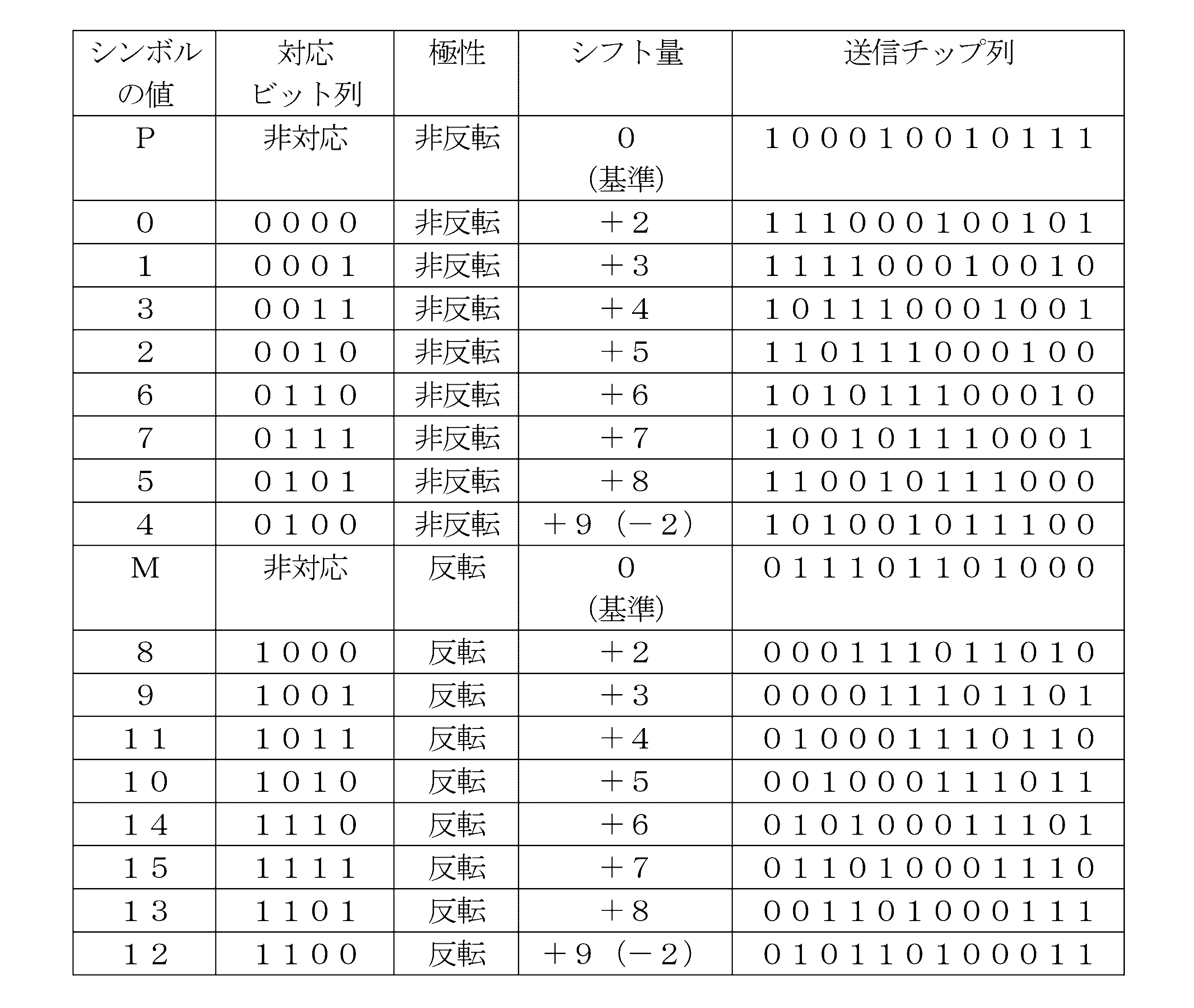
表1に示すように、この例では、まずシンボルの値「P」は、拡散符号PN「00010010111」の先頭に「1」を付けてなる送信チップ列に変換される。またシンボルの値「0」~「7」はそれぞれ、拡散符号PN「00010010111」を表1に示したシフト量で巡回シフトさせてなる符号列の先頭に「1」を付けてなる送信チップ列に変換される。その他のシンボルの値「M」「8」~「15」はそれぞれ、シンボルの値「P」「0」~「7」に対応する送信チップ列を反転させてなる送信チップ列に変換される。
As shown in Table 1, in this example, first, the symbol value “P” is converted into a transmission chip sequence in which “1” is added to the head of the spread code PN “00010010111”. Symbol values “0” to “7” are respectively transmitted to a transmission chip sequence in which “1” is added to the head of a code sequence obtained by cyclically shifting the spread code PN “00010010111” by the shift amount shown in Table 1. Converted. The other symbol values “M” “8” to “15” are converted into transmission chip sequences obtained by inverting the transmission chip sequences corresponding to the symbol values “P” “0” to “7”, respectively.
拡散処理部63は、以上のような変換処理によって送信チップ列を取得し、送信ガード部65に供給するよう構成される。
The diffusion processing unit 63 is configured to acquire the transmission chip sequence by the conversion processing as described above and supply it to the transmission guard unit 65.
送信ガード部65は、ロジック部70から供給される制御信号ctrl_t4に基づき、アップリンク信号USの送信期間と、スタイラス2からの信号を受信する受信期間との間に、送信動作と受信動作を切り替えるために送信と受信の両方を行わない期間であるガード期間を挿入する機能を有する。
Based on the control signal ctrl_t4 supplied from the logic unit 70, the transmission guard unit 65 switches between the transmission operation and the reception operation between the transmission period of the uplink signal US and the reception period for receiving the signal from the stylus 2. Therefore, it has a function of inserting a guard period, which is a period during which neither transmission nor reception is performed.
選択部40は、ロジック部70の制御に基づいて、センサ30から信号を送信する送信期間と、センサ30により信号を受信する受信期間とを切り替えるスイッチである。具体的に説明すると、選択部40は、スイッチ44x,44yと、導体選択回路41x,41yとを含んで構成される。スイッチ44xは、ロジック部70から供給される制御信号sTRxに基づき、送信期間には、送信部60の出力端を導体選択回路41xの入力端に接続し、受信期間には、導体選択回路41xの出力端を受信部50の入力端に接続するよう動作する。スイッチ44yは、ロジック部70から供給される制御信号sTRyに基づき、送信期間には、送信部60の出力端を導体選択回路41yの入力端に接続し、受信期間には、導体選択回路41yの出力端を受信部50の入力端に接続するよう動作する。導体選択回路41xは、ロジック部70から供給される制御信号selXに基づき、複数の線状電極30Xのうちの1つ又は複数を選択し、選択したものをスイッチ44xに接続するよう動作する。導体選択回路41yは、ロジック部70から供給される制御信号selYに基づき、複数の線状電極30Yのうちの1つ又は複数を選択し、選択したものをスイッチ44yに接続するよう動作する。導体選択回路41x,41yによって複数の線状電極30X又は複数の線状電極30Yが選択されるのは、例えば、タッチ面3aの全面からアップリンク信号USを送信する場合である。
The selection unit 40 is a switch that switches between a transmission period in which a signal is transmitted from the sensor 30 and a reception period in which the signal is received by the sensor 30 based on the control of the logic unit 70. More specifically, the selection unit 40 includes switches 44x and 44y and conductor selection circuits 41x and 41y. Based on the control signal sTRx supplied from the logic unit 70, the switch 44x connects the output terminal of the transmission unit 60 to the input terminal of the conductor selection circuit 41x during the transmission period, and the conductor selection circuit 41x during the reception period. It operates to connect the output end to the input end of the receiver 50. Based on the control signal sTRy supplied from the logic unit 70, the switch 44y connects the output terminal of the transmission unit 60 to the input terminal of the conductor selection circuit 41y during the transmission period, and the conductor selection circuit 41y during the reception period. It operates to connect the output end to the input end of the receiver 50. The conductor selection circuit 41x operates to select one or more of the plurality of linear electrodes 30X based on the control signal selX supplied from the logic unit 70 and connect the selected one to the switch 44x. The conductor selection circuit 41y operates to select one or more of the plurality of linear electrodes 30Y based on the control signal selY supplied from the logic unit 70 and connect the selected one to the switch 44y. The plurality of linear electrodes 30X or the plurality of linear electrodes 30Y are selected by the conductor selection circuits 41x and 41y, for example, when the uplink signal US is transmitted from the entire touch surface 3a.
受信部50は、ロジック部70の制御信号ctrl_rに基づいて、スタイラス2が送信するダウンリンク信号DS(ダウンリンク信号DS1又はダウンリンク信号DS2)を受信するための回路である。具体的には、増幅回路51、検波回路52、及び、アナログデジタル(AD)変換器53を含んで構成される。
The receiving unit 50 is a circuit for receiving the downlink signal DS (downlink signal DS1 or downlink signal DS2) transmitted by the stylus 2 based on the control signal ctrl_r of the logic unit 70. Specifically, the amplifier circuit 51 includes a detection circuit 52, a detection circuit 52, and an analog-digital (AD) converter 53.
増幅回路51は、選択部40から供給されるダウンリンク信号DSを増幅して出力する。検波回路52は、増幅回路51の出力信号のレベルに対応した電圧を生成する回路である。AD変換器53は、検波回路52から出力される電圧を所定時間間隔でサンプリングすることによって、デジタル信号を生成する回路である。AD変換器53が出力するデジタル信号は、MCU80に供給される。
The amplification circuit 51 amplifies and outputs the downlink signal DS supplied from the selection unit 40. The detection circuit 52 is a circuit that generates a voltage corresponding to the level of the output signal of the amplifier circuit 51. The AD converter 53 is a circuit that generates a digital signal by sampling the voltage output from the detection circuit 52 at predetermined time intervals. The digital signal output from the AD converter 53 is supplied to the MCU 80.
ダウンリンク信号DS1を受信できるがダウンリンク信号DS2は受信できないタイプの位置検出装置3に含まれる受信部50は、無変調のパルス列信号又はパルス列信号を変調してなる信号を受信する一方で、無変調の正弦波信号又は正弦波信号を変調してなる信号を受信しない(又は、できない)ように構成される。したがって、この場合のMCU80には、センサ30にダウンリンク信号DS1が到来した場合にのみ、受信部50からデジタル信号が供給されることになる。一方、ダウンリンク信号DS2を受信できるがダウンリンク信号DS1は受信できないタイプの位置検出装置3に含まれる受信部50は、無変調の正弦波信号又は正弦波信号を変調してなる信号を受信する一方で、無変調のパルス列信号又はパルス列信号を変調してなる信号を受信しない(又は、できない)ように構成される。したがって、この場合のMCU80には、センサ30にダウンリンク信号DS2が到来した場合にのみ、受信部50からデジタル信号が供給されることになる。
The receiving unit 50 included in the position detection device 3 of a type that can receive the downlink signal DS1 but cannot receive the downlink signal DS2 receives an unmodulated pulse train signal or a signal obtained by modulating the pulse train signal. The modulation sine wave signal or a signal obtained by modulating the sine wave signal is not received (or cannot be received). Therefore, a digital signal is supplied to the MCU 80 in this case from the receiving unit 50 only when the downlink signal DS1 arrives at the sensor 30. On the other hand, the receiving unit 50 included in the position detection device 3 of a type that can receive the downlink signal DS2 but cannot receive the downlink signal DS1 receives an unmodulated sine wave signal or a signal obtained by modulating a sine wave signal. On the other hand, an unmodulated pulse train signal or a signal obtained by modulating a pulse train signal is not received (or cannot be received). Therefore, a digital signal is supplied from the receiving unit 50 to the MCU 80 in this case only when the downlink signal DS2 arrives at the sensor 30.
ロジック部70及びMCU80は、送信部60及び受信部50等の送受信動作を制御する制御部である。具体的に説明すると、MCU80は、内部にROMおよびRAMを有し、所定のプログラムに基づき動作するマイクロプロセッサである。一方、ロジック部70は、MCU80の制御に基づき、上述した各制御信号を出力するよう構成される。MCU80はまた、AD変換器53から供給されるデジタル信号に基づいてスタイラス2の位置を示す座標データx,y等を導出し、システムコントローラ32に対して出力する処理と、AD変換器53から供給されるデジタル信号がデータ信号d1D又はデータ信号d2Dを示している場合には、そのデジタル信号により表されるデータResを取得し、システムコントローラ32に対して出力する処理とを行うよう構成される。
The logic unit 70 and the MCU 80 are control units that control transmission / reception operations of the transmission unit 60, the reception unit 50, and the like. Specifically, the MCU 80 is a microprocessor that has a ROM and a RAM therein and operates based on a predetermined program. On the other hand, the logic unit 70 is configured to output each control signal described above based on the control of the MCU 80. The MCU 80 also derives coordinate data x, y and the like indicating the position of the stylus 2 based on the digital signal supplied from the AD converter 53, outputs the coordinate data to the system controller 32, and supplies the coordinate data from the AD converter 53. When the digital signal to be displayed indicates the data signal d1D or the data signal d2D, the process is configured to perform processing for acquiring the data Res represented by the digital signal and outputting the data Res to the system controller 32.
以下、スタイラス2の構成及びスタイラス2が行う処理について詳しく説明するが、初めに、上述した交互送信方式を採用するスタイラス2について説明し、その後、本発明の第1乃至第5の実施の形態によるスタイラス2について説明することとする。
Hereinafter, the configuration of the stylus 2 and the processing performed by the stylus 2 will be described in detail. First, the stylus 2 that employs the above-described alternate transmission method will be described, and then, according to the first to fifth embodiments of the present invention. The stylus 2 will be described.
図4は、本発明の背景技術によるスタイラス2の構成を示す図である。同図に示すスタイラス2は上述した交互送信方式を採用するものであって、本発明の背景技術に相当するが、後述する第1乃至第5の実施の形態によるスタイラス2と同様に本発明の発明者が発明したものであり、本願の優先日時点で公知になっていたものではない。
FIG. 4 is a diagram showing the configuration of the stylus 2 according to the background art of the present invention. The stylus 2 shown in the figure adopts the above-described alternate transmission method and corresponds to the background art of the present invention, but the stylus 2 of the present invention is similar to the stylus 2 according to the first to fifth embodiments described later. It was invented by the inventor and was not publicly known as of the priority date of the present application.
図4に示すように、交互送信方式を採用するスタイラス2は、図1にも示した信号処理部24及び電源25に加え、増幅部26を有して構成される。信号処理部24は、制御部90a、昇圧部91、発振部92a、スイッチ部93aを有して構成される。なお、図4には、信号処理部24が有する機能のうちアップリンク信号USの受信に関する機能を示していないが、後述する本発明の各実施の形態によるスタイラス2のように、交互送信方式を採用するスタイラス2にも、アップリンク信号USの受信に関する機能を設けることは可能である。
As shown in FIG. 4, the stylus 2 that employs the alternating transmission method includes an amplification unit 26 in addition to the signal processing unit 24 and the power supply 25 shown in FIG. 1. The signal processing unit 24 includes a control unit 90a, a boosting unit 91, an oscillation unit 92a, and a switch unit 93a. 4 does not show a function related to reception of the uplink signal US among the functions of the signal processing unit 24, but an alternate transmission method is used as in the stylus 2 according to each embodiment of the present invention to be described later. The employed stylus 2 can also be provided with a function related to reception of the uplink signal US.
昇圧部91は、電源25から供給される直流電圧を昇圧することにより、直流電圧V1を生成する機能を有する。具体的な例では、昇圧部91はDC-DCコンバータ又はチャージポンプ回路によって構成される。
The booster 91 has a function of generating the DC voltage V1 by boosting the DC voltage supplied from the power supply 25. In a specific example, the booster 91 is configured by a DC-DC converter or a charge pump circuit.
発振部92aは、電源25から供給される直流電圧に基づいて発振動作を行うことにより、所定周波数で振動する無変調の正弦波信号(搬送波信号)を生成する機能を有する。増幅部26は、発振部92aによって生成された正弦波信号を所定の増幅率で増幅することにより、無変調の正弦波信号v2を生成する機能を有する。増幅部26は、図4に示すように、トランス及びキャパシタにより構成される増幅回路により構成されることが好ましい。
The oscillation unit 92a has a function of generating an unmodulated sine wave signal (carrier wave signal) that oscillates at a predetermined frequency by performing an oscillation operation based on a DC voltage supplied from the power supply 25. The amplifying unit 26 has a function of generating an unmodulated sine wave signal v2 by amplifying the sine wave signal generated by the oscillating unit 92a with a predetermined amplification factor. As shown in FIG. 4, the amplifying unit 26 is preferably configured by an amplifying circuit including a transformer and a capacitor.
スイッチ部93aは単極3投形のスイッチ素子であり、昇圧部91の出力端に接続される端子aと、増幅部26の出力端に接続される端子bと、接地電位が供給される電源配線に接続される端子gと、電極21に接続される共通端子cとを有して構成される。
The switch unit 93a is a single-pole three-throw type switch element, and includes a terminal a connected to the output terminal of the booster unit 91, a terminal b connected to the output terminal of the amplifier unit 26, and a power source to which a ground potential is supplied. A terminal g connected to the wiring and a common terminal c connected to the electrode 21 are configured.
制御部90aは、スイッチ部93aを制御するための制御信号Ctrlを供給するICであり、電源25から供給される電力により動作するよう構成される。具体的な例では、制御部90aはASIC又はMCUであってよい。
The control unit 90a is an IC that supplies a control signal Ctrl for controlling the switch unit 93a, and is configured to operate with power supplied from the power supply 25. In a specific example, the control unit 90a may be an ASIC or MCU.
ダウンリンク信号DS1を送信する場合の制御部90aは、昇圧部91の出力端と電極21の間に設けられる第1のスイッチ部として機能するよう、スイッチ部93aを制御する。つまり、端子aが共通端子cに接続されている状態と、端子gが共通端子cに接続されている状態との間で、スイッチ部93aを切り替える処理を行う。端子aが共通端子cに接続されている状態は第1のスイッチ部がオンとなっている状態に対応し、端子gが共通端子cに接続されている状態は第1のスイッチ部がオフとなっている状態に対応する。
When transmitting the downlink signal DS1, the control unit 90a controls the switch unit 93a so as to function as a first switch unit provided between the output terminal of the booster unit 91 and the electrode 21. That is, a process of switching the switch unit 93a between a state where the terminal a is connected to the common terminal c and a state where the terminal g is connected to the common terminal c is performed. The state in which the terminal a is connected to the common terminal c corresponds to the state in which the first switch unit is on, and the state in which the terminal g is connected to the common terminal c is that the first switch unit is off. Corresponds to the state.
ダウンリンク信号DS1のうちバースト信号d1Bを送信するタイミングでは、制御部90aは、所定の周期で周期的にスイッチ部93aの切り替え制御を行う。端子aが共通端子cに接続されている場合には、直流電圧V1がスイッチ部93aの出力電圧となる。一方、端子gが共通端子cに接続されている場合には、接地電位がスイッチ部93aの出力電圧となる。したがって、スイッチ部93aからは無変調のパルス列信号が出力され、これがバースト信号d1Bとなる。
At the timing of transmitting the burst signal d1B in the downlink signal DS1, the control unit 90a performs switching control of the switch unit 93a periodically at a predetermined cycle. When the terminal a is connected to the common terminal c, the DC voltage V1 becomes the output voltage of the switch section 93a. On the other hand, when the terminal g is connected to the common terminal c, the ground potential becomes the output voltage of the switch section 93a. Therefore, an unmodulated pulse train signal is output from the switch section 93a, and this becomes the burst signal d1B.
一方、ダウンリンク信号DS1のうちデータ信号d1Dを送信するタイミングでは、制御部90aは、筆圧レベルPやスイッチ情報SWなどのデータResに応じてスイッチ部93aの切り替え制御を行う。なお、データResには、スタイラス2の識別情報などの他の情報を含んでもよい。制御部90aは、この切り替え制御によって、データResに基づいて変調されたパルス列信号であるデータ信号d1Dを生成する。
On the other hand, at the timing of transmitting the data signal d1D in the downlink signal DS1, the control unit 90a performs switching control of the switch unit 93a according to the data Res such as the writing pressure level P and the switch information SW. The data Res may include other information such as identification information of the stylus 2. The control unit 90a generates a data signal d1D that is a pulse train signal modulated based on the data Res by this switching control.
制御部90aによるパルス列信号の変調の具体的な方式としては、多種のものが考えられる。以下では、オンオフ変調を用いる場合と、周波数変調を用いる場合とについて、具体的な例を示して説明する。
As the specific method of modulating the pulse train signal by the control unit 90a, various methods are conceivable. Hereinafter, a specific example will be described for the case where on-off modulation is used and the case where frequency modulation is used.
図5は、制御部90aにより生成されるデータ信号d1Dの一例(オンオフ変調されたパルス列信号である場合)を示す図である。この場合の制御部90aは、データResの送信対象ビットが「1」である場合にスイッチ部93aを端子a側に切り替え、データResの送信対象ビットが「0」である場合にスイッチ部93bを端子g側に切り替える。これによりデータ信号d1Dは、図5に示すように、送信対象ビットが「1」である場合にハイレベル(=直流電圧V1)となり、送信対象ビットが「0」である場合にローレベル(=接地電位)となる2値信号となる。
FIG. 5 is a diagram illustrating an example of the data signal d1D generated by the control unit 90a (in the case of an on / off modulated pulse train signal). In this case, the control unit 90a switches the switch unit 93a to the terminal a side when the transmission target bit of the data Res is “1”, and switches the switch unit 93b when the transmission target bit of the data Res is “0”. Switch to terminal g side. As a result, as shown in FIG. 5, the data signal d1D becomes high level (= DC voltage V1) when the transmission target bit is “1”, and low level (== when the transmission target bit is “0”. (A ground potential).
図6は、制御部90aにより生成されるデータ信号d1Dの他の一例(周波数変調されたパルス列信号である場合)を示す図である。この場合の制御部90aは、データResの値に応じた周波数でスイッチ部93bの切り替え制御を行う。例えば図6には、データResが8ビットのデータであり、この8ビットのデータにより表される値がxである場合に、制御部90aが周波数N-x×m[Hz]でスイッチ部93bの切り替え制御を行う例を示している。この例に示すように、この場合のデータ信号d1Dは、データResの値に応じた周波数で振動するパルス列信号となる。
FIG. 6 is a diagram showing another example of the data signal d1D generated by the control unit 90a (in the case of a frequency-modulated pulse train signal). In this case, the control unit 90a performs switching control of the switch unit 93b at a frequency corresponding to the value of the data Res. For example, in FIG. 6, when the data Res is 8-bit data and the value represented by the 8-bit data is x, the control unit 90 a uses the frequency N−x × m [Hz] and the switch unit 93 b The example which performs switching control of is shown. As shown in this example, the data signal d1D in this case is a pulse train signal that vibrates at a frequency corresponding to the value of the data Res.
図4に戻り、ダウンリンク信号DS2を送信する場合の制御部90aは、増幅部26の出力端と電極21の間に設けられる第2のスイッチ部として機能するよう、スイッチ部93aを制御する。つまり、端子bが共通端子cに接続されている状態と、端子gが共通端子cに接続されている状態との間で、スイッチ部93aを切り替える処理を行う。端子bが共通端子cに接続されている状態は第2のスイッチ部がオンとなっている状態に対応し、端子gが共通端子cに接続されている状態は第2のスイッチ部がオフとなっている状態に対応する。
4, the control unit 90a in the case of transmitting the downlink signal DS2 controls the switch unit 93a so as to function as a second switch unit provided between the output terminal of the amplification unit 26 and the electrode 21. That is, a process of switching the switch unit 93a between a state where the terminal b is connected to the common terminal c and a state where the terminal g is connected to the common terminal c is performed. The state in which the terminal b is connected to the common terminal c corresponds to the state in which the second switch unit is on, and the state in which the terminal g is connected to the common terminal c is that the second switch unit is off. Corresponds to the state.
ダウンリンク信号DS2のうちバースト信号d2Bを送信するタイミングでは、制御部90aは、スイッチ部93aを端子b側に固定する。したがって、スイッチ部93aからは無変調の正弦波信号v2が出力され、これがバースト信号d2Bとなる。
At the timing of transmitting the burst signal d2B in the downlink signal DS2, the control unit 90a fixes the switch unit 93a to the terminal b side. Therefore, an unmodulated sine wave signal v2 is output from the switch section 93a, which becomes a burst signal d2B.
一方、ダウンリンク信号DS2のうちデータ信号d2Dを送信するタイミングでは、制御部90aは、筆圧レベルPやスイッチ情報SWなどのデータResに基づいてスイッチ部93aの切り替え制御を行う。なお、この場合においても、データResにはスタイラス2の識別情報などの他の情報を含んでもよい。制御部90aは、この切り替え制御によって、データResに基づいて変調された正弦波信号であるデータ信号d2Dを生成する。
On the other hand, at the timing of transmitting the data signal d2D of the downlink signal DS2, the control unit 90a performs switching control of the switch unit 93a based on the data Res such as the writing pressure level P and the switch information SW. Even in this case, the data Res may include other information such as identification information of the stylus 2. The control unit 90a generates a data signal d2D, which is a sine wave signal modulated based on the data Res, by this switching control.
制御部90aによる正弦波信号の変調の具体的な方式としては、オンオフ変調が採用される。
On-off modulation is adopted as a specific method of modulating the sine wave signal by the control unit 90a.
図7は、制御部90aにより生成されるデータ信号d2Dの一例(オンオフ変調された正弦波信号である場合)を示す図である。制御部90aは、データResの送信対象ビットが「1」である場合にスイッチ部93aを端子b側に切り替え、データResの送信対象ビットが「0」である場合にスイッチ部93bを端子g側に切り替える。これによりデータ信号d2Dは、図7に示すように、送信対象ビットが「1」である場合に正弦波信号v2となり、送信対象ビットが「0」である場合に接地電位に固定される信号となる。
FIG. 7 is a diagram illustrating an example of the data signal d2D generated by the control unit 90a (in the case of a sine wave signal subjected to on / off modulation). The control unit 90a switches the switch unit 93a to the terminal b side when the transmission target bit of the data Res is “1”, and switches the switch unit 93b to the terminal g side when the transmission target bit of the data Res is “0”. Switch to. As a result, as shown in FIG. 7, the data signal d2D becomes a sine wave signal v2 when the transmission target bit is “1”, and is fixed to the ground potential when the transmission target bit is “0”. Become.
ここで、図7から理解されるように、送信対象ビットが「0」である場合には、何も送信していないのと同じ状態となる。この何も送信していない状態が継続するのを防止するため、制御部90aは、データResをまずマンチェスター符号化し、マンチェスター符号化したデータResに基づいてスイッチ部93aの切り替え制御を行うことにより、データ信号d2Dを生成することとしてもよい。
Here, as understood from FIG. 7, when the transmission target bit is “0”, the state is the same as when nothing is transmitted. In order to prevent the state in which nothing is transmitted from continuing, the control unit 90a first performs the Manchester encoding of the data Res, and performs the switching control of the switch unit 93a based on the Manchester encoded data Res. The data signal d2D may be generated.
図4に戻り、制御部90aは、ダウンリンク信号DS1と、ダウンリンク信号DS2とを交互に送信するように構成される。これは、ダウンリンク信号DS1のみに対応する位置検出装置3と、ダウンリンク信号DS2のみに対応する位置検出装置3とのいずれにもスタイラス2の送信信号を受信させることができるようにするためであり、ダウンリンク信号DS1,DS2を交互に送信することから、本願の発明者は「交互送信方式」と呼んでいる。以下、具体的に説明する。
Referring back to FIG. 4, the control unit 90a is configured to alternately transmit the downlink signal DS1 and the downlink signal DS2. This is so that both the position detection device 3 corresponding only to the downlink signal DS1 and the position detection device 3 corresponding only to the downlink signal DS2 can receive the transmission signal of the stylus 2. Since the downlink signals DS1 and DS2 are alternately transmitted, the inventor of the present application calls the “alternate transmission method”. This will be specifically described below.
図8は、制御部90aが行う処理を示すフロー図である。また、図9は、制御部90aにより生成される信号の一例を示す図である。なお、図9の横軸は時間を示し、横軸の上側は送信Txを下側は受信Rxを示している。以下、これらの図を参照しながら説明を続ける。
FIG. 8 is a flowchart showing processing performed by the control unit 90a. FIG. 9 is a diagram illustrating an example of a signal generated by the control unit 90a. In FIG. 9, the horizontal axis indicates time, the upper side of the horizontal axis indicates transmission Tx, and the lower side indicates reception Rx. Hereinafter, the description will be continued with reference to these drawings.
まず図9に示すように、制御部90aは、一定の周期T1で、ダウンリンク信号DS1,DS2の送信処理を繰り返すよう構成される。各周期T1の中において制御部90aは、ダウンリンク信号DS1のバースト信号d1B、ダウンリンク信号DS1のデータ信号d1D、ダウンリンク信号DS2のバースト信号d2B、ダウンリンク信号DS2のデータ信号d2Dの順に、各信号の送信処理を行う。ダウンリンク信号DS1の送信は周期T1中d1(d1<T1)の時間を用いて実行され、ダウンリンク信号DS2の送信は周期T1中d2(d2=T1-d1)の時間を用いて実行される。なお、一般的にはd1<d2となる。
First, as shown in FIG. 9, the control unit 90a is configured to repeat the transmission processing of the downlink signals DS1 and DS2 at a constant period T1. In each cycle T1, the control unit 90a performs each of the burst signal d1B of the downlink signal DS1, the data signal d1D of the downlink signal DS1, the burst signal d2B of the downlink signal DS2, and the data signal d2D of the downlink signal DS2. Perform signal transmission processing. The transmission of the downlink signal DS1 is performed using the time d1 (d1 <T1) during the period T1, and the transmission of the downlink signal DS2 is performed using the time d2 (d2 = T1-d1) during the period T1. . In general, d1 <d2.
ここで、T1及びd2の具体的な値は、制御部90aによるダウンリンク信号DS2の送信周期が、ダウンリンク信号DS2の送信のみに対応するスタイラス(すなわち、ダウンリンク信号DS1の送信機能を有しないスタイラス)によるダウンリンク信号DS2の送信周期に等しくなるよう選択することが好適である。こうすることで、センサコントローラ31側では、ダウンリンク信号DS2の送信のみに対応するスタイラスが送信する場合と同様の周期で、ダウンリンク信号DS2を受信することが可能になる。なお、ダウンリンク信号DS2の送信のみに対応するスタイラス同じデータ量のダウンリンク信号DS2を送信しようとすると、ダウンリンク信号DS1の送信を行う必要があるために時間が足りなくなることも考えられるが、その場合には、バースト信号d2B及びデータ信号d2Dの一方又は両方について、送信データ量を低減しても構わない。例えば、ダウンリンク信号DS2の送信のみに対応するスタイラスが一回の周期でN個のシンボルを送信するとして、制御部90aは、周期T1の一周期内にM個(M<N)のシンボルのみを送信することとしてもよい。
Here, specific values of T1 and d2 indicate that the transmission period of the downlink signal DS2 by the control unit 90a is a stylus corresponding to only the transmission of the downlink signal DS2 (that is, does not have a transmission function of the downlink signal DS1). It is preferable to select to be equal to the transmission cycle of the downlink signal DS2 by the stylus. By doing so, on the sensor controller 31 side, it is possible to receive the downlink signal DS2 in the same cycle as when a stylus corresponding only to the transmission of the downlink signal DS2 transmits. Note that, if it is attempted to transmit the downlink signal DS2 having the same data amount as that of the stylus corresponding to only the transmission of the downlink signal DS2, it may be necessary to transmit the downlink signal DS1, and time may be insufficient. In that case, the transmission data amount may be reduced for one or both of the burst signal d2B and the data signal d2D. For example, assuming that the stylus corresponding only to the transmission of the downlink signal DS2 transmits N symbols in one cycle, the control unit 90a has only M (M <N) symbols in one cycle of the cycle T1. May be transmitted.
また、図9において水玉でハッチングした区間は、正弦波信号v2が送信されている区間を表している。この表記によれば、同図に示すように、データ信号d2Dは断続的に送信される信号となる。これは、図7を参照して説明したように、送信対象ビットが「0」である場合に信号処理部24が正弦波信号v2を出力しないことに対応するものである。
Further, the section hatched with polka dots in FIG. 9 represents the section in which the sine wave signal v2 is transmitted. According to this notation, as shown in the figure, the data signal d2D is an intermittently transmitted signal. As described with reference to FIG. 7, this corresponds to the fact that the signal processing unit 24 does not output the sine wave signal v <b> 2 when the transmission target bit is “0”.
図8のフロー図を参照すると、制御部90aは、処理を開始するとまず、ダウンリンク信号DS1の送信を開始する(ステップS1)。その後、ダウンリンク信号DS1の送信を行いつつ時間の経過を監視し(ステップS2)、所定時間d1が経過すると、ダウンリンク信号DS2の送信を開始する(ステップS3)。その後、ダウンリンク信号DS2の送信を行いつつ時間の経過を監視し(ステップS4)、所定時間d2が経過すると、ステップS1に戻って再びダウンリンク信号DS1の送信を開始する。このように、制御部90aは、ダウンリンク信号DS1,DS2の送信を交互に行う。これにより、ダウンリンク信号DS1のみに対応する位置検出装置3と、ダウンリンク信号DS2のみに対応する位置検出装置3とのいずれにも、スタイラス2の送信信号を受信させることが可能になる。
Referring to the flowchart of FIG. 8, when starting the processing, the control unit 90a first starts transmitting the downlink signal DS1 (step S1). Thereafter, the passage of time is monitored while transmitting the downlink signal DS1 (step S2), and when the predetermined time d1 has elapsed, transmission of the downlink signal DS2 is started (step S3). Thereafter, the elapse of time is monitored while transmitting the downlink signal DS2 (step S4), and when the predetermined time d2 elapses, the process returns to step S1 and starts transmitting the downlink signal DS1 again. In this way, the control unit 90a alternately transmits the downlink signals DS1 and DS2. As a result, it is possible for both the position detection device 3 corresponding to only the downlink signal DS1 and the position detection device 3 corresponding to only the downlink signal DS2 to receive the transmission signal of the stylus 2.
一方で、制御部90aの制御によれば、常に、ダウンリンク信号DS1,DS2の両方が繰り返し送信されることになる。これではダウンリンク信号DS1,DS2のいずれか一方が常に無駄に送信されていることになるので、上述したように、スタイラス2の低消費電力化の観点から好ましくない。本発明は交互送信方式のこのような課題に着目したもので、交互送信方式よりも低消費電力で、位置検出装置3を移るたびにスタイラスを持ち替えなくて済むようにすることを実現する。以下、本発明の第1乃至第5の実施の形態について、順に詳しく説明する。
On the other hand, according to the control of the control unit 90a, both the downlink signals DS1 and DS2 are always transmitted repeatedly. In this case, one of the downlink signals DS1 and DS2 is always transmitted in vain, which is not preferable from the viewpoint of reducing the power consumption of the stylus 2 as described above. The present invention pays attention to such a problem of the alternate transmission method, and achieves lower power consumption than the alternate transmission method and does not have to change the stylus every time the position detecting device 3 is moved. Hereinafter, first to fifth embodiments of the present invention will be described in detail.
図10は、本発明の第1の実施の形態によるスタイラス2の構成を示す図である。同図に示すスタイラス2は、制御部90a及びスイッチ部93aに代えて制御部90b及びスイッチ部93bを有する点で、図4に示したスタイラス2と相違する。その他の点では図4に示したスタイラス2と同様であるので、同一の構成には同一の符号を付し、以下では相違点に着目して説明する。
FIG. 10 is a diagram showing the configuration of the stylus 2 according to the first embodiment of the present invention. The stylus 2 shown in the figure is different from the stylus 2 shown in FIG. 4 in that a control unit 90b and a switch unit 93b are provided instead of the control unit 90a and the switch unit 93a. Since the other points are the same as those of the stylus 2 shown in FIG. 4, the same components are denoted by the same reference numerals, and the following description will be made paying attention to different points.
スイッチ部93bは、スイッチ部93aに端子rを追加し、単極4投形としたものである。端子rは、バッファを経て、制御部90bの受信端子に接続される。また、制御部90bは、アップリンク信号USの受信機能を制御部90aに追加した他、第1及び第2のモードのいずれか一方で動作するよう構成したものである。
The switch unit 93b is a single-pole four-throw type by adding a terminal r to the switch unit 93a. The terminal r is connected to the receiving terminal of the control unit 90b via a buffer. The control unit 90b is configured to operate in one of the first and second modes, in addition to the reception function of the uplink signal US added to the control unit 90a.
アップリンク信号USの受信機能に関して、制御部90bは、送信と受信を時分割で行うよう構成される。すなわち、制御部90bは、送信と受信を同時に行えるようには構成されていない。送信のための制御部90bの基本的な動作は、制御部90aについて上述した通りである。一方、受信を行う際には、制御部90bは、制御信号Ctrlによってスイッチ部93bを端子r側に切り替える。これにより、電極21に現れた電荷が制御部90bの受信端子に供給されるので、制御部90bは、こうして供給された電荷に基づいて、位置検出装置3が送信したアップリンク信号USを受信する。
Regarding the reception function of the uplink signal US, the control unit 90b is configured to perform transmission and reception in a time division manner. That is, the control unit 90b is not configured to perform transmission and reception at the same time. The basic operation of the control unit 90b for transmission is as described above for the control unit 90a. On the other hand, when receiving, the control unit 90b switches the switch unit 93b to the terminal r side by the control signal Ctrl. As a result, the charge appearing on the electrode 21 is supplied to the reception terminal of the control unit 90b, and the control unit 90b receives the uplink signal US transmitted by the position detection device 3 based on the supplied charge. .
第1のモードは、スタイラス2がダウンリンク信号DS1を送信するモードである。一方、第2のモードは、スタイラス2がダウンリンク信号DS2を送信するモードである。制御部90bは、第1のモードでの動作中に、上述した処理によりダウンリンク信号DS1を生成して電極21に供給する一方、第2のモードへの切り替えの要否を判定する処理を行う。一方、第2のモードでの動作中には、上述した処理によりダウンリンク信号DS2を生成して電極21に供給する一方、第1のモードへの切り替えの要否を判定する処理を行う。制御部90bは、これらの判定を、各モードにおけるアップリンク信号USの受信の有無に基づいて行う。そして、判定の結果として第2のモードへの切り替えが必要であると判定した場合には、自身の動作を第2のモードでの動作に切り替える。また、第1のモードへの切り替えが必要であると判定した場合には、自身の動作を第1のモードでの動作に切り替える。以下、具体的に説明する。
The first mode is a mode in which the stylus 2 transmits the downlink signal DS1. On the other hand, the second mode is a mode in which the stylus 2 transmits the downlink signal DS2. During the operation in the first mode, the control unit 90b generates the downlink signal DS1 by the above-described process and supplies the downlink signal DS1 to the electrode 21, while performing a process for determining whether or not it is necessary to switch to the second mode. . On the other hand, during the operation in the second mode, the downlink signal DS2 is generated and supplied to the electrode 21 by the above-described processing, and processing for determining whether or not switching to the first mode is necessary is performed. The controller 90b makes these determinations based on whether or not the uplink signal US is received in each mode. If it is determined that the switching to the second mode is necessary as a result of the determination, the own operation is switched to the operation in the second mode. Further, when it is determined that switching to the first mode is necessary, its own operation is switched to the operation in the first mode. This will be specifically described below.
図11~図13は、制御部90bが行う処理を示すフロー図である。また、図14は、制御部90bにより生成される信号の一例を示す図である。なお、図14の横軸は時間を示し、横軸の上側は送信Txを下側は受信Rxを示している。以下、これらの図を参照しながら説明を続ける。
11 to 13 are flowcharts showing processing performed by the control unit 90b. FIG. 14 is a diagram illustrating an example of a signal generated by the control unit 90b. In FIG. 14, the horizontal axis indicates time, the upper side of the horizontal axis indicates transmission Tx, and the lower side indicates reception Rx. Hereinafter, the description will be continued with reference to these drawings.
まず図14に示すように、制御部90bは、図9にも示した一定の周期T1(所定の第1の周期)で、ダウンリンク信号DS1を間欠的に送信するよう構成される。これは、第1のモードでの動作である。より具体的に言えば、制御部90bは、各周期T1の始期から周期T1より短い所定時間d1にわたり、ダウンリンク信号DS1を送信するよう構成される。このようにダウンリンク信号DS1が間欠的に送信されているため、周期T1内には、送信動作を行っていない期間が必ず存在する。制御部90bは、この期間を利用し、電極21を用いて位置検出装置3が送信したアップリンク信号USの検出動作を行う。そして、その検出結果に応じて、第2のモードへの切り替えの要否を判定する。したがって、制御部90bは、周期T1で、第2のモードへの切り替えの要否を判定していることになる。
First, as shown in FIG. 14, the controller 90b is configured to intermittently transmit the downlink signal DS1 at a constant cycle T1 (predetermined first cycle) also shown in FIG. This is the operation in the first mode. More specifically, the control unit 90b is configured to transmit the downlink signal DS1 over a predetermined time d1 shorter than the period T1 from the beginning of each period T1. Since the downlink signal DS1 is transmitted intermittently in this way, there is always a period during which no transmission operation is performed in the period T1. Using this period, the controller 90b performs an operation of detecting the uplink signal US transmitted from the position detection device 3 using the electrode 21. Then, the necessity of switching to the second mode is determined according to the detection result. Therefore, the control unit 90b determines whether or not it is necessary to switch to the second mode at the cycle T1.
第2のモードに切り替わった後の制御部90bは、一定の周期d2(所定の第2の周期)で、ダウンリンク信号DS2を間欠的に送信するよう構成される。なお、この周期d2の時間長は、図9に示した所定時間d2と等しくてもよいし、等しくなくてもよい。この間欠的な送信は、上述したように、データ信号d2Dの送信の際、送信対象ビットが「1」である場合には信号処理部24から正弦波信号v2が出力される一方、送信対象ビットが「0」である場合には信号処理部24から正弦波信号v2が出力されないことによって実現されるものである。したがって、ダウンリンク信号DS2の間欠的な送信は、図14にも示すように、バースト信号d2Bではなくデータ信号d2Dの送信中に行われる。制御部90bは、この間欠的な送信によって信号処理部24から正弦波信号v2が出力されていない期間を利用し、電極21を用いて位置検出装置3が送信したアップリンク信号USの検出動作を行う。そして、検出の結果に応じて、周期d2ごとに、第1のモードへの切り替えの要否を判定する。
The controller 90b after switching to the second mode is configured to intermittently transmit the downlink signal DS2 at a constant period d2 (predetermined second period). The time length of the period d2 may or may not be equal to the predetermined time d2 shown in FIG. As described above, in the intermittent transmission, when the transmission target bit is “1” when the data signal d2D is transmitted, the signal processing unit 24 outputs the sine wave signal v2, while the transmission target bit. Is “0”, this is realized by not outputting the sine wave signal v 2 from the signal processing unit 24. Therefore, intermittent transmission of the downlink signal DS2 is performed during transmission of the data signal d2D instead of the burst signal d2B, as shown in FIG. The control unit 90b uses the period in which the sine wave signal v2 is not output from the signal processing unit 24 due to the intermittent transmission, and performs the detection operation of the uplink signal US transmitted by the position detection device 3 using the electrode 21. Do. Then, it is determined whether or not it is necessary to switch to the first mode for each cycle d2 according to the detection result.
図11のフロー図を参照すると、制御部90bは、第1のモードでの動作を行うサブルーチン(ステップS10)と、第2のモードでの動作を行うサブルーチン(ステップS30)とを交互に実行するよう構成される。詳しくは図12及び図13を参照しながら説明するが、この処理は、ステップS10とステップS30の切り替えが時間の経過に応じて行われるわけではなく、各サブルーチンの中で実行されるモード切り替え要否の判定処理の結果に基づいて行われる点で、図8に示した制御部90aの処理と異なっている。以下、ステップS10,S30のそれぞれにおける処理について、詳しく説明する。
Referring to the flowchart of FIG. 11, the control unit 90b alternately executes a subroutine (step S10) for performing the operation in the first mode and a subroutine (step S30) for performing the operation in the second mode. It is configured as follows. Although details will be described with reference to FIGS. 12 and 13, this process does not necessarily switch between step S <b> 10 and step S <b> 30 according to the passage of time, but requires mode switching to be executed in each subroutine. This is different from the process of the control unit 90a shown in FIG. 8 in that it is performed based on the result of the determination process of NO. Hereinafter, the processing in each of steps S10 and S30 will be described in detail.
図12は、第1のモードでの動作(図11に示すステップS10)の詳細を示すフロー図である。同図に示すように、第1のモードで動作中の制御部90bはまず、ダウンリンク信号DS1(バースト信号d1B及びデータ信号d1Dを含む)の送信を開始する(ステップS11)。その後、ダウンリンク信号DS1の送信を行いつつ時間の経過を監視し(ステップS12)、所定時間d1が経過すると、アップリンク信号USの受信を開始する(ステップS13)。そして、所定時間dr(dr≦T1-d1)が経過すると(ステップS14)、アップリンク信号USの受信を終了し(ステップS15)、所定の周期T1の経過を待って(ステップS16)、第1のモードを維持するか否かを判定する(ステップS17)。
FIG. 12 is a flowchart showing details of the operation in the first mode (step S10 shown in FIG. 11). As shown in the figure, the control unit 90b operating in the first mode starts transmission of the downlink signal DS1 (including the burst signal d1B and the data signal d1D) (step S11). Thereafter, the passage of time is monitored while transmitting the downlink signal DS1 (step S12), and when the predetermined time d1 has elapsed, reception of the uplink signal US is started (step S13). Then, when the predetermined time dr (dr ≦ T1-d1) has elapsed (step S14), the reception of the uplink signal US is terminated (step S15), and after the predetermined period T1 has elapsed (step S16), the first It is determined whether or not to maintain this mode (step S17).
ここで、上述したように、アップリンク信号USを送信する能力を有するのはダウンリンク信号DS2を受信できるタイプの位置検出装置3のみであって、ダウンリンク信号DS2を受信できないタイプの位置検出装置3はアップリンク信号USの送信機能を有しない。したがって、アップリンク信号USが受信されているということは、ダウンリンク信号DS2を受信できる位置検出装置3がスタイラス2の近くに存在していることを意味する。そこで、ステップS17において制御部90bは、今回のサブルーチン実行の間(より具体的には、ステップS13でアップリンク信号USの受信を開始してからステップS15でアップリンク信号USの受信を終了するまでの間)にアップリンク信号USが受信されていた場合に、スタイラス2がダウンリンク信号DS2を送信できるようにするため、第1のモードを維持しない(すなわち、第2のモードに切り替える)と判定する。逆に、今回のサブルーチン実行の間にアップリンク信号USが受信されていない場合には、ダウンリンク信号DS2を受信できる位置検出装置3はスタイラス2の近くに存在しないと判断し、第1のモードを維持する(すなわち、第2のモードに切り替えない)と判定する。
Here, as described above, only the position detection device 3 of the type capable of receiving the downlink signal DS2 has the ability to transmit the uplink signal US, and the type of position detection device of the type not capable of receiving the downlink signal DS2. 3 does not have a function of transmitting the uplink signal US. Therefore, the fact that the uplink signal US is received means that the position detecting device 3 that can receive the downlink signal DS2 exists near the stylus 2. Therefore, in step S17, the control unit 90b performs the current subroutine execution (more specifically, from the start of reception of the uplink signal US in step S13 to the end of reception of the uplink signal US in step S15). In the case that the uplink signal US is received during (between), the stylus 2 determines that the first mode is not maintained (that is, switched to the second mode) so that the stylus 2 can transmit the downlink signal DS2. To do. On the contrary, if the uplink signal US is not received during the current subroutine execution, it is determined that the position detection device 3 that can receive the downlink signal DS2 does not exist near the stylus 2, and the first mode Is maintained (that is, it is not switched to the second mode).
ステップS17で第1のモードを維持すると判定した場合、制御部90bは、ステップS11に戻って処理を続ける。すなわち、図11に示したステップS10のサブルーチン(図12に示す第1のモードでの動作)が繰り返される。一方、ステップS17で第1のモードを維持しないと判定した場合、制御部90bは、ステップS10のサブルーチンを抜けて処理を続ける。これにより、図11に示したステップS30のサブルーチン(図13に示す第2のモードでの動作)が開始されることになる。
When it determines with maintaining a 1st mode by step S17, the control part 90b returns to step S11 and continues a process. That is, the subroutine of step S10 shown in FIG. 11 (operation in the first mode shown in FIG. 12) is repeated. On the other hand, when it is determined in step S17 that the first mode is not maintained, the control unit 90b exits the subroutine of step S10 and continues the process. Thereby, the subroutine of step S30 shown in FIG. 11 (operation in the second mode shown in FIG. 13) is started.
図13は、第2のモードでの動作(図11に示すステップS30)の詳細を示すフロー図である。同図に示すように、第2のモードで動作中の制御部90bはまず、バースト信号d2Bの送信を開始する(ステップS31)。バースト信号d2Bの送信時間は予め決められており、次いで制御部90bは、この予め決められた送信時間が満了したか否かを判定することにより、バースト信号d2Bの送信が終了したか否かを判定する(ステップS32)。
FIG. 13 is a flowchart showing details of the operation in the second mode (step S30 shown in FIG. 11). As shown in the figure, the control unit 90b operating in the second mode first starts transmitting the burst signal d2B (step S31). The transmission time of the burst signal d2B is determined in advance, and then the control unit 90b determines whether or not the transmission of the burst signal d2B is completed by determining whether or not the predetermined transmission time has expired. Determination is made (step S32).
次に、制御部90bは、データ信号d2Dを構成する各送信対象ビット(データResの各ビット。ただし、マンチェスター符号化を行う場合には、マンチェスター符号化したデータResの各ビット)を順次対象とするループ処理を行う(ステップS33)。このループ処理は、周期d2が経過するまでの間、繰り返される(ステップS38)。
Next, the control unit 90b sequentially targets each transmission target bit (each bit of the data Res. Each bit of the Manchester encoded data Res when performing the Manchester encoding) constituting the data signal d2D. A loop process is performed (step S33). This loop process is repeated until the period d2 elapses (step S38).
ステップS33のループ処理において制御部90bはまず、送信対象ビットが「1」であるか否かを判定する(ステップS34)。この処理では、送信対象ビットが「0」である場合に否定判定がなされる。なお、送信対象のデータResが存在しない場合におけるステップS34の判定結果は、送信対象ビットが「0」である場合と同じく否定とすればよい。
In the loop process of step S33, the control unit 90b first determines whether or not the transmission target bit is “1” (step S34). In this process, a negative determination is made when the transmission target bit is “0”. Note that the determination result in step S <b> 34 when there is no transmission target data Res may be negative as in the case where the transmission target bit is “0”.
ステップS34で否定的な結果が得られた場合、制御部90bは、アップリンク信号USの受信を開始する(ステップS35)。一方、ステップS34で肯定的な結果が得られた場合、制御部90bは、アップリンク信号USの受信動作を行っていた場合にはアップリンク信号USの受信動作を終了したうえで(ステップS36)、1ビット分の正弦波信号v2の送信を開始する(ステップS37)。
If a negative result is obtained in step S34, the control unit 90b starts receiving the uplink signal US (step S35). On the other hand, when a positive result is obtained in step S34, the control unit 90b ends the reception operation of the uplink signal US when the reception operation of the uplink signal US is performed (step S36). Transmission of the 1-bit sine wave signal v2 is started (step S37).
ステップS35でアップリンク信号USの受信を開始した後、又は、ステップS37で正弦波信号v2の送信を開始した後、制御部90bは、周期d2が経過したか否かを判定する(ステップS38)。そして、経過していないと判定した場合にはステップS34に戻り、次の送信対象ビットを対象として処理を繰り返す。一方、ステップS38で経過したと判定した場合には、ループ処理を抜けて第2のモードを維持するか否かの判定を行う(ステップS39)。
After starting the reception of the uplink signal US in step S35 or starting the transmission of the sine wave signal v2 in step S37, the control unit 90b determines whether or not the period d2 has elapsed (step S38). . If it is determined that it has not elapsed, the process returns to step S34, and the process is repeated for the next transmission target bit. On the other hand, if it is determined in step S38 that the time has elapsed, it is determined whether or not the second mode is maintained by exiting the loop process (step S39).
ステップS39の判定の基準は、図12に示したステップS17における判定の基準と同様とすることが好ましい。すなわち、制御部90bは、今回のサブルーチン実行の間(より具体的には、ステップS35でアップリンク信号USの受信を開始してからステップS36でアップリンク信号USの受信を終了するまでの間。第2のモードでは、この期間が複数回存在する)にアップリンク信号USが受信されていた場合には、第2のモードを維持する(すなわち、第1のモードに切り替えない)と判定し、逆に、今回のサブルーチン実行の間にアップリンク信号USが受信されていない場合には、第2のモードを維持しない(すなわち、第1のモードに切り替える)と判定することが好ましい。
It is preferable that the determination criterion in step S39 is the same as the determination criterion in step S17 shown in FIG. That is, the control unit 90b performs the current subroutine (more specifically, from the start of reception of the uplink signal US in step S35 to the end of reception of the uplink signal US in step S36). In the second mode, when the uplink signal US has been received in the period of time multiple times), it is determined to maintain the second mode (that is, do not switch to the first mode), Conversely, when the uplink signal US is not received during the current subroutine execution, it is preferable to determine that the second mode is not maintained (that is, the mode is switched to the first mode).
ステップS39で第2のモードを維持すると判定した場合、制御部90bは、ステップS31に戻って処理を続ける。これにより、図11に示したステップS30のサブルーチン(図13に示す第2のモードでの動作)が繰り返される。一方、ステップS39で第2のモードを維持しないと判定した場合、制御部90bは、ステップS30のサブルーチンを抜けて処理を続ける。これにより、図11に示したステップS10のサブルーチン(図12に示す第1のモードでの動作)が開始されることになる。
When it determines with maintaining a 2nd mode by step S39, the control part 90b returns to step S31 and continues a process. Thereby, the subroutine of step S30 shown in FIG. 11 (operation in the second mode shown in FIG. 13) is repeated. On the other hand, when it is determined in step S39 that the second mode is not maintained, the control unit 90b exits the subroutine of step S30 and continues the process. Thereby, the subroutine of step S10 shown in FIG. 11 (operation in the first mode shown in FIG. 12) is started.
以上説明したように、本実施の形態によるスタイラス2の構成及び動作によれば、スタイラス2側でモード切り替えの要否を判定し、その結果に応じてスタイラス2自身の動作モードを切り替えているので、スタイラス2の動作モードを、ダウンリンク信号DS1の受信のみに対応する位置検出装置3とともに使用する場合には第1のモードとし、ダウンリンク信号DS2の受信のみに対応する位置検出装置3とともに使用する場合には第2のモードとすることができる。したがって、ダウンリンク信号DS1の受信のみに対応する位置検出装置3(上述した第1の方式のみに対応する位置検出装置)とともに使用する場合にはダウンリンク信号DS2を送信せず、ダウンリンク信号DS2の受信のみに対応する位置検出装置3(上述した第2の方式のみに対応する位置検出装置)とともに使用する場合にはダウンリンク信号DS1をしないようスタイラスを構成することが可能になるので、これらの位置検出装置3を並べて使用する場合において、図4に示した交互送信方式を採用するスタイラス2よりも低消費電力で、位置検出装置3を移るたびにスタイラスを持ち替えなくて済むようにすることが可能になる。
As described above, according to the configuration and operation of the stylus 2 according to the present embodiment, the stylus 2 side determines whether or not mode switching is necessary, and the operation mode of the stylus 2 itself is switched according to the result. When the operation mode of the stylus 2 is used together with the position detection device 3 corresponding only to the reception of the downlink signal DS1, it is set as the first mode, and used with the position detection device 3 corresponding to reception of the downlink signal DS2 only. In this case, the second mode can be set. Therefore, when used together with the position detection device 3 (only the first method described above) corresponding to reception of the downlink signal DS1, the downlink signal DS2 is not transmitted and the downlink signal DS2 is not transmitted. Since the stylus can be configured not to use the downlink signal DS1 when used together with the position detection device 3 (only the second method described above) corresponding to reception of the stylus, the stylus can be configured. When the position detecting devices 3 are used side by side, the power consumption is lower than that of the stylus 2 employing the alternate transmission method shown in FIG. 4, and the stylus does not have to be changed every time the position detecting device 3 is moved. Is possible.
次に、図15は、本発明の第2の実施の形態によるスタイラス2の構成を示す図である。同図に示すスタイラス2は、制御部90bに代えて制御部90cを有する点で、図10に示したスタイラス2と相違する。その他の点では図10に示したスタイラス2と同様であるので、同一の構成には同一の符号を付し、以下では相違点に着目して説明する。
Next, FIG. 15 is a diagram showing a configuration of the stylus 2 according to the second embodiment of the present invention. The stylus 2 shown in the figure is different from the stylus 2 shown in FIG. 10 in that a control unit 90c is provided instead of the control unit 90b. Since the other points are the same as those of the stylus 2 shown in FIG. 10, the same components are denoted by the same reference numerals, and the following description will be made paying attention to different points.
制御部90cは、第2のモードにおける処理の点で制御部90bと異なり、その他の点では制御部90bと同様である。具体的には、第2のモードでの動作中に当該スタイラス2が使用中であるか否かを判定し、使用中でないと判定した場合にのみアップリンク信号USの受信動作を行い、使用中であると判定した場合にはアップリンク信号USの受信動作を行わないよう構成される。以下、具体的に説明する。
The control unit 90c is different from the control unit 90b in the processing in the second mode, and is the same as the control unit 90b in other points. Specifically, it is determined whether the stylus 2 is in use during the operation in the second mode, and the uplink signal US is received only when it is determined that the stylus 2 is not in use. If it is determined that the uplink signal US is not received, the uplink signal US is not received. This will be specifically described below.
図16は、制御部90cによる第2のモードでの動作の詳細を示すフロー図である。また、図17は、制御部90cにより生成される信号の一例を示す図である。なお、図17の横軸は時間を示し、横軸の上側は送信Txを下側は受信Rxを示している。以下、これらの図を参照しながら説明を続ける。
FIG. 16 is a flowchart showing details of the operation in the second mode by the control unit 90c. FIG. 17 is a diagram illustrating an example of a signal generated by the control unit 90c. In FIG. 17, the horizontal axis indicates time, the upper side of the horizontal axis indicates transmission Tx, and the lower side indicates reception Rx. Hereinafter, the description will be continued with reference to these drawings.
図16に示すように、制御部90cは、ステップS31,S32の処理を制御部90bと同様に実行する(図13参照)。その後、制御部90cは、当該スタイラス2が使用中であるか否かを判定する(ステップS40)。この判定は、例えば筆圧レベルPが0より大きいか否かに基づいて行えばよい。すなわち、筆圧レベルPが0より大きい場合には、スタイラス2がタッチ面3aに触れている蓋然性が高いので使用中であると判定し、筆圧レベルPが0以下である場合には、スタイラス2がタッチ面3aから離れている蓋然性が高いので使用中でないと判定すればよい。また、スイッチ情報SWがオンである場合に、スタイラス2が使用中であると判定してもよい。この場合には、ユーザの意思により、スタイラス2が使用中であるか否かを決定することが可能になる。
As shown in FIG. 16, the control unit 90c executes the processes of steps S31 and S32 in the same manner as the control unit 90b (see FIG. 13). Thereafter, the control unit 90c determines whether or not the stylus 2 is in use (step S40). This determination may be made based on whether the writing pressure level P is greater than 0, for example. That is, when the writing pressure level P is larger than 0, it is determined that the stylus 2 is in use because the probability that the stylus 2 is touching the touch surface 3a is high, and when the writing pressure level P is 0 or less, the stylus is used. What is necessary is just to determine that 2 is not in use since the probability that 2 is away from the touch surface 3a is high. Further, when the switch information SW is on, it may be determined that the stylus 2 is in use. In this case, it is possible to determine whether or not the stylus 2 is in use by the user's intention.
ステップS40で使用中であると判定した場合の制御部90cは、データ信号d2Dの送信を開始する(ステップS41)。この送信は、上述したように送信対象ビットが「0」である場合には信号処理部24から正弦波信号v2が出力されないため、図17に示すように間欠的なものとなる。制御部90bはこの間欠送信の合間を利用してアップリンク信号USの受信動作を行ったが、制御部90cは、図17にも示すようにそのような受信動作を行わない。このような処理を採用しているのは、ステップS40において使用中であると判定されているのであるから、スタイラス2は引き続きダウンリンク信号DS2を受信可能な位置検出装置3の近くにあり、第1のモードに切り替える必要はないと考えられるからである。
When the controller 90c determines that it is in use at step S40, it starts transmission of the data signal d2D (step S41). This transmission is intermittent as shown in FIG. 17 because the sine wave signal v2 is not output from the signal processing unit 24 when the transmission target bit is “0” as described above. Although the control unit 90b performs the reception operation of the uplink signal US using the interval between the intermittent transmissions, the control unit 90c does not perform such reception operation as shown in FIG. The reason why such a process is adopted is that the stylus 2 is in the vicinity of the position detecting device 3 that can continuously receive the downlink signal DS2 since it is determined in step S40 that it is in use. This is because there is no need to switch to the first mode.
一方、ステップS40で使用中でないと判定した場合の制御部90cは、アップリンク信号USの受信を開始する(ステップS42)。この場合の受信動作は、図17にも示すように、連続的に行われる。このような連続的な受信動作が可能になるのは、使用中でない場合にはデータ信号d2Dを送る必要はないと考えられるため、データ信号d2Dの送信を行っていないからである。
On the other hand, the control unit 90c when determining that it is not in use in Step S40 starts receiving the uplink signal US (Step S42). The receiving operation in this case is continuously performed as shown in FIG. Such a continuous reception operation is possible because it is considered unnecessary to send the data signal d2D when not in use, and therefore the data signal d2D is not transmitted.
その後、制御部90cは、周期d2が経過するまでデータ信号d2Dの送信又はアップリンク信号USの受信を継続し(ステップS43)、ステップS43で周期d2が経過したと判定した場合には、第2のモードを維持するか否かの判定を行う(ステップS44)。
Thereafter, the control unit 90c continues transmission of the data signal d2D or reception of the uplink signal US until the period d2 elapses (step S43), and determines that the period d2 elapses in step S43. It is determined whether or not to maintain this mode (step S44).
ステップS44の判定では、ステップS42での受信動作が行われていない場合(すなわち、ステップS40でスタイラス2が使用中であると判定した場合)には、無条件で第2のモードを維持するとの判定がなされる。したがって、この場合にはステップS44を省略することも可能である。一方、ステップS42で受信動作が行われた場合には、図13に示したステップS39と同じ判定基準により、第2のモードを維持するか否かの判定がなされる。
In the determination in step S44, if the reception operation in step S42 is not performed (that is, if it is determined in step S40 that the stylus 2 is in use), the second mode is unconditionally maintained. Judgment is made. Therefore, in this case, step S44 can be omitted. On the other hand, when the reception operation is performed in step S42, it is determined whether or not to maintain the second mode based on the same determination criteria as in step S39 shown in FIG.
ステップS44で第2のモードを維持すると判定した場合、制御部90cは、ステップS31に戻って処理を続ける。これにより、図11に示したステップS30のサブルーチン(図16に示す第2のモードでの動作)が繰り返される。一方、ステップS44で第2のモードを維持しないと判定した場合、制御部90cは、ステップS30のサブルーチンを抜けて処理を続ける。これにより、図11に示したステップS10のサブルーチン(図12に示す第1のモードでの動作)が開始されることになる。
When it determines with maintaining a 2nd mode by step S44, the control part 90c returns to step S31 and continues a process. Thereby, the subroutine of step S30 shown in FIG. 11 (operation in the second mode shown in FIG. 16) is repeated. On the other hand, when it is determined in step S44 that the second mode is not maintained, the control unit 90c exits the subroutine of step S30 and continues the process. Thereby, the subroutine of step S10 shown in FIG. 11 (operation in the first mode shown in FIG. 12) is started.
以上説明したように、本実施の形態によるスタイラス2の構成及び動作によれば、第1の実施の形態によるスタイラス2と同様の効果に加え、第1の実施の形態に比べて長い期間にわたりアップリンク信号USの受信を連続して行える、という効果が得られる。これにより、第1の実施の形態に比べて高い精度で、アップリンク信号USを受信することが可能になる。
As described above, according to the configuration and operation of the stylus 2 according to the present embodiment, in addition to the same effects as the stylus 2 according to the first embodiment, it can be improved over a longer period than the first embodiment. The effect that the link signal US can be continuously received is obtained. Thereby, it is possible to receive the uplink signal US with higher accuracy than in the first embodiment.
次に、図18は、本発明の第3の実施の形態によるスタイラス2の構成を示す図である。同図に示すスタイラス2は、制御部90bに代えて制御部90dを有する点で、図10に示したスタイラス2と相違する。その他の点では図10に示したスタイラス2と同様であるので、同一の構成には同一の符号を付し、以下では相違点に着目して説明する。
Next, FIG. 18 is a diagram showing a configuration of the stylus 2 according to the third embodiment of the present invention. The stylus 2 shown in the figure is different from the stylus 2 shown in FIG. 10 in that a control unit 90d is provided instead of the control unit 90b. Since the other points are the same as those of the stylus 2 shown in FIG. 10, the same components are denoted by the same reference numerals, and the following description will be made paying attention to different points.
制御部90dは、アップリンク信号USの受信の有無ではなく、図1に示したスイッチ23が受け付けたユーザ操作に基づいて第1のモード又は第2のモードへの切り替えの要否を判定する点で制御部90bと異なり、その他の点では制御部90bと同様である。以下、具体的に説明する。
The control unit 90d determines whether or not it is necessary to switch to the first mode or the second mode based on the user operation received by the switch 23 illustrated in FIG. 1 instead of whether or not the uplink signal US is received. Unlike the control unit 90b, the other points are the same as the control unit 90b. This will be specifically described below.
図19及び図20は、制御部90dが行う処理を示すフロー図である。また、図21は、制御部90dにより生成される信号の一例を示す図である。なお、図21の横軸は時間を示し、横軸の上側は送信Txを下側は受信Rxを示している。以下、これらの図を参照しながら説明を続ける。
19 and 20 are flowcharts showing processing performed by the control unit 90d. FIG. 21 is a diagram illustrating an example of a signal generated by the control unit 90d. In FIG. 21, the horizontal axis indicates time, the upper side of the horizontal axis indicates transmission Tx, and the lower side indicates reception Rx. Hereinafter, the description will be continued with reference to these drawings.
図19は、第1のモードでの動作(図11に示すステップS10)の詳細を示すフロー図である。同図に示すように、第1のモードで動作中の制御部90dは、まずステップS11の処理を、制御部90bと同様に実行する(図12参照)。その後、図12に示したステップS12~S15の処理は行わずに、所定の周期T1が経過するまで待機する(ステップS16)。ステップS12~S15の処理を行わないので、図21にも示すように、第1のモードでの動作中にはアップリンク信号USの受信は行われない。周期T1が経過したら、制御部90dは、スイッチ情報SWに基づき、ユーザによるモード切替指示があったか否かを判定する(ステップS18)。言い換えれば、第2のモードへの切り替え要否を判定する。
FIG. 19 is a flowchart showing details of the operation in the first mode (step S10 shown in FIG. 11). As shown in the figure, the control unit 90d operating in the first mode first executes the process of step S11 in the same manner as the control unit 90b (see FIG. 12). Thereafter, the processing in steps S12 to S15 shown in FIG. 12 is not performed, and the process waits until a predetermined period T1 elapses (step S16). Since the processes in steps S12 to S15 are not performed, the uplink signal US is not received during the operation in the first mode as shown in FIG. When the period T1 has elapsed, the control unit 90d determines whether or not there has been a mode switching instruction from the user based on the switch information SW (step S18). In other words, it is determined whether or not it is necessary to switch to the second mode.
ステップS18でモード切替指示がなかったと判定した場合、制御部90dは、ステップS11に戻って処理を続ける。これにより、図11に示したステップS10のサブルーチン(図19に示す第1のモードでの動作)が繰り返される。一方、ステップS18でモード切替指示があったと判定した場合、制御部90bは、ステップS10のサブルーチンを抜けて処理を続ける。これにより、図11に示したステップS30のサブルーチン(図20に示す第2のモードでの動作)が開始されることになる。
If it is determined in step S18 that there is no mode switching instruction, the control unit 90d returns to step S11 and continues the process. Thereby, the subroutine of step S10 shown in FIG. 11 (operation in the first mode shown in FIG. 19) is repeated. On the other hand, if it is determined in step S18 that a mode switching instruction has been issued, the control unit 90b exits the subroutine of step S10 and continues the process. Thereby, the subroutine of step S30 shown in FIG. 11 (operation in the second mode shown in FIG. 20) is started.
図20は、第2のモードでの動作(図11に示すステップS30)の詳細を示すフロー図である。同図に示すように、第2のモードで動作中の制御部90dは、まずステップS31~S38の処理を、制御部90bと同様に実行する(図13参照)。したがって、第2のモードでの各信号の送受信は、図21にも示すように、第1の実施の形態と同様に行われる。その後、制御部90dは、図13に示したステップS39の判定処理に代え、スイッチ情報SWに基づいてユーザによるモード切替指示があったか否かを判定する処理(ステップS50)を行う。言い換えれば、第1のモードへの切り替え要否を判定する。
FIG. 20 is a flowchart showing details of the operation in the second mode (step S30 shown in FIG. 11). As shown in the figure, the control unit 90d operating in the second mode first executes the processing of steps S31 to S38 in the same manner as the control unit 90b (see FIG. 13). Therefore, transmission / reception of each signal in the second mode is performed in the same manner as in the first embodiment, as shown in FIG. Thereafter, the control unit 90d performs a process (step S50) for determining whether or not there is a mode switching instruction by the user based on the switch information SW, instead of the determination process of step S39 illustrated in FIG. In other words, it is determined whether or not it is necessary to switch to the first mode.
ステップS50でモード切替指示がなかったと判定した場合、制御部90dは、ステップS31に戻って処理を続ける。これにより、図11に示したステップS30のサブルーチン(図20に示す第2のモードでの動作)が繰り返される。一方、ステップS50でモード切替指示があったと判定した場合、制御部90dは、ステップS10のサブルーチンを抜けて処理を続ける。これにより、図11に示したステップS10のサブルーチン(図19に示す第1のモードでの動作)が開始されることになる。
If it is determined in step S50 that there has been no mode switching instruction, the control unit 90d returns to step S31 and continues the process. Thereby, the subroutine of step S30 shown in FIG. 11 (operation in the second mode shown in FIG. 20) is repeated. On the other hand, if it is determined in step S50 that there has been a mode switching instruction, the control unit 90d exits the subroutine of step S10 and continues processing. Thereby, the subroutine of step S10 shown in FIG. 11 (operation in the first mode shown in FIG. 19) is started.
以上説明したように、本実施の形態によるスタイラス2の構成及び動作によれば、ユーザの明示的な指示により、第1のモードと第2のモードとを切り替えることが可能になる。したがって、第1及び第2の実施の形態と同様、ダウンリンク信号DS1の受信のみに対応する位置検出装置3とダウンリンク信号DS2の受信のみに対応する位置検出装置3とを並べて使用する場合において、図4に示した交互送信方式を採用するスタイラス2よりも低消費電力で、位置検出装置3を移るたびにスタイラスを持ち替えなくて済むようにすることが可能になる。
As described above, according to the configuration and operation of the stylus 2 according to the present embodiment, the first mode and the second mode can be switched by an explicit instruction from the user. Therefore, as in the first and second embodiments, in the case where the position detection device 3 corresponding only to reception of the downlink signal DS1 and the position detection device 3 corresponding to reception of the downlink signal DS2 are used side by side. The power consumption is lower than that of the stylus 2 that employs the alternate transmission method shown in FIG. 4, and the stylus need not be changed each time the position detection device 3 is moved.
なお、本実施の形態では、図13に示した制御部90bの処理のうちステップS39を修正することにより制御部90dの処理を構成したが、図13に示した制御部90cの処理のうちステップS44を同様に修正することにより制御部90dの処理を構成することも可能である。この場合、第2の実施の形態と同様、第1の実施の形態に比べて高い精度でアップリンク信号USを受信することが可能になる、という効果も得ることが可能になる。
In the present embodiment, the process of the control unit 90d is configured by modifying step S39 in the process of the control unit 90b shown in FIG. 13, but the step of the process of the control unit 90c shown in FIG. It is also possible to configure the processing of the control unit 90d by modifying S44 in the same manner. In this case, as in the second embodiment, it is possible to obtain an effect that the uplink signal US can be received with higher accuracy than in the first embodiment.
次に、図22は、本発明の第4の実施の形態によるスタイラス2の構成を示す図である。同図に示すスタイラス2は、制御部90d及び発振部92aに代えて制御部90e及び発振部92bを有する点で、図10に示したスタイラス2と相違する。その他の点では図10に示したスタイラス2と同様であるので、同一の構成には同一の符号を付し、以下では相違点に着目して説明する。
Next, FIG. 22 is a diagram showing a configuration of the stylus 2 according to the fourth embodiment of the present invention. The stylus 2 shown in the figure is different from the stylus 2 shown in FIG. 10 in that it includes a control unit 90e and an oscillation unit 92b instead of the control unit 90d and the oscillation unit 92a. Since the other points are the same as those of the stylus 2 shown in FIG. 10, the same components are denoted by the same reference numerals, and the following description will be made paying attention to different points.
制御部90eは、ダウンリンク信号DS2を構成するデータ信号d2Dを生成する際、スイッチ部93bを端子bに切り替えた状態で固定する一方、筆圧レベルPやスイッチ情報SWなどのデータResに応じて、スイッチ部93aの切り替え制御ではなく発振部92bの発振状態の制御を行う。具体的には、送信対象ビットが「1」である場合に発振部92bを発振状態とし、送信対象ビットが「0」である場合に発振部92bを発振停止状態とする。また、バースト信号d2Bを生成する際の制御部90eは、スイッチ部93bを端子bに切り替えた状態で固定し、かつ、発振部92bを発振状態に固定する。
When the control unit 90e generates the data signal d2D constituting the downlink signal DS2, the control unit 90e fixes the switch unit 93b in a state in which the switch unit 93b is switched to the terminal b. The oscillation state of the oscillation unit 92b is controlled instead of the switching control of the switch unit 93a. Specifically, when the transmission target bit is “1”, the oscillation unit 92b is in an oscillation state, and when the transmission target bit is “0”, the oscillation unit 92b is in an oscillation stop state. In addition, the control unit 90e when generating the burst signal d2B fixes the switch unit 93b while switching to the terminal b, and fixes the oscillation unit 92b to the oscillation state.
本実施の形態によるスタイラス2の構成及び動作によっても、第1の実施の形態によるスタイラス2と同様、スタイラス2からダウンリンク信号DS2を送信することが可能になる。その他の点では、本実施の形態によるスタイラス2は第1の実施の形態によるスタイラス2と同様であるので、本実施の形態によるスタイラス2の構成及び動作によっても、第1の実施の形態と同様、ダウンリンク信号DS1の受信のみに対応する位置検出装置3とダウンリンク信号DS2の受信のみに対応する位置検出装置3とを並べて使用する場合において、図4に示した交互送信方式を採用するスタイラス2よりも低消費電力で、位置検出装置3を移るたびにスタイラスを持ち替えなくて済むようにすることが可能になる。
Also by the configuration and operation of the stylus 2 according to the present embodiment, the downlink signal DS2 can be transmitted from the stylus 2 in the same manner as the stylus 2 according to the first embodiment. In other respects, the stylus 2 according to the present embodiment is the same as the stylus 2 according to the first embodiment. Therefore, the configuration and operation of the stylus 2 according to the present embodiment are the same as those of the first embodiment. When the position detection device 3 corresponding to only reception of the downlink signal DS1 and the position detection device 3 corresponding only to reception of the downlink signal DS2 are used side by side, a stylus employing the alternate transmission method shown in FIG. The power consumption is lower than 2, and the stylus need not be changed every time the position detection device 3 is moved.
なお、本実施の形態と同様のダウンリンク信号DS2の生成を、第1の実施の形態によるスタイラス2だけでなく第2及び第3の実施の形態によるスタイラス2においても行うようにしてもよいのは、勿論である。
The downlink signal DS2 similar to that of the present embodiment may be generated not only by the stylus 2 according to the first embodiment but also by the stylus 2 according to the second and third embodiments. Of course.
次に、図23は、本発明の第5の実施の形態によるスタイラス2の構成を示す図である。同図に示すスタイラス2は、昇圧部91に代えて整流部94を有する点で、図10に示したスタイラス2と相違する。その他の点では図10に示したスタイラス2と同様であるので、同一の構成には同一の符号を付し、以下では相違点に着目して説明する。
Next, FIG. 23 is a diagram showing a configuration of the stylus 2 according to the fifth embodiment of the present invention. The stylus 2 shown in the figure is different from the stylus 2 shown in FIG. 10 in that a rectifier 94 is provided instead of the booster 91. Since the other points are the same as those of the stylus 2 shown in FIG. 10, the same components are denoted by the same reference numerals, and the following description will be made paying attention to different points.
整流部94は、ダイオード及びキャパシタを用いて増幅部26から出力される正弦波信号v2を整流することにより、直流電圧V1を生成する回路である。整流部94によって生成された直流電圧V1は、スイッチ部93bの端子aに供給される。
The rectifying unit 94 is a circuit that generates a DC voltage V1 by rectifying the sine wave signal v2 output from the amplifying unit 26 using a diode and a capacitor. The DC voltage V1 generated by the rectifying unit 94 is supplied to the terminal a of the switch unit 93b.
本実施の形態によるスタイラス2の構成及び動作によっても、第1の実施の形態によるスタイラス2と同様、スタイラス2からダウンリンク信号DS1を送信することが可能になる。その他の点では、本実施の形態によるスタイラス2は第1の実施の形態によるスタイラス2と同様であるので、本実施の形態によるスタイラス2の構成及び動作によっても、第1の実施の形態と同様、ダウンリンク信号DS1の受信のみに対応する位置検出装置3とダウンリンク信号DS2の受信のみに対応する位置検出装置3とを並べて使用する場合において、図4に示した交互送信方式を採用するスタイラス2よりも低消費電力で、位置検出装置3を移るたびにスタイラスを持ち替えなくて済むようにすることが可能になる。
Also by the configuration and operation of the stylus 2 according to the present embodiment, the downlink signal DS1 can be transmitted from the stylus 2 in the same manner as the stylus 2 according to the first embodiment. In other respects, the stylus 2 according to the present embodiment is the same as the stylus 2 according to the first embodiment. Therefore, the configuration and operation of the stylus 2 according to the present embodiment are the same as those of the first embodiment. When the position detection device 3 corresponding to only reception of the downlink signal DS1 and the position detection device 3 corresponding only to reception of the downlink signal DS2 are used side by side, a stylus employing the alternate transmission method shown in FIG. The power consumption is lower than 2, and the stylus need not be changed every time the position detection device 3 is moved.
また、本実施の形態によるスタイラス2の構成によれば、昇圧部91が不要になるので、信号処理部24の構成を簡易なものとすることが可能になる。
Further, according to the configuration of the stylus 2 according to the present embodiment, the boosting unit 91 is not necessary, and thus the configuration of the signal processing unit 24 can be simplified.
なお、本実施の形態と同様の直流電圧V1の生成を、第1の実施の形態によるスタイラス2だけでなく第2乃至第4の実施の形態によるスタイラス2においても行うようにしてもよいのは、勿論である。ただし、第4の実施の形態によるスタイラス2に適用する際には、ダウンリンク信号DS1の送信時に発振部92bを発振状態としておく必要がある。
Note that the generation of the DC voltage V1 similar to that in the present embodiment may be performed not only in the stylus 2 according to the first embodiment but also in the stylus 2 according to the second to fourth embodiments. Of course. However, when applied to the stylus 2 according to the fourth embodiment, the oscillation unit 92b needs to be in an oscillation state when the downlink signal DS1 is transmitted.
以上、本発明の好ましい実施の形態について説明したが、本発明はこうした実施の形態に何等限定されるものではなく、本発明が、その要旨を逸脱しない範囲において、種々なる態様で実施され得ることは勿論である。
As mentioned above, although preferable embodiment of this invention was described, this invention is not limited to such embodiment at all, and this invention can be implemented in various aspects in the range which does not deviate from the summary. Of course.
例えば、上記各実施の形態では、スタイラス2がアップリンク信号USの受信の有無に基づいてモード切り替えの判定を行う場合、アップリンク信号USの内容については考慮していなかったが、スタイラス2は、アップリンク信号USの内容にも基づいて、モード切り替えの有無を判定することとしてもよい。この場合、センサコントローラ31からの明示的な指示により、スタイラス2のモードを切り替えることが可能になる。
For example, in each of the above embodiments, when the stylus 2 determines the mode switching based on whether or not the uplink signal US is received, the contents of the uplink signal US are not considered, but the stylus 2 The presence / absence of mode switching may be determined based on the content of the uplink signal US. In this case, the mode of the stylus 2 can be switched by an explicit instruction from the sensor controller 31.
また、上記各実施の形態では、アップリンク信号USを検出パターンc1、区切りパターンSTP、及び制御情報c2により構成される信号としたが、本発明は、アップリンク信号USが単純なトリガ信号である場合などにも好適に適用可能である。
In each of the above embodiments, the uplink signal US is a signal composed of the detection pattern c1, the delimiter pattern STP, and the control information c2. However, in the present invention, the uplink signal US is a simple trigger signal. The present invention can be suitably applied to cases.
1 位置検出システム
2 スタイラス
3,3A,3B 位置検出装置
3a タッチ面
5 アクセスポイント
20 芯体
21 電極
22 筆圧検出部
23 スイッチ
24 信号処理部
25 電源
26 増幅部
30 センサ
30X,30Y 線状電極
31 センサコントローラ
32 システムコントローラ
40 選択部
41x,41y 導体選択回路
44x,44y スイッチ
50 受信部
51 増幅回路
52 検波回路
53 アナログデジタル変換器
60 送信部
61 パターン供給部
62 スイッチ
63 拡散処理部
64 符号列保持部
65 送信ガード部
70 ロジック部
90a~90e 制御部
91 昇圧部
92a,92b 発振部
93a,93b スイッチ部
94 整流部
Ctrl 制御信号
d1B バースト信号
d1D データ信号
d2B バースト信号
d2D データ信号
DS1,DS2 ダウンリンク信号
P 筆圧レベル
Res データ
STP 区切りパターン
SW スイッチ情報
US アップリンク信号
V1 直流電圧
v2 正弦波信号 DESCRIPTION OFSYMBOLS 1 Position detection system 2 Stylus 3, 3A, 3B Position detection apparatus 3a Touch surface 5 Access point 20 Core 21 Electrode 22 Writing pressure detection part 23 Switch 24 Signal processing part 25 Power supply 26 Amplification part 30 Sensor 30X, 30Y Linear electrode 31 Sensor controller 32 System controller 40 Selection unit 41x, 41y Conductor selection circuit 44x, 44y Switch 50 Reception unit 51 Amplification circuit 52 Detection circuit 53 Analog-digital converter 60 Transmission unit 61 Pattern supply unit 62 Switch 63 Spreading processing unit 64 Code string holding unit 65 Transmission guard unit 70 Logic units 90a to 90e Control unit 91 Boosting units 92a and 92b Oscillating units 93a and 93b Switch unit 94 Rectifying unit Ctrl Control signal d1B Burst signal d1D Data signal d2B Burst signal d2D Data signal DS1, DS2 Downlink signal P Writing pressure level Res Data STP Separation pattern SW Switch information US Uplink signal V1 DC voltage v2 Sine wave signal
2 スタイラス
3,3A,3B 位置検出装置
3a タッチ面
5 アクセスポイント
20 芯体
21 電極
22 筆圧検出部
23 スイッチ
24 信号処理部
25 電源
26 増幅部
30 センサ
30X,30Y 線状電極
31 センサコントローラ
32 システムコントローラ
40 選択部
41x,41y 導体選択回路
44x,44y スイッチ
50 受信部
51 増幅回路
52 検波回路
53 アナログデジタル変換器
60 送信部
61 パターン供給部
62 スイッチ
63 拡散処理部
64 符号列保持部
65 送信ガード部
70 ロジック部
90a~90e 制御部
91 昇圧部
92a,92b 発振部
93a,93b スイッチ部
94 整流部
Ctrl 制御信号
d1B バースト信号
d1D データ信号
d2B バースト信号
d2D データ信号
DS1,DS2 ダウンリンク信号
P 筆圧レベル
Res データ
STP 区切りパターン
SW スイッチ情報
US アップリンク信号
V1 直流電圧
v2 正弦波信号 DESCRIPTION OF
Claims (15)
- センサとの間で形成される結合容量を介し情報を電界の変化に対応付けてセンサコントローラに対して送信するアクティブスタイラスであって、
ペン先を構成する芯体と、
前記芯体の近傍に設けられた電極と、
前記芯体に加えられた筆圧に応じた筆圧レベルを検出する筆圧検出部と、
電源と、
前記電源から供給される電力により第1及び第2のモードのいずれか一方で動作し、
前記第1のモードでの動作中に、前記筆圧レベルによりパルス列信号が変調されてなる第1の送信信号を前記電極に供給する一方、前記第2のモードへの切り替えの要否を判定し、
前記第2のモードでの動作中に、前記筆圧レベルにより正弦波信号が変調されてなる第2の送信信号を前記電極に供給する一方、前記第1のモードへの切り替えの要否を判定し、
前記第2のモードへの切り替えが必要であると判定した場合に前記第2のモードでの動作に切り替え、前記第1のモードへの切り替えが必要であると判定した場合に前記第1のモードでの動作に切り替える信号処理部と
を備えるアクティブスタイラス。 An active stylus that transmits information to a sensor controller in association with a change in electric field via a coupling capacitance formed between the sensor and
A core constituting the nib,
An electrode provided in the vicinity of the core;
A writing pressure detection unit for detecting a writing pressure level corresponding to the writing pressure applied to the core;
Power supply,
Operates in one of the first and second modes by the power supplied from the power source,
During operation in the first mode, a first transmission signal obtained by modulating a pulse train signal according to the writing pressure level is supplied to the electrode, and it is determined whether or not it is necessary to switch to the second mode. ,
During operation in the second mode, a second transmission signal obtained by modulating a sine wave signal by the writing pressure level is supplied to the electrode, and it is determined whether or not it is necessary to switch to the first mode. And
When it is determined that switching to the second mode is necessary, the operation is switched to the operation in the second mode, and when it is determined that switching to the first mode is necessary, the first mode is performed. An active stylus comprising a signal processing unit for switching to the operation at. - 前記信号処理部は、前記第1のモードでの動作中において、前記第1の送信信号を間欠的に送信する一方、前記第1の送信信号を送信していないときに前記電極を用いて位置検出装置が送信したアップリンク信号の検出動作を行い、前記アップリンク信号の検出結果に応じて前記第2のモードへの切り替えの要否を判定する
請求項1に記載のアクティブスタイラス。 The signal processing unit intermittently transmits the first transmission signal during operation in the first mode, while using the electrode when the first transmission signal is not transmitted. The active stylus according to claim 1, wherein an operation of detecting an uplink signal transmitted by a detection device is performed, and whether or not switching to the second mode is necessary is determined according to a detection result of the uplink signal. - 前記信号処理部は、前記第1のモードでの動作中において、所定の第1の周期で前記第1の送信信号を間欠的に送信するとともに、該第1の周期で前記第2のモードへの切り替えの要否を判定するよう構成される
請求項2に記載のアクティブスタイラス。 The signal processing unit intermittently transmits the first transmission signal at a predetermined first period during the operation in the first mode, and enters the second mode at the first period. The active stylus according to claim 2, configured to determine whether or not switching is required. - 前記信号処理部は、前記第2のモードでの動作中において、前記第2の送信信号を間欠的に送信する一方、前記第2の送信信号を送信していないときに前記電極を用いて位置検出装置が送信したアップリンク信号の検出動作を行い、前記アップリンク信号の検出結果に応じて前記第1のモードへの切り替えの要否を判定する
請求項1乃至3のいずれか一項に記載のアクティブスタイラス。 While the signal processing unit intermittently transmits the second transmission signal during operation in the second mode, the signal processing unit is positioned using the electrode when the second transmission signal is not transmitted. The detection operation of the uplink signal transmitted by the detection apparatus is performed, and it is determined whether or not it is necessary to switch to the first mode according to the detection result of the uplink signal. Active stylus. - 前記信号処理部は、前記第2のモードでの動作中において、所定の第2の周期で前記第1のモードへの切り替えの要否を判定する一方、該第2の周期の一周期の中で、前記第2の送信信号を複数回にわたって断続的に送信するよう構成される
請求項4に記載のアクティブスタイラス。 The signal processing unit determines whether or not it is necessary to switch to the first mode at a predetermined second period during operation in the second mode, The active stylus according to claim 4, wherein the second transmission signal is intermittently transmitted a plurality of times. - 前記信号処理部は、前記第2のモードでの動作中に当該アクティブスタイラスが使用中であるか否かを判定し、使用中でないと判定した場合に、前記アップリンク信号の検出動作を行う
請求項4に記載のアクティブスタイラス。 The signal processing unit determines whether or not the active stylus is in use during the operation in the second mode, and performs the uplink signal detection operation when determining that the active stylus is not in use. Item 5. The active stylus according to Item 4. - 前記信号処理部は、前記筆圧レベルに基づいて、前記第2のモードでの動作中に当該アクティブスタイラスが使用中であるか否かを判定する
請求項6に記載のアクティブスタイラス。 The active stylus according to claim 6, wherein the signal processing unit determines whether the active stylus is in use during the operation in the second mode based on the writing pressure level. - ユーザによる操作を受け付け可能に構成された入力部をさらに備え、
前記信号処理部は、前記入力部が受け付けたユーザ操作に基づき、前記第1のモード又は前記第2のモードへの切り替えの要否を判定する
請求項1に記載のアクティブスタイラス。 It further includes an input unit configured to accept user operations,
The active stylus according to claim 1, wherein the signal processing unit determines whether or not switching to the first mode or the second mode is necessary based on a user operation received by the input unit. - 前記信号処理部は、
前記電源から供給される電圧を昇圧する昇圧部と、
前記昇圧部の出力端と前記電極の間に設けられる第1のスイッチ部と、
前記筆圧レベルに応じて前記第1のスイッチ部のオンオフを切り替えることにより、前記第1の送信信号を生成する制御部と
を有する
請求項1乃至8のいずれか一項に記載のアクティブスタイラス。 The signal processing unit
A booster that boosts a voltage supplied from the power supply;
A first switch unit provided between the output terminal of the booster unit and the electrode;
The active stylus according to any one of claims 1 to 8, further comprising: a control unit that generates the first transmission signal by switching on and off the first switch unit according to the writing pressure level. - 前記制御部は、オンオフ変調又は周波数変調により、前記筆圧レベルに応じて前記第1のスイッチ部のオンオフを切り替える
請求項9に記載のアクティブスタイラス。 The active stylus according to claim 9, wherein the control unit switches on / off of the first switch unit according to the writing pressure level by on / off modulation or frequency modulation. - 前記信号処理部は、
正弦波信号を生成する発振部と、
前記正弦波信号を増幅する増幅部と、
前記増幅部の出力端と前記電極の間に設けられる第2のスイッチ部と
をさらに有し、
前記制御部は、前記筆圧レベルに応じて前記第2のスイッチ部のオンオフを切り替えることにより、前記第2の送信信号を生成する
請求項9又は10に記載のアクティブスタイラス。 The signal processing unit
An oscillation unit for generating a sine wave signal;
An amplifier for amplifying the sine wave signal;
A second switch unit provided between the output terminal of the amplification unit and the electrode;
The active stylus according to claim 9 or 10, wherein the control unit generates the second transmission signal by switching on and off of the second switch unit in accordance with the writing pressure level. - 前記制御部は、オンオフ変調により、前記筆圧レベルに応じて前記第2のスイッチ部のオンオフを切り替える
請求項11に記載のアクティブスタイラス。 The active stylus according to claim 11, wherein the control unit switches on / off of the second switch unit according to the writing pressure level by on / off modulation. - 前記信号処理部は、
正弦波信号を生成する発振部と、
前記正弦波信号を増幅し、前記電極に対して出力する増幅部と
をさらに有し、
前記制御部は、前記筆圧レベルに応じて前記発振部を制御することにより、前記第2の送信信号を生成する
請求項9又は10に記載のアクティブスタイラス。 The signal processing unit
An oscillation unit for generating a sine wave signal;
An amplification unit that amplifies the sine wave signal and outputs the amplified signal to the electrode;
The active stylus according to claim 9 or 10, wherein the control unit generates the second transmission signal by controlling the oscillation unit according to the writing pressure level. - 前記信号処理部は、
正弦波信号を生成する発振部と、
前記正弦波信号を増幅する増幅部と、
前記増幅部の出力信号を整流する整流部と、
前記整流部の出力端と前記電極の間に設けられる第1のスイッチ部と、
前記増幅部の出力端と前記電極の間に設けられる第2のスイッチ部と、
前記第2のスイッチ部をオフとした状態で前記筆圧レベルに応じて前記第1のスイッチ部のオンオフを切り替えることにより前記第1の送信信号を生成する一方、前記第1のスイッチ部をオフとした状態で前記筆圧レベルに応じて前記第2のスイッチ部のオンオフを切り替えることにより前記第2の送信信号を生成する制御部と
を有する
請求項1乃至8のいずれか一項に記載のアクティブスタイラス。 The signal processing unit
An oscillation unit for generating a sine wave signal;
An amplifier for amplifying the sine wave signal;
A rectifier that rectifies the output signal of the amplifier;
A first switch unit provided between the output terminal of the rectifying unit and the electrode;
A second switch unit provided between the output terminal of the amplification unit and the electrode;
The first transmission signal is generated by switching on / off the first switch unit according to the writing pressure level with the second switch unit turned off, while the first switch unit is turned off. The control part which produces | generates a said 2nd transmission signal by switching ON / OFF of the said 2nd switch part according to the said writing pressure level in the state set to as described in any one of Claim 1 thru | or 8. Active stylus. - センサとの間で形成される結合容量を介し情報を電界の変化に対応付けてセンサコントローラに対して送信するアクティブスタイラスであって、
ペン先を構成する芯体と、
前記芯体の近傍に設けられた電極と、
前記芯体に加えられた筆圧に応じた筆圧レベルを検出するための筆圧検出部と、
電源と、
前記電源から供給される電力により第1及び第2のモードのいずれか一方で動作し、
前記第1のモードでの動作中に、前記筆圧レベルによりパルス列が変調された第1の送信信号を前記電極に供給する一方、前記第1の送信信号を送信していない期間に受信した信号により前記第2のモードへの切り替えの要否を判定し、
前記第2のモードでの動作中に、前記筆圧レベルにより前記パルス列を変調する変調方式と異なる変調方式により生成された第2の送信信号を前記電極に供給する一方、前記第1のモードへの切り替えの要否を判定し、
前記第2のモードへの切り替えが必要であると判定した場合に前記第2のモードでの動作に切り替え、前記第1のモードへの切り替えが必要であると判定した場合に前記第1のモードでの動作に切り替える信号処理部と
を備えるアクティブスタイラス。 An active stylus that transmits information to a sensor controller in association with a change in electric field via a coupling capacitance formed between the sensor and
A core constituting the nib,
An electrode provided in the vicinity of the core;
A writing pressure detection unit for detecting a writing pressure level according to the writing pressure applied to the core;
Power supply,
Operates in one of the first and second modes by the power supplied from the power source,
During operation in the first mode, a signal transmitted during a period in which the first transmission signal is supplied to the electrode while the first transmission signal whose pulse train is modulated by the writing pressure level is not transmitted. To determine whether or not to switch to the second mode,
While operating in the second mode, the second transmission signal generated by a modulation scheme different from the modulation scheme for modulating the pulse train according to the writing pressure level is supplied to the electrode, while the first mode is entered. To determine whether or not to switch
When it is determined that switching to the second mode is necessary, the operation is switched to the operation in the second mode, and when it is determined that switching to the first mode is necessary, the first mode is performed. An active stylus comprising a signal processing unit for switching to the operation at.
Priority Applications (8)
| Application Number | Priority Date | Filing Date | Title |
|---|---|---|---|
| JP2017500404A JP6110585B1 (en) | 2015-05-21 | 2016-05-20 | Active stylus |
| EP16796584.7A EP3299936B1 (en) | 2015-05-21 | 2016-05-20 | Active stylus |
| CN201680027928.6A CN107533386B (en) | 2015-05-21 | 2016-05-20 | Active stylus |
| US15/792,187 US10401985B2 (en) | 2015-05-21 | 2017-10-24 | Active stylus |
| US16/557,008 US10514785B1 (en) | 2015-05-21 | 2019-08-30 | Active stylus |
| US16/723,660 US10877580B2 (en) | 2015-05-21 | 2019-12-20 | Active stylus |
| US17/135,781 US11132074B2 (en) | 2015-05-21 | 2020-12-28 | Active stylus |
| US17/486,527 US20220011882A1 (en) | 2015-05-21 | 2021-09-27 | Active stylus |
Applications Claiming Priority (2)
| Application Number | Priority Date | Filing Date | Title |
|---|---|---|---|
| US201562164859P | 2015-05-21 | 2015-05-21 | |
| US62/164859 | 2015-05-21 |
Related Child Applications (1)
| Application Number | Title | Priority Date | Filing Date |
|---|---|---|---|
| US15/792,187 Continuation US10401985B2 (en) | 2015-05-21 | 2017-10-24 | Active stylus |
Publications (1)
| Publication Number | Publication Date |
|---|---|
| WO2016186191A1 true WO2016186191A1 (en) | 2016-11-24 |
Family
ID=57320441
Family Applications (1)
| Application Number | Title | Priority Date | Filing Date |
|---|---|---|---|
| PCT/JP2016/064965 WO2016186191A1 (en) | 2015-05-21 | 2016-05-20 | Active stylus |
Country Status (6)
| Country | Link |
|---|---|
| US (5) | US10401985B2 (en) |
| EP (1) | EP3299936B1 (en) |
| JP (3) | JP6110585B1 (en) |
| CN (2) | CN112578918A (en) |
| TW (2) | TWI727951B (en) |
| WO (1) | WO2016186191A1 (en) |
Cited By (5)
| Publication number | Priority date | Publication date | Assignee | Title |
|---|---|---|---|---|
| US10061408B2 (en) * | 2016-08-12 | 2018-08-28 | Wacom Co., Ltd. | Stylus and sensor controller |
| WO2019208972A1 (en) * | 2018-04-26 | 2019-10-31 | 주식회사 하이딥 | Hybrid stylus and touch input device communicating with same |
| JP7025606B1 (en) * | 2020-08-25 | 2022-02-24 | 株式会社ワコム | Cover film for pen sensors, pen sensors, and electronic devices |
| WO2023281762A1 (en) * | 2021-07-09 | 2023-01-12 | 株式会社ワコム | Active pen |
| JP7341270B2 (en) | 2018-02-01 | 2023-09-08 | 株式会社ワコム | Sensor system and method for detecting a stylus |
Families Citing this family (27)
| Publication number | Priority date | Publication date | Assignee | Title |
|---|---|---|---|---|
| JP5442479B2 (en) | 2010-02-05 | 2014-03-12 | 株式会社ワコム | Indicator, position detection device and position detection method |
| TWI727951B (en) | 2015-05-21 | 2021-05-21 | 日商和冠股份有限公司 | Active stylus |
| EP3316110A4 (en) * | 2015-06-23 | 2018-06-20 | Ricoh Company, Ltd. | Communication terminal, management system, communication system, display method and program |
| KR102523154B1 (en) * | 2016-04-22 | 2023-04-21 | 삼성전자주식회사 | Display apparatus, input device and control method thereof |
| CN115390686A (en) * | 2016-09-01 | 2022-11-25 | 株式会社和冠 | Stylus, control method, non-volatile computer readable medium, and electronic ruler |
| TWI608385B (en) * | 2016-12-16 | 2017-12-11 | 矽統科技股份有限公司 | Active stylus |
| KR102460472B1 (en) * | 2016-12-30 | 2022-11-01 | 엘지디스플레이 주식회사 | Touch sensing system, display device, active pen, and pen recognizing method |
| KR102410015B1 (en) | 2017-12-27 | 2022-06-16 | 삼성전자주식회사 | Touch screen controller, Touch screen system having the same and Operating method of touch screen controller |
| US10649550B2 (en) * | 2018-06-26 | 2020-05-12 | Intel Corporation | Predictive detection of user intent for stylus use |
| US10877578B2 (en) * | 2018-07-18 | 2020-12-29 | Wacom Co., Ltd. | Sensor controller and active pen |
| US10817083B2 (en) | 2018-09-07 | 2020-10-27 | Microsoft Technology Licensing, Llc | Detection of pen location relative to an electronic device |
| JP7206771B2 (en) * | 2018-10-09 | 2023-01-18 | 株式会社リコー | Electronic display terminal and electronic writing system |
| CN109521893B (en) * | 2018-10-17 | 2022-11-25 | 京东方科技集团股份有限公司 | Touch pen, touch panel, touch sensing system and control method thereof |
| JP7155022B2 (en) | 2019-01-11 | 2022-10-18 | 株式会社ワコム | pen |
| TWI691884B (en) * | 2019-04-08 | 2020-04-21 | 奇景光電股份有限公司 | Position input system and method |
| TWI699689B (en) * | 2019-04-08 | 2020-07-21 | 奇景光電股份有限公司 | Position input system and method |
| EP3968132A4 (en) * | 2019-05-10 | 2022-07-27 | Wacom Co., Ltd. | Method for transmitting transmission data from sensor controller to pen, and pen |
| JP7323336B2 (en) * | 2019-05-24 | 2023-08-08 | 株式会社ワコム | Position indicator and coordinate input device |
| US11281314B2 (en) * | 2019-12-02 | 2022-03-22 | Semiconductor Components Industries, Llc | Methods and apparatus for variable capacitance detection |
| CN111158508B (en) * | 2019-12-11 | 2021-06-15 | 华为技术有限公司 | Stylus and terminal equipment |
| WO2021128070A1 (en) * | 2019-12-25 | 2021-07-01 | 深圳市汇顶科技股份有限公司 | Coding method, coding device, active pen, and coding system |
| CN111580690B (en) * | 2020-04-28 | 2023-09-08 | 深圳市千分一智能技术有限公司 | Touch pen mode switching method and device, touch pen and readable storage medium |
| CN111638808A (en) * | 2020-06-30 | 2020-09-08 | 深圳市绘王动漫科技有限公司 | Digital electromagnetic pen, input system and control method thereof |
| JP2022014973A (en) * | 2020-07-08 | 2022-01-21 | 株式会社ワコム | Method performed by stylus and sensor controller, stylus, and sensor controller |
| JP2022144911A (en) * | 2021-03-19 | 2022-10-03 | 株式会社ワコム | Active pen, sensor controller, and position detector |
| US20220342505A1 (en) * | 2021-04-23 | 2022-10-27 | Sigmasense, Llc. | Passive pen with variable capacitor for pressure indication |
| US11592925B1 (en) * | 2021-11-09 | 2023-02-28 | Synaptics Incorporated | Low latency input object detection under low ground mass condition |
Citations (2)
| Publication number | Priority date | Publication date | Assignee | Title |
|---|---|---|---|---|
| US8536471B2 (en) * | 2008-08-25 | 2013-09-17 | N-Trig Ltd. | Pressure sensitive stylus for a digitizer |
| JP5801020B1 (en) * | 2014-11-17 | 2015-10-28 | 株式会社ワコム | Position indicator |
Family Cites Families (167)
| Publication number | Priority date | Publication date | Assignee | Title |
|---|---|---|---|---|
| US6259438B1 (en) * | 1998-06-04 | 2001-07-10 | Wacom Co., Ltd. | Coordinate input stylus |
| US4430526A (en) * | 1982-01-25 | 1984-02-07 | Bell Telephone Laboratories, Incorporated | Interactive graphics transmission system employing an adaptive stylus for reduced bandwidth |
| DE3579144D1 (en) * | 1984-12-28 | 1990-09-13 | Wacom Co Ltd | DEVICE FOR DETERMINING THE POSITION. |
| US4672154A (en) * | 1985-04-03 | 1987-06-09 | Kurta Corporation | Low power, high resolution digitizing system with cordless pen/mouse |
| DE254297T1 (en) * | 1986-07-23 | 1991-09-05 | Wacom Co., Ltd., Ageo, Saitama, Jp | COORDINATE INPUT SYSTEM. |
| JPS6370326A (en) * | 1986-09-12 | 1988-03-30 | Wacom Co Ltd | Position detector |
| JP2583509B2 (en) * | 1987-06-16 | 1997-02-19 | 株式会社 ワコム | Coordinate input device |
| KR0122737B1 (en) * | 1987-12-25 | 1997-11-20 | 후루다 모또오 | Position detecting device |
| US5120908A (en) * | 1990-11-01 | 1992-06-09 | Gazelle Graphic Systems Inc. | Electromagnetic position transducer |
| US5191175A (en) * | 1991-07-29 | 1993-03-02 | Ncr Corporation | Self-tuning digitizer control circuit and method |
| DE69326657T2 (en) * | 1992-03-02 | 2000-03-02 | Seiko Instr Inc | POSITION INPUT DEVICE AND INPUT KEYBOARD |
| KR960003070B1 (en) * | 1992-05-22 | 1996-03-04 | 샤프 가부시끼가이샤 | Tablet for display unit |
| DE69324067T2 (en) * | 1992-06-08 | 1999-07-15 | Synaptics Inc | Object position detector |
| US5543588A (en) * | 1992-06-08 | 1996-08-06 | Synaptics, Incorporated | Touch pad driven handheld computing device |
| US5475401A (en) * | 1993-04-29 | 1995-12-12 | International Business Machines, Inc. | Architecture and method for communication of writing and erasing signals from a remote stylus to a digitizing display |
| US5414227A (en) * | 1993-04-29 | 1995-05-09 | International Business Machines Corporation | Stylus tilt detection apparatus for communication with a remote digitizing display |
| US5528002A (en) * | 1993-07-15 | 1996-06-18 | Pentel Kabushiki Kaisha | Noiseproof digitizing apparatus with low power cordless pen |
| US5571997A (en) * | 1993-08-02 | 1996-11-05 | Kurta Corporation | Pressure sensitive pointing device for transmitting signals to a tablet |
| JPH07104908A (en) * | 1993-09-29 | 1995-04-21 | Pentel Kk | Switch information transmitting means for coordinate input device |
| JP3135183B2 (en) * | 1993-10-29 | 2001-02-13 | 株式会社ワコム | Position indicator |
| JPH07182094A (en) * | 1993-12-22 | 1995-07-21 | Wacom Co Ltd | Position detector and position indicator therefor |
| JPH07200137A (en) * | 1993-12-28 | 1995-08-04 | Wacom Co Ltd | Position detection device and its position indicator |
| US5661269A (en) * | 1994-02-03 | 1997-08-26 | Wacom Co., Ltd. | Position pointing device having resonant circuit with sequentially changed characteristics and combination thereof with position detecting device |
| JP3378337B2 (en) * | 1994-02-24 | 2003-02-17 | 株式会社ワコム | Position detecting device and its position indicator |
| JP3225157B2 (en) * | 1994-03-18 | 2001-11-05 | 株式会社ワコム | Position detecting device and method |
| JP3421416B2 (en) * | 1994-03-18 | 2003-06-30 | 株式会社ワコム | Position detecting device and its position indicator |
| JP3496974B2 (en) * | 1994-04-08 | 2004-02-16 | 株式会社ワコム | Position detecting apparatus and method |
| DE69521833T2 (en) * | 1994-04-28 | 2002-04-04 | Sharp Kk | Coordinate input device and associated signal transmission system |
| US20030062889A1 (en) * | 1996-12-12 | 2003-04-03 | Synaptics (Uk) Limited | Position detector |
| WO2000033244A2 (en) * | 1998-11-27 | 2000-06-08 | Synaptics (Uk) Limited | Position sensor |
| US6249234B1 (en) * | 1994-05-14 | 2001-06-19 | Absolute Sensors Limited | Position detector |
| JP3186946B2 (en) * | 1994-05-31 | 2001-07-11 | シャープ株式会社 | Coordinate detection device |
| JP3502664B2 (en) * | 1994-06-20 | 2004-03-02 | 株式会社ワコム | Position detection device |
| JPH0816311A (en) * | 1994-06-29 | 1996-01-19 | Wacom Co Ltd | Computer system |
| JP3272544B2 (en) * | 1994-07-18 | 2002-04-08 | 株式会社ワコム | Position detecting device and position indicator |
| GB9415627D0 (en) * | 1994-08-01 | 1994-09-21 | Marshall James | Verification apparatus |
| US6005200A (en) * | 1994-08-05 | 1999-12-21 | Hyundai Electronics America | Compensation of stylus signals in digitizing tablet |
| US5554828A (en) * | 1995-01-03 | 1996-09-10 | Texas Instruments Inc. | Integration of pen-based capability into a field emission device system |
| JP3006448B2 (en) * | 1995-02-09 | 2000-02-07 | 富士ゼロックス株式会社 | Information input / output system |
| JP3698803B2 (en) * | 1995-04-12 | 2005-09-21 | シャープ株式会社 | Coordinate input device |
| JP3015278B2 (en) * | 1995-04-27 | 2000-03-06 | 株式会社ワコム | Position detection method in coordinate input device |
| US5654529A (en) * | 1995-05-03 | 1997-08-05 | Hewlett-Packard Company | Stylus-input computing system with erasure |
| US5902968A (en) * | 1996-02-20 | 1999-05-11 | Ricoh Company, Ltd. | Pen-shaped handwriting input apparatus using accelerometers and gyroscopes and an associated operational device for determining pen movement |
| DE19623468A1 (en) * | 1996-06-12 | 1997-12-18 | Wacom Co Ltd | Position detecting tablet |
| US5754036A (en) * | 1996-07-25 | 1998-05-19 | Lti International, Inc. | Energy saving power control system and method |
| JP3837800B2 (en) * | 1996-10-31 | 2006-10-25 | 株式会社ワコム | Position indicator |
| JPH10133805A (en) * | 1996-10-31 | 1998-05-22 | Wacom Co Ltd | Position indicator |
| JPH10171583A (en) * | 1996-12-05 | 1998-06-26 | Wacom Co Ltd | Position detector and position indicator therefor |
| US5877752A (en) * | 1997-05-30 | 1999-03-02 | Interactive Computer Products, Inc. | Computer light pen interface system |
| US5844548A (en) * | 1997-06-24 | 1998-12-01 | Ace Cad Enterprise Co., Ltd. | Stable wireless pointing device for a tablet |
| US5977958A (en) * | 1997-06-30 | 1999-11-02 | Inmotion Technologies Ltd. | Method and system for digitizing handwriting |
| US6188392B1 (en) * | 1997-06-30 | 2001-02-13 | Intel Corporation | Electronic pen device |
| JP3933278B2 (en) * | 1997-11-04 | 2007-06-20 | 株式会社ワコム | Position detecting method and apparatus capable of detecting position indicator |
| US6539101B1 (en) * | 1998-04-07 | 2003-03-25 | Gerald R. Black | Method for identity verification |
| US6577299B1 (en) * | 1998-08-18 | 2003-06-10 | Digital Ink, Inc. | Electronic portable pen apparatus and method |
| US7019672B2 (en) * | 1998-12-24 | 2006-03-28 | Synaptics (Uk) Limited | Position sensor |
| US7961917B2 (en) * | 1999-02-10 | 2011-06-14 | Pen-One, Inc. | Method for identity verification |
| US6737591B1 (en) * | 1999-05-25 | 2004-05-18 | Silverbrook Research Pty Ltd | Orientation sensing device |
| US6816274B1 (en) * | 1999-05-25 | 2004-11-09 | Silverbrook Research Pty Ltd | Method and system for composition and delivery of electronic mail |
| US6904405B2 (en) * | 1999-07-17 | 2005-06-07 | Edwin A. Suominen | Message recognition using shared language model |
| US6784876B1 (en) * | 1999-07-29 | 2004-08-31 | Brother Kogyo Kabushiki Kaisha | Coordinate reading device |
| US6639585B1 (en) * | 1999-07-29 | 2003-10-28 | Brother Kogyo Kabushiki Kaisha | Coordinate reading device |
| US6744426B1 (en) * | 1999-08-10 | 2004-06-01 | Brother Kogyo Kabushiki Kaisha | Pen coordinate reading device with pen attribute detecting function |
| JP2001142639A (en) * | 1999-11-15 | 2001-05-25 | Pioneer Electronic Corp | Touch panel device |
| US6634560B1 (en) * | 1999-12-14 | 2003-10-21 | Moore North America, Inc. | Radio frequency identification tagging, encoding/reading through a digitizer tablet |
| US7609862B2 (en) * | 2000-01-24 | 2009-10-27 | Pen-One Inc. | Method for identity verification |
| US6417846B1 (en) * | 2000-02-02 | 2002-07-09 | Lee Si-Ken | Multifunction input device |
| US7102628B2 (en) * | 2000-10-06 | 2006-09-05 | International Business Machines Corporation | Data steering flip pen system |
| US6801192B2 (en) * | 2000-12-13 | 2004-10-05 | Wacom Company Ltd. | Pen-shaped coordinate pointing device |
| WO2002103622A2 (en) * | 2001-05-21 | 2002-12-27 | Synaptics (Uk) Limited | Position sensor |
| US7279646B2 (en) * | 2001-05-25 | 2007-10-09 | Intel Corporation | Digital signature collection and authentication |
| JP4540088B2 (en) * | 2001-08-24 | 2010-09-08 | 株式会社ワコム | Position detection device |
| JP3910814B2 (en) * | 2001-09-05 | 2007-04-25 | 株式会社ワコム | Position detecting device and position indicator thereof |
| US6937231B2 (en) * | 2001-09-21 | 2005-08-30 | Wacom Co., Ltd. | Pen-shaped coordinate pointing device |
| JP3957505B2 (en) * | 2001-12-26 | 2007-08-15 | 株式会社ワコム | 3D information detection device, 3D information sensor device |
| GB2403017A (en) * | 2002-03-05 | 2004-12-22 | Synaptics | Position sensor |
| WO2003077192A1 (en) * | 2002-03-13 | 2003-09-18 | O-Pen Aps | A touch pad, a stylus for use with the touch pad, and a method of operating the touch pad |
| TWI304559B (en) * | 2002-05-24 | 2008-12-21 | Waltop Int Corp | |
| AU2003232360A1 (en) * | 2002-06-05 | 2003-12-22 | Synaptics (Uk) Limited | Signal transfer method and apparatus |
| US6909426B2 (en) * | 2003-03-03 | 2005-06-21 | Aiptek International, Inc. | Tablet system with inductive loops and cord less-battery less pointer apparatus controlled by multi-channel switches set and method for transmitting and receiving its signal |
| DE602004027184D1 (en) * | 2003-03-28 | 2010-07-01 | Wacom Co Ltd | Position detection system |
| US7113087B1 (en) * | 2003-04-08 | 2006-09-26 | Microsoft Corporation | Proximity sensing based on antenna impedance variation |
| JP4280562B2 (en) * | 2003-06-16 | 2009-06-17 | 株式会社ワコム | Position indicator |
| GB0319945D0 (en) * | 2003-08-26 | 2003-09-24 | Synaptics Uk Ltd | Inductive sensing system |
| JP4266761B2 (en) * | 2003-09-25 | 2009-05-20 | 株式会社ワコム | Position detection system and position detection apparatus |
| US7424154B2 (en) * | 2003-11-10 | 2008-09-09 | Microsoft Corporation | Boxed and lined input panel |
| JP2005149140A (en) * | 2003-11-14 | 2005-06-09 | Wacom Co Ltd | Position detector and position indicator |
| US7348968B2 (en) * | 2003-12-02 | 2008-03-25 | Sony Corporation | Wireless force feedback input device |
| JP4397681B2 (en) * | 2003-12-03 | 2010-01-13 | 株式会社ワコム | Position indicator and position detection device |
| US20050156915A1 (en) * | 2004-01-16 | 2005-07-21 | Fisher Edward N. | Handwritten character recording and recognition device |
| US7210046B2 (en) * | 2004-01-23 | 2007-04-24 | Dell Products L.P. | System, method and software for power management in a stylus input enabled information handling system |
| EP1735770A4 (en) * | 2004-02-27 | 2012-04-25 | N trig ltd | Noise reduction in digitizer system |
| WO2005096772A2 (en) * | 2004-04-01 | 2005-10-20 | Finepoint Innovations, Inc. | Surface and cordless transducer system |
| JP4318596B2 (en) * | 2004-06-18 | 2009-08-26 | 株式会社ワコム | Position detection device |
| JP4330513B2 (en) * | 2004-10-12 | 2009-09-16 | 株式会社ワコム | Position detection device |
| US7646379B1 (en) * | 2005-01-10 | 2010-01-12 | Motion Computing, Inc. | Wireless and contactless electronic input stylus having at least one button with optical scan and programmable pointer functionality |
| US20060158440A1 (en) * | 2005-01-19 | 2006-07-20 | Motion Computing Inc. | Active dynamic tactile feedback stylus |
| US20060197755A1 (en) * | 2005-03-02 | 2006-09-07 | Bawany Muhammad A | Computer stylus cable system and method |
| JP4799040B2 (en) * | 2005-04-26 | 2011-10-19 | 株式会社ワコム | Position detection device and position input device |
| US7483018B2 (en) * | 2005-05-04 | 2009-01-27 | Microsoft Corporation | Systems and methods for providing a combined pen and mouse input device in a computing system |
| JP4675152B2 (en) * | 2005-05-16 | 2011-04-20 | 株式会社ワコム | Computer with portability |
| JP4679272B2 (en) * | 2005-07-04 | 2011-04-27 | セントラル硝子株式会社 | Input / output integrated display device and protective glass plate |
| US7526737B2 (en) * | 2005-11-14 | 2009-04-28 | Microsoft Corporation | Free form wiper |
| US20070146351A1 (en) * | 2005-12-12 | 2007-06-28 | Yuji Katsurahira | Position input device and computer system |
| US20070195069A1 (en) * | 2006-02-23 | 2007-08-23 | Scriptel Corporation | Pen apparatus, system, and method of assembly |
| JP4648860B2 (en) * | 2006-03-16 | 2011-03-09 | 株式会社ワコム | Position detection apparatus and computer |
| JP4664843B2 (en) * | 2006-03-22 | 2011-04-06 | 株式会社ワコム | Position detection device, sensor panel, and display device |
| JP4709674B2 (en) * | 2006-03-23 | 2011-06-22 | 株式会社ワコム | Position detection apparatus and computer |
| US7903094B2 (en) * | 2006-06-23 | 2011-03-08 | Wacom Co., Ltd | Information processing apparatus, operation input method, and sensing device |
| US10168801B2 (en) * | 2006-08-31 | 2019-01-01 | Semiconductor Energy Laboratory Co., Ltd. | Electronic pen and electronic pen system |
| JP4773315B2 (en) * | 2006-10-31 | 2011-09-14 | 株式会社ワコム | Position detecting device and position indicator |
| JP2008134837A (en) * | 2006-11-28 | 2008-06-12 | Wacom Co Ltd | Position detection device and display device |
| JP4773330B2 (en) * | 2006-12-25 | 2011-09-14 | 株式会社ワコム | Display device |
| US7825913B2 (en) * | 2007-01-30 | 2010-11-02 | Hewlett-Packard Development Company, L.P. | Computer stylus with integrated memory |
| US9746981B2 (en) * | 2007-03-29 | 2017-08-29 | Microsoft Technology Licensing, Llc | System and method for multiple object detection on a digitizer system |
| JP4872111B2 (en) * | 2007-04-19 | 2012-02-08 | 株式会社ワコム | Position indicator |
| JP4972782B2 (en) * | 2007-06-22 | 2012-07-11 | 株式会社ワコム | Position detection device |
| US9019245B2 (en) * | 2007-06-28 | 2015-04-28 | Intel Corporation | Multi-function tablet pen input device |
| JP4872113B2 (en) * | 2007-09-10 | 2012-02-08 | 株式会社ワコム | Position detection device |
| JP5011541B2 (en) * | 2007-09-11 | 2012-08-29 | 株式会社ワコム | Position indicator |
| JP4857451B2 (en) * | 2007-09-28 | 2012-01-18 | 株式会社ワコム | Position indicator |
| US8059103B2 (en) * | 2007-11-21 | 2011-11-15 | 3M Innovative Properties Company | System and method for determining touch positions based on position-dependent electrical charges |
| JP5094376B2 (en) * | 2007-12-28 | 2012-12-12 | 株式会社ワコム | Position detection device |
| JP5087792B2 (en) * | 2008-10-31 | 2012-12-05 | 株式会社ワコム | Position detection device |
| JP5206343B2 (en) * | 2008-11-13 | 2013-06-12 | 株式会社ワコム | Position indicator |
| JP5358834B2 (en) * | 2009-02-17 | 2013-12-04 | 株式会社ワコム | Position indicator and input device |
| TWI397002B (en) * | 2009-05-22 | 2013-05-21 | Waltop Int Corp | Inputting device for handwriting system |
| US9417738B2 (en) * | 2009-06-12 | 2016-08-16 | Synaptics Incorporated | Untethered active pen and a method for communicating with a capacitive sensing device using the untethered active pen |
| JP5466908B2 (en) * | 2009-09-21 | 2014-04-09 | 株式会社ワコム | Sensor substrate and position detection device |
| JP5886489B2 (en) * | 2009-09-21 | 2016-03-16 | 株式会社ワコム | Position detection device |
| TWI407347B (en) * | 2009-10-09 | 2013-09-01 | Egalax Empia Technology Inc | Method and device for position detection |
| JP5430339B2 (en) * | 2009-10-19 | 2014-02-26 | 株式会社ワコム | Position detecting device and position indicator |
| JP5345050B2 (en) * | 2009-12-25 | 2013-11-20 | 株式会社ワコム | Indicator, position detection device and position detection method |
| JP5442479B2 (en) * | 2010-02-05 | 2014-03-12 | 株式会社ワコム | Indicator, position detection device and position detection method |
| US8525816B2 (en) * | 2010-02-10 | 2013-09-03 | Wacom Co., Ltd. | Position pointer, variable capacitor and inputting apparatus |
| JP5626962B2 (en) * | 2010-03-25 | 2014-11-19 | 株式会社ワコム | Position detection device and position input device |
| US9239637B2 (en) * | 2010-08-30 | 2016-01-19 | Perceptive Pixel, Inc. | Systems for an electrostatic stylus within a capacitive touch sensor |
| US9176630B2 (en) * | 2010-08-30 | 2015-11-03 | Perceptive Pixel, Inc. | Localizing an electrostatic stylus within a capacitive touch sensor |
| KR20140043299A (en) * | 2010-10-28 | 2014-04-09 | 사이프레스 세미컨덕터 코포레이션 | Synchronizing a stylus with a capacitive sense array |
| US8766954B2 (en) * | 2010-12-21 | 2014-07-01 | Motorola Mobility Llc | Active stylus for use with touch-sensitive interfaces and corresponding method |
| US9182856B2 (en) * | 2011-10-28 | 2015-11-10 | Atmel Corporation | Capacitive force sensor |
| JP6021174B2 (en) * | 2012-08-08 | 2016-11-09 | 株式会社ワコム | Position detecting device and position indicator thereof |
| JP5984259B2 (en) | 2012-09-20 | 2016-09-06 | 株式会社ワコム | Position detection device |
| JP6080256B2 (en) * | 2012-12-17 | 2017-02-15 | 株式会社ワコム | Electrostatic stylus pen |
| US9158393B2 (en) * | 2012-12-18 | 2015-10-13 | Logitech Europe S.A. | Active stylus for touch sensing applications |
| JP5905645B2 (en) * | 2013-05-17 | 2016-04-20 | シャープ株式会社 | Touch panel system and electronic device |
| US20150054783A1 (en) * | 2013-08-22 | 2015-02-26 | Microchip Technology Incorporated | Touch Screen Stylus with Communication Interface |
| US9262025B2 (en) * | 2013-09-10 | 2016-02-16 | Silicon Integrated Systems Corp. | Touch input device and system thereof |
| CN103593064A (en) * | 2013-09-11 | 2014-02-19 | 苏州佳世达电通有限公司 | Stylus |
| TWI512584B (en) * | 2013-11-06 | 2015-12-11 | Apex Material Technology Corp | Touch sensitive control device, electronic apparatus and method thereof |
| CN108536326B (en) * | 2013-11-08 | 2020-09-11 | 禾瑞亚科技股份有限公司 | Force sensor |
| JP5745712B1 (en) * | 2014-01-22 | 2015-07-08 | 株式会社ワコム | Position indicator, position detection apparatus, position detection circuit, and position detection method |
| US9389708B2 (en) * | 2014-05-08 | 2016-07-12 | Atmel Corporation | Active stylus with force sensor |
| CN103955304A (en) * | 2014-05-21 | 2014-07-30 | 友达光电股份有限公司 | Electronic stylus touch system |
| US9632597B2 (en) * | 2014-06-12 | 2017-04-25 | Amazon Technologies, Inc. | Configurable active stylus devices |
| US20170192549A1 (en) * | 2014-06-30 | 2017-07-06 | Sharp Kabushiki Kaisha | Touch panel controller, stylus pen, touch panel system, and electronic device |
| JP6072989B2 (en) * | 2014-06-30 | 2017-02-01 | シャープ株式会社 | Touch panel controller, touch panel system, and stylus pen |
| KR20240039226A (en) * | 2015-01-19 | 2024-03-26 | 가부시키가이샤 와코무 | Pointing device |
| WO2016121045A1 (en) * | 2015-01-29 | 2016-08-04 | 株式会社ワコム | Electrostatic pen |
| CN113238676B (en) * | 2015-04-09 | 2023-11-28 | 株式会社和冠 | integrated circuit |
| US9874966B2 (en) * | 2015-04-28 | 2018-01-23 | Microsoft Technology Licensing, Llc | Electrostatic device having spaced electrodes |
| TWI727951B (en) * | 2015-05-21 | 2021-05-21 | 日商和冠股份有限公司 | Active stylus |
| JP6745273B2 (en) * | 2015-08-19 | 2020-08-26 | 株式会社ワコム | Method for detecting sensor controller by stylus, stylus, and sensor controller |
| US9933867B2 (en) * | 2015-12-30 | 2018-04-03 | Synaptics Incorporated | Active pen capacitive displacement gauge |
| JP6749397B2 (en) * | 2016-07-27 | 2020-09-02 | 株式会社ワコム | Stylus and sensor controller |
| WO2018066100A1 (en) * | 2016-10-06 | 2018-04-12 | 株式会社ワコム | Stylus and controller |
| US10095329B1 (en) * | 2017-03-28 | 2018-10-09 | Microsoft Technology Licensing, Llc | Discrete high impedance implementation on push-pull outputs |
-
2016
- 2016-05-20 TW TW105115794A patent/TWI727951B/en not_active IP Right Cessation
- 2016-05-20 TW TW110113968A patent/TWI739723B/en active
- 2016-05-20 CN CN202011533174.6A patent/CN112578918A/en active Pending
- 2016-05-20 EP EP16796584.7A patent/EP3299936B1/en active Active
- 2016-05-20 WO PCT/JP2016/064965 patent/WO2016186191A1/en active Application Filing
- 2016-05-20 CN CN201680027928.6A patent/CN107533386B/en active Active
- 2016-05-20 JP JP2017500404A patent/JP6110585B1/en active Active
-
2017
- 2017-03-09 JP JP2017044632A patent/JP6148423B2/en active Active
- 2017-05-18 JP JP2017098610A patent/JP6698583B2/en active Active
- 2017-10-24 US US15/792,187 patent/US10401985B2/en active Active
-
2019
- 2019-08-30 US US16/557,008 patent/US10514785B1/en active Active
- 2019-12-20 US US16/723,660 patent/US10877580B2/en active Active
-
2020
- 2020-12-28 US US17/135,781 patent/US11132074B2/en active Active
-
2021
- 2021-09-27 US US17/486,527 patent/US20220011882A1/en active Pending
Patent Citations (2)
| Publication number | Priority date | Publication date | Assignee | Title |
|---|---|---|---|---|
| US8536471B2 (en) * | 2008-08-25 | 2013-09-17 | N-Trig Ltd. | Pressure sensitive stylus for a digitizer |
| JP5801020B1 (en) * | 2014-11-17 | 2015-10-28 | 株式会社ワコム | Position indicator |
Cited By (10)
| Publication number | Priority date | Publication date | Assignee | Title |
|---|---|---|---|---|
| US10061408B2 (en) * | 2016-08-12 | 2018-08-28 | Wacom Co., Ltd. | Stylus and sensor controller |
| US10459540B2 (en) | 2016-08-12 | 2019-10-29 | Wacom Co., Ltd. | Stylus and sensor controller |
| US11054921B2 (en) | 2016-08-12 | 2021-07-06 | Wacom Co., Ltd. | Stylus and sensor controller |
| JP7341270B2 (en) | 2018-02-01 | 2023-09-08 | 株式会社ワコム | Sensor system and method for detecting a stylus |
| WO2019208972A1 (en) * | 2018-04-26 | 2019-10-31 | 주식회사 하이딥 | Hybrid stylus and touch input device communicating with same |
| JP7025606B1 (en) * | 2020-08-25 | 2022-02-24 | 株式会社ワコム | Cover film for pen sensors, pen sensors, and electronic devices |
| WO2022044595A1 (en) * | 2020-08-25 | 2022-03-03 | 株式会社ワコム | Cover film for pen sensors, and pen sensor |
| CN115298645A (en) * | 2020-08-25 | 2022-11-04 | 株式会社和冠 | Covering film for pen sensor and pen sensor |
| US11768565B2 (en) | 2020-08-25 | 2023-09-26 | Wacom Co., Ltd. | Cover film for pen sensor and pen sensor |
| WO2023281762A1 (en) * | 2021-07-09 | 2023-01-12 | 株式会社ワコム | Active pen |
Also Published As
| Publication number | Publication date |
|---|---|
| JP2017139029A (en) | 2017-08-10 |
| JP6698583B2 (en) | 2020-05-27 |
| EP3299936B1 (en) | 2020-01-01 |
| JP6148423B2 (en) | 2017-06-14 |
| US11132074B2 (en) | 2021-09-28 |
| TWI727951B (en) | 2021-05-21 |
| US10514785B1 (en) | 2019-12-24 |
| EP3299936A1 (en) | 2018-03-28 |
| TWI739723B (en) | 2021-09-11 |
| US20210117014A1 (en) | 2021-04-22 |
| TW202131141A (en) | 2021-08-16 |
| US20180046272A1 (en) | 2018-02-15 |
| US20190384423A1 (en) | 2019-12-19 |
| US20200125186A1 (en) | 2020-04-23 |
| US20220011882A1 (en) | 2022-01-13 |
| CN107533386A (en) | 2018-01-02 |
| US10401985B2 (en) | 2019-09-03 |
| EP3299936A4 (en) | 2018-12-26 |
| CN107533386B (en) | 2020-12-29 |
| JPWO2016186191A1 (en) | 2017-06-22 |
| JP6110585B1 (en) | 2017-04-05 |
| JP2017102983A (en) | 2017-06-08 |
| TW201710838A (en) | 2017-03-16 |
| CN112578918A (en) | 2021-03-30 |
| US10877580B2 (en) | 2020-12-29 |
Similar Documents
| Publication | Publication Date | Title |
|---|---|---|
| JP6148423B2 (en) | Active stylus | |
| US11442560B2 (en) | Stylus and sensor controller | |
| US20220308687A1 (en) | Stylus and controller | |
| US11054921B2 (en) | Stylus and sensor controller | |
| CN107850951B (en) | Method for detecting sensor controller by stylus, stylus and sensor controller |
Legal Events
| Date | Code | Title | Description |
|---|---|---|---|
| 121 | Ep: the epo has been informed by wipo that ep was designated in this application |
Ref document number: 16796584 Country of ref document: EP Kind code of ref document: A1 |
|
| ENP | Entry into the national phase |
Ref document number: 2017500404 Country of ref document: JP Kind code of ref document: A |
|
| NENP | Non-entry into the national phase |
Ref country code: DE |
|
| WWE | Wipo information: entry into national phase |
Ref document number: 2016796584 Country of ref document: EP |